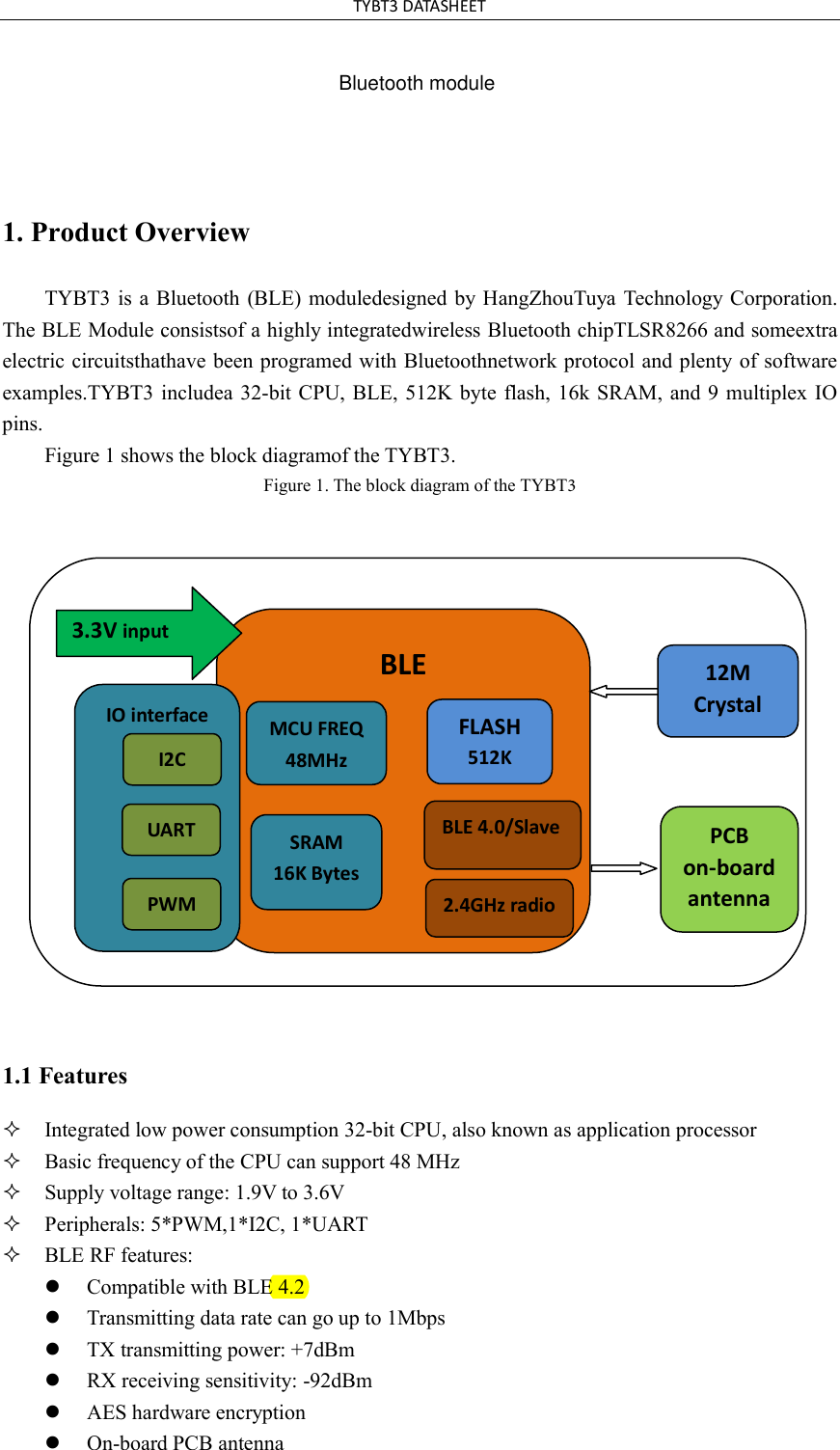
SUNGALE ELECTRONICS TYBT3 Bluetooth module User Manual TYBT2 EN V1x
SUNGALE ELECTRONICS (SHENZHEN) CO., LTD. Bluetooth module TYBT2 EN V1x
UserManual.wiki
>
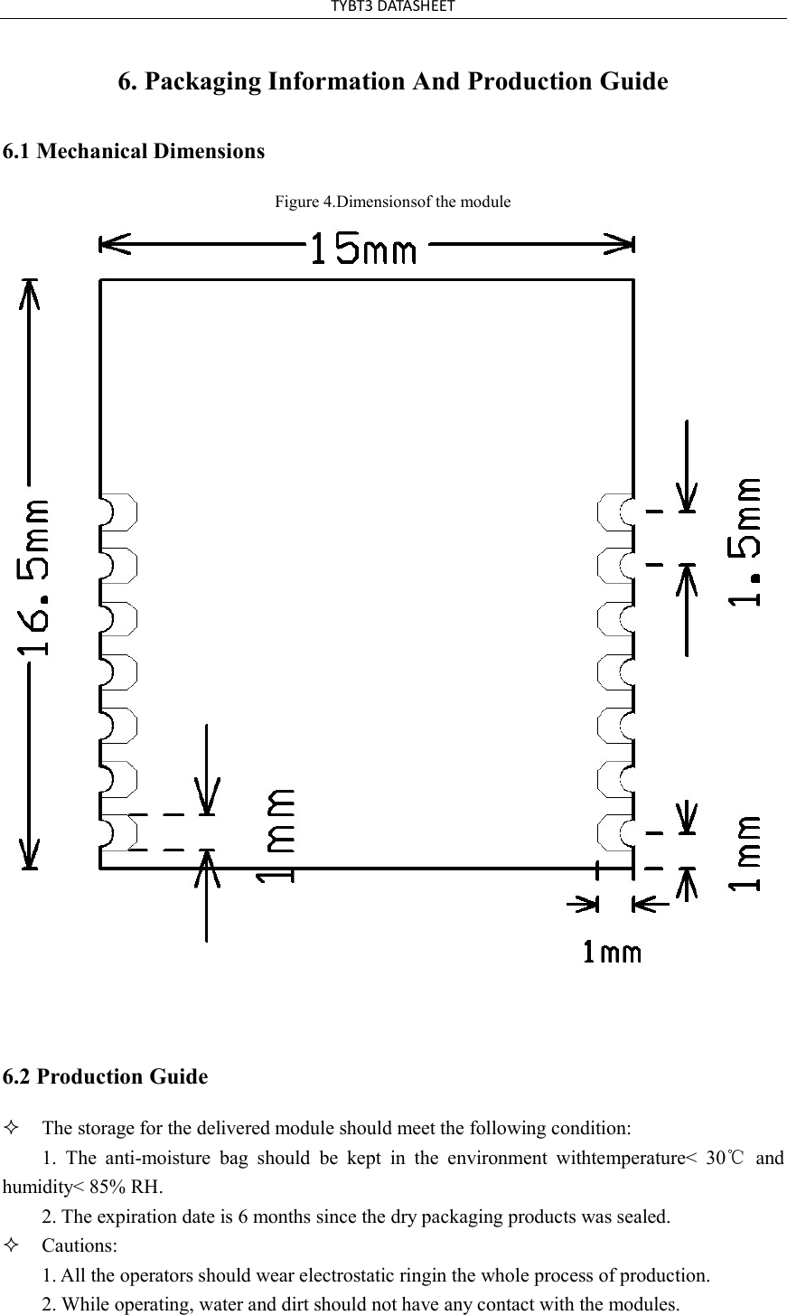
SUNGALE ELECTRONICS
>
TYBT3 User Manual
15_TYBT3 UserMan
Navigation menu
Upload a User Manual
Namespaces
Wiki Guide
HTML
PDF
Info
Views
User Manual
Discussion / Help
Navigation