SUNGALE ELECTRONICS TYBT3 Bluetooth module User Manual TYBT2 EN V1x
SUNGALE ELECTRONICS (SHENZHEN) CO., LTD. Bluetooth module TYBT2 EN V1x
15_TYBT3 UserMan
examples.TYBT3
TYBT3 DATASHEET
1. Product Overview
TYBT3 is a Bluetooth (BLE) moduledesigned by HangZhouTuya Technology Corporation.
The BLE Module consistsof a highly integratedwireless Bluetooth chipTLSR8266 and someextra
electric circuitsthathave been programed with Bluetoothnetwork protocol and plenty of software
includea 32-bit CPU, BLE, 512K byte flash, 16k SRAM, and 9 multiplex IO
pins.
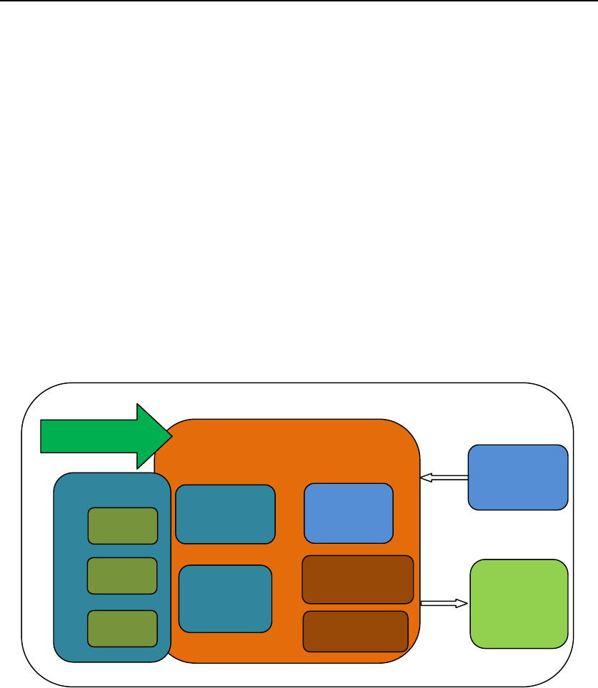
Figure 1 shows the block diagramof the TYBT3.
Figure 1. The block diagram of the TYBT3
1.1 Features
Integrated low power consumption 32-bit CPU, also known as application processor
Basic frequency of the CPU can support 48 MHz
Supply voltage range: 1.9V to 3.6V
Peripherals: 5*PWM,1*I2C, 1*UART
BLE RF features:
Compatible with BLE 4.2
Transmitting data rate can go up to 1Mbps
TX transmitting power: +7dBm
RX receiving sensitivity: -92dBm
AES hardware encryption
On-board PCB antenna
BLE
IO interface
12M
Crystal
PCB
on-board
antenna
BLE 4.0/Slave
2.4GHz radio
MCU FREQ
48MHz
SRAM
16K Bytes
FLASH
512K
I2C
3.3V input
PWM
UART
Bluetooth module

TYBT3 DATASHEET
Operating temperature range: -20℃ to 125℃
1.2 Main ApplicationFields
Intelligent LED
Intelligent household applications
Intelligent low-power consumptionsensors
TYBT3 DATASHEET
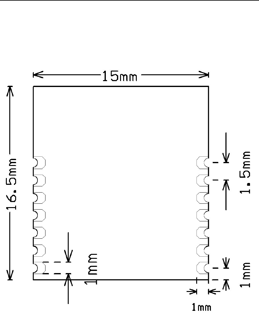
2. Dimensions and Footprint
2.1Dimensions
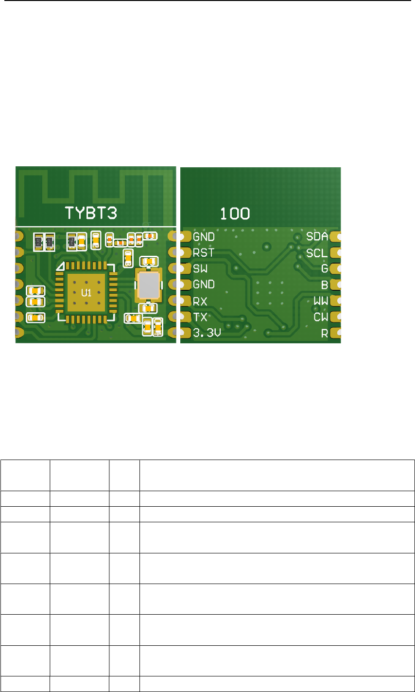
TYBT3have double sides of pins. The distance between each Pin is 2.0mm.
Size of TYBT3: 15mm(W)*16.5mm(L).
Figure 2 shows the dimensions of TYBT3.
Figure 2. The dimensions of TYBT3
2.2 Pin Definition
Table 1 shows the generalpin attributes of TYBT3
Table 1. The typical pin definitionof TYBT3
PIN NO. NAME TYP
E
DESCRIPTION
1 SDA I/O I2C, data interface,internal pull-up 4.7k resistance
2 SCL I/O I2C, clock interface, internal pull-up 4.7k resistance
3 G I/O normal IO pin, can be used as PWM output pin, default for
Green LED line
4 B I/O normal IO pin, can be used as PWM output pin, default for Blue
LED line
5 WW I/O normal IO pin, can be used as PWM output pin, default for
Warm White LED line
6 CW I/O normal IO pin, can be used as PWM output pin, default for Cold
White LED line
7 R I/O normal IO pin, can be used as PWM output pin, default for Red
LED line
8 3.3V P Supply voltage

TYBT3 DATASHEET
9 TX I/O UART TX,can be used as normal IO pin
10 RX I/O UART RX,can be used as normal IO pin
11 GND P Ground
12 SW I/O Bluetooth chipset burning pin
13 RST I reset pin for the module,internal pull-up 4.7k resistance
14 GND P Ground
Note: P: Power supply pins; I/O: Digital input or output pins.
SW pin is ONLY used for burning firmware, Can NOT be used for other functions.
There are 4.7 pull-up resistance internally for I2C pins, external pull-up resistances are not
necessary.
When WW pin is outputting PWM signal, It has opposite phase comparing the PWM signal
from R/G/B/CW pin.
If there’s any customization needed for PWM output, please contact our BD manager.
TYBT3 DATASHEET
3. Electrical Characteristics
3.1 Absolute Maximum Ratings
Table 2. Absolute Maximum Ratings
PARAMETERS DESCRIPTION MIN MAX UNIT
Ts Storage
temperature
-20 125 ℃
VCC Supply voltage -0.3 3.9 V
Electrostatic release quantity
(Human body model)
TAMB-25℃ - 2 KV
Electrostatic release quantity
(Machine model)
TAMB-25℃ - 0.5 KV
3.2 Electrical Conditions
Table 3. Electrical Conditions
PARAMETERS DESCRIPTION MIN TYPIC
AL
MAX UNIT
Ta Temperature for Commercial grade -20 - 125 ℃
VCC Supply voltage
VIL IO negative level input
VIH IO positive level input
VOL IO negative level output
VoH IO positive level output
3.3Transmitting Current Consumptions
Table 4. TX current consumption
PARAMETERS MODE TYPICAL UNIT
Itx Continuously transmitting, 0dBm power output
Irx Continuously receiving
IDC Normal working mode
1.9 3.3 3.6 V
-0.3 - VCC*0.3 V
VCC*0.7 - VCC V
VSS - 0.3 V
VCC-0.3 - VCC V
15 mA
12 mA
27 mA
18 uA
Ideepsleep
Sleep mode
Sleep mode
TYBT3 DATASHEET
4. Radio Specification
4.1 Basic Radio Frequency Characteristics
Table 5.Basic Radio frequency characteristics
PARAMETERS DESCRIPTION
Working Frequency 2.4GHz ISM band
Radio standard BLE 4.2
Data transmitting rate
Type of Antenna On-board PCB Antenna
4.2TransmittingPower
Table 6. Transmitting power
PARAMETERS MIN TYPICAL MAX UNIT
RF Average output power
consumption
3.8 7 dBm
20dB bandwidth - 1300 - KHz
4.3Receiving Sensitivity
Table 7. Receiving sensitivity
PARAMETERS MIN TYPICAL MAX UNIT
RX sensitivity
Frequency bias error
Co-channel interference Restrain - - -7 - dB
1Mbps,2Mbps
8
(1M)
20dB bandwidth (2M) - 2600 - KHz
1Mbps -93 -92 -90
dBm
2Mbps -90 -89 -86
1Mbps -300 - +300
KHz
2Mbps -200 - +200
weld TYBT3 module and other electrical
5.
Antenna Information
5.1 Antenna Type
Antenna for TYBT3
module is
5.2 Reduce Antenna I
nterference
I
n order to have the best
distance
between the antenna part and the other metal pieces.
Since PCB
A manufacture use
components onto the PCB board, RF performance will depend on the layout location and patt
of the On-
board PCB antenna. The following figures are some recommended and
dis-recommended
demonstrations from out R&D team.
In demonstration
1 and 2 of figure 3, the on
frame.
It’s recommended to use layout pattern shown in
on-board PCB antenna lays
outside of the PCB frame directly or PCB frame
area for the antenna. The
overall PCBA
testing the module independently.
Restricted due to some reason, i
frame, it’s suggested to ref
er to demonstration 3.
copperor wire beneath
the antenna.
It’s NOT recommended to use demonstra
there are copper and wire beneath it. RF performance will have
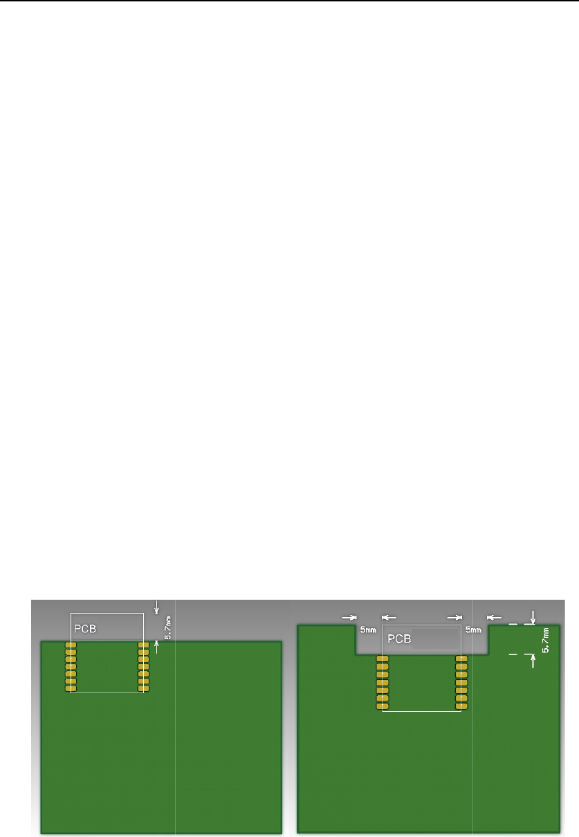
Demonstration 1: Antenna lay outside the
PCB frame
TYBT3 DATASHEET
Antenna Information
module is
using 2.4 GHz MIFAOn-board PCBantenna.
nterference
n order to have the best
RF performance, it’s recommended
to keep a
between the antenna part and the other metal pieces.
A manufacture use
SMT process to
weld TYBT3 module and other electrical
components onto the PCB board, RF performance will depend on the layout location and patt
board PCB antenna. The following figures are some recommended and
demonstrations from out R&D team.
1 and 2 of figure 3, the on
-board PCB antenna lays
outside
It’s recommended to use layout pattern shown in
demonstration
1 and 2. Either the
outside of the PCB frame directly or PCB frame
car
overall PCBA
performance
for these two ways will be the same as
testing the module independently.
Restricted due to some reason, i
f the on-board PCB antenna layo
ut has to be inside the PCB
er to demonstration 3.
The ant
enna lays inside the PCB frame,
the antenna.
RF performance will have some loss, approximately 1~2 dBm.
It’s NOT recommended to use demonstra
tion 4, the antenna
lays inside the PCB frame, and
there are copper and wire beneath it. RF performance will have
significant
attenuation
Figure 3.layoutdemostrations
Demonstration 1: Antenna lay outside the
PCB frame
Demonstration 2: Antenna lay
the PCB frame with carved area
to keep a
minimum15mm
components onto the PCB board, RF performance will depend on the layout location and patt
ern
board PCB antenna. The following figures are some recommended and
outside
of the PCB
1 and 2. Either the
car
ve out a certain
for these two ways will be the same as
ut has to be inside the PCB
enna lays inside the PCB frame,
but no
RF performance will have some loss, approximately 1~2 dBm.
lays inside the PCB frame, and
attenuation
.
Demonstration 2: Antenna lay
outside
the PCB frame with carved area
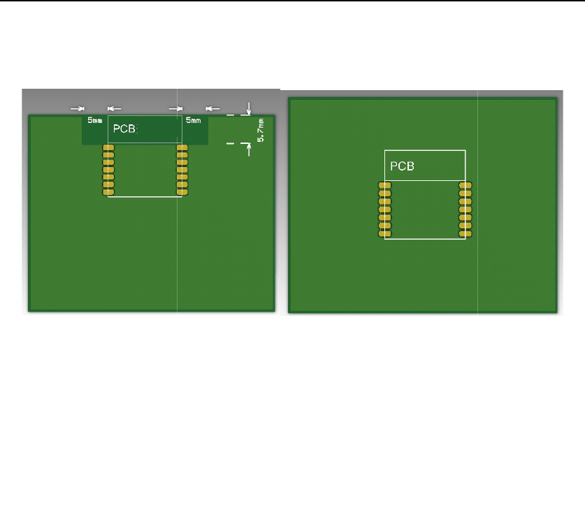
Demonstration 3: Antenna lay inside the PCB
frame
without copper or wire beneath it
TYBT3 DATASHEET
Demonstration 3: Antenna lay inside the PCB
without copper or wire beneath it
Demonstration 4: Antenna lay inside the PCB
frame with copper or wire beneath it
Demonstration 4: Antenna lay inside the PCB
frame with copper or wire beneath it
TYBT3 DATASHEET
6. Packaging Information And Production Guide
6.1 Mechanical Dimensions
Figure 4.Dimensionsof the module
6.2 Production Guide
The storage for the delivered module should meet the following condition:
1. The anti-moisture bag should be kept in the environment withtemperature< 30℃ and
humidity< 85% RH.
2. The expiration date is 6 months since the dry packaging products was sealed.
Cautions:
1. All the operators should wear electrostatic ringin the whole process of production.
2. While operating, water and dirt should not have any contact with the modules.

TYBT3 DATASHEET
This device complies with Part 15 of the FCC rules. Operation is subject to the
following two conditions: 1) this device may not cause harmful interference, and 2)
this device must accept any interference received, including interference that may
cause undesired operation.
Note: This equipment has been tested and found to comply with the limits for a Class
B digital device, pursuant to part 15 of the FCC Rules. These limits are designed to
provide reasonable protection against harmful interference in a residential installation.
This equipment generates uses and can radiate radio frequency energy and, if not
installed and used in accordance with the instructions, may cause harmful
interference to radio communications. However, there is no guarantee that
interference will not occur in particular installation. If this equipment does cause
harmful interference to radio or television reception, which can be determined by
turning the equipment off and on, the user is encouraged to try to correct the
interference by one or more of the following measures:
--Reorient or relocate the receiving antenna.
--Increase the separation between the equipment and receiver.
--Connect the equipment into an outlet on a circuit different from that to which the
receiver is connected.
--Consult the dealer or an experienced radio/TV technician for help.
Changes or modifications not expressly approved by the party responsible for
compliance could void the user’s authority to operate the equipment.
FCC Radiation Exposure Statement
This modular complies with FCC RF radiation exposure limits set forth for an
uncontrolled environment. This transmitter must not be co-located or operating in
conjunction with any other antenna or transmitter.
Note 1: Compliance of this device in all final host configurations is the responsibility of the
Grantee. OEM integrators are responsible to satisfy RF exposure requirements. SAR evaluation is
valid for portable, mobile and fixed applications.
Note 2: Any modifications made to the module will void the Grant of Certification, this module is
limited to OEM installation only and must not be sold to end-users, end-user has no manual
instructions to remove or install the device, only software or operating procedure shall be placed
in the end-user operating manual of final products.
Note 3: The device must not transmit simultaneously with any other antenna or transmitter.
Note 4: To ensure compliance with all non-transmitter functions the host manufacturer is
responsible for ensuring compliance with the module(s) installed and fully operational. For
example, if a host was previously authorized as an unintentional radiator under the Declaration
of Conformity procedure without a transmitter certified module and a module is added, the host
manufacturer is responsible for ensuring that the after the module is installed and operational
the host continues to be compliant with the Part 15B unintentional radiator requirements. Since
this may depend on the details of how the module is integrated with the host, The manufacturer
shall provide guidance to the host manufacturer for compliance with the Part 15B requirements.
Note 5: FCC ID label on the final system must be labeled with “Contains FCC ID: XBI-TYBT3”
The transmitter module must be installed and used in strict accordance with the manufacturer's
instructions as described in the user documentation that comes with the host product.
SUNGALE ELECTRONICS (SHENZHEN) CO.,LTD is responsible for the compliance of the
module in all final hosts.