Samsung Electronics Co ATKM005000 IOT Module User Manual ARTIK 050 Datasheet
Samsung Electronics Co Ltd IOT Module ARTIK 050 Datasheet
UserManual.wiki
>
Samsung Electronics Co
>
ATKM005000 User Manual
User Manual
Navigation menu
Upload a User Manual
Namespaces
Wiki Guide
HTML
PDF
Info
Views
User Manual
Discussion / Help
Navigation
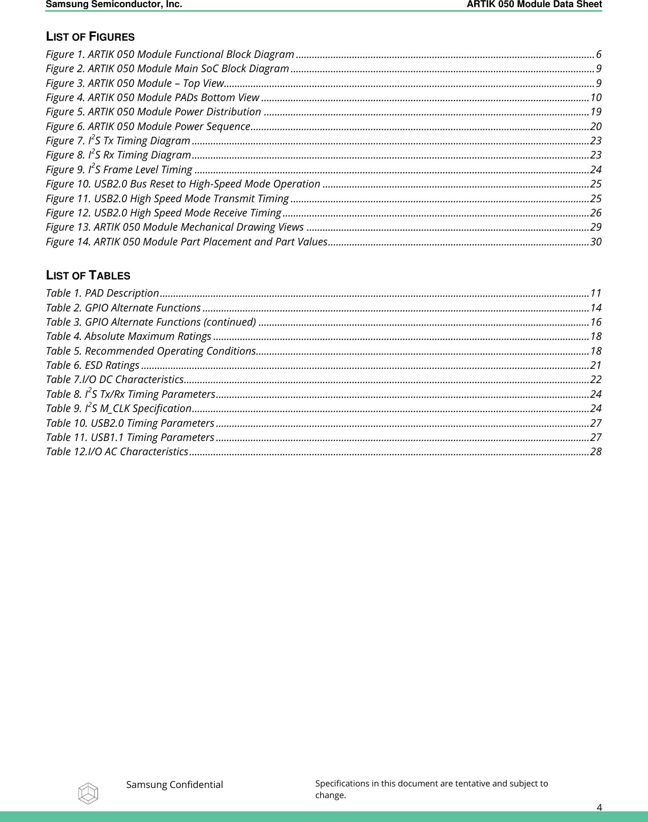
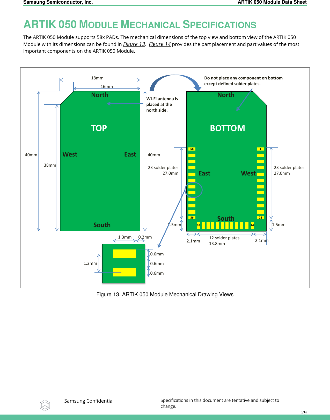
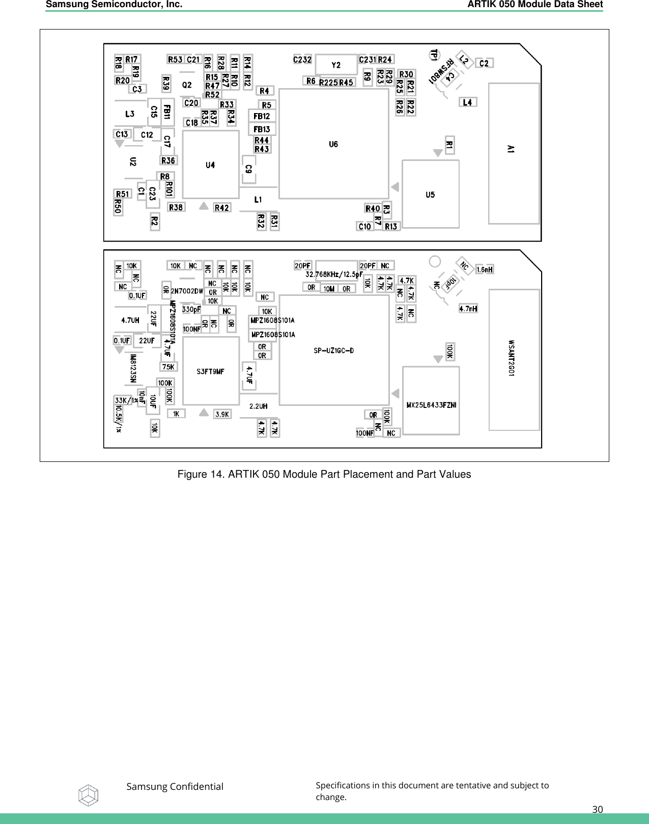
![Samsung Semiconductor, Inc. ARTIK 050 Module Data Sheet Samsung Confidential Specifications in this document are tentative and subject to change. 11 Table 1. PAD Description PAD# Name Voltage [V] I/O Type DF Active Mode Low Power Mode Power Down Mode DS [mA] Default Function Comments Comments for Design 1 I2C_0_SCL 3V35 BCM I/O PU - - - - - I2C0 CLK Internal 4.7K / 3.3V Pull-up 2 I2C_0_SDA 3V35 BCM I/O PU - - - - - I2C0 DATA Internal 4.7K / 3.3V Pull-up 3 PWM_5 3V35 BCM I/O - - - - - - PWM 5 4 PWM_4 3V35 BCM I/O - - - - - - PWM 4 5 PWM_3 3V35 BCM I/O - - - - - - PWM 3 6 PWM_2 3V35 BCM I/O - - - - - - PWM 2 7 PWM_0 3V35 BCM I/O - - - - - - PWM 0 8 PWM_1 3V35 BCM I/O - - - - - - PWM 1 9 GPIO_0 3V35 BCM I/O IN/PD IO/PU/PD/NP IO/PU/PD/NP High-Z/NP 8 USB20H_CTL GPIO 0 For USB mode, need to connect overcurrent flag pin with 4.7K Pull-up 10 GND 0V0 NA NA NA NA NA NA NA Ground 11 USB2_DN 3V35 BCM USB - - - - - - USB2_DN 12 USB2_DP 3V35 BCM USB - - - - - - USB2_DP 13 GND 0V0 NA NA NA NA NA NA NA Ground 14 GPIO_7_WCPU_BOOT_MODE 3V35 BCM I/O IN/PU IO/PU/PD/NP IO/PU/PD/NP High-Z/NP 8 - Boot Wireless CPU from Tightly Coupled RAM Internal 10K/3.3V Pull-up for boot mode : not recommended Pull down resistor 15 GPIO_8_TAP_SEL 3V35 BCM I/O IN/PU IO/PU/PD/NP IO/PU/PD/NP High-Z/NP 8 GPIO_8 GPIO 8, default function TAP_SEL_P Internal 10K/3.3V Pull-up for boot mode : not recommended Pull-down resistor Only fo Input, Not support Output 16 GPIO_9_USB_HSIC_SEL 3V35 BCM I IN/PU IO/PU/PD/NP IO/PU/PD/NP High-Z/NP 8 GPIO_9 USB 2.0 PHY is selected Internal 10K/3.3V Pull-up for boot mode : not recommended Pull-down resistor 17 GPIO_11_ACPU_BOOT_MODE 3V35 BCM I/O IN/PD IO/PU/PD/NP IO/PU/PD/NP High-Z/NP 8 - Boot Main CPU from internal ROM For boot mode : not recommended Pull-up resistor 18 UART_TXD 3V35 BCM UART (LS) - - - - - - Level Shifted UART_TXD Level Shifted UART_TXD, need to Pull-up resistor for UART communication](https://usermanual.wiki/Samsung-Electronics-Co/ATKM005000/User-Guide-3081745-Page-11.png)
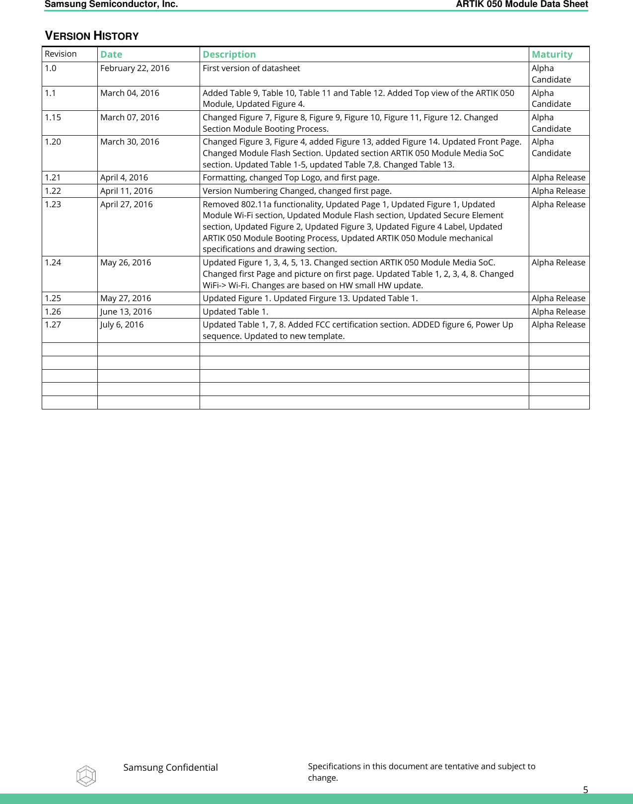
![Samsung Semiconductor, Inc. ARTIK 050 Module Data Sheet Samsung Confidential Specifications in this document are tentative and subject to change. 12 PAD# Name Voltage [V] I/O Type DF Active Mode Low Power Mode Power Down Mode DS [mA] Default Function Comments Comments for Design 19 UART_RXD 3V35 BCM UART (LS) - - - - - - Level Shifted UART_RXD Level Shifted UART_RXD, need to Pull-up resistor for UART communication 1K serial resistor after Level-shifter, not recommended serial resister over 1K 20 GND 0V0 NA NA NA NA NA NA NA Ground 21 GPIO_12 3V35 BCM I/O IN/NP IO/PU/PD/NP IO/PU/PD/NP High-Z/NP 8 GPIO_12 GPIO 12 22 GPIO_14 3V35 BCM I/O IN/NP IO/PU/PD/NP IO/PU/PD/NP High-Z/NP 8 GPIO_14 GPIO 14 23 GPIO_13_SDIO_MODE 3V35 BCM I/O IN/PU IO/PU/PD/NP IO/PU/PD/NP High-Z/NP 8 - GPIO 13 boot strap SDIO_MODE Internal 10K/3.3V Pull-up for boot mode : not recommended Pull up resistor 24 GPIO_15_HOST_VTRIM 3V35 BCM I/O IN/PD IO/PU/PD/NP IO/PU/PD/NP High-Z/NP 8 - GPIO 15 boot strap VTRIM_EN for boot mode : not recommanded Pull-up resistor 25 GPIO_16 3V35 BCM I/O IN/NP IO/PU/PD/NP IO/PU/PD/NP High-Z/NP 8 - GPIO 16 26 I2S0_MCK 3V35 BCM I/O - - - - - - I2S 0 MCK 27 I2S0_SCK_BLCK 3V35 BCM I/O - - - - - - I2S 0 SCK_BLCK 28 I2S0_SD_OUT 3V35 BCM I/O - - - - - - I2S 0 SD_OUT 29 I2S0_WS_LRCLK 3V35 BCM I/O - - - - - - I2S 0 WS_LRCLK 30 PWR_RST NA Power En Input - - - - - - if PWR_RST is 0 DCDC disabled 150Kohm PU, 75Kohm PD, VIH 1.45V, VIL 0.4V 31 GND 0V0 NA NA NA NA NA NA NA Ground Ground 32 VIN 4V5 Power Input NA NA NA NA NA NA Power MIN 4.75 ~ MAX 18V 33 SPI_0_CLK 3V35 BCM I/O - - - - - - SPI 0 CLK 34 SPI_0_MOSI 3V35 BCM I/O - - - - - - SPI 0 MOSI 35 SPI_0_MISO 3V35 BCM I/O - - - - - - SPI 0 MISO 36 SPI_0_CS 3V35 BCM I/O - - - - - - SPI 0 CS 37 3.3V_OUT 3V35 NA NA NA NA NA NA NA Power Power pin for 050 IO port, Current limit 100mA @3.3V 38 RESET_N 3V35 BCM RESET - - - - - - Reset ARTIK 050 Module Reset pin, not recommended Pull-down resister 39 GPIO_3_JTAG_TMS 3V35 BCM I/O IN/PD IO/PU/PD/NP IO/PU/PD/NP High-Z/NP 8 GCI_GPIO(1) Debug_JTAG 40 GPIO_4_JTAG_TDI 3V35 BCM I/O IN/NP IO/PU/PD/NP IO/PU/PD/NP High-Z/NP 8 GCI_GPIO(2) Debug_JTAG](https://usermanual.wiki/Samsung-Electronics-Co/ATKM005000/User-Guide-3081745-Page-12.png)
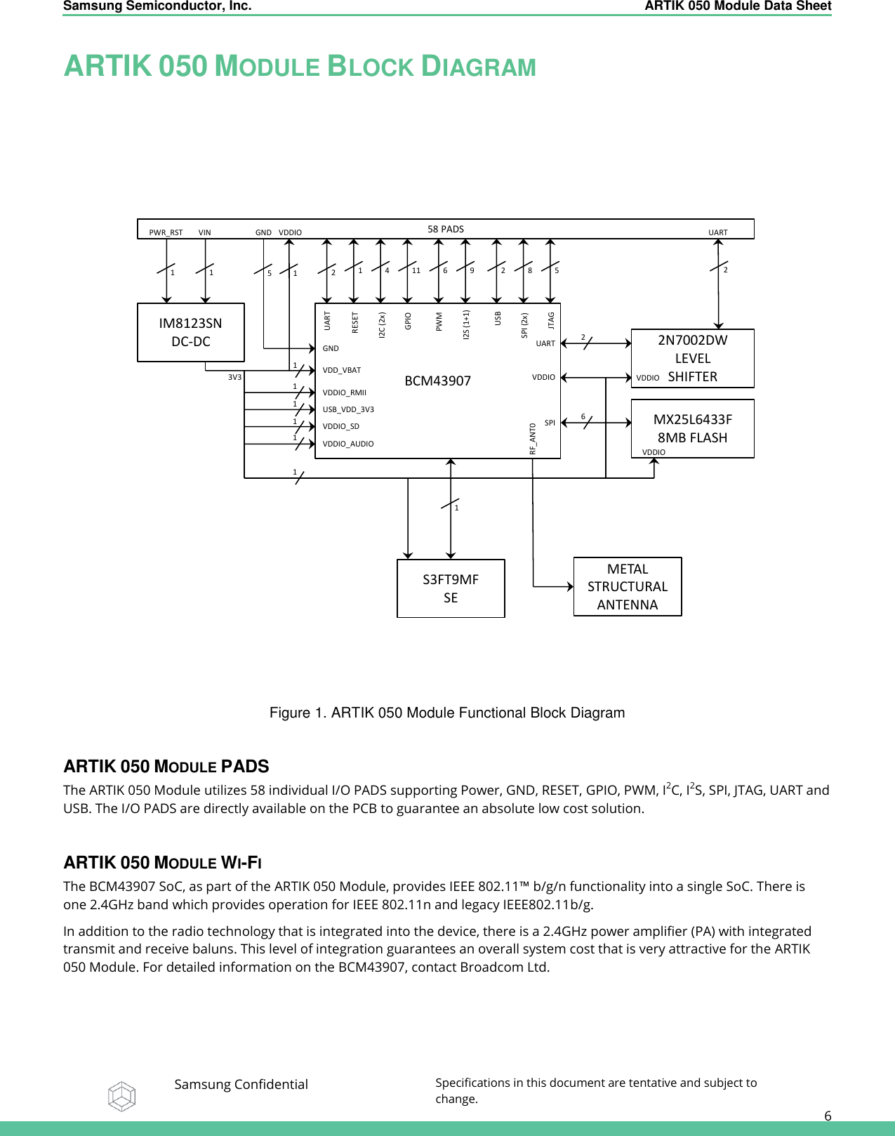
![Samsung Semiconductor, Inc. ARTIK 050 Module Data Sheet Samsung Confidential Specifications in this document are tentative and subject to change. 13 PAD# Name Voltage [V] I/O Type DF Active Mode Low Power Mode Power Down Mode DS [mA] Default Function Comments Comments for Design 41 GPIO_2_JTAG_TCK 3V35 BCM I/O NP IO/PU/PD/NP IO/PU/PD/NP High-Z/NP 8 GCI_GPIO(0) Debug_JTAG 42 GPIO_5_JTAG_TDO 3V35 BCM I/O IN/PD IO/PU/PD/NP IO/PU/PD/NP High-Z/NP 8 GCI_GPIO(3) Debug_JTAG 43 GPIO_6_JTAG_TRST_L 3V35 BCM I/O IN/NP IO/PU/PD/NP IO/PU/PD/NP High-Z/NP 8 GCI_GPIO(4) Debug_JTAG 44 GND 0V0 NA NA NA NA NA NA NA Ground 45 RF_SW_CTRL_6_UART1_RX_IN 3V35 BCM I/O OUT/NP O/NP O/NP High-Z - - RF_SW+CTRL_6 Debug_UART_RX 46 RF_SW_CTRL_7_RSRC_INIT_MODE_UART1_TX_OUT 3V35 BCM I/O IN/PD O/NP O/NP High-Z - - RF_SW+CTRL_7 PMU enable strap Debug_UART_TX 47 I2C_1_SCL 3V35 BCM I/O PU - - - - - I2C 1 SCL Internal 4.7K/3.3V Pull-up 48 I2C_1_SDA 3V35 BCM I/O PU - - - - - I2C 1 SDA Internal 4.7K/3.3V Pull-up 49 I2S1_WS_LRCLK 3V35 BCM I/O - - - - - - I2S 1 WS_LRCLK 50 I2S1_SD_OUT 3V35 BCM I/O - - - - - - I2S 1 SD_OUT 51 I2S1_SD_IN 3V35 BCM I/O - - - - - - I2S 1 SD_IN 52 I2S1_SCK_BCLK 3V35 BCM I/O - - - - - - I2S 1 SCK_BCLK 53 I2S1_MCK 3V35 BCM I/O - - - - - - I2S 1 MCK 54 SPI_1_MOSI 3V35 BCM I/O - - - - - - SPI 1 MOSI 55 SPI_1_CS 3V35 BCM I/O - - - - - - SPI 1 CS 56 SPI_1_MISO 3V35 BCM I/O - - - - - - SPI 1 MISO 57 SPI_1_CLK 3V35 BCM I/O - - - - - - SPI 1 CLK 58 GPIO_1_GSPI_MODE 3V35 BCM I/O NP IO/PU/PD/NP IO/PU/PD/NP High-Z/NP 8 - GPIO 1 with GSPI_MODE strap For boot mode : not recommended Pull-up resistor *PU = Pull Up, PD = Pull Down, NP = No Pull](https://usermanual.wiki/Samsung-Electronics-Co/ATKM005000/User-Guide-3081745-Page-13.png)
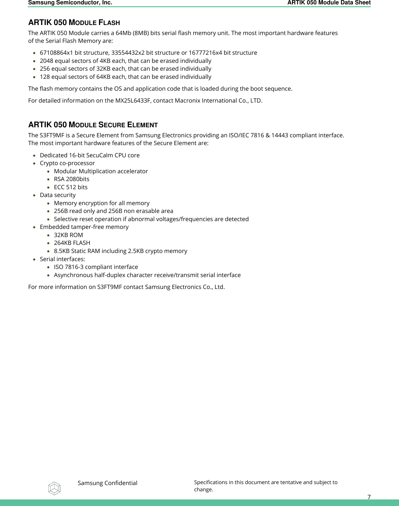
![Samsung Semiconductor, Inc. ARTIK 050 Module Data Sheet Samsung Confidential Specifications in this document are tentative and subject to change. 18 ARTIK 050 MODULE ELECTRICAL SPECIFICATIONS ABSOLUTE MAXIMUM RATINGS Absolute maximum ratings are those ratings where permanent damage to the ARTIK 050 Module can occur. Functional operation at absolute maximum ratings is not guaranteed and not recommended. Table 4. Absolute Maximum Ratings PAD:[Pin#] Symbol Condition Min Typ Max Units PAD:[32] VIN Input voltage VIN on the high efficiency step down converter (IM8123SM) – – 20 V PAD:[1,2,3,4,5,6,7,8,9,14,15, 16,17,21,22,23,24,25,26,27, 28,29,33,34,35,36,39,40, 41,42,43,45,46,47,48,49,50, 51,52,53,54,55,56,57,58] Vundershoot Undershoot voltage for I/O -0.50 – – V PAD:[30] PWR_RST – -0.30 – 20.3 V PAD:[18,19] VMAX IO is running at 3.3V level shifter is closed so 60+3.3 – – 63.3 V IMAX Continuous – – 115 mA Continuous at 100°C – – 73 mA Pulsed – – 800 mA RECOMMENDED OPERATING CONDITIONS The following table describes the operating conditions of the ARTIK 050 Module: Table 5. Recommended Operating Conditions PAD:[Pin#] Symbol Condition Min Typ Max Units PAD:[32] VIN Input voltage VIN on the high efficiency step down converter (IM8123SM) 4.50 – 18.0 V – TO Maximum operating temperature -25 – 85 °C TS Storage temperature -40 – 125 °C](https://usermanual.wiki/Samsung-Electronics-Co/ATKM005000/User-Guide-3081745-Page-18.png)
![Samsung Semiconductor, Inc. ARTIK 050 Module Data Sheet Samsung Confidential Specifications in this document are tentative and subject to change. 22 DC ELECTRICAL CHARACTERISTICS Table 7 below describes the DC characteristics for all GPIO pins that are available on the PAD. Table 7.I/O DC Characteristics PAD:[Pin#] Symbol Condition Min Typ Max Units PAD:[1,2,3,4,5,6,7,8,9,14, 15,16,17,21,22,23,24,25, 26,27,28,29,33,34,35, 36,39,40,41,42,43,45,46, 47,48,49,50,51,52,53,54, 55,56,57,58] VIH Input high voltage 2.00 – – V VIL Input low voltage – – 0.80 V VOH Output high voltage @ 2mA 2.90 – – V VOL Output low voltage @ 2mA – – 0.40 V PAD:[19] VIH Input high voltage 3.5 5 20 V VIL Input low voltage – – 0.2 V PAD:[45,46]* CIN Input capacitance – – 5 pF *Programmable 2mA to 16mA drive strength. The default is 10mA.](https://usermanual.wiki/Samsung-Electronics-Co/ATKM005000/User-Guide-3081745-Page-22.png)
![Samsung Semiconductor, Inc. ARTIK 050 Module Data Sheet Samsung Confidential Specifications in this document are tentative and subject to change. 28 Table 12.I/O AC Characteristics PAD:[Pin#] Symbol Condition Min Typ Max Units PAD:[18,19] Dynamic Characteristics CISS Input Capacitance VPAD:[33,34,35,36]=28.3V, f=1.0MHz – 37.8 50 pF COSS Output Capacitance – 12.4 25 pF CRSS Reverse Transfer Capacitance – 6.5 7 pF Switching Characteristics tD(ON) Turn-on Delay Time V*PAD-PAD =30V, IPAD-PAD=0.2A, VGEN=10V, RL=150Ω, RGEN=25Ω – 5.85 20 ns tD(OFF) Turn-off Delay Time – 12.5 20 ns *PAD-PAD means from PAD:[18] to PAD:[18] or from PAD:[19] to PAD:[19], it is the voltage swing over time on PAD:[18] or PAD:[19]](https://usermanual.wiki/Samsung-Electronics-Co/ATKM005000/User-Guide-3081745-Page-28.png)