Samsung Electronics Co ATKM005000 IOT Module User Manual ARTIK 050 Datasheet
Samsung Electronics Co Ltd IOT Module ARTIK 050 Datasheet
User Manual
Samsung Semiconductor, Inc. ARTIK 050 Module Data Sheet
Samsung Confidential
Specifications in this document are tentative and subject to
change.
2
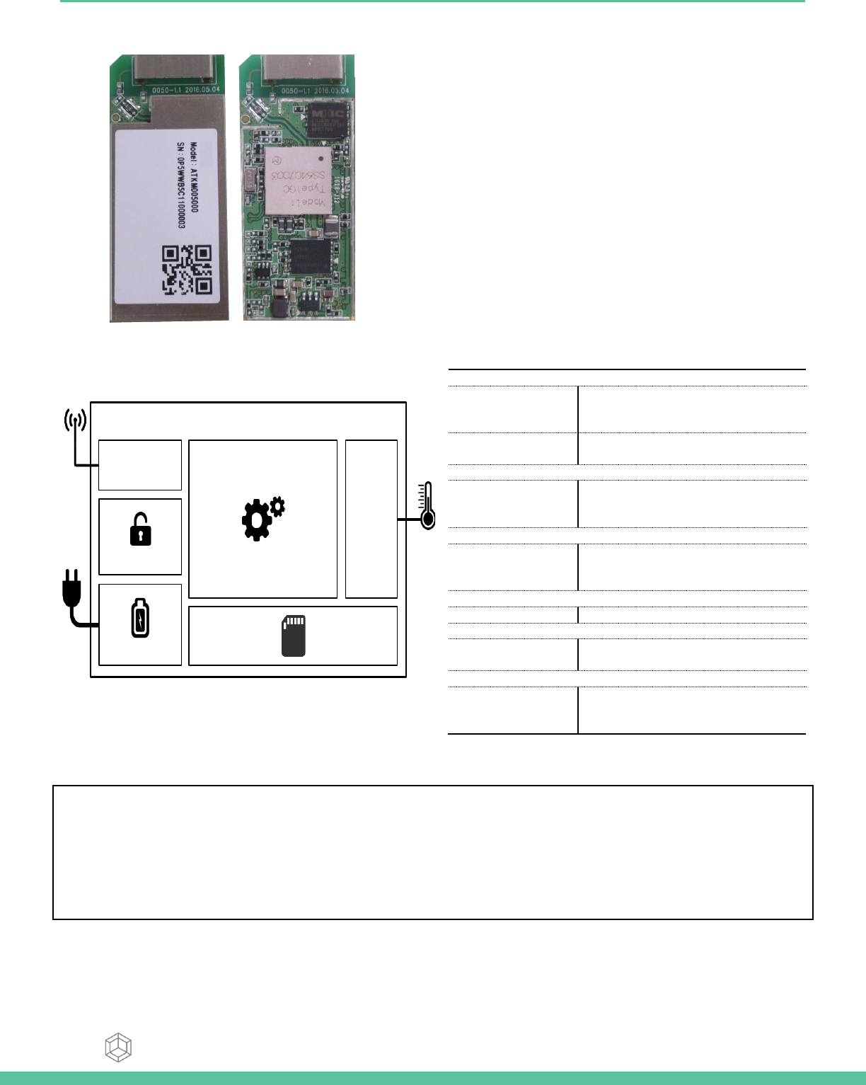
Top View
Samsung’s ARTIK™ 050 Module is a highly-integrated
module for secure Internet of Things (IoT) devices that
require Wi-Fi. It is based on an ARM® Cortex® -R4 core with
on-chip memories, a complete 2.4GHz Wi-Fi Phy, MAC layer
processing, a large complement of standard digital buses,
including audio (I2S), and power management. The module
is packaged with additional external Flash memory, a
hardware Secure Element and a single integrated 2.4GHz
structural antenna.
The application processor is fully available for applications,
since the Wi-Fi stack through the MAC layer is handled by a
co-processor. Aimed especially at power-sensitive devices
needing Wi-Fi, the ARTIK 050 Module provides excellent
performance in a portable environment, with a feature set
tailored specifically for IoT end nodes.
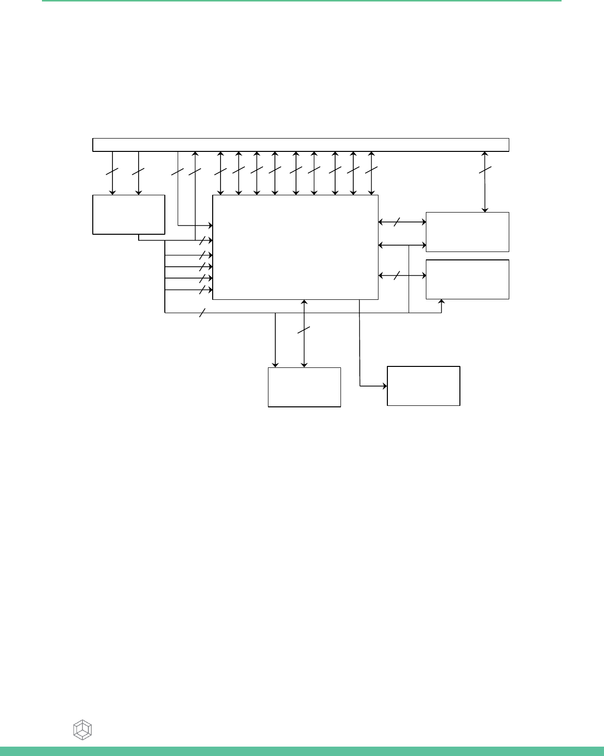
ARTIK 050 Module Block Diagram
Processor
Main CPU
ARM Cortex-R4, 32-bit address and
data paths @ 320MHz, 32KB I$, 32KB
D$
WLAN CPU
ARM Cortex-R4,32-bit address and data
paths @ 160MHz
Memory
User Embedded
RAM
2MB
FLASH
8MB SPI Flash on Module
Security
Secure Element
Hardware-protected key storage with
secure point-to-point authentication
and data transfer
Radio
Wi-Fi
IEEE802.11™ b/g/n 2.4GHz radio
Power Management
Single Supply
Provides all power on the ARTIK 050
Module using on board regulators
Interfaces
Digital I/O
USB2.0, 2x I2C, 1x I2S, 2x SPI, 2x 2-UART,
6x PWM, 11x GPIOs (Dedicated), 5x
GPIOs (Multiplexed)
SAMSUNG ELECTRONICS RESERVES THE RIGHT TO CHANGE PRODUCTS, INFORMATION AND SPECIFICATIONS WITHOUT NOTICE.
Products and specifications discussed herein are for reference purposes only. All information discussed herein is provided on an "AS IS" basis, without warranties
of any kind. This document and all information discussed herein remain the sole and exclusive property of Samsung Electronics. No license of any patent,
copyright, mask work, trademark or any other intellectual property right is granted by one party to the other party under this document, by implication, estoppel
or other-wise. Samsung products are not intended for use in life support, critical care, medical, safety equipment, or similar applications where product failure
could result in loss of life or personal or physical harm, or any military or defense application, or any governmental procurement to which special terms or
provisions may apply. For updates or additional information about Samsung products, contact your nearest Samsung office. All brand names, trademarks and
registered trademarks belong to their respective owners.
ARTIK 050 MODULE
RADIO
SECURITY
PROCESSOR
POWER MGT. MEMORY
INTERFACES

Samsung Semiconductor, Inc. ARTIK 050 Module Data Sheet
Samsung Confidential
Specifications in this document are tentative and subject to
change.
3
TABLE OF CONTENTS
Table of Contents ................................................................................................................................................................... 3
List of Figures ........................................................................................................................................................................................ 4
List of Tables .......................................................................................................................................................................................... 4
Version History ...................................................................................................................................................................................... 5
ARTIK 050 Module Block Diagram ....................................................................................................................................... 6
ARTIK 050 Module PADS ....................................................................................................................................................................... 6
ARTIK 050 Module Wi-Fi ....................................................................................................................................................................... 6
ARTIK 050 Module Flash ....................................................................................................................................................................... 7
ARTIK 050 Module Secure Element ..................................................................................................................................................... 7
ARTIK 050 Module Power Management ............................................................................................................................................. 8
ARTIK 050 Module Media SoC.............................................................................................................................................................. 8
ARTIK 050 Module PADs ...................................................................................................................................................... 10
ARTIK 050 Module GPIO Alternate Functions ................................................................................................................... 14
ARTIK 050 Module Booting Process ................................................................................................................................... 17
ARTIK 050 Module Electrical Specifications ...................................................................................................................... 18
Absolute Maximum Ratings ............................................................................................................................................................... 18
Recommended Operating Conditions .............................................................................................................................................. 18
Power Supply Requirements .............................................................................................................................................................. 19
ESD Ratings .......................................................................................................................................................................................... 21
DC Electrical Characteristics .............................................................................................................................................................. 22
AC Electrical Characteristics .............................................................................................................................................................. 23
ARTIK 050 Module Mechanical Specifications .................................................................................................................. 29
Ordering Information .......................................................................................................................................................... 31
FCC Certification ................................................................................................................................................................... 32
Legal Information ................................................................................................................................................................. 33

Samsung Semiconductor, Inc. ARTIK 050 Module Data Sheet
Samsung Confidential
Specifications in this document are tentative and subject to
change.
4
LIST OF FIGURES
Figure 1. ARTIK 050 Module Functional Block Diagram ................................................................................................................ 6
Figure 2. ARTIK 050 Module Main SoC Block Diagram .................................................................................................................. 9
Figure 3. ARTIK 050 Module – Top View........................................................................................................................................... 9
Figure 4. ARTIK 050 Module PADs Bottom View ........................................................................................................................... 10
Figure 5. ARTIK 050 Module Power Distribution .......................................................................................................................... 19
Figure 6. ARTIK 050 Module Power Sequence ............................................................................................................................... 20
Figure 7. I2S Tx Timing Diagram ..................................................................................................................................................... 23
Figure 8. I2S Rx Timing Diagram ..................................................................................................................................................... 23
Figure 9. I2S Frame Level Timing .................................................................................................................................................... 24
Figure 10. USB2.0 Bus Reset to High-Speed Mode Operation .................................................................................................... 25
Figure 11. USB2.0 High Speed Mode Transmit Timing ................................................................................................................ 25
Figure 12. USB2.0 High Speed Mode Receive Timing ................................................................................................................... 26
Figure 13. ARTIK 050 Module Mechanical Drawing Views .......................................................................................................... 29
Figure 14. ARTIK 050 Module Part Placement and Part Values.................................................................................................. 30
LIST OF TABLES
Table 1. PAD Description ................................................................................................................................................................. 11
Table 2. GPIO Alternate Functions ................................................................................................................................................. 14
Table 3. GPIO Alternate Functions (continued) ............................................................................................................................ 16
Table 4. Absolute Maximum Ratings ............................................................................................................................................. 18
Table 5. Recommended Operating Conditions............................................................................................................................. 18
Table 6. ESD Ratings ........................................................................................................................................................................ 21
Table 7.I/O DC Characteristics ........................................................................................................................................................ 22
Table 8. I2S Tx/Rx Timing Parameters ............................................................................................................................................ 24
Table 9. I2S M_CLK Specification ..................................................................................................................................................... 24
Table 10. USB2.0 Timing Parameters ............................................................................................................................................ 27
Table 11. USB1.1 Timing Parameters ............................................................................................................................................ 27
Table 12.I/O AC Characteristics ...................................................................................................................................................... 28
Samsung Semiconductor, Inc. ARTIK 050 Module Data Sheet
Samsung Confidential
Specifications in this document are tentative and subject to
change.
5
VERSION HISTORY
Revision
Date
Description
Maturity
1.0
February 22, 2016
First version of datasheet
Alpha
Candidate
1.1
March 04, 2016
Added Table 9, Table 10, Table 11 and Table 12. Added Top view of the ARTIK 050
Module, Updated Figure 4.
Alpha
Candidate
1.15
March 07, 2016
Changed Figure 7, Figure 8, Figure 9, Figure 10, Figure 11, Figure 12. Changed
Section Module Booting Process.
Alpha
Candidate
1.20
March 30, 2016
Changed Figure 3, Figure 4, added Figure 13, added Figure 14. Updated Front Page.
Changed Module Flash Section. Updated section ARTIK 050 Module Media SoC
section. Updated Table 1-5, updated Table 7,8. Changed Table 13.
Alpha
Candidate
1.21
April 4, 2016
Formatting, changed Top Logo, and first page.
Alpha Release
1.22
April 11, 2016
Version Numbering Changed, changed first page.
Alpha Release
1.23
April 27, 2016
Removed 802.11a functionality, Updated Page 1, Updated Figure 1, Updated
Module Wi-Fi section, Updated Module Flash section, Updated Secure Element
section, Updated Figure 2, Updated Figure 3, Updated Figure 4 Label, Updated
ARTIK 050 Module Booting Process, Updated ARTIK 050 Module mechanical
specifications and drawing section.
Alpha Release
1.24
May 26, 2016
Updated Figure 1, 3, 4, 5, 13. Changed section ARTIK 050 Module Media SoC.
Changed first Page and picture on first page. Updated Table 1, 2, 3, 4, 8. Changed
WiFi-> Wi-Fi. Changes are based on HW small HW update.
Alpha Release
1.25
May 27, 2016
Updated Figure 1. Updated Firgure 13. Updated Table 1.
Alpha Release
1.26
June 13, 2016
Updated Table 1.
Alpha Release
1.27
July 6, 2016
Updated Table 1, 7, 8. Added FCC certification section. ADDED figure 6, Power Up
sequence. Updated to new template.
Alpha Release
Samsung Semiconductor, Inc. ARTIK 050 Module Data Sheet
Samsung Confidential
Specifications in this document are tentative and subject to
change.
6
ARTIK 050 MODULE BLOCK DIAGRAM
Figure 1. ARTIK 050 Module Functional Block Diagram
ARTIK 050 MODULE PADS
The ARTIK 050 Module utilizes 58 individual I/O PADS supporting Power, GND, RESET, GPIO, PWM, I2C, I2S, SPI, JTAG, UART and
USB. The I/O PADS are directly available on the PCB to guarantee an absolute low cost solution.
ARTIK 050 MODULE WI-FI
The BCM43907 SoC, as part of the ARTIK 050 Module, provides IEEE 802.11™ b/g/n functionality into a single SoC. There is
one 2.4GHz band which provides operation for IEEE 802.11n and legacy IEEE802.11b/g.
In addition to the radio technology that is integrated into the device, there is a 2.4GHz power amplifier (PA) with integrated
transmit and receive baluns. This level of integration guarantees an overall system cost that is very attractive for the ARTIK
050 Module. For detailed information on the BCM43907, contact Broadcom Ltd.
BCM43907
MX25L6433F
8MB FLASH
S3FT9MF
SE
6
58 PADS
SPI
PWM
6
RESET
1
I2C (2x)
4
GPIO
11 2
USB
9
I2S (1+1)
8
SPI (2x)
UART 22N7002DW
LEVEL
SHIFTER
2
5
JTAG
2
UART
5
GND
VDD_VBAT
1
IM8123SN
DC-DC
VIN
VDDIO
1
UART
USB_VDD_3V3
1
VDDIO_RMII
1
VDDIO_AUDIO
1
VDDIO_SD
1
1
1
GND
VDDIO
3V3 VDDIO
1
VDDIO
METAL
STRUCTURAL
ANTENNA
RF_ANT0
1
PWR_RST

Samsung Semiconductor, Inc. ARTIK 050 Module Data Sheet
Samsung Confidential
Specifications in this document are tentative and subject to
change.
7
ARTIK 050 MODULE FLASH
The ARTIK 050 Module carries a 64Mb (8MB) bits serial flash memory unit. The most important hardware features
of the Serial Flash Memory are:
67108864x1 bit structure, 33554432x2 bit structure or 16777216x4 bit structure
2048 equal sectors of 4KB each, that can be erased individually
256 equal sectors of 32KB each, that can be erased individually
128 equal sectors of 64KB each, that can be erased individually
The flash memory contains the OS and application code that is loaded during the boot sequence.
For detailed information on the MX25L6433F, contact Macronix International Co., LTD.
ARTIK 050 MODULE SECURE ELEMENT
The S3FT9MF is a Secure Element from Samsung Electronics providing an ISO/IEC 7816 & 14443 compliant interface.
The most important hardware features of the Secure Element are:
Dedicated 16-bit SecuCalm CPU core
Crypto co-processor
Modular Multiplication accelerator
RSA 2080bits
ECC 512 bits
Data security
Memory encryption for all memory
256B read only and 256B non erasable area
Selective reset operation if abnormal voltages/frequencies are detected
Embedded tamper-free memory
32KB ROM
264KB FLASH
8.5KB Static RAM including 2.5KB crypto memory
Serial interfaces:
ISO 7816-3 compliant interface
Asynchronous half-duplex character receive/transmit serial interface
For more information on S3FT9MF contact Samsung Electronics Co., Ltd.

Samsung Semiconductor, Inc. ARTIK 050 Module Data Sheet
Samsung Confidential
Specifications in this document are tentative and subject to
change.
8
ARTIK 050 MODULE POWER MANAGEMENT
The ARTIK 050 Module has dedicated power management, containing an IM8123SN high-efficiency step-down
DC-DC convertor. The power management is set up such that it provides all power requirements for the module.
The most important features of the power management on the ARTIK 050 Module are:
Wide input range 4.5V ≤ VIN ≤ 18V
Low shut down current Ishutdown ~ 5µA
Thermal shutdown protection
High Switching Frequency 500 kHz
For additional information on the IM8123SN, contact IMS Semiconductor Co., Ltd.
ARTIK 050 MODULE MEDIA SOC
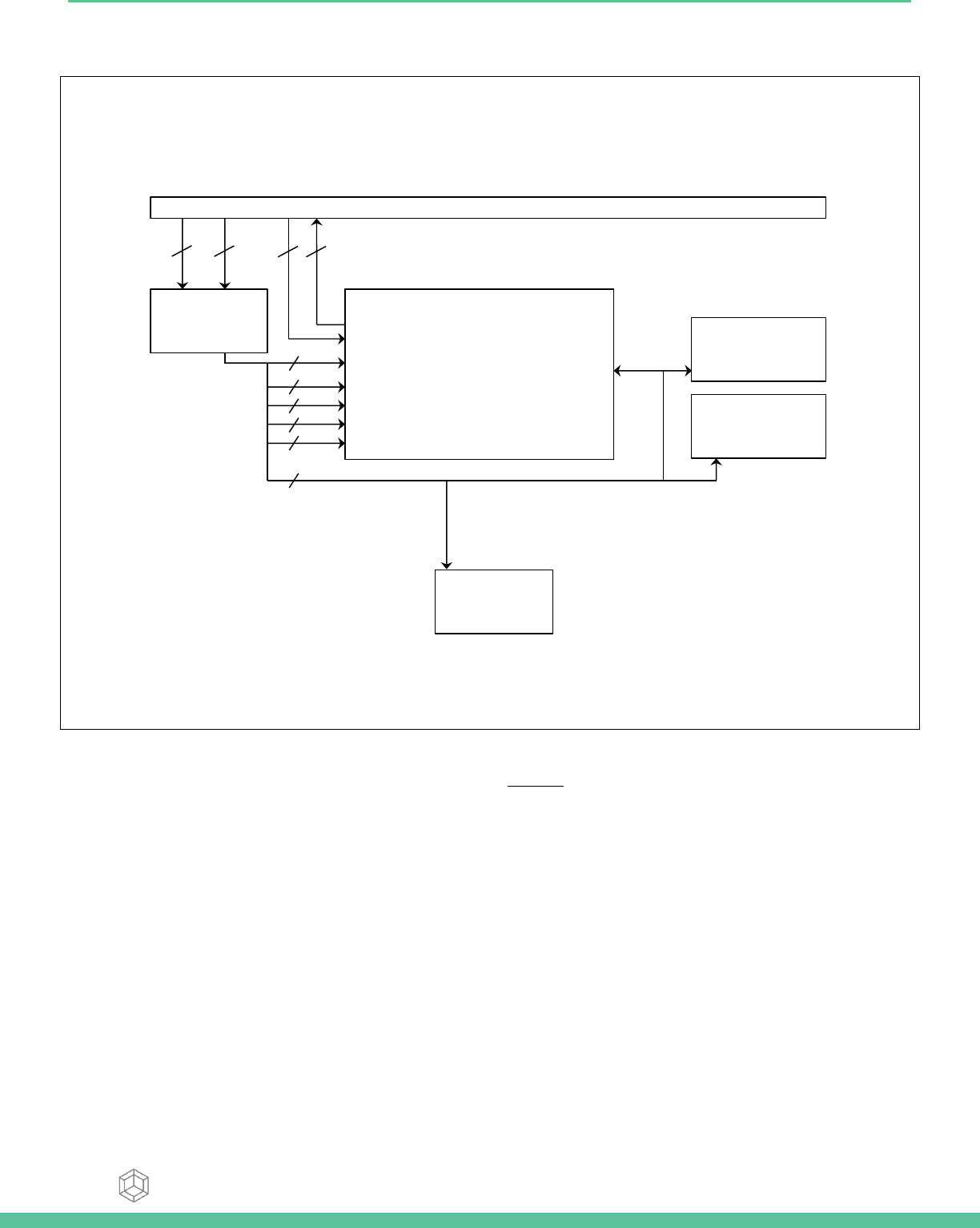
The main SoC on the ARTIK 050 Module is based on the BCM43907 from Broadcom Ltd. Figure 2 shows the
block schematic of the SoC.
The system is architected with 2 dedicated Cortex-R4 cores. The first Cortex-R4 core, running at 160MHz, is solely responsible
for WLAN activities. It contains 512KB of Tightly-Coupled (TC) RAM in addition to 320KB of TC ROM.
The tight coupling assures that the WLAN functionality can operate fully autonomously.
The second core, also a Cortex-R4, is specifically added for application processing. The core is supported by 2MB
of SRAM for application code. The core can run in 2 speed modes. The 160MHz mode is available when conserving power is
important, while the 320MHz mode can be used when more intensive processing is required.
In addition to the dual core Cortex-R4, there is a wide array of interfaces available. The ARTIK 050 Module has 2x UART (2-pin),
2x I2C, 11x GPIO (dedicated) + 5x GPIO (shared between JTAG), 6x PWM, 1x 4-pin I2S (No Data In), 1x 5-pin I2S, 2x SPI, 2x I2C, 1x
USB and 1x JTAG (that shared 5 GPIO pins) interface for debugging and bring-up activities.
The great variety of interfaces makes the ARTIK 050 Module the right module for a wide variety of IoT markets.
Samsung Semiconductor, Inc. ARTIK 050 Module Data Sheet
Samsung Confidential
Specifications in this document are tentative and subject to
change.
9
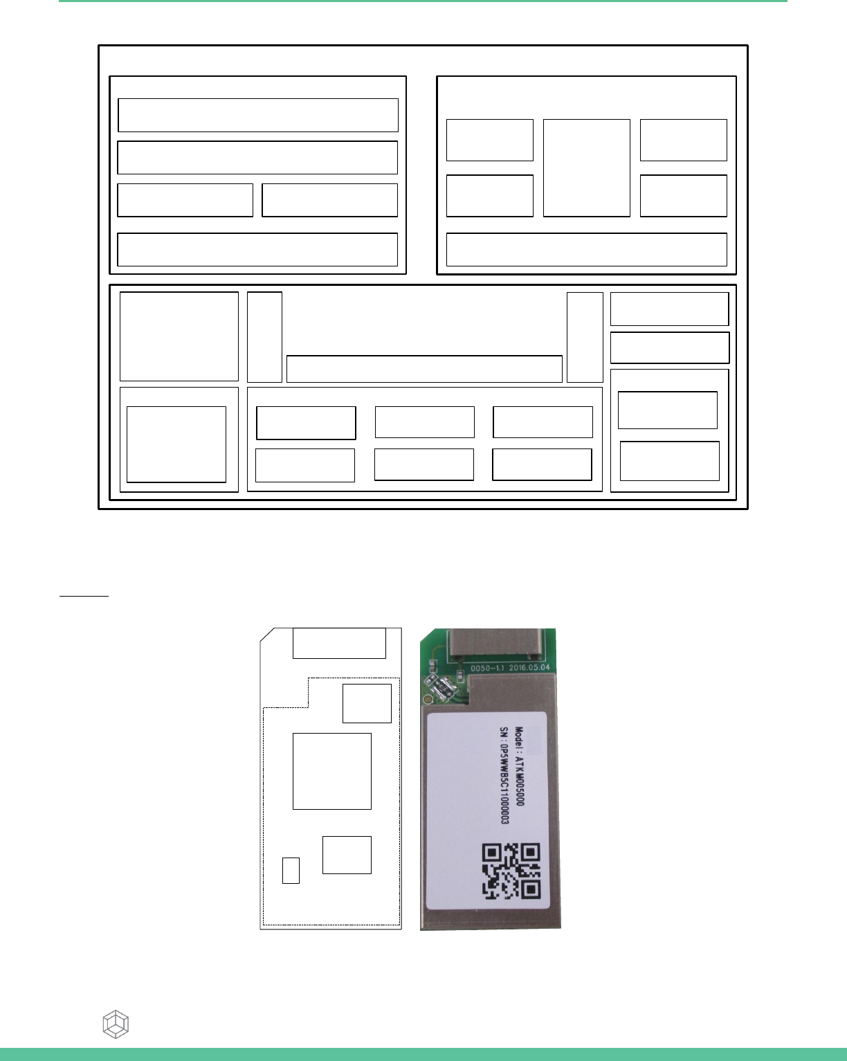
Figure 2. ARTIK 050 Module Main SoC Block Diagram
Figure 3 shows the top side of the ARTIK 050 Module that is populated with the ARM application processor, the flash memory,
the Secure Element and the Level Shifter.
Figure 3. ARTIK 050 Module – Top View
BCM43907
CORTEX-R4
32KB I-CACHE
32KB D-CACHE
Peripherals
GPIO JTAG
SPI|BSC
High Speed I/F
USB 2.0
BSC PWM
UART
Multi Media
AUDIO
I2S
2MB RAM
640KB ROM
CRYPTOGRAPHY
APPS DOMAIN
ALWAYS ON DOMAIN WLAN DOMAIN
AXI BRIDGE
AXI BRIDGE AXI BRIDGE
PS RAMRTC
PMU CONTROLLER
PMU
CORTEX-R4
IEEE 802.11 MAC
IEEE 802.11n PHY
2.4GHz RADIO
512KB RAM
320KB ROM
AXI BRIDGE
AXI BRIDGE
PROCESSOR
BCM43907
FLASH
MX25L6433F
SECURE
ELEMENT
S3FT9MF
LEVEL
SHIFTER
2N7002DW
STRUCTURAL ANTENNA
WSANT2G01
Samsung Semiconductor, Inc. ARTIK 050 Module Data Sheet
Samsung Confidential
Specifications in this document are tentative and subject to
change.
10
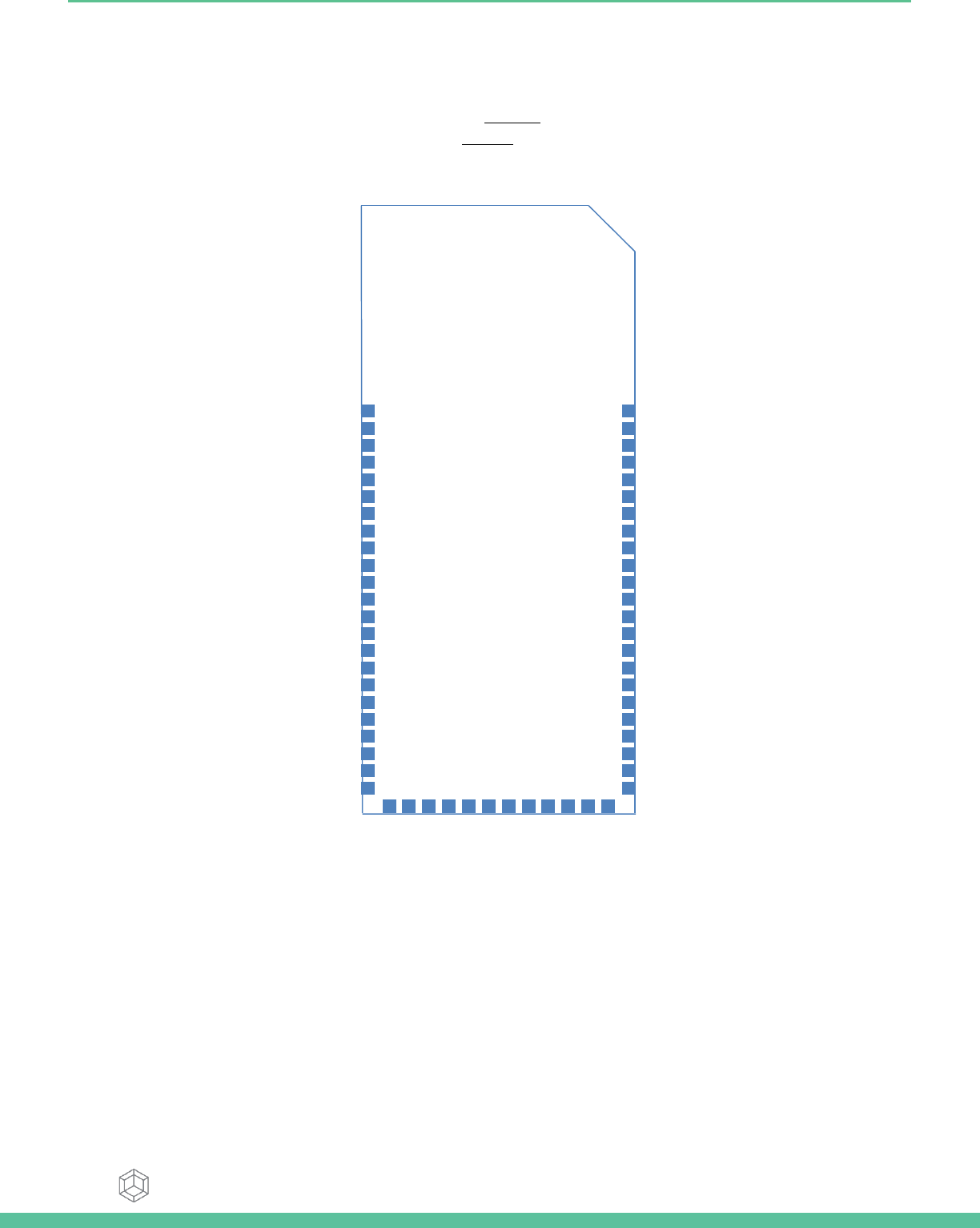
ARTIK 050 MODULE PADS
The ARTIK 050 Module utilizes 58 individual PADS straight on the PCB. The 58 individual PADS provide Power, GND, RESET,
GPIO, PWM, I2C, I2S, SPI, JTAG, UART and USB functionality. In Figure 4, logical listing is provided of all power/signal names
that are assigned to physical pins of the PADS. In addition, Table 1 provides an in depth description of the functionality of
each signal available on the PADS.
Figure 4. ARTIK 050 Module PADs Bottom View
35 34 33 32 31 30 29 28 27 26 25 24
GPIO_15_HOST_VTRIM
GPIO_16
VIN
I2S0_MCK
I2S_SCK_BCLK
I2S_SD_OUT
I2S0_WS_LRCLK
PWR_RST
SPI_0_CLK
SPI_0_MOSI
SPI_0_MISO
GND
GPIO_13_SDIO_MODE
I2C_0_SCL
I2C_0_SDA
GPIO_0
PWM_5
PWM_4
PWM_3
PWM_2
PWM_0
GND
GPIO_8_TAP_SEL
GPIO_9_USB_HSIC_SEL
GPIO_11_ACPU_BOOT_MODE
GND
GPIO_12
GPIO_14
GPIO_7_WCPU_BOOT_MODE
USB2_DN
USB2_DP
GND
UART_TXD
UART_RXD
PWM_1
1
2
3
4
5
6
7
8
9
10
11
12
13
14
15
16
17
18
19
20
21
22
23
RESET_N
GND
GPIO_6_JTAG_TRST_L
GPIO_5_JTAG_TDO
GPIO_4_JTAG_TDI
GPIO_3_JTAG_TMS
GPIO_2_JTAG_TCK
SPI_1_CLK
SPI_1_MISC
3.3V_OUT
SPI_1_MOSI
I2S1_MCK
I2S1_SCK_BCLK
I2S1_SD_IN
I2S1_SD_OUT
I2S1_WS_LRCLK
I2C_1_SDA
I2C_1_SCL
SPI_1_CS
RF_SW_CTRL_6_UART1_RX_IN
RF_SW_CTRL_7_RSRC_INIT_MODE_ART1_TX_OUT
SPI_0_CS
GPIO_1_GSPI_MODE 58
57
56
55
54
53
52
51
50
49
48
47
46
45
44
43
42
41
40
39
38
37
36
ARTIK 050 MODULE
BOTTOM VIEW
Samsung Semiconductor, Inc. ARTIK 050 Module Data Sheet
Samsung Confidential
Specifications in this document are tentative and subject to
change.
11
Table 1. PAD Description
PAD
#
Name
Voltage
[V]
I/O
Type
DF
Active
Mode
Low
Power
Mode
Power
Down
Mode
DS
[mA]
Default
Function
Comments
Comments
for Design
1
I2C_0_SCL
3V35
BCM
I/O
PU
-
-
-
-
-
I2C0 CLK
Internal 4.7K /
3.3V Pull-up
2
I2C_0_SDA
3V35
BCM
I/O
PU
-
-
-
-
-
I2C0 DATA
Internal 4.7K /
3.3V Pull-up
3
PWM_5
3V35
BCM
I/O
-
-
-
-
-
-
PWM 5
4
PWM_4
3V35
BCM
I/O
-
-
-
-
-
-
PWM 4
5
PWM_3
3V35
BCM
I/O
-
-
-
-
-
-
PWM 3
6
PWM_2
3V35
BCM
I/O
-
-
-
-
-
-
PWM 2
7
PWM_0
3V35
BCM
I/O
-
-
-
-
-
-
PWM 0
8
PWM_1
3V35
BCM
I/O
-
-
-
-
-
-
PWM 1
9
GPIO_0
3V35
BCM
I/O
IN/PD
IO/PU/P
D/NP
IO/PU/PD/N
P
High-Z/NP
8
USB20H_CTL
GPIO 0
For USB mode,
need to connect
overcurrent flag
pin with 4.7K
Pull-up
10
GND
0V0
NA
NA
NA
NA
NA
NA
NA
Ground
11
USB2_DN
3V35
BCM
USB
-
-
-
-
-
-
USB2_DN
12
USB2_DP
3V35
BCM
USB
-
-
-
-
-
-
USB2_DP
13
GND
0V0
NA
NA
NA
NA
NA
NA
NA
Ground
14
GPIO_7_WCPU_B
OOT_MODE
3V35
BCM
I/O
IN/PU
IO/PU/P
D/NP
IO/PU/PD/N
P
High-Z/NP
8
-
Boot Wireless
CPU from
Tightly Coupled
RAM
Internal 10K/3.3V
Pull-up for boot
mode : not
recommended
Pull down
resistor
15
GPIO_8_TAP_SEL
3V35
BCM
I/O
IN/PU
IO/PU/P
D/NP
IO/PU/PD/N
P
High-Z/NP
8
GPIO_8
GPIO 8, default
function
TAP_SEL_P
Internal 10K/3.3V
Pull-up for boot
mode : not
recommended
Pull-down
resistor
Only fo Input,
Not support
Output
16
GPIO_9_USB_HSI
C_SEL
3V35
BCM I
IN/PU
IO/PU/P
D/NP
IO/PU/PD/N
P
High-Z/NP
8
GPIO_9
USB 2.0 PHY is
selected
Internal 10K/3.3V
Pull-up for boot
mode : not
recommended
Pull-down
resistor
17
GPIO_11_ACPU_B
OOT_MODE
3V35
BCM
I/O
IN/PD
IO/PU/P
D/NP
IO/PU/PD/N
P
High-Z/NP
8
-
Boot Main CPU
from internal
ROM
For boot mode :
not
recommended
Pull-up resistor
18
UART_TXD
3V35
BCM
UART
(LS)
-
-
-
-
-
-
Level Shifted
UART_TXD
Level Shifted
UART_TXD, need
to Pull-up
resistor for UART
communication
Samsung Semiconductor, Inc. ARTIK 050 Module Data Sheet
Samsung Confidential
Specifications in this document are tentative and subject to
change.
12
PAD
#
Name
Voltage
[V]
I/O
Type
DF
Active
Mode
Low
Power
Mode
Power
Down
Mode
DS
[mA]
Default
Function
Comments
Comments
for Design
19
UART_RXD
3V35
BCM
UART
(LS)
-
-
-
-
-
-
Level Shifted
UART_RXD
Level Shifted
UART_RXD, need
to Pull-up
resistor for UART
communication
1K serial resistor
after Level-
shifter, not
recommended
serial resister
over 1K
20
GND
0V0
NA
NA
NA
NA
NA
NA
NA
Ground
21
GPIO_12
3V35
BCM
I/O
IN/NP
IO/PU/P
D/NP
IO/PU/PD/N
P
High-Z/NP
8
GPIO_12
GPIO 12
22
GPIO_14
3V35
BCM
I/O
IN/NP
IO/PU/P
D/NP
IO/PU/PD/N
P
High-Z/NP
8
GPIO_14
GPIO 14
23
GPIO_13_SDIO_M
ODE
3V35
BCM
I/O
IN/PU
IO/PU/P
D/NP
IO/PU/PD/N
P
High-Z/NP
8
-
GPIO 13 boot
strap
SDIO_MODE
Internal 10K/3.3V
Pull-up for boot
mode : not
recommended
Pull up resistor
24
GPIO_15_HOST_V
TRIM
3V35
BCM
I/O
IN/PD
IO/PU/P
D/NP
IO/PU/PD/N
P
High-Z/NP
8
-
GPIO 15 boot
strap VTRIM_EN
for boot mode :
not
recommanded
Pull-up resistor
25
GPIO_16
3V35
BCM
I/O
IN/NP
IO/PU/P
D/NP
IO/PU/PD/N
P
High-Z/NP
8
-
GPIO 16
26
I2S0_MCK
3V35
BCM
I/O
-
-
-
-
-
-
I2S 0 MCK
27
I2S0_SCK_BLCK
3V35
BCM
I/O
-
-
-
-
-
-
I2S 0 SCK_BLCK
28
I2S0_SD_OUT
3V35
BCM
I/O
-
-
-
-
-
-
I2S 0 SD_OUT
29
I2S0_WS_LRCLK
3V35
BCM
I/O
-
-
-
-
-
-
I2S 0 WS_LRCLK
30
PWR_RST
NA
Power
En
Input
-
-
-
-
-
-
if PWR_RST is 0
DCDC disabled
150Kohm PU,
75Kohm PD, VIH
1.45V, VIL 0.4V
31
GND
0V0
NA
NA
NA
NA
NA
NA
NA
Ground
Ground
32
VIN
4V5
Power
Input
NA
NA
NA
NA
NA
NA
Power
MIN 4.75 ~ MAX
18V
33
SPI_0_CLK
3V35
BCM
I/O
-
-
-
-
-
-
SPI 0 CLK
34
SPI_0_MOSI
3V35
BCM
I/O
-
-
-
-
-
-
SPI 0 MOSI
35
SPI_0_MISO
3V35
BCM
I/O
-
-
-
-
-
-
SPI 0 MISO
36
SPI_0_CS
3V35
BCM
I/O
-
-
-
-
-
-
SPI 0 CS
37
3.3V_OUT
3V35
NA
NA
NA
NA
NA
NA
NA
Power
Power pin for
050 IO port,
Current limit
100mA @3.3V
38
RESET_N
3V35
BCM
RESET
-
-
-
-
-
-
Reset ARTIK 050
Module
Reset pin, not
recommended
Pull-down
resister
39
GPIO_3_JTAG_TM
S
3V35
BCM
I/O
IN/PD
IO/PU/P
D/NP
IO/PU/PD/N
P
High-Z/NP
8
GCI_GPIO(1)
Debug_JTAG
40
GPIO_4_JTAG_TDI
3V35
BCM
I/O
IN/NP
IO/PU/P
D/NP
IO/PU/PD/N
P
High-Z/NP
8
GCI_GPIO(2)
Debug_JTAG
Samsung Semiconductor, Inc. ARTIK 050 Module Data Sheet
Samsung Confidential
Specifications in this document are tentative and subject to
change.
13
PAD
#
Name
Voltage
[V]
I/O
Type
DF
Active
Mode
Low
Power
Mode
Power
Down
Mode
DS
[mA]
Default
Function
Comments
Comments
for Design
41
GPIO_2_JTAG_TC
K
3V35
BCM
I/O
NP
IO/PU/P
D/NP
IO/PU/PD/N
P
High-Z/NP
8
GCI_GPIO(0)
Debug_JTAG
42
GPIO_5_JTAG_TD
O
3V35
BCM
I/O
IN/PD
IO/PU/P
D/NP
IO/PU/PD/N
P
High-Z/NP
8
GCI_GPIO(3)
Debug_JTAG
43
GPIO_6_JTAG_TRS
T_L
3V35
BCM
I/O
IN/NP
IO/PU/P
D/NP
IO/PU/PD/N
P
High-Z/NP
8
GCI_GPIO(4)
Debug_JTAG
44
GND
0V0
NA
NA
NA
NA
NA
NA
NA
Ground
45
RF_SW_CTRL_6_U
ART1_RX_IN
3V35
BCM
I/O
OUT/NP
O/NP
O/NP
High-Z
-
-
RF_SW+CTRL_6
Debug_UART_RX
46
RF_SW_CTRL_7_R
SRC_INIT_MODE_
UART1_TX_OUT
3V35
BCM
I/O
IN/PD
O/NP
O/NP
High-Z
-
-
RF_SW+CTRL_7
PMU enable strap
Debug_UART_TX
47
I2C_1_SCL
3V35
BCM
I/O
PU
-
-
-
-
-
I2C 1 SCL
Internal
4.7K/3.3V Pull-up
48
I2C_1_SDA
3V35
BCM
I/O
PU
-
-
-
-
-
I2C 1 SDA
Internal
4.7K/3.3V Pull-up
49
I2S1_WS_LRCLK
3V35
BCM
I/O
-
-
-
-
-
-
I2S 1 WS_LRCLK
50
I2S1_SD_OUT
3V35
BCM
I/O
-
-
-
-
-
-
I2S 1 SD_OUT
51
I2S1_SD_IN
3V35
BCM
I/O
-
-
-
-
-
-
I2S 1 SD_IN
52
I2S1_SCK_BCLK
3V35
BCM
I/O
-
-
-
-
-
-
I2S 1 SCK_BCLK
53
I2S1_MCK
3V35
BCM
I/O
-
-
-
-
-
-
I2S 1 MCK
54
SPI_1_MOSI
3V35
BCM
I/O
-
-
-
-
-
-
SPI 1 MOSI
55
SPI_1_CS
3V35
BCM
I/O
-
-
-
-
-
-
SPI 1 CS
56
SPI_1_MISO
3V35
BCM
I/O
-
-
-
-
-
-
SPI 1 MISO
57
SPI_1_CLK
3V35
BCM
I/O
-
-
-
-
-
-
SPI 1 CLK
58
GPIO_1_GSPI_MO
DE
3V35
BCM
I/O
NP
IO/PU/P
D/NP
IO/PU/PD/N
P
High-Z/NP
8
-
GPIO 1 with
GSPI_MODE
strap
For boot mode :
not
recommended
Pull-up resistor
*PU = Pull Up, PD = Pull Down, NP = No Pull
Samsung Semiconductor, Inc. ARTIK 050 Module Data Sheet
Samsung Confidential
Specifications in this document are tentative and subject to
change.
14
ARTIK 050 MODULE GPIO ALTERNATE FUNCTIONS
All the GPIOs, as indicated in Table 1, have alternate functions that can be programmed using the GPIO API provided in the
SW development environment. In Table 2 and Table 3, the alternate functions of all GPIOs connected only to the BCM43907
that are available on the PADS of the ARTIK 050 Module are described.
Table 2. GPIO Alternate Functions
PAD
#
Name
DF
F1
F2
F3
F4
F5
1
I2C_0_SCL
-
I2C0_CLK
GPIO_22
GPIO_29
-
-
2
I2C_0_SDA
-
I2C0_SDATA
GPIO_21
GPIO_28
-
-
3
PWM_5
-
PWM5
GPIO_8
GPIO_23
-
-
4
PWM_4
-
PWM4
GPIO_6
GPIO_22
-
-
5
PWM_3
-
PWM3
GPIO_5
GPIO_21
-
-
6
PWM_2
-
PWM2
GPIO_4
GPIO_20
-
-
7
PWM_0
-
PWM0
GPIO_2
GPIO_18
-
-
8
PWM_1
-
PWM1
GPIO_3
GPIO_19
-
-
9
GPIO_0
USB20H_CT
L
GPIO_0
UART0_RXD
I2C1_SDATA
PWM0
SPI1_MISO
14
GPIO_7_WCPU_BOOT_MODE
-
GPIO_7
UART0_RTS_OU
T
PWM1
PWM3
SPI1_CS
15
GPIO_8_TAP_SEL
GPIO_8
GPIO_8
SPI1_MISO
PWM2
PWM4
UART0_RXD
16
GPIO_9_USB_HSIC_SEL
GPIO_9
GPIO_9
SPI1_CLK
PWM3
PWM5
UART0_TXD
17
GPIO_11_ACPU_BOOT_MODE
-
GPIO_11
SPI1_CS
PWM5
I2C1_CLK
UART0_RTS_OU
T
21
GPIO_12
GPIO_12
GPIO_12
I2C1_SDATA
UART0_RXD
SPI1_MISO
PWM2
22
GPIO_14
GPIO_14
GPIO_14
PWM0
UART0_CTS_IN
SPI1_MOSI
I2C1_SDATA
23
GPIO_13_SDIO_MODE
-
GPIO_13
I2C1_CLK
UART0_TXD
SPI1_CLK
PWM3
24
GPIO_15_HOST_VTRIM
-
GPIO_15
PWM1
UART0_RTS_OU
T
SPI1_CS
I2C1_CLK
25
GPIO_16
-
GPIO_16
UART0_CTS_IN
PWM0
PWM2
SPI1_MOSI
26
I2S0_MCK
-
I2S_MCLK0
GPIO_23
GPIO_0
-
-
27
I2S0_SCK_BLCK
-
I2S_SCLK0
GPIO_24
GPIO_2
-
-
28
I2S0_SD_OUT
-
I2S_SDATAO0
GPIO_27
GPIO_5
-
-
29
I2S0_WS_LRCLK
-
I2S_LRCLK0
GPIO_25
GPIO_3
-
-
33
SPI_0_CLK
-
SPI0_CLK
GPIO_18
GPIO_25
-
-
34
SPI_0_MOSI
-
SPI0_MOSI
GPIO_19
GPIO_26
-
-
35
SPI_0_MISO
-
SPI0_MISO
GPIO_17
GPIO_24
-
-
36
SPI_0_CS
-
SPI0_CS
GPIO_20
GPIO_27
-
-
39
GPIO_3_JTAG_TMS
GCI_GPIO(1)
GPIO_3
-
-
GCI_GPIO_
1
-
40
GPIO_4_JTAG_TDI
GCI_GPIO(2)
GPIO_4
-
-
GCI_GPIO_
2
-
41
GPIO_2_JTAG_TCK
GCI_GPIO(0)
GPIO_2
-
-
GCI_GPIO_
0
-
42
GPIO_5_JTAG_TDO
GCI_GPIO(3)
GPIO_5
-
-
GCI_GPIO_
3
-
43
GPIO_6_JTAG_TRST_L
GCI_GPIO(4)
GPIO_6
-
-
GCI_GPIO_
4
-
45
RF_SW_CTRL_6_UART1_RX_IN
-
RF_SW+CTRL_
6
UART_DBG_RX
SECI_IN
-
-

Samsung Semiconductor, Inc. ARTIK 050 Module Data Sheet
Samsung Confidential
Specifications in this document are tentative and subject to
change.
15
PAD
#
Name
DF
F1
F2
F3
F4
F5
46
RF_SW_CTRL_7_RSRC_INIT_
MODE_UART1_TX_OUT
-
RF_SW+CTRL_
7
UART_DBG_TX
SECI_OUT
-
-
49
I2S1_WS_LRCLK
-
I2S_LRCLK1
GPIO_0
GPIO_31
-
-
50
I2S1_SD_OUT
-
I2S_SDATAO1
GPIO_28
GPIO_6
-
-
51
I2S1_SD_IN
-
I2S_SDATAI1
GPIO_29
GPIO_8
-
-
52
I2S1_SCK_BCLK
-
I2S_SCLK1
GPIO_31
GPIO_30
-
-
53
I2S1_MCK
-
I2S_MCLK1
GPIO_30
GPIO_17
-
-
58
GPIO_1_GSPI_MODE
-
GPIO_1
UART0_TXD
I2C1_CLK
PWM1
SPI1_CLK
Samsung Semiconductor, Inc. ARTIK 050 Module Data Sheet
Samsung Confidential
Specifications in this document are tentative and subject to
change.
16
Table 3. GPIO Alternate Functions (continued)
PAD
#
Name
F6
F7
F8
F9
F10
F11
1
I2C_0_SCL
-
-
-
-
-
-
2
I2C_0_SDA
-
-
-
-
-
-
3
PWM_5
-
-
-
-
-
-
4
PWM_4
-
-
-
-
-
-
5
PWM_3
-
-
-
-
-
-
6
PWM_2
-
-
-
-
-
-
7
PWM_0
-
-
-
-
-
-
8
PWM_1
-
-
-
-
-
-
9
GPIO_0
PWM2
GPIO_12
GPIO_8
-
PWM4
USB20H_CTL
14
GPIO_7_WCPU_BOOT_MODE
I2C1_CLK
GPIO_15
GPIO_11
PMU_TEST_O
-
PWM5
15
GPIO_8_TAP_SEL
-
GPIO_16
GPIO_12
TAP_SEL_P
I2C1_SDAT
A
PWM0
16
GPIO_9_USB_HSIC_SEL
-
GPIO_0
GPIO_13
-
I2C1_CLK
PWM1
17
GPIO_11_ACPU_BOOT_MODE
PWM1
GPIO_7
GPIO_15
PWM3
-
-
21
GPIO_12
PWM4
GPIO_8
GPIO_16
PWM0
SDIO_SEP_
INT_0D
SDIO_SEP_INT
22
GPIO_14
-
GPIO_10
-
PWM4
-
PWM2
23
GPIO_13_SDIO_MODE
PWM5
GPIO_9
GPIO_0
PWM1
-
-
24
GPIO_15_HOST_VTRIM
-
GPIO_11
GPIO_7
PWM5
-
PWM3
25
GPIO_16
I2C1_SDATA
GPIO_14
GPIO_10
RF_DISABLE_L
-
PWM4
26
I2S0_MCK
-
-
-
-
-
-
27
I2S0_SCK_BLCK
-
-
-
-
-
-
28
I2S0_SD_OUT
-
-
-
-
-
-
29
I2S0_WS_LRCLK
-
-
-
-
-
-
33
SPI_0_CLK
-
-
-
-
-
-
34
SPI_0_MOSI
-
-
-
-
-
-
35
SPI_0_MISO
-
-
-
-
-
-
36
SPI_0_CS
-
-
-
-
-
-
39
GPIO_3_JTAG_TMS
-
-
-
TMS
-
-
40
GPIO_4_JTAG_TDI
-
-
-
TDI
-
-
41
GPIO_2_JTAG_TCK
-
-
-
TCK
-
-
42
GPIO_5_JTAG_TDO
-
-
-
TDO
-
-
43
GPIO_6_JTAG_TRST_L
-
-
-
TRST_L
-
-
45
RF_SW_CTRL_6_UART1_RX_IN
-
-
-
-
-
-
46
RF_SW_CTRL_7_RSRC_INIT_
MODE_UART1_TX_OUT
-
-
-
-
-
-
49
I2S1_WS_LRCLK
-
-
-
-
-
-
50
I2S1_SD_OUT
-
-
-
-
-
-
51
I2S1_SD_IN
-
-
-
-
-
-
52
I2S1_SCK_BCLK
-
-
-
-
-
-
53
I2S1_MCK
-
-
-
-
-
-
58
GPIO_1_GSPI_MODE
PWM3
GPIO_13
GPIO_9
-
PWM5
-

Samsung Semiconductor, Inc. ARTIK 050 Module Data Sheet
Samsung Confidential
Specifications in this document are tentative and subject to
change.
17
ARTIK 050 MODULE BOOTING PROCESS
When booting the ARTIK 050 Module, various strapping options are used to guarantee a certain booting behavior.
In addition, some GPIOs are set to perform alternate functions instead of their default boot-up behavior. The following
summary provides a list reflecting what strapping options were used and what states certain GPIOs will attain:
Boot Wireless CPU from tightly coupled RAM using GPIO_7_WCPU_BOOT_MODE as high during boot
Boot main CPU from internal ROM using GPIO_11_ACPU_BOOT_MODE as low during boot
Set GPIO_8_TAP_SEL in TAP_SEL_P default mode
Enable USB 2.0 PHY using GPIO_9_USB_HSIC_SEL as high during boot
Enable PMU resource initialization mode selection using RF_SW_CTRL_7_RSRC_INIT_MODE_UART1_TX_OUT
as low during boot
Set RF_SW_CTRL_6_UART1_RX_IN in UART_DBG_RX default mode
Set GPIO_2_JTAG_TCK as JTAG_TCK default mode
Set GPIO_3_JTAG_TMS as JTAG_TMS default mode
Set GPIO_4_JTAG_TDI as JTAG_TDI default mode
Set GPIO_5_JTAG_TDO as JTAG_TDO default mode
Set GPIO_6_JTAG_TRST_L as JTAG_TRST_L default mode
Once the boot is completed, most of the GPIO pins that are not set for alternate functions can be used as generic GPIOs. In
addition, the GPIO pins can always be reprogrammed to functions that serve the product’s design needs.
Samsung Semiconductor, Inc. ARTIK 050 Module Data Sheet
Samsung Confidential
Specifications in this document are tentative and subject to
change.
18
ARTIK 050 MODULE ELECTRICAL SPECIFICATIONS
ABSOLUTE MAXIMUM RATINGS
Absolute maximum ratings are those ratings where permanent damage to the ARTIK 050 Module can occur.
Functional operation at absolute maximum ratings is not guaranteed and not recommended.
Table 4. Absolute Maximum Ratings
PAD:[Pin#]
Symbol
Condition
Min
Typ
Max
Units
PAD:[32]
VIN
Input voltage VIN on the high efficiency step down
converter (IM8123SM)
–
–
20
V
PAD:[1,2,3,4,5,6,7,8,9,14,15,
16,17,21,22,23,24,25,26,27,
28,29,33,34,35,36,39,40,
41,42,43,45,46,47,48,49,50,
51,52,53,54,55,56,57,58]
Vundershoot
Undershoot voltage for I/O
-0.50
–
–
V
PAD:[30]
PWR_RST
–
-0.30
–
20.3
V
PAD:[18,19]
VMAX
IO is running at 3.3V level shifter is closed so 60+3.3
–
–
63.3
V
IMAX
Continuous
–
–
115
mA
Continuous at 100°C
–
–
73
mA
Pulsed
–
–
800
mA
RECOMMENDED OPERATING CONDITIONS
The following table describes the operating conditions of the ARTIK 050 Module:
Table 5. Recommended Operating Conditions
PAD:[Pin#]
Symbol
Condition
Min
Typ
Max
Units
PAD:[32]
VIN
Input voltage VIN on the high efficiency
step down converter (IM8123SM)
4.50
–
18.0
V
–
TO
Maximum operating temperature
-25
–
85
°C
TS
Storage temperature
-40
–
125
°C
Samsung Semiconductor, Inc. ARTIK 050 Module Data Sheet
Samsung Confidential
Specifications in this document are tentative and subject to
change.
19
POWER SUPPLY REQUIREMENTS
Figure 5. ARTIK 050 Module Power Distribution
The power management of the ARTIK 050 Module, as depicted in Figure 5, contains the IM8123SN high-efficiency
DC-DC convertor that will handle all power requirements for the ARTIK 050 Module.
BCM43907
MX25L6433F
8MB FLASH
S3FT9MF
SE
58 PADS
2N7002DW
LEVEL
SHIFTER
5
GND
VDD_VBAT
1
IM8123SN
DC-DC
VIN
VDDIO
USB_VDD_3V3
1
VDDIO_RMII
1
VDDIO_AUDIO
1
VDDIO_SD
1
1
1
GND
VDDIO
3V3 VDDIO
1
VDDIO
1
PWR_RST
Samsung Semiconductor, Inc. ARTIK 050 Module Data Sheet
Samsung Confidential
Specifications in this document are tentative and subject to
change.
20
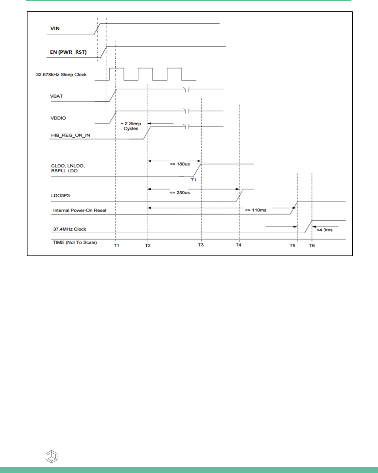
Figure 6. ARTIK 050 Module Power Sequence
Note : The BCM43907 has an internal power-on reset (POR) circuit. The device will be held in reset for a maximum of 110 ms after VDDC and
VDDIO have both passed the POR threshold.
Note : The 10%-90% VBAT rise time should not be faster than 40µ s. VBAT should be up before or at the same time as VDDIO. VDDIO should
not be present first or be held high before VBAT is high.

Samsung Semiconductor, Inc. ARTIK 050 Module Data Sheet
Samsung Confidential
Specifications in this document are tentative and subject to
change.
21
ESD RATINGS
Table 6. ESD Ratings
Parameter
Min
Typ
Max
Units
ESD stress voltage Human Body Model
-1.0
–
1.0
kV
ESD stress voltage Charged Device Model
–
250
–
V
Samsung Semiconductor, Inc. ARTIK 050 Module Data Sheet
Samsung Confidential
Specifications in this document are tentative and subject to
change.
22
DC ELECTRICAL CHARACTERISTICS
Table 7 below describes the DC characteristics for all GPIO pins that are available on the PAD.
Table 7.I/O DC Characteristics
PAD:[Pin#]
Symbo
l
Condition
Min
Typ
Max
Unit
s
PAD:[1,2,3,4,5,6,7,8,9,14,
15,16,17,21,22,23,24,25,
26,27,28,29,33,34,35,
36,39,40,41,42,43,45,46,
47,48,49,50,51,52,53,54,
55,56,57,58]
VIH
Input high voltage
2.00
–
–
V
VIL
Input low voltage
–
–
0.80
V
VOH
Output high voltage @ 2mA
2.90
–
–
V
VOL
Output low voltage @ 2mA
–
–
0.40
V
PAD:[19]
VIH
Input high voltage
3.5
5
20
V
VIL
Input low voltage
–
–
0.2
V
PAD:[45,46]*
CIN
Input capacitance
–
–
5
pF
*Programmable 2mA to 16mA drive strength. The default is 10mA.
Samsung Semiconductor, Inc. ARTIK 050 Module Data Sheet
Samsung Confidential
Specifications in this document are tentative and subject to
change.
23
AC ELECTRICAL CHARACTERISTICS
This section describes the timing and its associated constraints on the various interfaces (I2C, I2S, etc.) that can be found on
the PAD.
I2S TX TIMING DIAGRAM
Figure 7. I2S Tx Timing Diagram
I2S RX TIMING DIAGRAM
Figure 8. I2S Rx Timing Diagram
I2S_SCLK
I2S_SDATAO
and I2S_LRCK
tdtr = 0.8T
T
thtr = 0
tRC
tHC = 0.35T
tLC = 0.35TVH = 2.0V
VL = 0.8V
T = Clock Period
Ttr = Minimum allowed Clock Period for transmitter
T > Ttr
tRC is only relevant for transmitters in Slave mode
I2S_SCLK
I2S_SDATAI
and I2S_LRCK
tsr = 0.2T
TtHC = 0.35T
tLC = 0.35TVH = 2.0V
VL = 0.8V
T = Clock Period
Tr = Minimum allowed Clock Period for transmitter
T > Tr
thr = 0
Samsung Semiconductor, Inc. ARTIK 050 Module Data Sheet
Samsung Confidential
Specifications in this document are tentative and subject to
change.
24
I2S RECEIVER/TRANSMITTER TIMING PARAMETERS
Table 8. I2S Tx/Rx Timing Parameters
Parameter
Transmitter
Receiver
Lower Limit
Upper Limit
Lower Limit
Minimu
m
Maximu
m
Minimu
m
Maximu
m
Minimu
m
Maximu
m
Clock Period T
Ttr
–
–
–
Ttr
–
Slave Mode:
–
Clock HIGH, tHC
–
0.35Tr
–
–
–
0.35Tr
Clock LOW, tLC
–
0.35Tr
–
–
–
0.35Tr
Clock rise time, tRC
–
–
0.15Tr
–
–
–
Transmitter Delay, tdtr
–
–
–
0.8T
–
–
Transmitter Hold Time, thtr
0
–
–
–
–
–
Receiver Setup Time, tsr
–
–
–
–
–
0.2Tr
Receiver Hold Time, thr
–
–
–
–
–
0
Table 9. I2S M_CLK Specification
Parameter
Minimu
m
Typica
l
Maximu
m
Unit
Frequency Range
1
–
40
MHz
Frequency Accuracy (with respect to the XTAL frequency)
–
1
–
ppb
Tuning Resolution
–
50
–
ppb
Tuning Range
–
1000
–
ppm
Tuning Step Size
–
–
10
ppm
Tuning Rate
–
1
–
ppm/ms
Baseband Jitter (100Hz–40kHz)
–
–
100
ps rms
Wideband Jitter (100Hz–1MHz)
–
–
200
ps rms
I2S FRAME LEVEL TIMING
Figure 9. I2S Frame Level Timing
I2S_SCLK
I2S_LRCLK
1 clock
I/O Data 1 2 3
MSB
1 clock
n-2 nn-1
LSB
1 2 3
MSB
n-2 nn-1
LSB
1/fs
Left Channel Right Channel
Samsung Semiconductor, Inc. ARTIK 050 Module Data Sheet
Samsung Confidential
Specifications in this document are tentative and subject to
change.
25
USB PHY TIMING DIAGRAMS
Figure 10. USB2.0 Bus Reset to High-Speed Mode Operation
Figure 11. USB2.0 High Speed Mode Transmit Timing
DM Idle
DP Idle
< 100 µs
40 to 60 µs
100 to 500 µs
HS Data
HS Data
> 1.0 ms3 to 3.125 ms
Device
K-Chirp
100 to
875 µs
< 7 ms
> 10 ms
Start of
Reset
Device goes
into Full-
Speed Mode
Start of Host
(Hub) Chirp
Device Tests for Single-Ended
Zero (SE0 State)
End of Host
(Hub) Chirp
End of
Reset
High-Speed
Chirp
CLK60
TXDATA
DP/DM
TXVALID
TXREADY
XVERSEL
OPMODE
TERMSEL
00
00
0
B0 B1PID
Latency = 42 bits
96 bits
Tx driver is
enabled here
Samsung Semiconductor, Inc. ARTIK 050 Module Data Sheet
Samsung Confidential
Specifications in this document are tentative and subject to
change.
26
Figure 12. USB2.0 High Speed Mode Receive Timing
CLK60
RXDATA
DP/DM
RXACTIVE
RXVALID
XVERSEL
OPMODE
TERMSEL
00
00
0
B1 B2
Latency = 72 bits
64 bits
B0
Samsung Semiconductor, Inc. ARTIK 050 Module Data Sheet
Samsung Confidential
Specifications in this document are tentative and subject to
change.
27
USB PHY TIMING PARAMETERS
Table 10. USB2.0 Timing Parameters
Parameter
Symbol
Conditions
Minimu
m
Typica
l
Maximu
m
Units
Baud Rate
BPS
–
–
480
–
Mbps
Unit Interval
UI
–
–
2083
–
ps
Receiver in HS Mode
Differential Input Voltage Sensitivity
VHSDI
Static Condition |VIDP-VIDN|
300
–
–
mV
Input Common Mode Voltage Range
VHSCM
–
-50
–
500
mV
Receiver Jitter Tolerance
ΔTHSRX
–
-0.15
–
0.15
UI
Input Impedance
RIN
Single Ended
40.5
45
49.5
Ω
Transmitter in HS Mode
Ouput High Voltage
VHSOH
Static Condition
360
400
440
mV
Output Low Voltage
VHSOL
Static Condition
-10
0
10
mV
Ouput Rise Time
THSR
10% – 90%
500
–
–
ps
Output Fall Time
THSF
90% – 10%
500
–
–
ps
Transmitter Jitter
ΔτHSTX
Transmit Output Jitter
-0.05
–
0.05
UI
Output Impedance
RO
Single Ended
40.5
45
49.5
Ω
Chirp-J Output Voltage (Differential)
VCHIRPJ
HS Termination Disabled. 1.5kΩ±5% Pull-up
Resistor Connected
700
–
1100
mV
Chirp-K Output Voltage (Differential)
VCHIRPK
HS Termination Disabled. 1.5kΩ±5% Pull-up
Resistor Connected
-900
–
-500
mV
Table 11. USB1.1 Timing Parameters
Parameter
Symbol
Conditions
Minimu
m
Typica
l
Maximu
m
Units
Baud Rate FS
BPS
–
–
12
–
Mbps
Baud Rate LS
BPS
–
–
1.5
–
Mbps
Unit Interval FS
UI
–
–
83.33
–
ns
Unit Interval LS
UI
–
–
666.67
–
ns
Receiver
Differential Input Voltage Sensitivity
VFSDI
Static Condition |VIDP-VIDN|
200
–
–
mV
Input Common Mode Voltage Range
VFSCM
–
0.8
–
2.5
V
Input Impedance
ZIN
–
300
–
–
kΩ
Input High Voltage
VFSIH
Static Condition
2.0
–
–
V
Input Low Voltage
VFSIL
Static Condition
–
–
0.8
V
Transmitter
Ouput High Voltage
VFSOH
Static Condition
2.8
–
–
V
Output Low Voltage
VFSOL
Static Condition
–
–
0.3
V
Ouput Rise/Fall Time for Fast Speed
TFSR , TFSF
10% – 90%
4
–
20
ns
Ouput Rise/Fall Time for Low Speed
TLSR , TLSF
10% – 90%
75
–
300
ns
Fast Speed Jitter
ΔτFSTX
–
-2
–
2
ns
Low Speed Jitter
ΔτLSTX
–
-25
–
25
ns
Ouput Impedance
RO
Single Ended
28
–
44
Ω

Samsung Semiconductor, Inc. ARTIK 050 Module Data Sheet
Samsung Confidential
Specifications in this document are tentative and subject to
change.
28
Table 12.I/O AC Characteristics
PAD:[Pin#]
Symbol
Condition
Min
Typ
Max
Units
PAD:[18,19]
Dynamic Characteristics
CISS
Input Capacitance
VPAD:[33,34,35,36]=28.3V,
f=1.0MHz
–
37.8
50
pF
COSS
Output Capacitance
–
12.4
25
pF
CRSS
Reverse Transfer Capacitance
–
6.5
7
pF
Switching Characteristics
tD(ON)
Turn-on Delay Time
V*PAD-PAD =30V, IPAD-PAD=0.2A,
VGEN=10V, RL=150Ω, RGEN=25Ω
–
5.85
20
ns
tD(OFF)
Turn-off Delay Time
–
12.5
20
ns
*PAD-PAD means from PAD:[18] to PAD:[18] or from PAD:[19] to PAD:[19], it is the voltage swing over time on PAD:[18] or PAD:[19]
Samsung Semiconductor, Inc. ARTIK 050 Module Data Sheet
Samsung Confidential
Specifications in this document are tentative and subject to
change.
29
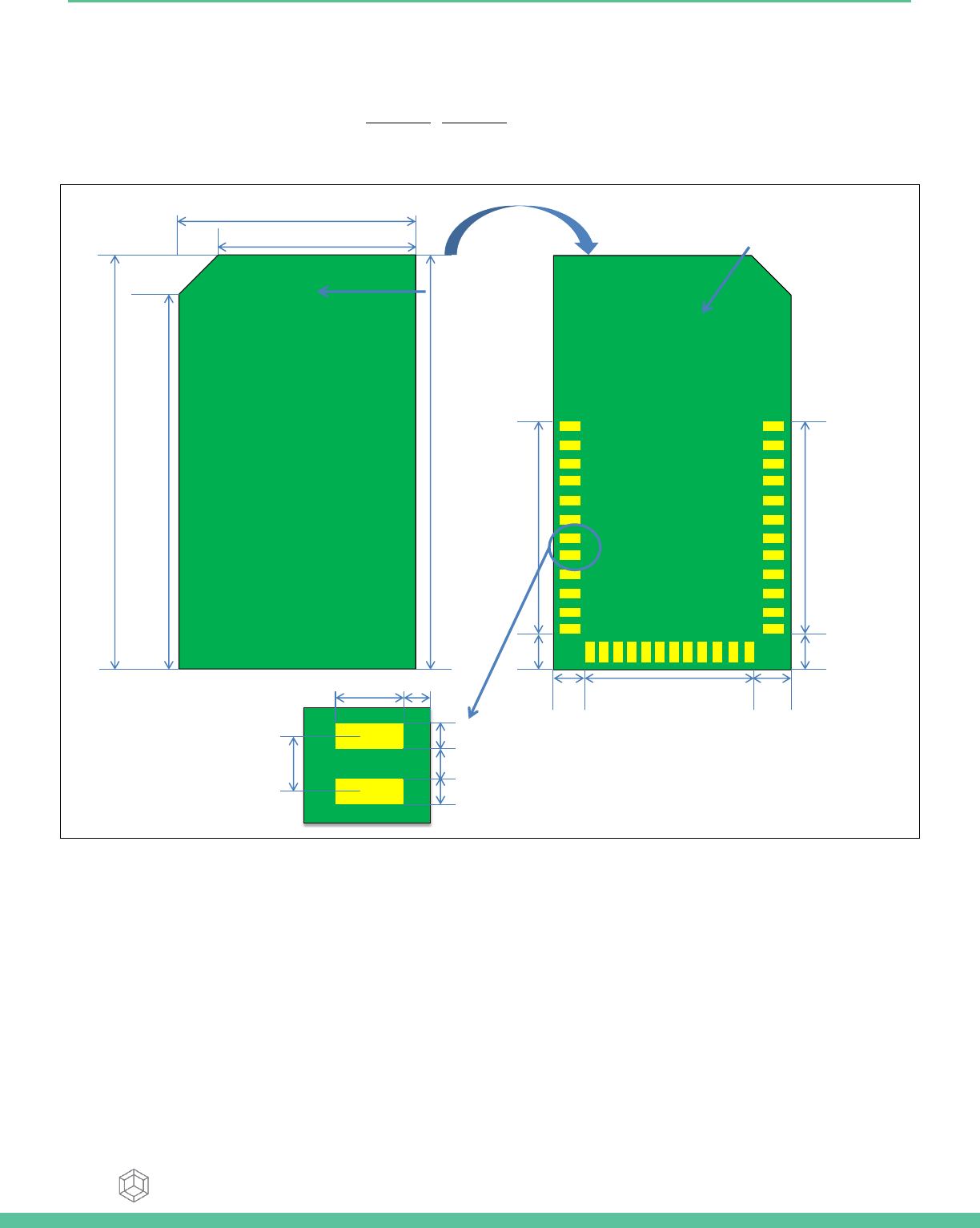
ARTIK 050 MODULE MECHANICAL SPECIFICATIONS
The ARTIK 050 Module supports 58x PADs. The mechanical dimensions of the top view and bottom view of the ARTIK 050
Module with its dimensions can be found in Figure 13. Figure 14 provides the part placement and part values of the most
important components on the ARTIK 050 Module.
Figure 13. ARTIK 050 Module Mechanical Drawing Views
18mm
North
West East
South
TOP
40mm
Wi-Fi antenna is
placed at the
north side.
Do not place any component on bottom
except defined solder plates.
1.5mm
North
East West
South
58
36
1
23
35 24
23 solder plates
27.0mm
12 solder plates
13.8mm
23 solder plates
27.0mm
BOTTOM
2.1mm 2.1mm
1.5mm
16mm
40mm
38mm
1.2mm
0.6mm
0.6mm
0.6mm
1.3mm 0.2mm
Samsung Semiconductor, Inc. ARTIK 050 Module Data Sheet
Samsung Confidential
Specifications in this document are tentative and subject to
change.
30
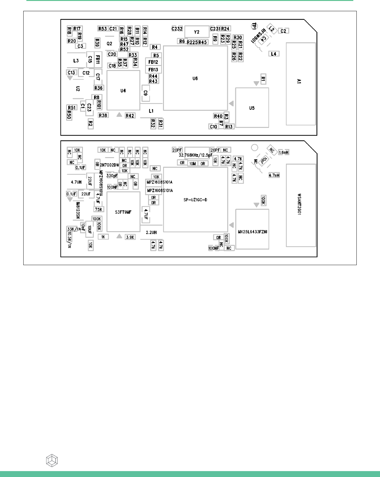
Figure 14. ARTIK 050 Module Part Placement and Part Values

Samsung Semiconductor, Inc. ARTIK 050 Module Data Sheet
Samsung Confidential
Specifications in this document are tentative and subject to
change.
32
FCC CERTIFICATION
This device complies with part 15 of the FCC Rules. Operation is subject to the following two conditions:
1. This device may not cause harmful interference, and
2. This device must accept any interference received, including interference that may cause undesired operation.
Caution: Any changes or modifications to the equipment not expressly approved by the party responsible for compliance
could void user’s authority to operate the equipment. This appliance and its antenna must not be co-located or operation in
conjunction with any other antenna or transmitter.
A minimum separation distance of 20cm must be maintained between the antenna and the person for this appliance to
satisfy the RF exposure requirements.
Instruction to OEM
This device complies with Industry Canada’s license-exempt RSSs. Operation is subject to the following two conditions:
1. This device may not cause interference and
2. This device must accept any interference, including interference that may cause
undesired operation of the device. This application and its antenna must not be co-located or operation in conjunction with
any other antenna or transmitter. A minimum separation distance of 20cm must be maintained between the antenna and
the person for this appliance to satisfy the RF exposure requirements. Host labeling requirement: “Contains transmitter
module
FCC ID: A3LATKM005000
IC ID: 649E-ATKM005000”
This device complies with part 15 of the FCC Rules. Operation is subject to the following two conditions:
1. This device may not cause harmful interference, and
2. This device must accept any interference received, including interference that may cause undesired operation.

Samsung Semiconductor, Inc. ARTIK 050 Module Data Sheet
Samsung Confidential
Specifications in this document are tentative and subject to
change.
33
LEGAL INFORMATION
INFORMATION IN THIS DOCUMENT IS PROVIDED IN CONNECTION WITH THE SAMSUNG ARTIK™ DEVELOPMENT KIT AND ALL
RELATED PRODUCTS, UPDATES, AND DOCUMENTATION (HEREINAFTER “SAMSUNG PRODUCTS”). NO LICENSE, EXPRESS OR
IMPLIED, BY ESTOPPEL OR OTHERWISE, TO ANY INTELLECTUAL PROPERTY RIGHTS IS GRANTED BY THIS DOCUMENT. THE
LICENSE AND OTHER TERMS AND CONDITIONS RELATED TO YOUR USE OF THE SAMSUNG PRODUCTS ARE GOVERNED
EXCLUSIVELY BY THE SAMSUNG ARTIK™ DEVELOPER LICENSE AGREEMENT THAT YOU AGREED TO WHEN YOU REGISTERED AS
A DEVELOPER TO RECEIVE THE SAMSUNG PRODUCTS. EXCEPT AS PROVIDED IN THE SAMSUNG ARTIK™ DEVELOPER LICENSE
AGREEMENT, SAMSUNG ELECTRONICS CO., LTD. AND ITS AFFILIATES (COLLECTIVELY, “SAMSUNG”) ASSUMES NO LIABILITY
WHATSOEVER, INCLUDING WITHOUT LIMITATION CONSEQUENTIAL OR INCIDENTAL DAMAGES, AND SAMSUNG DISCLAIMS
ANY EXPRESS OR IMPLIED WARRANTY, ARISING OUT OF OR RELATED TO YOUR SALE, APPLICATION AND/OR USE OF
SAMSUNG PRODUCTS INCLUDING LIABILITY OR WARRANTIES RELATED TO FITNESS FOR A PARTICULAR PURPOSE,
MERCHANTABILITY, OR INFRINGEMENT OF ANY PATENT, COPYRIGHT, OR OTHER INTELLECTUAL PROPERTY RIGHT.
SAMSUNG RESERVES THE RIGHT TO CHANGE PRODUCTS, INFORMATION, DOCUMENTATION AND SPECIFICATIONS WITHOUT
NOTICE. THIS INCLUDES MAKING CHANGES TO THIS DOCUMENTATION AT ANY TIME WITHOUT PRIOR NOTICE. THIS
DOCUMENTATION IS PROVIDED FOR REFERENCE PURPOSES ONLY, AND ALL INFORMATION DISCUSSED HEREIN IS PROVIDED
ON AN “AS IS” BASIS, WITHOUT WARRANTIES OF ANY KIND. SAMSUNG ASSUMES NO RESPONSIBILITY FOR POSSIBLE ERRORS
OR OMISSIONS, OR FOR ANY CONSEQUENCES FROM THE USE OF THE DOCUMENTATION CONTAINED HEREIN.
Samsung Products are not intended for use in medical, life support, critical care, safety equipment, or similar applications
where product failure could result in loss of life or personal or physical harm, or any military or defense application, or any
governmental procurement to which special terms or provisions may apply.
This document and all information discussed herein remain the sole and exclusive property of Samsung. All brand names,
trademarks and registered trademarks belong to their respective owners. For updates or additional information about
Samsung ARTIK™, contact the Samsung ARTIK™ team via the Samsung ARTIK™ website at www.artik.io.
Copyright © 2016 Samsung Electronics Co., Ltd.
All rights reserved. No part of this publication may be reproduced, stored in a retrieval system, or transmitted in any form or
by any means, electric or mechanical, by photocopying, recording, or otherwise, without the prior written consent of
Samsung Electronics.