Samsung Electronics Co RPMR500 Zigbee Module User Manual RP MR500 Manual final
Samsung Electronics Co Ltd Zigbee Module RP MR500 Manual final
manual

1
RP-MR500 Manual
1. INTRODUCTION
RP-MR500 is a full single-chip solution that is compliant to the specification of
IEEE802.15.4 and ZigBee specifications and is a complete wireless solution for
ZigBee applications such as home control and sensor network. It consists of RF
transceiver with baseband modem, a hardwired MAC and an embedded 8051
microcontroller with internal flash memory for application program. It also
includes several general-purpose I/O pins and many peripheral devices such as
timer and UART. The chip targets very low power and low voltage applications.
2. APPLICATIONS
- Home Automation and Security
- Automatic Meter Reading
- Factory Automation and Motor Control
- Replacement for legacy wired UART
- Energy Management
- Remote Keyless Entry with Acknowledgement
- Health-care equipments
- Pc peripherals and Toys

2
3. FEATURES
RF Transceiver
- Single-chip 2.4GHz ZigBee RF Transceiver module
- Low Power Consumption
- Low Operation Voltage of 1.9V
- high Sensitivity (-98dBm)
- On-chip VCO, LNA, and PA
- Programmable Output Power Max. +6dBm
- O-QPSK Modulation
- Scalable Data Rate: 250Kbps/500K/1M
- RSSI Measurement
- Compliant to IEEE802.15.4
8051-Compatible Microcontroller
- 8051 Compatible Microcontroller
- 96KB Embedded Flash Memory
- 8KB Data Memory
- 128-byte CPU dedicated Memory
- 1KB Boot ROM
- 24 General Purpose I/Os
- On-chip Power-on-Reset
- 4-channel 12-bit ADC
- ISP (In System Programming)
- Internal Temperature Sensor
Clock Inputs & Power
- 16MHz Crystal for System Clock
- Separate On-chip Regulators for Analog and Digital Circuitry
- Power Supply Range for Internal Regulator
- Battery Monitoring Support

3
4. SPECIFICATION
1) Description
Item
Description
Application
Transceiver Mod ule
Frequency Range 2.425 ~ 2.475 GHz (ISM Band)
I/O Supply Voltage 1.9~3.6V (Recommend)
Current 50 mA
Operating Temperature -40 ~
85℃
Standard Spec.
IEEE802.15.4
Type
SMD
Type
Size
24 x 41 x 4
mm
2) Electrical specifications
Parameter
Min Typ Max Unit
RF Frequency Range 2425 2475 MHz
RF Bandwidth
2
MHz
Channel Bandwidth
5
MHz
RF Output Power
2
5
8
dBm
Receiver Sensitivity
(PER≤1%, Packet length of 22-byte)
Normal mode (250 kbps)
-98
dBm
Maximum Input Level
10
dBm
Current : RF Receive Mode
35
mA
Current : RF Transmit Mode
45
mA
Current : Sleep Mode
25
90
uA

4
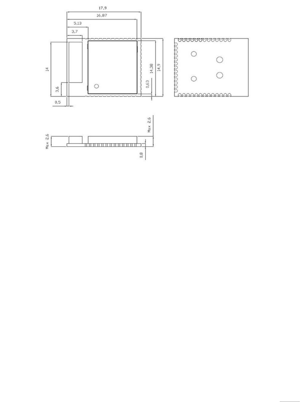
5. Module Dimension

5
6. PIN Description
Terminal
NAME
Interface
I/O
Description
1
ACH0
Analog
I/O
Sensor ADC input
2
ACH1
Analog
I/O
Sensor ADC input
3
ACH2
Analog
I/O
Sensor ADC input
4
ACH3
Analog
I/O
Sensor ADC input
5
AVDD_1.5V Power
I/O
1.5V Power Supply input/output
6
AGND Ground
-
RF Ground
7
MS0
Digital
I
Mode select
8
MS1
Digital
I
Mode select
9
MS2
Digital
I
Mode select
10
MSV
Digital
I
Mode select of voltage(0=1.5V)
11
RESETB Digital
I
Reset (Active Low)
12
3V_IN
Power
I
3V Power supply
13
DGND Ground
-
Ground for digital core and I/O
14
P1[7]
Digital
O
Port P1.7GPO/P0AND/TRSW
15
P1[6]
Digital
B
Port P1.6/TRSWB
16
P1[5]
Digital
B
Port P1.5
17
P1[4]
Digital
B
Port P1.4 /QUADZB/Sleep Timer OSC Buffer Input.
18
P1[3]
Digital
B
Port P1.3/QUADZA/Sleep Timer OSC Buffer Output/RTCLKOUT
19
P1[2]
Digital
B
Port P1.2
20
P1[1]
Digital
B
Port P1.1/TXD1
21
P1[0]
Digital
B
Port P1.0/RXD1
22
P3[7]
Digital
B
Port P3.7/12mA Drive capability
/PWM3/CTS1/SPICSN(slave
only)
23
P3[6]
Digital
B
Port P3.6/12 mA Drive capability /PWM2/RTS1/SPICLK

6
Terminal
NAME
Interface I/O
Des
c
ription
24
P3[5]
Digital
B
Port P3.5/T1/CTS0/QUADYB/SPIDO
25
P3[4]
Digital
B
Port P3.4/T0/RTS0/QUADYA/SPIDI
26
P3[3]
Digital
B
Port P3.3/INT1(active low)
27
P3[2]
Digital
B
Port P3.2/INT0(active low)
28
P3[1]
Digital
B
Port P3.1/TXD0/QUADXB
29
P3[0]
Digital
B
Port P3.0/RXD0/QUADXA
30
DGND
Ground
-
Ground for digital core and I/O
31
DVDD_1.5V Power
I/O
1.5V Power Supply input/output
32
P0[7]
Digital
B
Port P0.7/I2STX_MCLK
33
P0[6]
Digital
B
Port P0.6/I2STX_BCLK
34
P0[5]
Digital
B
Port P0.5/I2STX_LRCK
35
P0[4]
Digital
B
Port P0.4/I2STX_DO
36
P0[3]
Digital
B
Port P0.3/I2SRX_MCLK
37
P0[2]
Digital
B
Port P0.2/I2SRX_BCLK
38
P0[1]
Digital
B
Port P0.1/I2SRX_LRCK
39
P0[0]
Digital
B
Port P0.0/I2SRX_DI
40
NC
NC
-
No Connection
41
NC
NC
-
No Connection
42
AGND
Ground
-
RF Ground
43
DGND
Ground
-
Ground for digital core and I/O
44
DGND
Ground
-
Ground for digital core and I/O
45
AGND
Ground
-
RF Ground
7. Contact Information
RadioPulse Inc.
3rd fl., Hans II bldg., 111-6 Seongnae-dong, Gangdong-gu, Seoul, 134-883, Korea
Tel : +82 2 478 2963~5
Fax : +82 2 478 2966~7

7
FCC Statement
Federal Communication Commission Interference Statement
This equipment has been tested and found to comply with the limits for a Class B digital device,
pursuant to Part 15 of the FCC Rules. These limits are designed to provide reasonable protection
against harmful interference in a residential installation. This equipment generates, uses and can
radiate radio frequency energy and, if not installed and used in accordance with the instructions,
may cause harmful interference to radio communications. However, there is no guarantee that
interference will not occur in a particular installation. If this equipment does cause harmful
interference to radio or television reception, which can be determined by turning the equipment
off and on, the user is encouraged to try to correct the interference by one of the following
measures:
Reorient or relocate the receiving antenna.
Increase the separation between the equipment and receiver.
Connect the equipment into an outlet on a circuit different from that to which the receiver is
connected.
Consult the dealer or an experienced radio/TV technician for help.
FCC Caution:
Any changes or modifications not expressly approved by the party responsible for compliance
could void the user’s authority to operate this equipment.
This device complies with Part 15 of the FCC Rules. Operation is subject to the following two
conditions:
(1) This device may not cause harmful interference, and
(2) this device must accept any interference received, including interference that may cause
undesired operation.
This device and its antenna(s) must not be co-located or operation in conjunction with any other
antenna or transmitter.
IMPORTANT NOTE:
FCC Radiation Exposure Statement:
This equipment complies with FCC radiation exposure limits set forth for an uncontrolled
environment.
IMPORTANT NOTE:
This module is intended for OEM integrator. The OEM integrator is still responsible for the FCC

8
compliance requirement of the end product, which integrates this module.
Any changes or modifications not expressly approved by the manufacturer could void the user's
authority to operate this equipment.
USERS MANUAL OF THE END PRODUCT:
The end user has to be informed that any changes or modifications not expressly approved by
the manufacturer could void the user's authority to operate this equipment. If the size of the end
product is smaller than 8x10cm, then additional FCC part 15.19 statement is required to be
available in the users manual: This device complies with Part 15 of FCC rules. Operation is
subject to the following two conditions: (1) this device may not cause harmful interference and (2)
this device must accept any interference received, including interference that may cause undesired
operation.
LABEL OF THE END PRODUCT:
The final end product must be labeled in a visible area with the following " Contains TX FCC
ID:A3LRPMR500
". If the size of the end product is larger than 8x10cm, then the following FCC
part 15.19 statement has to also be available on the label: This device complies with Part 15 of FCC
rules. Operation is subject to the following two conditions: (1) this device may not cause harmful
interference and (2) this device must accept any interference received, including interference that may
cause undesired operation.