Sierra Wireless HL7650 HL7650 module User Manual
Sierra Wireless Inc. HL7650 module
UserManual.wiki
>
Sierra Wireless
>
HL7650 User Manual
User manual
Navigation menu
Upload a User Manual
Namespaces
Wiki Guide
HTML
PDF
Info
Views
User Manual
Discussion / Help
Navigation
![41110363 Rev 4.0 October 18, 2017 16 Product Technical Specification Introduction 1.8.2. Regulatory Sierra Wireless hereby declares that the HL7650 is in compliance with all essential requirements of Directive <TBD>. The Declaration of Conformity will be available for viewing at the following location in the EU community: Sierra Wireless (UK) Limited Suite 5, The Hub Fowler Avenue Farnborough Business Park Farnborough, United Kingdom GU14 7JP 1.8.3. RoHS Directive Compliant The AirPrime HL7650 module is compliant with RoHS Directive 2011/65/EU which sets limits for the use of certain restricted hazardous substances. This directive states that “from 1st July 2006, new electrical and electronic equipment put on the market does not contain lead, mercury, cadmium, hexavalent chromium, polybrominated biphenyls (PBB) or polybrominated diphenyl ethers (PBDE)”. 1.8.4. Disposing of the Product This electronic product is subject to the EU Directive 2012/19/EU for Waste Electrical and Electronic Equipment (WEEE). As such, this product must not be disposed of at a municipal waste collection point. Please refer to local regulations for directions on how to dispose of this product in an environmental friendly manner. 1.9. References [1] AirPrime HL Series Customer Process Guidelines Reference Number: 4114330 [2] AirPrime HL76xx AT Commands Interface Guide Reference Number: 4118395 [3] AirPrime HL Series Development Kit User Guide Reference Number: 4114877](https://usermanual.wiki/Sierra-Wireless/HL7650/User-Guide-3636355-Page-16.png)
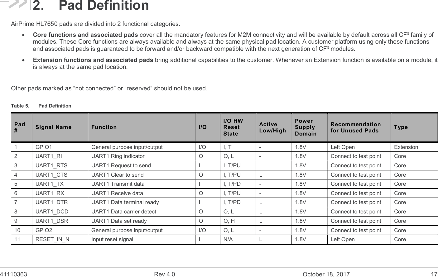
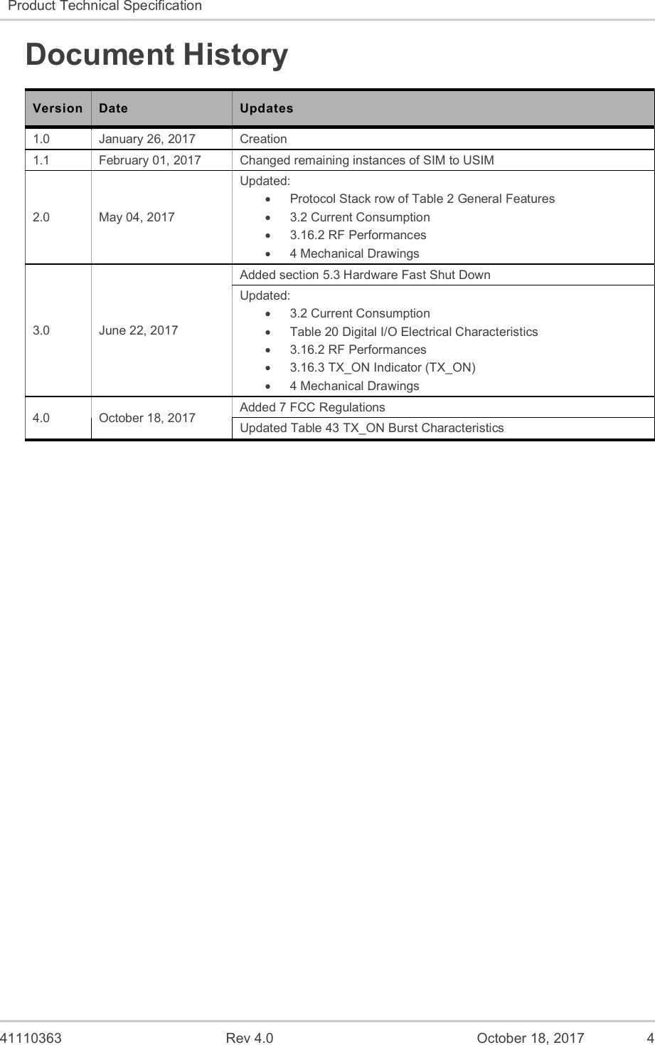
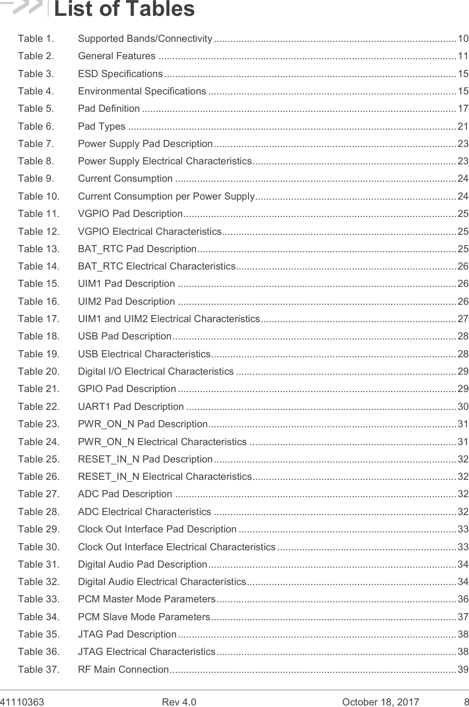
![41110363 Rev 4.0 October 18, 2017 28 Product Technical Specification Detailed Interface Specifications Enabling or disabling this UIM detect feature can be done using the AT+KSIMDET command. For more information about this command, refer to document [2] AirPrime HL76xx AT Commands Interface Guide. 3.6. USB Interface The AirPrime HL7650 has one Universal Serial Bus interface complaint with USB Rev 2.0. Refer to the following table for the pad description of the USB interface. Table 18. USB Pad Description Pad Number Signal Name I/O Function 12 USB_D- I/O USB Data Negative 13 USB_D+ I/O USB Data Positive 16 USB_VBUS I USB VBUS Note: When the 5V USB supply is not available, connect USB_VBUS to VBATT to supply the USB interface. Refer to the following table for the electrical characteristics of the USB interface. Table 19. USB Electrical Characteristics Parameter Minimum Typical Maximum Units Test Condition Input voltage at pads USB_D+ / USB_D- -0.3 - 3.6 V Voltage USB_VBUS 0 - 5.25 V Full Speed Mode Signal Rate 11.994 - 12.006 Mbit/s EOP (end of packet) Width 160 - 175 ns Rising Edge 4 - 20 ns At 10% and 90% Falling Edge 4 - 20 ns At 10% and 90% High Speed Mode Signal Rate 479.760 - 480.024 Mbit/s EOP (end of packet) Width 15.625 - 17.7073 ns Rising Edge 500 - ps At 10% and 90% Falling Edge 500 - ps At 10% and 90%](https://usermanual.wiki/Sierra-Wireless/HL7650/User-Guide-3636355-Page-28.png)
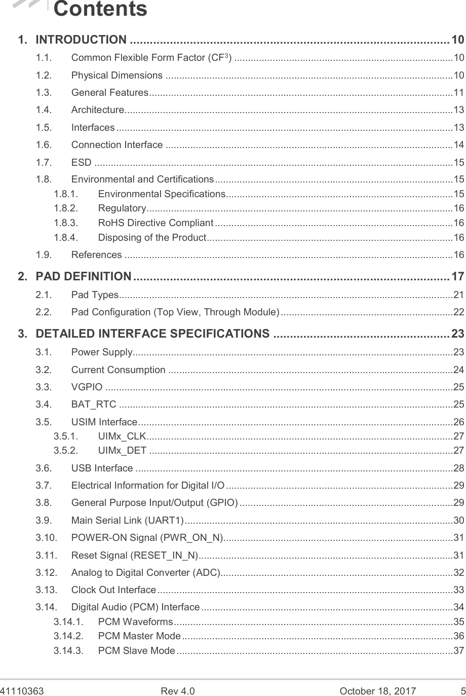
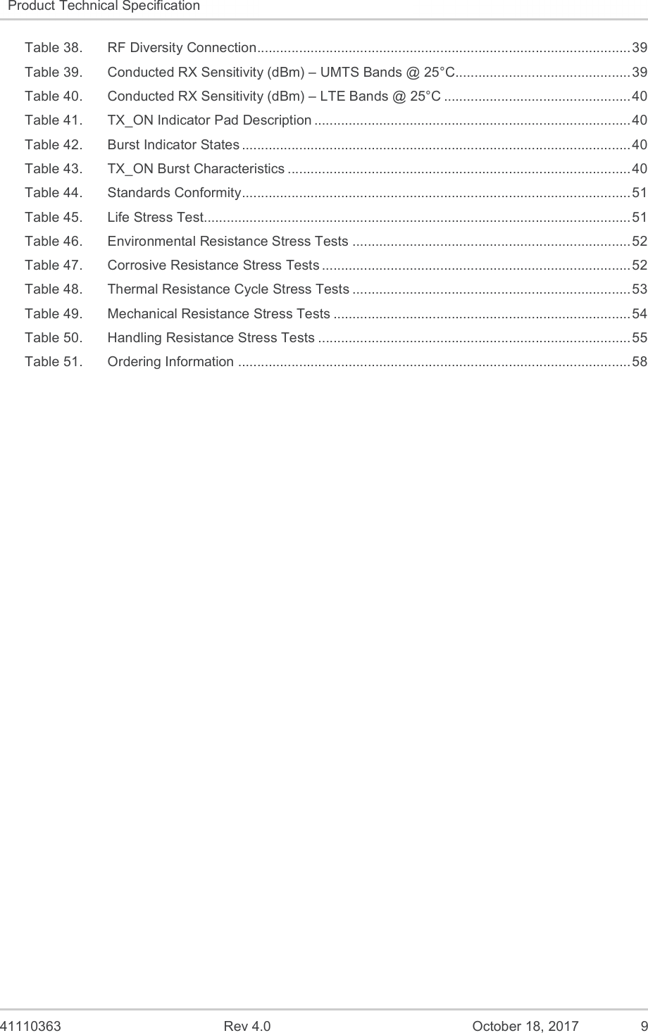
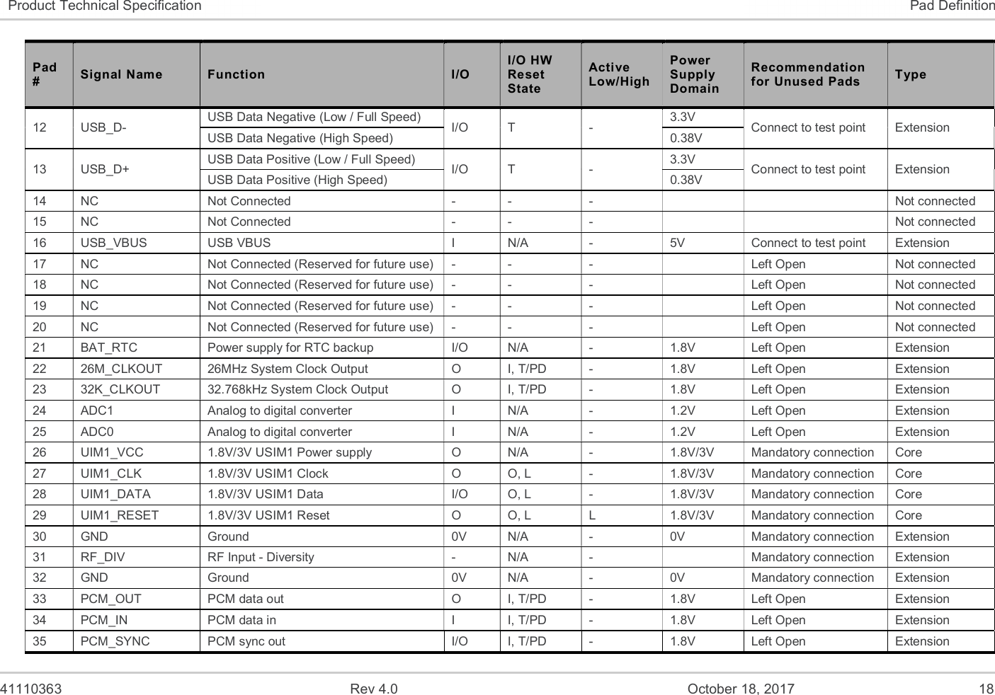
![41110363 Rev 4.0 October 18, 2017 33 Product Technical Specification Detailed Interface Specifications Parameter Minimum Typical Maximum Remarks Current tolerance - - ± 3% Quiescent current (µA) - 710 - Wake-up time from power save (µs) - 50 - 3.13. Clock Out Interface The AirPrime HL7650 module supports two digital clock out interfaces. Enabling or disabling the clock out feature can be done using AT commands. For more information about AT commands, refer to document [2] AirPrime HL76xx AT Commands Interface Guide. Refer to the following table for the pad description of the clock out interface. Table 29. Clock Out Interface Pad Description Pad Number Signal Name I/O I/O Type Description 22 26M_CLKOUT O 1.8V 26MHz Digital Clock output 23 32K_CLKOUT O 1.8V 32.768kHz Digital Clock output Refer to the following table for the electrical characteristics of the clock out interface. Table 30. Clock Out Interface Electrical Characteristics Parameter Symbol Minimum Typical Maximum Units CLKOUTn period at 26MHz (tr1) - 38 - ns CLKOUTn low time at 26MHz (tr2) 10 - - ns CLKOUTn high time at 26MHz (tr3) 10 - - ns CLKOUTn period at 32.768KHz (tr1) - - - ns CLKOUTn low time at 32.768KHz (tr2) - - - ns CLKOUTn high time at 32.768KHz (tr3) - - - ns Period jitter - - 4 ns The following figure shows the clock out (CLKOUT) timing waveform. Figure 7. CLKOUTx Timing Waveform](https://usermanual.wiki/Sierra-Wireless/HL7650/User-Guide-3636355-Page-33.png)
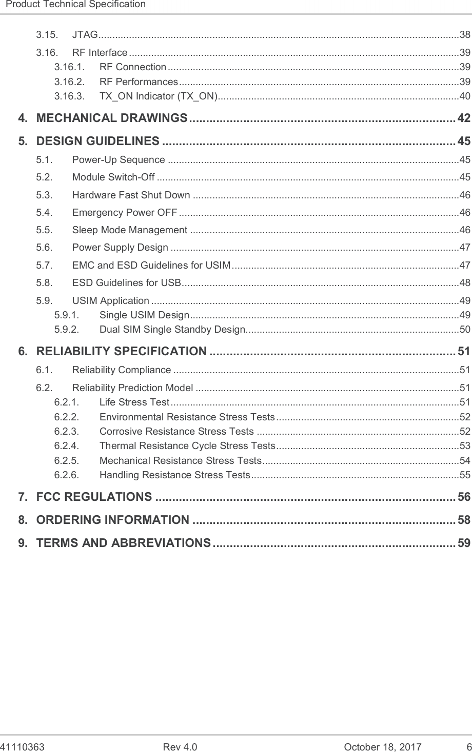
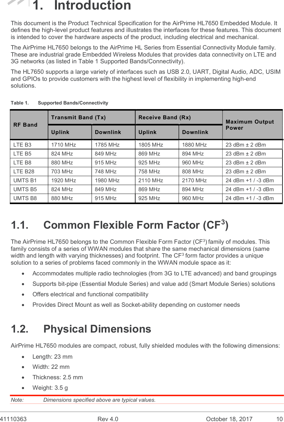
![41110363 Rev 4.0 October 18, 2017 39 Product Technical Specification Detailed Interface Specifications 3.16. RF Interface The RF interface of the AirPrime HL7650 module allows the transmission of RF signals. This interface has a 50Ω nominal impedance. Note that if the final application is a single antenna receiver (does not use the diversity antenna), it is recommended that the diversity antenna be disabled using AT command AT+WMANTSEL. Disabling the diversity antenna when not used: prevents any noise in the diversity antenna input from degrading the overall sensitivity performance of the main RF input, and reduces the power consumption of the module. Refer to document [2] AirPrime HL76xx AT Commands Interface Guide for more information regarding AT+WMANTSEL. 3.16.1. RF Connection A 50Ω (with maximum VSWR 1.1:1, and 0.5 dB loss) RF track is recommended to be connected to standard RF connectors such as SMA, UFL, etc. for antenna connection. Refer to the following tables for the pad description of the RF interface. Table 37. RF Main Connection Pad Number RF Signal Impedance VSWR Rx (max) VSWR Tx (max) 49 RF_MAIN 50Ω 1.5:1 1.5:1 Table 38. RF Diversity Connection Pad Number RF Signal Impedance VSWR Rx (max) VSWR Tx (max) 31 RF_DIV 50Ω 1.5:1 --- 3.16.2. RF Performances Table 39. Conducted RX Sensitivity (dBm) – UMTS Bands @ 25°C Frequency Band Primary (Typical) Secondary (Typical) UMTS B1 0.1% BER 12.2 kbps -108 -111 UMTS B5 -111 -112 UMTS B8 -110 -111.5 4G RF performances are compliant with 3GPP recommendation TS 36.101.](https://usermanual.wiki/Sierra-Wireless/HL7650/User-Guide-3636355-Page-39.png)
![41110363 Rev 4.0 October 18, 2017 54 Product Technical Specification Reliability Specification 6.2.5. Mechanical Resistance Stress Tests The following tests the AirPrime HL7650 module’s resistance to vibrations and mechanical shocks. Table 49. Mechanical Resistance Stress Tests Designation Condition Sinusoidal Vibration Test SVT Standard: IEC 60068-2-6, Test Fc Special conditions: Frequency range: 16 Hz to 1000 Hz Displacement: 0.35mm (peak-peak) Acceleration: 5G from 16 to 62 Hz 3G from 62 to 200 Hz 1G from 200 to 1000 Hz Sweep rate: 1 octave / cycle Number of Sweep: 20 sweeps/axis Sweep direction: ± X, ± Y, ± Z Operating conditions: Un-powered Duration: 2 days Random Vibration Test RVT Standard: IEC 60068-2-64, Test Fh Special conditions: Frequency range: 10 Hz – 2000 Hz Power Spectral Density in [(m/s²)²/Hz] 0.1 g2/Hz at 10Hz 0.01 g2/Hz at 250Hz 0.005 g2/Hz at 1000Hz 0.005 g2/Hz at 2000Hz Peak factor: 3 Duration per Axis: 1 hr / axis Operating conditions: Un-powered Duration: 1 day Mechanical Shock Test MST Standard: IEC 60068-2-27, Test Ea Special conditions: Shock Test 1: Wave form: Half sine Peak acceleration: 30g Duration: 11ms Number of shocks: 8 Direction: ±X, ±Y, ±Z Shock Test 2: Wave form: Half sine Peak acceleration: 100g Duration: 6ms Number of shocks: 3 Direction: ±X, ±Y, ±Z Operating conditions: Un-powered Duration: 72 hours](https://usermanual.wiki/Sierra-Wireless/HL7650/User-Guide-3636355-Page-54.png)