Sierra Wireless HL7650 HL7650 module User Manual
Sierra Wireless Inc. HL7650 module
User manual

Product Technical Specification
AirPrime HL7650
41110363
4.0
October 18, 2017

41110363 Rev 4.0 October 18, 2017 2
Product Technical Specification
Important Notice
Due to the nature of wireless communications, transmission and reception of data can never be
guaranteed. Data may be delayed, corrupted (i.e., have errors) or be totally lost. Although significant
delays or losses of data are rare when wireless devices such as the Sierra Wireless modem are used
in a normal manner with a well-constructed network, the Sierra Wireless modem should not be used
in situations where failure to transmit or receive data could result in damage of any kind to the user or
any other party, including but not limited to personal injury, death, or loss of property. Sierra Wireless
accepts no responsibility for damages of any kind resulting from delays or errors in data transmitted or
received using the Sierra Wireless modem, or for failure of the Sierra Wireless modem to transmit or
receive such data.
Safety and Hazards
Do not operate the Sierra Wireless modem in areas where cellular modems are not advised without
proper device certifications. These areas include environments where cellular radio can interfere such
as explosive atmospheres, medical equipment, or any other equipment which may be susceptible to
any form of radio interference. The Sierra Wireless modem can transmit signals that could interfere
with this equipment. Do not operate the Sierra Wireless modem in any aircraft, whether the aircraft is
on the ground or in flight. In aircraft, the Sierra Wireless modem MUST BE POWERED OFF. When
operating, the Sierra Wireless modem can transmit signals that could interfere with various onboard
systems.
Note: Some airlines may permit the use of cellular phones while the aircraft is on the ground and the door
is open. Sierra Wireless modems may be used at this time.
The driver or operator of any vehicle should not operate the Sierra Wireless modem while in control of
a vehicle. Doing so will detract from the driver or operator’s control and operation of that vehicle. In
some states and provinces, operating such communications devices while in control of a vehicle is an
offence.
Limitations of Liability
This manual is provided “as is”. Sierra Wireless makes no warranties of any kind, either expressed or
implied, including any implied warranties of merchantability, fitness for a particular purpose, or
noninfringement. The recipient of the manual shall endorse all risks arising from its use.
The information in this manual is subject to change without notice and does not represent a
commitment on the part of Sierra Wireless. SIERRA WIRELESS AND ITS AFFILIATES
SPECIFICALLY DISCLAIM LIABILITY FOR ANY AND ALL DIRECT, INDIRECT, SPECIAL,
GENERAL, INCIDENTAL, CONSEQUENTIAL, PUNITIVE OR EXEMPLARY DAMAGES INCLUDING,
BUT NOT LIMITED TO, LOSS OF PROFITS OR REVENUE OR ANTICIPATED PROFITS OR
REVENUE ARISING OUT OF THE USE OR INABILITY TO USE ANY SIERRA WIRELESS
PRODUCT, EVEN IF SIERRA WIRELESS AND/OR ITS AFFILIATES HAS BEEN ADVISED OF THE
POSSIBILITY OF SUCH DAMAGES OR THEY ARE FORESEEABLE OR FOR CLAIMS BY ANY
THIRD PARTY.
Notwithstanding the foregoing, in no event shall Sierra Wireless and/or its affiliates aggregate liability
arising under or in connection with the Sierra Wireless product, regardless of the number of events,
occurrences, or claims giving rise to liability, be in excess of the price paid by the purchaser for the
Sierra Wireless product.

41110363 Rev 4.0 October 18, 2017 3
Product Technical Specification
Patents
This product may contain technology developed by or for Sierra Wireless Inc.
This product includes technology licensed from QUALCOMM
®
.
This product is manufactured or sold by Sierra Wireless Inc. or its affiliates under one or more patents
licensed from MMP Portfolio Licensing.
Copyright
© 2017 Sierra Wireless. All rights reserved.
Trademarks
Sierra Wireless
®
, AirPrime
®
, AirLink
®
, AirVantage
®
, WISMO
®
, ALEOS
®
and the Sierra Wireless and
Open AT logos are registered trademarks of Sierra Wireless, Inc. or one of its subsidiaries.
Watcher
®
is a registered trademark of NETGEAR, Inc., used under license.
Windows
®
and Windows Vista
®
are registered trademarks of Microsoft Corporation.
Macintosh
®
and Mac OS X
®
are registered trademarks of Apple Inc., registered in the U.S. and other
countries.
QUALCOMM
®
is a registered trademark of QUALCOMM Incorporated. Used under license.
Other trademarks are the property of their respective owners.
Contact Information
Sales information and technical support,
including warranty and returns
Web: sierrawireless.com/company/contact-us/
Global toll-free number: 1-877-687-7795
6:00 am to 5:00 pm PST
Corporate and product information Web: sierrawireless.com
41110363 Rev 4.0 October 18, 2017 4
Product Technical Specification
Document History
Version
Date Updates
1.0 January 26, 2017 Creation
1.1 February 01, 2017 Changed remaining instances of SIM to USIM
2.0 May 04, 2017
Updated:
Protocol Stack row of Table 2 General Features
3.2 Current Consumption
3.16.2 RF Performances
4 Mechanical Drawings
3.0 June 22, 2017
Added section 5.3 Hardware Fast Shut Down
Updated:
3.2 Current Consumption
Table 20 Digital I/O Electrical Characteristics
3.16.2 RF Performances
3.16.3 TX_ON Indicator (TX_ON)
4 Mechanical Drawings
4.0 October 18, 2017 Added 7 FCC Regulations
Updated Table 43 TX_ON Burst Characteristics

41110363 Rev 4.0 October 18, 2017 5
Contents
1. INTRODUCTION ................................................................................................ 10
1.1. Common Flexible Form Factor (CF3) ................................................................................ 10
1.2. Physical Dimensions ......................................................................................................... 10
1.3. General Features ............................................................................................................... 11
1.4. Architecture........................................................................................................................ 13
1.5. Interfaces ........................................................................................................................... 13
1.6. Connection Interface ......................................................................................................... 14
1.7. ESD ................................................................................................................................... 15
1.8. Environmental and Certifications ....................................................................................... 15
1.8.1. Environmental Specifications ................................................................................... 15
1.8.2. Regulatory ................................................................................................................ 16
1.8.3. RoHS Directive Compliant ....................................................................................... 16
1.8.4. Disposing of the Product .......................................................................................... 16
1.9. References ........................................................................................................................ 16
2. PAD DEFINITION ............................................................................................... 17
2.1. Pad Types .......................................................................................................................... 21
2.2. Pad Configuration (Top View, Through Module) ............................................................... 22
3. DETAILED INTERFACE SPECIFICATIONS ..................................................... 23
3.1. Power Supply..................................................................................................................... 23
3.2. Current Consumption ........................................................................................................ 24
3.3. VGPIO ............................................................................................................................... 25
3.4. BAT_RTC .......................................................................................................................... 25
3.5. USIM Interface ................................................................................................................... 26
3.5.1. UIMx_CLK ................................................................................................................ 27
3.5.2. UIMx_DET ............................................................................................................... 27
3.6. USB Interface .................................................................................................................... 28
3.7. Electrical Information for Digital I/O ................................................................................... 29
3.8. General Purpose Input/Output (GPIO) .............................................................................. 29
3.9. Main Serial Link (UART1) .................................................................................................. 30
3.10. POWER-ON Signal (PWR_ON_N).................................................................................... 31
3.11. Reset Signal (RESET_IN_N) ............................................................................................. 31
3.12. Analog to Digital Converter (ADC)..................................................................................... 32
3.13. Clock Out Interface ............................................................................................................ 33
3.14. Digital Audio (PCM) Interface ............................................................................................ 34
3.14.1. PCM Waveforms ...................................................................................................... 35
3.14.2. PCM Master Mode ................................................................................................... 36
3.14.3. PCM Slave Mode ..................................................................................................... 37

41110363 Rev 4.0 October 18, 2017 6
Product Technical Specification
3.15. JTAG .................................................................................................................................. 38
3.16. RF Interface ....................................................................................................................... 39
3.16.1. RF Connection ......................................................................................................... 39
3.16.2. RF Performances ..................................................................................................... 39
3.16.3. TX_ON Indicator (TX_ON) ....................................................................................... 40
4.
MECHANICAL DRAWINGS ............................................................................... 42
5.
DESIGN GUIDELINES ....................................................................................... 45
5.1. Power-Up Sequence ......................................................................................................... 45
5.2. Module Switch-Off ............................................................................................................. 45
5.3. Hardware Fast Shut Down ................................................................................................ 46
5.4. Emergency Power OFF ..................................................................................................... 46
5.5. Sleep Mode Management ................................................................................................. 46
5.6. Power Supply Design ........................................................................................................ 47
5.7. EMC and ESD Guidelines for USIM .................................................................................. 47
5.8. ESD Guidelines for USB .................................................................................................... 48
5.9. USIM Application ............................................................................................................... 49
5.9.1. Single USIM Design ................................................................................................. 49
5.9.2. Dual SIM Single Standby Design............................................................................. 50
6.
RELIABILITY SPECIFICATION ......................................................................... 51
6.1. Reliability Compliance ....................................................................................................... 51
6.2. Reliability Prediction Model ............................................................................................... 51
6.2.1. Life Stress Test ........................................................................................................ 51
6.2.2. Environmental Resistance Stress Tests .................................................................. 52
6.2.3. Corrosive Resistance Stress Tests ......................................................................... 52
6.2.4. Thermal Resistance Cycle Stress Tests .................................................................. 53
6.2.5. Mechanical Resistance Stress Tests ....................................................................... 54
6.2.6. Handling Resistance Stress Tests ........................................................................... 55
7.
FCC REGULATIONS ......................................................................................... 56
8.
ORDERING INFORMATION .............................................................................. 58
9.
TERMS AND ABBREVIATIONS ........................................................................ 59

41110363 Rev 4.0 October 18, 2017 7
List of Figures
Figure 1. Architecture Overview ..................................................................................................... 13
Figure 2. Mechanical Overview (Top and Bottom Views) .............................................................. 14
Figure 3. AirPrime HL7650 Top View ............................................................................................. 14
Figure 4. AirPrime HL7650 Bottom View ........................................................................................ 14
Figure 5. Pad Configuration ............................................................................................................ 22
Figure 6. UIMx Timing Waveform ................................................................................................... 27
Figure 7. CLKOUTx Timing Waveform ........................................................................................... 33
Figure 8. PCM Timing Waveform ................................................................................................... 35
Figure 9. PCM Master Mode Timing ............................................................................................... 36
Figure 10. PCM Master Mode Timing ............................................................................................... 37
Figure 11. JTAG Timing Waveform .................................................................................................. 38
Figure 12. TX_ON State During Transmission ................................................................................. 41
Figure 13. Mechanical Drawing ........................................................................................................ 42
Figure 14. Dimensions Drawing ....................................................................................................... 43
Figure 15. Footprint .......................................................................................................................... 44
Figure 16. PWR_ON_N Sequence with VGPIO Information ............................................................ 45
Figure 17. Power OFF Sequence for PWR_ON_N, VGPIO ............................................................. 45
Figure 18. Fast Shutdown Power OFF Sequence ............................................................................ 46
Figure 19. Voltage Limiter Example ................................................................................................. 47
Figure 20. EMC and ESD Components Close to the USIM ............................................................. 48
Figure 21. ESD Protection for USB .................................................................................................. 48
Figure 22. Single USIM Application (1 USIM Slot and 1 USIM Connector) ..................................... 49
Figure 23. Dual SIM Single Standby Application (1 USIM Slot and 2 USIM Connectors) ............... 50

41110363 Rev 4.0 October 18, 2017 8
List of Tables
Table 1. Supported Bands/Connectivity ........................................................................................ 10
Table 2. General Features ............................................................................................................ 11
Table 3. ESD Specifications .......................................................................................................... 15
Table 4. Environmental Specifications .......................................................................................... 15
Table 5. Pad Definition .................................................................................................................. 17
Table 6. Pad Types ....................................................................................................................... 21
Table 7. Power Supply Pad Description ........................................................................................ 23
Table 8. Power Supply Electrical Characteristics .......................................................................... 23
Table 9. Current Consumption ...................................................................................................... 24
Table 10. Current Consumption per Power Supply ......................................................................... 24
Table 11. VGPIO Pad Description ................................................................................................... 25
Table 12. VGPIO Electrical Characteristics ..................................................................................... 25
Table 13. BAT_RTC Pad Description .............................................................................................. 25
Table 14. BAT_RTC Electrical Characteristics................................................................................ 26
Table 15. UIM1 Pad Description ..................................................................................................... 26
Table 16. UIM2 Pad Description ..................................................................................................... 26
Table 17. UIM1 and UIM2 Electrical Characteristics ....................................................................... 27
Table 18. USB Pad Description ....................................................................................................... 28
Table 19. USB Electrical Characteristics ......................................................................................... 28
Table 20. Digital I/O Electrical Characteristics ................................................................................ 29
Table 21. GPIO Pad Description ..................................................................................................... 29
Table 22. UART1 Pad Description .................................................................................................. 30
Table 23. PWR_ON_N Pad Description .......................................................................................... 31
Table 24. PWR_ON_N Electrical Characteristics ........................................................................... 31
Table 25. RESET_IN_N Pad Description ........................................................................................ 32
Table 26. RESET_IN_N Electrical Characteristics .......................................................................... 32
Table 27. ADC Pad Description ...................................................................................................... 32
Table 28. ADC Electrical Characteristics ........................................................................................ 32
Table 29. Clock Out Interface Pad Description ............................................................................... 33
Table 30. Clock Out Interface Electrical Characteristics ................................................................. 33
Table 31. Digital Audio Pad Description .......................................................................................... 34
Table 32. Digital Audio Electrical Characteristics ............................................................................ 34
Table 33. PCM Master Mode Parameters ....................................................................................... 36
Table 34. PCM Slave Mode Parameters ......................................................................................... 37
Table 35. JTAG Pad Description ..................................................................................................... 38
Table 36. JTAG Electrical Characteristics ....................................................................................... 38
Table 37. RF Main Connection ........................................................................................................ 39

41110363 Rev 4.0 October 18, 2017 9
Product Technical Specification
Table 38. RF Diversity Connection .................................................................................................. 39
Table 39. Conducted RX Sensitivity (dBm) – UMTS Bands @ 25°C .............................................. 39
Table 40. Conducted RX Sensitivity (dBm) – LTE Bands @ 25°C ................................................. 40
Table 41. TX_ON Indicator Pad Description ................................................................................... 40
Table 42. Burst Indicator States ...................................................................................................... 40
Table 43. TX_ON Burst Characteristics .......................................................................................... 40
Table 44. Standards Conformity ...................................................................................................... 51
Table 45. Life Stress Test................................................................................................................ 51
Table 46. Environmental Resistance Stress Tests ......................................................................... 52
Table 47. Corrosive Resistance Stress Tests ................................................................................. 52
Table 48. Thermal Resistance Cycle Stress Tests ......................................................................... 53
Table 49. Mechanical Resistance Stress Tests .............................................................................. 54
Table 50. Handling Resistance Stress Tests .................................................................................. 55
Table 51. Ordering Information ....................................................................................................... 58
41110363 Rev 4.0 October 18, 2017 10
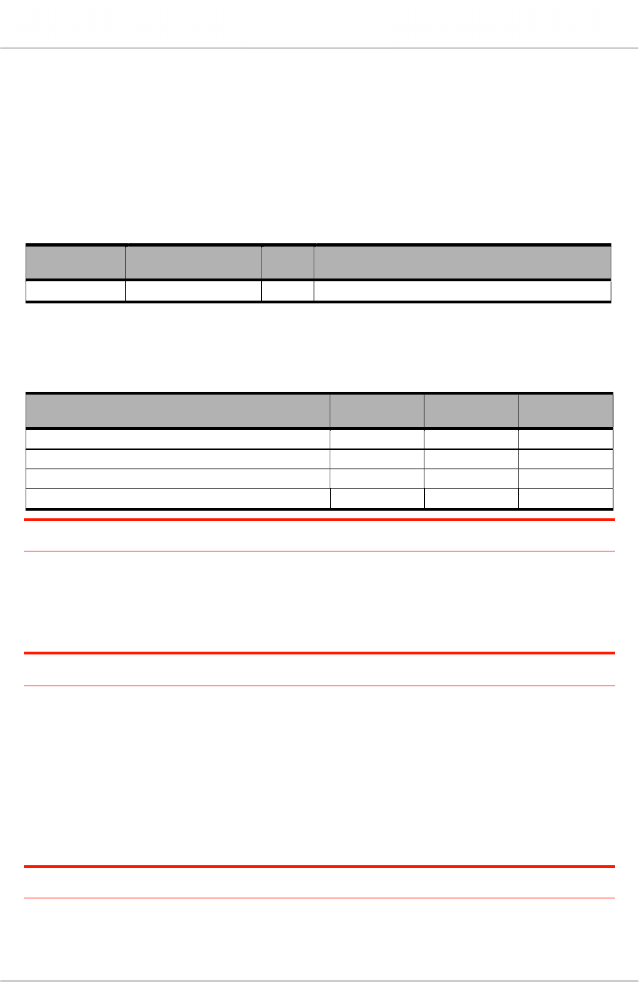
1. Introduction
This document is the Product Technical Specification for the AirPrime HL7650 Embedded Module. It
defines the high-level product features and illustrates the interfaces for these features. This document
is intended to cover the hardware aspects of the product, including electrical and mechanical.
The AirPrime HL7650 belongs to the AirPrime HL Series from Essential Connectivity Module family.
These are industrial grade Embedded Wireless Modules that provides data connectivity on LTE and
3G networks (as listed in Table 1 Supported Bands/Connectivity).
The HL7650 supports a large variety of interfaces such as USB 2.0, UART, Digital Audio, ADC, USIM
and GPIOs to provide customers with the highest level of flexibility in implementing high-end
solutions.
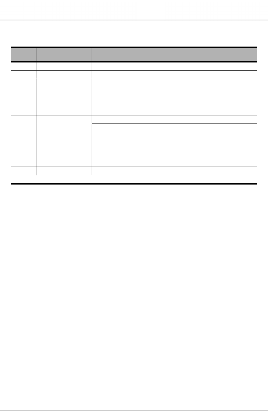
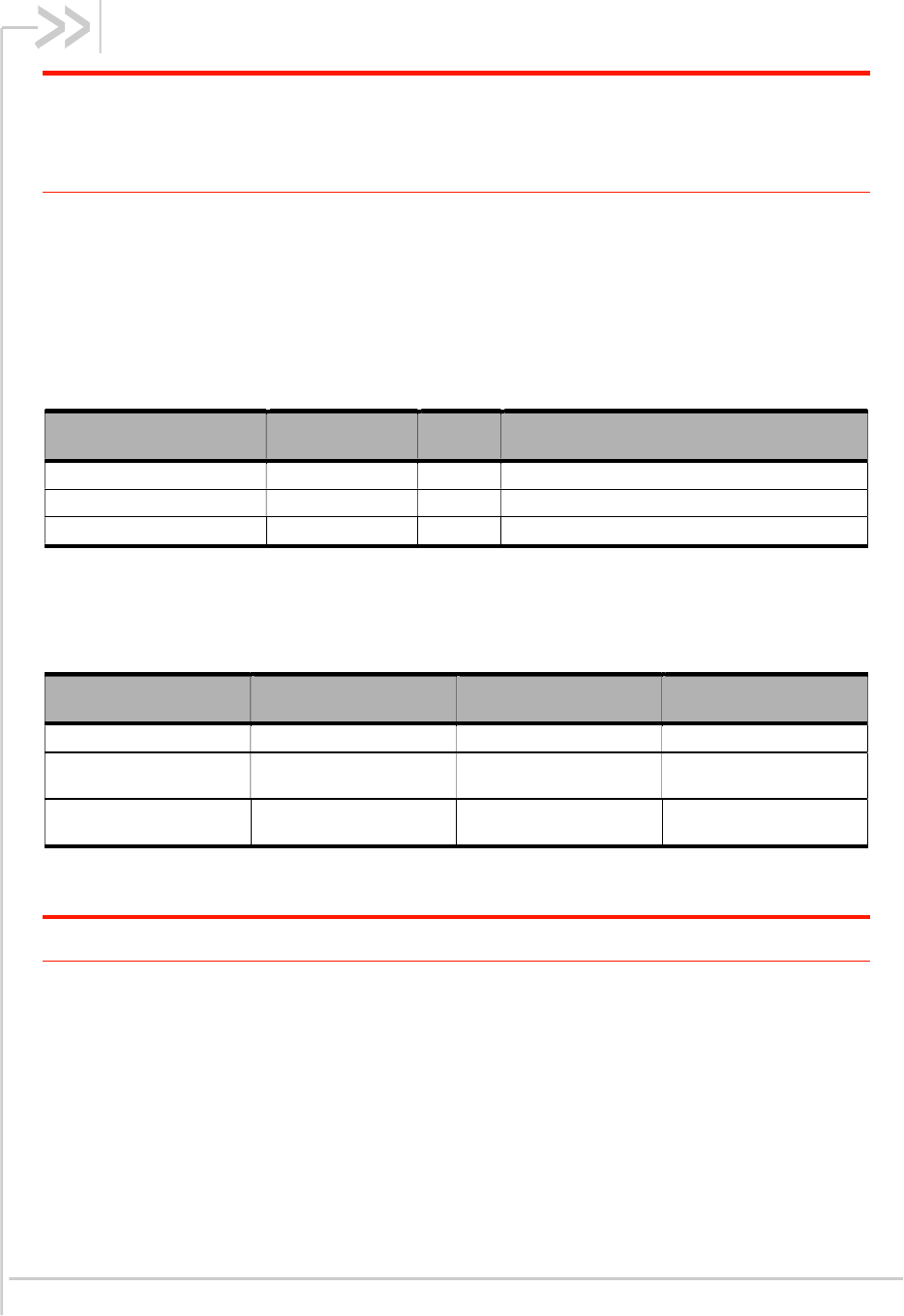
Table 1. Supported Bands/Connectivity
RF Band
Transmit Band (Tx) Receive Band (Rx) Maximum Output
Power
Uplink Downlink Uplink Downlink
LTE B3 1710 MHz 1785 MHz 1805 MHz 1880 MHz 23 dBm ± 2 dBm
LTE B5 824 MHz 849 MHz 869 MHz 894 MHz 23 dBm ± 2 dBm
LTE B8 880 MHz 915 MHz 925 MHz 960 MHz 23 dBm ± 2 dBm
LTE B28 703 MHz 748 MHz 758 MHz 808 MHz 23 dBm ± 2 dBm
UMTS B1 1920 MHz 1980 MHz 2110 MHz 2170 MHz 24 dBm +1 / -3 dBm
UMTS B5 824 MHz 849 MHz 869 MHz 894 MHz 24 dBm +1 / -3 dBm
UMTS B8 880 MHz 915 MHz 925 MHz 960 MHz 24 dBm +1 / -3 dBm
1.1. Common Flexible Form Factor (CF3)
The AirPrime HL7650 belongs to the Common Flexible Form Factor (CF3) family of modules. This
family consists of a series of WWAN modules that share the same mechanical dimensions (same
width and length with varying thicknesses) and footprint. The CF3 form factor provides a unique
solution to a series of problems faced commonly in the WWAN module space as it:
Accommodates multiple radio technologies (from 3G to LTE advanced) and band groupings
Supports bit-pipe (Essential Module Series) and value add (Smart Module Series) solutions
Offers electrical and functional compatibility
Provides Direct Mount as well as Socket-ability depending on customer needs
1.2. Physical Dimensions
AirPrime HL7650 modules are compact, robust, fully shielded modules with the following dimensions:
Length: 23 mm
Width: 22 mm
Thickness: 2.5 mm
Weight: 3.5 g
Note: Dimensions specified above are typical values.

41110363 Rev 4.0 October 18, 2017 11
Product Technical Specification Introduction
1.3. General Features
The table below summarizes the AirPrime HL7650 features.
Table 2. General Features
Feature Description
Physical
Small form factor (146-pad solderable LGA pad) – 23mm x 22mm x
2.5mm (nominal)
Metal shield can
RF connection pads (RF main interface)
Baseband signals connection
Electrical Single or double supply voltage (VBATT and VBATT_PA) – 3.2V – 4.5V
RF Quad-band LTE (B3, B5, B8 and B28) and tri-band UMTS (B1, B5 and B8)
USIM interface
Dual SIM Single Standby (DSSS)
1.8V/3V support
SIM extraction / hot plug detection
SIM/USIM support
Conforms to ETSI UICC Specifications.
Supports SIM application tool kit with proactive SIM commands
Note: Although UIM2 connectivity is available in the hardware, this feature is
not activated in the firmware.
Application interface
NDIS NIC interface support (Windows 7, Windows 8, Linux)
MBIM support
Multiple non-multiplexed USB channel support
Dial-up networking
USB selective suspend to maximize power savings
CMUX multiplexing over UART
AT command interface – 3GPP 27.007 standard, plus proprietary
extended AT commands
Protocol stack
LTE mode operation:
LTE FDD, bandwidth 1.4-20 MHz
System Release: 3GPP Rel. 9
Category 1 (up to 10 Mbit/s in downlink, 5 Mbit/s in uplink)
Rx Diversity
Max modulation 64 QAM DL, 16 QAM UL
Intra-frequency and inter-frequency mobility
SON ANR
Public Warning System PWS
HSDPA (High Speed Downlink Packet Access)
Compliant with 3GPP Rel. 8
Category 10 (10.1Mbps)
IPv6 support
HSUPA (High Speed Uplink Packet Access)
Compliant with 3GPP Release 8
Category 6 (5.76Mbps)

41110363 Rev 4.0 October 18, 2017 12
Product Technical Specification Introduction
Feature Description
SMS
SMS over SGs and IMS
SMS MO and MT
SMS saving to SIM card or ME storage
SMS reading from SIM card or ME storage
SMS sorting
SMS concatenation
SMS Status Report
SMS replacement support
SMS storing rules (support of
AT+CNMI
,
AT+CNMA
)
Connectivity
Multiple (up to 20) cellular packet data profiles
Sleep mode for minimum idle power draw
Mobile-originated PDP context activation / deactivation
Support QoS profile
Release 97 – Precedence Class, Reliability Class, Delay Class,
Peak Throughput, Mean Throughput
Release 99 QoS negotiation – Background, Interactive, and
Streaming
Static and Dynamic IP address. The network may assign a fixed IP
address or dynamically assign one using DHCP (Dynamic Host
Configuration Protocol).
Supports PAP and CHAP authentication protocols
PDP context type (IPv4, IPv6, IPv4v6). IP Packet Data Protocol context
RFC1144 TCP/IP header compression
Environmental
Operating temperature ranges (industrial grade):
Class A: -30°C to +70°C
Class B: -40°C to +85°C
RTC Real Time Clock (RTC) with calendar
41110363 Rev 4.0 October 18, 2017 13
Product Technical Specification Introduction
1.4. Architecture
The figure below presents an overview of the AirPrime HL7650 internal architecture and external
interfaces.
AirPrime HL7650
SAW
Filters
26MHz 32.768KHz
UART1 (8 pins)
VBAT T
GND
VGPIO
BAT_RTC
GPIO x 12
RESET _IN_ N
RF Main
JTAG
LGA-
146
Baseband
USIM1
MCU DSP
PMU RF
Analog Baseband
Peripherals
LGA-
146
26M_CLKOUT
32K_CLKOUT
PWR_ON_N
Dulpexer
PA
USB
Antenna
Switch
Antenna
Switch
RX_LTE
RF
RF DIV
TX_LTE
RF
RX_LTE
TX_ON
ADC x 2
Memory
(Flash + RAM)
USIM2
PCM
Figure 1. Architecture Overview
1.5. Interfaces
The AirPrime HL7650 module provides the following interfaces and peripheral connectivity:
1x – VGPIO
1x – BAT_RTC Backup Battery Interface
2x – 1.8V/3V USIM
1x – USB 2.0
12x – GPIOs (1 of which is multiplexed)
1x – 8-wire UART
1x – Active Low PWR_ON_N
1x – Active Low RESET_IN_N
2x – ADC
2x – System Clock out (32.768 KHz and 26 MHz)
1x – Digital Audio Interface (PCM)
1x – JTAG Interface
1x – RF Main Antenna
1x – RF Diversity
1x – TX Indicator
41110363 Rev 4.0 October 18, 2017 14
Product Technical Specification Introduction
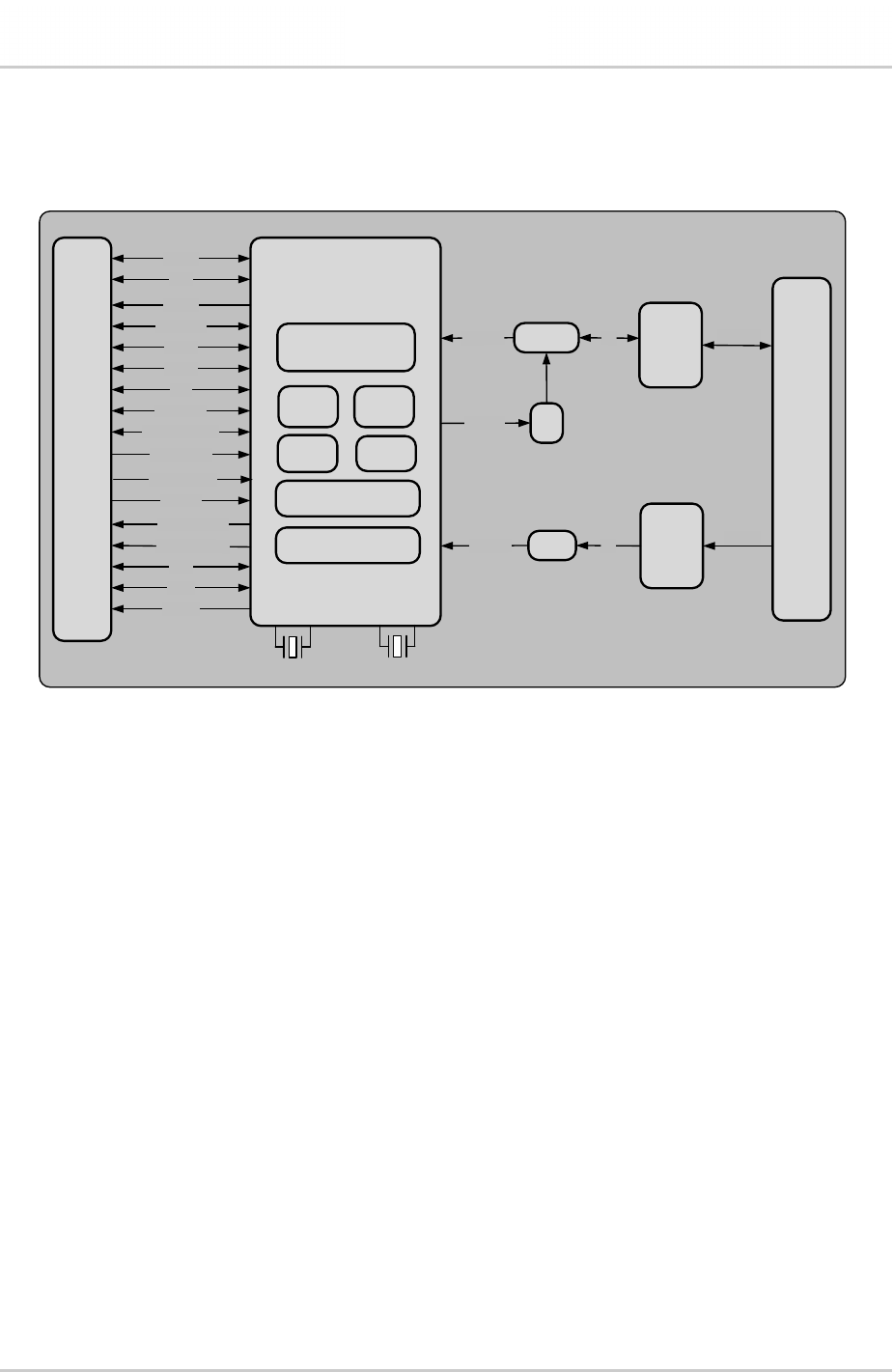
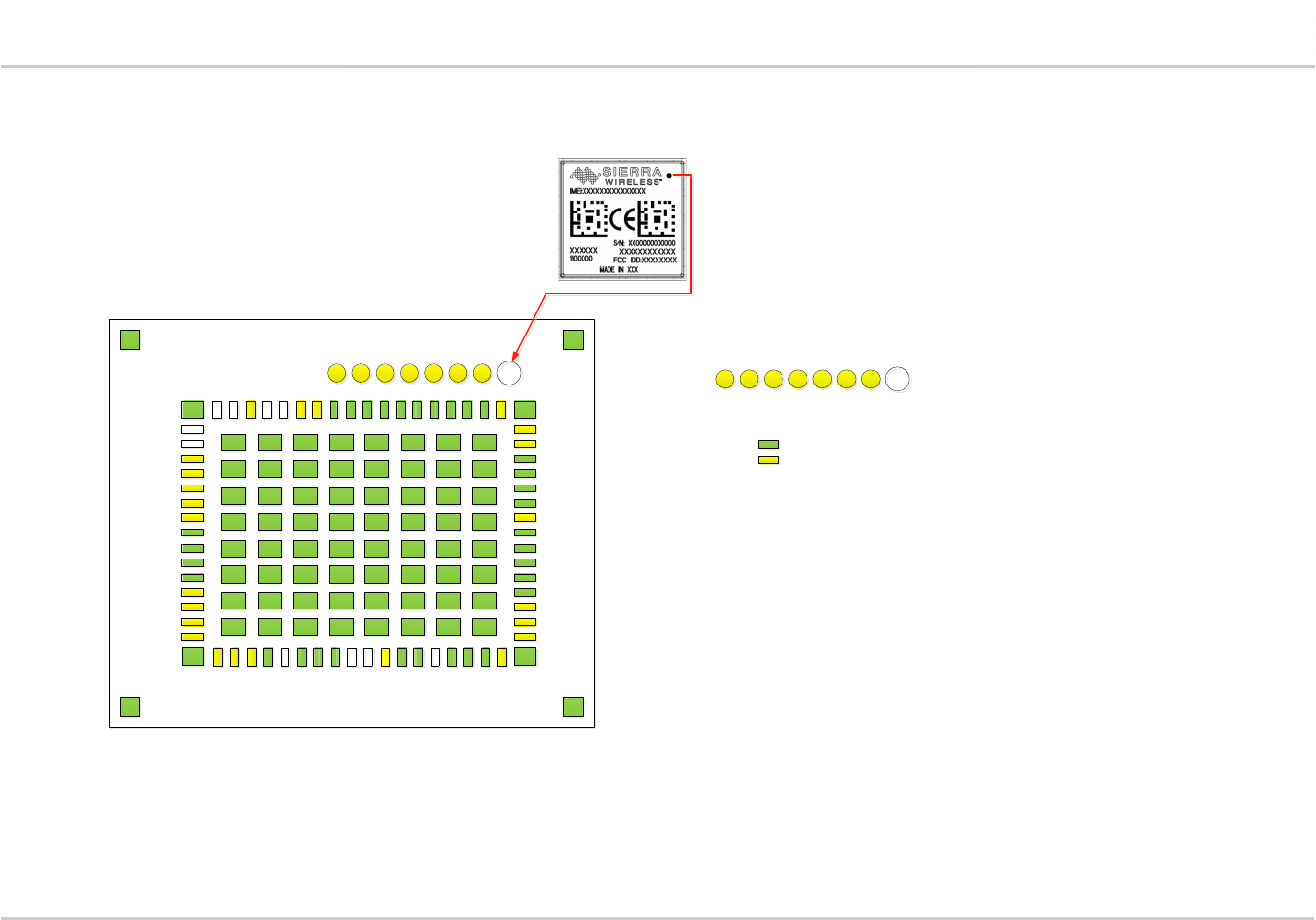
1.6. Connection Interface
The AirPrime HL7650 module is an LGA form factor device. All electrical and mechanical connections
are made through the 146 Land Grid Array (LGA) pads on the bottom side of the PCB.
Figure 2. Mechanical Overview (Top and Bottom Views)
The 146 pads have the following distribution:
66 inner signal pads, 1x0.5mm, pitch 0.8mm
1 reserved test point (do not connect), 1.0mm diameter
7 test point (JTAG), 0.8mm diameter, 1.20mm pitch
64 inner ground pads, 1.0x1.0mm, pitch 1.825mm/1.475mm
4 inner corner ground pads, 1x1mm
4 outer corner ground pads, 1x0.9mm
Figure 3. AirPrime HL7650 Top View
Figure 4. AirPrime HL7650 Bottom View
41110363 Rev 4.0 October 18, 2017 15
Product Technical Specification Introduction
1.7. ESD
Refer to the following table for ESD Specifications.
Table 3. ESD Specifications
Category Connection Specification
Operational RF ports IEC-61000-4-2 — Level (Electrostatic Discharge Immunity Test)
Non-operational Host connector
interface
Unless otherwise specified:
JESD22-A114 ± 1kV Human Body Model
JESD22-A115 ± 200V Machine Model
JESD22-C101C ± 250V Charged Device Model
Signals
USIM connector Adding ESD protection is highly recommended at the point where
the USIM contacts are exposed, and for any other signals that
would be subjected to ESD by the user.
Other host signals
1.8. Environmental and Certifications
1.8.1. Environmental Specifications
The environmental specification for both operating and storage conditions are defined in the table
below.
Table 4. Environmental Specifications
Conditions Range
Operating Class A -30°C to +70°C
Operating Class B -40°C to +85°C
Storage -40°C to +85°C
Class A is defined as the operating temperature ranges that the device:
Shall exhibit normal function during and after environmental exposure.
Shall meet the minimum requirements of 3GPP or appropriate wireless standards.
Class B is defined as the operating temperature ranges that the device:
Shall remain fully functional during and after environmental exposure
Shall exhibit the ability to establish an SMS or DATA call (emergency call) at all times even
when one or more environmental constraint exceeds the specified tolerance.
Unless otherwise stated, full performance should return to normal after the excessive
constraint(s) have been removed.

41110363 Rev 4.0 October 18, 2017 16
Product Technical Specification Introduction
1.8.2. Regulatory
Sierra Wireless hereby declares that the HL7650 is in compliance with all essential requirements of
Directive <TBD>.
The Declaration of Conformity will be available for viewing at the following location in the EU
community:
Sierra Wireless (UK) Limited
Suite 5, The Hub
Fowler Avenue
Farnborough Business Park
Farnborough, United Kingdom GU14 7JP
1.8.3. RoHS Directive Compliant
The AirPrime HL7650 module is compliant with RoHS Directive 2011/65/EU which sets limits for the
use of certain restricted hazardous substances. This directive states that “from 1st July 2006, new
electrical and electronic equipment put on the market does not contain lead, mercury, cadmium,
hexavalent chromium, polybrominated biphenyls (PBB) or polybrominated diphenyl ethers (PBDE)”.
1.8.4. Disposing of the Product
This electronic product is subject to the EU Directive 2012/19/EU for Waste Electrical
and Electronic Equipment (WEEE). As such, this product must not be disposed of at a
municipal waste collection point. Please refer to local regulations for directions on how
to dispose of this product in an environmental friendly manner.
1.9. References
[1] AirPrime HL Series Customer Process Guidelines
Reference Number: 4114330
[2] AirPrime HL76xx AT Commands Interface Guide
Reference Number: 4118395
[3] AirPrime HL Series Development Kit User Guide
Reference Number: 4114877
41110363 Rev 4.0 October 18, 2017 17
2. Pad Definition
AirPrime HL7650 pads are divided into 2 functional categories.
Core functions and associated pads cover all the mandatory features for M2M connectivity and will be available by default across all CF3 family of
modules. These Core functions are always available and always at the same physical pad location. A customer platform using only these functions
and associated pads is guaranteed to be forward and/or backward compatible with the next generation of CF3 modules.
Extension functions and associated pads bring additional capabilities to the customer. Whenever an Extension function is available on a module, it
is always at the same pad location.
Other pads marked as “not connected” or “reserved” should not be used.
Table 5. Pad Definition
Pad
# Signal Name Function I/O
I/O HW
Reset
State
Active
Low/High
Power
Supply
Domain
Recommendation
for Unused Pads Type
1 GPIO1 General purpose input/output I/O I, T - 1.8V Left Open Extension
2 UART1_RI UART1 Ring indicator O O, L - 1.8V Connect to test point Core
3 UART1_RTS UART1 Request to send I I, T/PU L 1.8V Connect to test point Core
4 UART1_CTS UART1 Clear to send O I, T/PU L 1.8V Connect to test point Core
5 UART1_TX UART1 Transmit data I I, T/PD - 1.8V Connect to test point Core
6 UART1_RX UART1 Receive data O I, T/PU - 1.8V Connect to test point Core
7 UART1_DTR UART1 Data terminal ready I I, T/PD L 1.8V Connect to test point Core
8 UART1_DCD UART1 Data carrier detect O O, L L 1.8V Connect to test point Core
9 UART1_DSR UART1 Data set ready O O, H L 1.8V Connect to test point Core
10 GPIO2 General purpose input/output I/O O, L - 1.8V Connect to test point Core
11 RESET_IN_N Input reset signal I N/A L 1.8V Left Open Core

41110363 Rev 4.0 October 18, 2017 18
Product Technical Specification Pad Definition
Pad
# Signal Name Function I/O
I/O HW
Reset
State
Active
Low/High
Power
Supply
Domain
Recommendation
for Unused Pads Type
12 USB_D- USB Data Negative (Low / Full Speed) I/O T - 3.3V Connect to test point Extension
USB Data Negative (High Speed) 0.38V
13 USB_D+ USB Data Positive (Low / Full Speed) I/O T - 3.3V Connect to test point Extension
USB Data Positive (High Speed) 0.38V
14 NC Not Connected - - - Not connected
15 NC Not Connected - - - Not connected
16 USB_VBUS USB VBUS I N/A - 5V Connect to test point Extension
17 NC Not Connected (Reserved for future use) - - - Left Open Not connected
18 NC Not Connected (Reserved for future use) - - - Left Open Not connected
19 NC Not Connected (Reserved for future use) - - - Left Open Not connected
20 NC Not Connected (Reserved for future use) - - - Left Open Not connected
21 BAT_RTC Power supply for RTC backup I/O N/A - 1.8V Left Open Extension
22 26M_CLKOUT 26MHz System Clock Output O I, T/PD - 1.8V Left Open Extension
23 32K_CLKOUT 32.768kHz System Clock Output O I, T/PD - 1.8V Left Open Extension
24 ADC1 Analog to digital converter I N/A - 1.2V Left Open Extension
25 ADC0 Analog to digital converter I N/A - 1.2V Left Open Extension
26 UIM1_VCC 1.8V/3V USIM1 Power supply O N/A - 1.8V/3V Mandatory connection Core
27 UIM1_CLK 1.8V/3V USIM1 Clock O O, L - 1.8V/3V Mandatory connection Core
28 UIM1_DATA 1.8V/3V USIM1 Data I/O O, L - 1.8V/3V Mandatory connection Core
29 UIM1_RESET 1.8V/3V USIM1 Reset O O, L L 1.8V/3V Mandatory connection Core
30 GND Ground 0V N/A - 0V Mandatory connection Extension
31 RF_DIV RF Input - Diversity - N/A - Mandatory connection Extension
32 GND Ground 0V N/A - 0V Mandatory connection Extension
33 PCM_OUT PCM data out O I, T/PD - 1.8V Left Open Extension
34 PCM_IN PCM data in I I, T/PD - 1.8V Left Open Extension
35 PCM_SYNC PCM sync out I/O I, T/PD - 1.8V Left Open Extension

41110363 Rev 4.0 October 18, 2017 19
Product Technical Specification Pad Definition
Pad
# Signal Name Function I/O
I/O HW
Reset
State
Active
Low/High
Power
Supply
Domain
Recommendation
for Unused Pads Type
36 PCM_CLK PCM clock I/O I, T/PD - 1.8V Left Open Extension
37 GND Ground 0V N/A - 0V Mandatory connection Core
38 NC Not Connected (Reserved for future use) - - - Left Open Not connected
39 GND Ground 0V N/A - 0V Mandatory connection Core
40 GPIO7 General purpose input/output I/O I, T/PD - 1.8V Left Open Core
41 GPIO8 General purpose input/output I/O O, L - 1.8V Connect to test point Core
42 NC Not Connected (Reserved for future use) - - - Left Open Not connected
43 NC Not Connected (Reserved for future use) - - - Left Open Not connected
44 GPIO13 General purpose input/output O I, T/PU - 1.8V Left Open Extension
45 VGPIO GPIO voltage output O N/A - 1.8V Left Open Core
46 GPIO6 General purpose input/output I/O I, T/PD - 1.8V Left Open Core
47 NC Not Connected (Reserved for future use) - - - Left Open Not connected
48 GND Ground 0V N/A - 0V Mandatory connection Core
49 RF_MAIN RF Input/output - N/A - Mandatory connection Core
50 GND Ground 0V N/A - 0V Mandatory connection Core
51 GPIO14 General purpose input/output I I, T/PU - 1.8V Left Open Extension
52 GPIO10 General purpose input/output I/O I, T/PD - 1.8V Left Open Extension
53 GPIO11 General purpose input/output I/O I, T/PD - 1.8V Left Open Extension
54 GPIO15 General purpose input/output I/O I, T/PU - 1.8V Left Open Extension
55 UIM2_VCC 1.8V/3V USIM2 Power supply O N/A - 1.8V/3V Mandatory connection Core
56 UIM2_DATA 1.8V/3V USIM2 Data I/O O, L - 1.8V/3V Mandatory connection Core
57 UIM2_RESET 1.8V/3V USIM2 Reset O O, L L 1.8V/3V Mandatory connection Core
58 UIM2_CLK 1.8V/3V USIM2 Clock O O, L 1.8V/3V Mandatory connection Core
59 PWR_ON_N Active Low Power On control signal I N/A L 1.8V Mandatory connection Core
60 TX_ON TX burst indicator O N/A 2.3V Left Open Extension
41110363 Rev 4.0 October 18, 2017 20
Product Technical Specification Pad Definition
Pad
# Signal Name Function I/O
I/O HW
Reset
State
Active
Low/High
Power
Supply
Domain
Recommendation
for Unused Pads Type
61 VBATT_PA Power supply (refer to section 3.1 Power
Supply for more information) I N/A -
3.2V (min)
3.7V (typ)
4.5V (max)
Mandatory connection Core
62 VBATT_PA Power supply (refer to section 3.1 Power
Supply for more information) I N/A -
3.2V (min)
3.7V (typ)
4.5V (max)
Mandatory connection Core
63 VBATT Power supply I N/A -
3.2V (min)
3.7V (typ)
4.5V (max)
Mandatory connection Core
64 UIM1_DET UIM1 Detection I/O I, T/PD H 1.8V Left Open Core
65 UIM2_DET/GPIO4 UIM2 Detection / General purpose
input/output I/O I, T/PD H 1.8V Left Open Extension
66 GPIO5 General purpose input/output I/O I, T - 1.8V Left Open Extension
67-70 GND Ground 0V N/A 0V Core
71 -
166 Note: These pads are not available on the AirPrime HL7650 module.
167 -
234 GND Ground 0V N/A - 0V Core
236 JTAG_RESET JTAG RESET I I, T L 1.8V Left Open Extension
237 JTAG_TCK JTAG Test Clock I I, PD - 1.8V Left Open Extension
238 JTAG_TDO JTAG Test Data Output O O, T - 1.8V Left Open Extension
239 JTAG_TMS JTAG Test Mode Select I I, PU - 1.8V Left Open Extension
240 JTAG_TRST JTAG Test Reset I I, PD L 1.8V Left Open Extension
241 JTAG_TDI JTAG Test Data Input I I, PU - 1.8V Left Open Extension
242 JTAG_RTCK JTAG Returned Test Clock O I, PD - 1.8V Left Open Extension

41110363 Rev 4.0 October 18, 2017 21
Product Technical Specification Pad Definition
2.1. Pad Types
Table 6. Pad Types
Type Definition
I Digital Input
O Digital Output
I/O Digital Input / Output
L Active High
H Active Low
T Tristate
T/PU Tristate with pull-up enabled
T/PD Tristate with pull-down enabled
N/A No Applicable
41110363 Rev 4.0 October 18, 2017 22
Product Technical Specification Pad Definition
2.2. Pad Configuration (Top View, Through Module)
168
169
167
170
18
17
16
15
14
13
12
11
10
9
8
7
6
4
3
2
1
5
66
65
64
63
62
61
60
59
34
35
36
37
38
38
39
40
41
42
42
43
43
44
45
46
48
49
50
51
47
47
58
57
56
55
53
52
54
70
67
19
20
21
22
23
24
25
26
27
28
29
30
32
33
31
69
68
192 193 194 195 196 197 198 171
191 214 215 216 217 218 199 172
190 213 228 229 230 219 200 173
189 212 227 234 231 220 201 174
188 211 226 233 232 221 202 175
187 210 225 224 223 222 203 176
186 209 208 207 206 205 204 177
185 184 183 182 181 180 179 178
236237238239240241242
GND
GPIO5
UIM2_DET / GPIO4
UIM1_DET
VBATT
VBATT_PA
VBATT_PA
TX_ON
PWR_ON_N
UIM2_CLK
UIM2_RESET
UIM2_DATA
UIM2_VCC
GPIO15
GPIO11
GPIO10
GND
GND
NC
NC
BAT_RTC
26M_CLKOUT
32K_CLKOUT
ADC1
ADC0
UIM1_VCC
UIM1_CLK
UIM1_DATA
UIM1_RESET
GND
RF_DIV
GND
PCM_OUT
GND
PCM_IN
PCM_SYNC
PCM_CLK
GND
NC
GND
GPIO7
GPIO8
NC
NC
GPIO13
VGPIO
GPIO6
NC
GND
RF_MAIN
GND
GPIO14
NC
NC
USB_VBUS
NC
NC
USB_D+
USB_D-
RESET_IN_N
GPIO2
UART1_DSR
UART1_DCD
UART1_DTR
UART1_RX
UART1_TX
UART1_CTS
UART1_RTS
UART1_RI
GPIO1
JTAG_RTCK
JTAG_TDI
JTAG_TRST
JTAG_TMS
JTAG_TDO
JTAG_TCK
JTAG_RESET
Core pad
Extension pad
236237238239240241242
Figure 5. Pad Configuration
41110363 Rev 4.0 October 18, 2017 23
3. Detailed Interface Specifications
Note: If not specified, all electrical values are given for VBATT=3.7V and an operating temperature of
25°C.
For standard applications, VBATT and VBATT_PA must be tied externally to the same power
supply. For some specific applications, AirPrime HL7650 module supports separate VBATT and
VBATT_PA connection if requirements below are fulfilled.
3.1. Power Supply
The AirPrime HL7650 module is supplied through the VBATT and VBATT_PA signals.
Refer to the following table for the pad description of the Power Supply interface.
Table 7. Power Supply Pad Description
Pad Number Signal Name I/O Description
63 VBATT I Power supply (base band)
61, 62 VBATT_PA I Power supply (radio frequency)
37, 39, 48, 67-70, 167-234 GND Ground
Refer to the following table for the electrical characteristics of the Power Supply interface.
Table 8. Power Supply Electrical Characteristics
Supply Minimum Typical Maximum
VBATT voltage (V) 3.21 3.7 4.5
VBATT_PA voltage (V)
Full Specification 3.21 3.7 4.5
VBATT_PA voltage (V)
Extended Range 2.82 3.7 4.5
1 This value has to be guaranteed during the burst
2 No guarantee of 3GPP performances over extended range
Note: Load capacitance for VBATT is around 140µF ± 20% embedded inside the module.
Load capacitance for VBATT_PA is around 20µF ± 20% embedded inside the module.
41110363 Rev 4.0 October 18, 2017 24
Product Technical Specification Detailed Interface Specifications
3.2. Current Consumption
The following table lists the current consumption of the AirPrime HL7650 at different conditions.
Note: Typical values are defined for VBATT/VBATT_PA at 3.7V and 25°C, for 50Ω impedance at all RF
ports with VSWR1:1 and CMW500. Maximum values are defined with worst conditions among
supported ranges of voltages and temperature (50Ω, VSWR1:1 and CMW500).
Table 9. Current Consumption
Parameter Typical Maximum Unit
Off mode 110 300 µA
Sleep mode – LTE
DRX8
USB disconnected
Band 3 1.7 5.5 mA
Band 5 1.9 6.0 mA
Band 8 1.7 5.7 mA
Band 28 1.9 6.0 mA
Sleep mode – WCDMA
DRX8
USB disconnected
Band 1 1.2 4.95 mA
Band 5 1.2 4.95 mA
Band 8 1.2 4.95 mA
LTE in communication mode
(TX Max)
Band 3 595 740 mA
Band 5 585 730 mA
Band 8 665 815 mA
Band 28 765 920 mA
WCDMA in communication
mode (TX Max)
Band 1 515 630 mA
Band 5 490 605 mA
Band 8 490 610 mA
Note: Maximum current peak measured for VSWR3:1 is 1100 mA.
Table 10. Current Consumption per Power Supply
Parameter (at nominal voltage, 3.7 V) Typical Maximum Unit
VBATT
LTE in
communication mode
(TX Max)
Band 3 235 355 mA
Band 5 230 355 mA
Band 8 235 380 mA
Band 28 240 380 mA
WCDMA in
communication mode
(TX Max)
Band 1 130 230 mA
Band 5 125 220 mA
Band 8 125 220 mA
VBATT_PA
LTE in
communication mode
(TX Max)
Band 3 360 385 mA
Band 5 355 375 mA
Band 8 430 435 mA
Band 28 525 540 mA
WCDMA in
communication mode
(TX Max)
Band 1 385 400 mA
Band 5 365 385 mA
Band 8 365 390 mA
41110363 Rev 4.0 October 18, 2017 25
Product Technical Specification Detailed Interface Specifications
3.3. VGPIO
The VGPIO output can be used to:
Pull-up signals such as I/Os
Supply the digital transistors driving LEDs
The VGPIO output is available when the AirPrime HL7650 module is switched ON.
Refer to the following table for the pad description of the VGPIO interface.
Table 11. VGPIO Pad Description
Pad Number
Signal Name
I/O
Description
45 VGPIO O GPIO voltage output
Refer to the following table for the electrical characteristics of the VGPIO interface.
Table 12. VGPIO Electrical Characteristics
Parameter Minimum Typical Maximum Remarks
Voltage level (V) 1.7 1.8 1.9 Both active mode and sleep mode
Current capability
Active Mode (mA) - - 50 Power management support up to
50mA output in Active mode
Current capability
Sleep Mode (mA) - - 3 Power management support up to
3mA output in Sleep mode
Rise Time (ms) - - 1.5 Start-Up time from 0V
3.4. BAT_RTC
The AirPrime HL7650 module provides an input/output to connect a Real Time Clock power supply.
This pad is used as a back-up power supply for the internal Real Time Clock. The RTC is supported
when VBATT is available but a back-up power supply is needed to save date and hour when VBATT
is switched off.
If VBATT is available, the back-up battery can be charged by the internal 1.8V power supply regulator.
Refer to the following table for the pad description of the BAT_RTC interface.
Table 13. BAT_RTC Pad Description
Pad Number
Signal Name
I/O
Description
21 BAT_RTC I/O Power supply for RTC backup
Refer to the following table for the electrical characteristics of the BAT_RTC interface.
41110363 Rev 4.0 October 18, 2017 26
Product Technical Specification Detailed Interface Specifications
Table 14. BAT_RTC Electrical Characteristics
Parameter Minimum Typical Maximum Unit
Input voltage 1.7 1.8 1.9 V
Input current consumption - 2.5 (TBC) - µA
Output voltage -5% 1.8 +5% V
Max charging current (@VBATT=3.7V) - 25 (TBC) - mA
3.5. USIM Interface
The AirPrime HL7650 has two physical USIM interfaces, UIM1 and UIM2.
Both UIM1 and UIM2 allow control of a 1.8V/3V USIM and is fully compliant with GSM 11.11
recommendations concerning SIM functions.
The five signals used by the UIMx interface are as follows:
UIMx_VCC: Power supply
UIMx_CLK: Clock
UIMx_DATA: I/O port
UIMx_RESET: Reset
UIMx_DET: Hardware SIM detection
UIM1 is used in single SIM applications, and has optional support for dual SIM applications with an
external SIM switch (for use in Dual SIM Single Standby (DSSS) applications).
A second UIM interface, UIM2, is also available for Dual SIM Single Standby (DSSS) option.
Note: Although UIM2 connectivity is available in the hardware, this feature is not activated in the firmware.
For USIM design examples, refer to section 5.9 USIM Application.
Refer to the following table for the pad description of both UIM interfaces.
Table 15. UIM1 Pad Description
Pad Number Signal Name Description Multiplex
26 UIM1_VCC 1.8V/3V USIM1 Power
supply
27 UIM1_CLK 1.8V/3V USIM1 Clock
28 UIM1_DATA 1.8V/3V USIM1 Data
29 UIM1_RESET 1.8V/3V USIM1 Reset
64 UIM1_DET USIM1 Detection
Table 16. UIM2 Pad Description
Pad Number Signal Name Description Multiplex
55 UIM2_VCC 1.8V/3V USIM2 Power supply
58 UIM2_CLK 1.8V/3V USIM2 Clock
56 UIM2_DATA 1.8V/3V USIM2 Data
41110363 Rev 4.0 October 18, 2017 27
Product Technical Specification Detailed Interface Specifications
Pad Number Signal Name Description Multiplex
57 UIM2_RESET 1.8V/3V USIM2 Reset
65 UIM2_DET USIM2 Detection GPIO4
Refer to the following table for the electrical characteristics of both UIM1 and UIM2 interfaces.
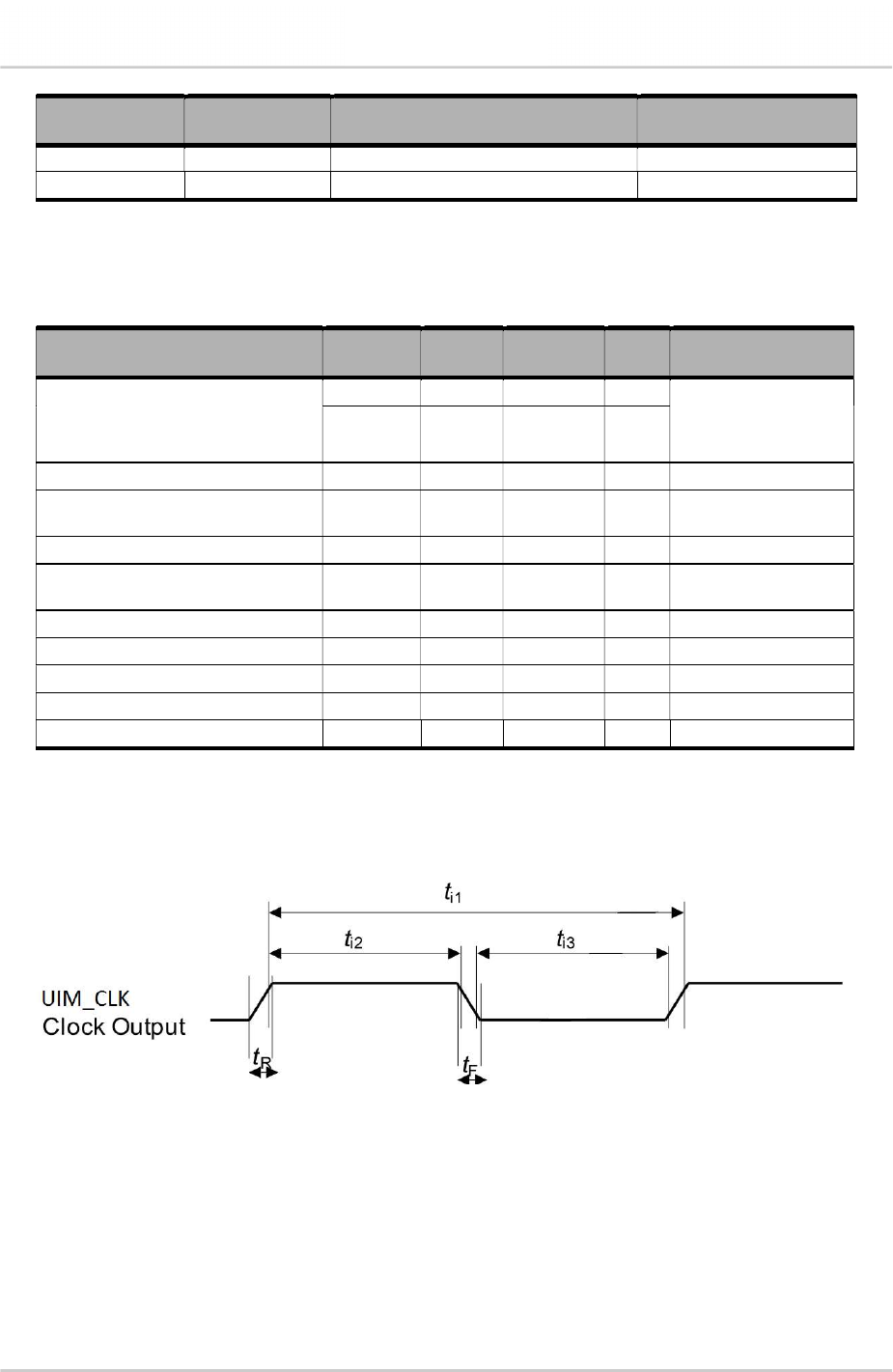
Table 17. UIM1 and UIM2 Electrical Characteristics
Parameter Minimum Typical
Maximum
Units
Remarks
UIMx Interface Voltage
(VCC, CLK, IO, RESET)
- 2.9 - V The appropriate
output voltage is auto
detected and selected
by software.
- 1.80 - V
UIMx Detect - 1.80 - V High active
UIMx_VCC Current - - 10 mA Max output current in
sleep mode = 3 mA
UIMx_VCC Line Regulation - - 50 mV/V At Iout_Max
UIMx_VCC Power-up Setting Time
from power down - 10 - µs
UIMx_CLK clock period (t
i1
) 205 307 - ns
UIMx_CLK high time (t
i2
) 82 - - ns
UIMx_CLK high time (t
i3
) 82 - - ns
UIMx_CLK rise time/fall time (t
R
/ t
F
) - - 50 ns
UIMx_IO rise time/fall time (t
R
/ t
F
) - - 1000 ns
3.5.1. UIMx_CLK
The following figure shows the UIMx_CLK timing waveform.
Figure 6. UIMx Timing Waveform
3.5.2. UIMx_DET
UIMx_DET is used to detect and notify the application about the insertion and removal of a USIM
device in the USIM socket connected to the USIM interface (UIM1 or UIM2). When a USIM is
inserted, the state of UIMx_DET transitions from logic 0 to logic 1. Inversely, when a USIM is
removed, the state of UIMx_DET transitions from logic 1 to logic 0.
While UIM1_DET has a dedicated pad (pad 64), UIM2_DET is multiplexed with GPIO4 (pad 65).
41110363 Rev 4.0 October 18, 2017 28
Product Technical Specification Detailed Interface Specifications
Enabling or disabling this UIM detect feature can be done using the
AT+KSIMDET
command. For more
information about this command, refer to document [2] AirPrime HL76xx AT Commands Interface
Guide.
3.6. USB Interface
The AirPrime HL7650 has one Universal Serial Bus interface complaint with USB Rev 2.0.
Refer to the following table for the pad description of the USB interface.
Table 18. USB Pad Description
Pad Number Signal Name I/O Function
12 USB_D- I/O USB Data Negative
13 USB_D+ I/O USB Data Positive
16 USB_VBUS I USB VBUS
Note: When the 5V USB supply is not available, connect USB_VBUS to VBATT to supply the USB
interface.
Refer to the following table for the electrical characteristics of the USB interface.
Table 19. USB Electrical Characteristics
Parameter Minimum Typical Maximum Units Test Condition
Input voltage at pads
USB_D+ / USB_D- -0.3 - 3.6 V
Voltage USB_VBUS 0 - 5.25 V
Full Speed Mode
Signal Rate 11.994 - 12.006 Mbit/s
EOP (end of packet) Width 160 - 175 ns
Rising Edge 4 - 20 ns At 10% and 90%
Falling Edge 4 - 20 ns At 10% and 90%
High Speed Mode
Signal Rate 479.760 - 480.024 Mbit/s
EOP (end of packet) Width 15.625 - 17.7073 ns
Rising Edge 500 - ps At 10% and 90%
Falling Edge 500 - ps At 10% and 90%
41110363 Rev 4.0 October 18, 2017 29
Product Technical Specification Detailed Interface Specifications
3.7. Electrical Information for Digital I/O
The AirPrime HL7650 supports two groups of digital interfaces with varying current drain limits. The
following list enumerates these interfaces.
Group 1 (6mA current drain limit)
GPIO2, GPIO4, GPIO6, GPIO8, GPIO10, GPIO11, GPIO13, GPIO14, GPIO15
Group 2 (1mA current drain limit)
GPIO1, GPIO5, GPIO7
UART1
JTAG
Refer to the following table for the electrical characteristics of the Digital I/O interface.
Table 20. Digital I/O Electrical Characteristics
Parameter Symbol Minimum Maximum Remarks
Input Current-High (µA) I
IH
- -240
Input Current-Low (µA) I
IL
- 240
Group 1 DC Output Current-High (mA) I
OH
- 6
DC Output Current-Low (mA) I
OL
-6 -
Group 2 DC Output Current-High (mA) I
OH
- 1
DC Output Current-Low (mA) I
OL
-1 -
Input Voltage-High (V) V
IH
1.33 1.90
Input Voltage-Low (V) V
IL
-0.20 0.34
Output Voltage-High (V) V
OH
1.45 - I
OH
= -6mA
V
OH
1.60 - I
OH
= -0.1mA
Output Voltage-Low (V) V
OL
- 0.35 I
OL
= 6mA
V
OL
- 0.20 I
OL
= 0.1mA
3.8. General Purpose Input/Output (GPIO)
The AirPrime HL7650 module provides 12 GPIOs, 1 of which is multiplexed.
Refer to the following table for the pad description of the GPIO interface.
Table 21. GPIO Pad Description
Pad Number Signal Name Multiplex I/O Power Supply Domain
1 GPIO1 I/O 1.8V
10 GPIO2 I/O 1.8V
40 GPIO7 I/O 1.8V
41 GPIO8 I/O 1.8V
44 GPIO13 I/O 1.8V
41110363 Rev 4.0 October 18, 2017 30
Product Technical Specification Detailed Interface Specifications
Pad Number Signal Name Multiplex I/O Power Supply Domain
46 GPIO6 I/O 1.8V
51 GPIO14 I/O 1.8V
52 GPIO10 I/O 1.8V
53 GPIO11 I/O 1.8V
54 GPIO15 I/O 1.8V
65 GPIO4 UIM2_DET I/O 1.8V
66 GPIO5 I/O 1.8V
3.9. Main Serial Link (UART1)
The main serial link (UART1) is used for communication between the AirPrime HL7650 module and a
PC or host processor. It consists of a flexible 8-wire serial interface that complies with RS-232
interface.
The supported baud rates of the UART1 are 300, 1200, 2400, 4800, 9600, 19200, 38400, 57600,
115200, 230400, 460800, 500000, 750000, 921600, 1843200, 3000000 and 3250000 bit/s.
The signals used by UART1 are as follows:
TX data (UART1_TX)
RX data (UART1_RX)
Request To Send (UART1_RTS)
Clear To Send (UART1_CTS)
Data Terminal Ready (UART1_DTR)
Data Set Ready (UART1_DSR)
Data Carrier Detect (UART1_DCD)
Ring Indicator (UART1_RI)
Note: Signal names are according to PC view.
Refer to the following table for the pad description of the main serial link (UART1) interface.
Table 22. UART1 Pad Description
Pad # Signal Name* I/O* Description
2 UART1_RI O Signal incoming calls (data only), SMS, etc.
3 UART1_RTS I Request to send
4 UART1_CTS O AirPrime HL7650 is ready to receive AT commands
5 UART1_TX I Transmit data
6 UART1_RX O Receive data
7 UART1_DTR I (active low)
Prevents the AirPrime HL7650 from entering sleep mode,
switches between data mode and command mode, and
wakes the module up.
8 UART1_DCD O Signal data connection in progress
9 UART1_DSR O Signal UART interface is ON
* According to PC view.
41110363 Rev 4.0 October 18, 2017 31
Product Technical Specification Detailed Interface Specifications
3.10. POWER-ON Signal (PWR_ON_N)
A low-level signal has to be provided to switch the AirPrime HL7650 module ON.
It is internally connected to the permanent 1.8V supply regulator inside the HL7650 via a pull-up
resistor. Once VBAT is supplied to the HL7650 module, this 1.8V supply regulator will be enabled and
so the PWR_ON_N signal is by default at high level.
Refer to the following table for the pad description of the PWR_ON_N interface.
Table 23. PWR_ON_N Pad Description
Pad Number
Signal Name
I/O
Description
59 PWR_ON_N I Power On the HL7650 module
Refer to the following table for the electrical characteristics of the PWR_ON_N interface.
Table 24. PWR_ON_N Electrical Characteristics
Parameter Minimum Typical Maximum
Input Voltage-Low (V) - 0.51
Input Voltage-High (V) 1.33 - 2.2
Power-up period (ms) from PWR_ON_N falling edge 2000 - -
PWR_ON_N assertion time (ms) 25
Note: As PWR_ON_N is internally pulled up with 100kΩ, an open collector or open drain transistor must
be used for ignition.
VGPIO is an output from the module that can be used to check if the module is active.
When VGPIO = 0V, the module is OFF
When VGPIO = 1.8V, the module is ON (it can be in idle, communication or sleep mode)
Note: PWR_ON_N signal cannot be used to power the module off. To power the module off, use AT
command
AT+CPWROFF
.
3.11. Reset Signal (RESET_IN_N)
To reset the module, a low-level pulse must be sent on the RESET_IN_N pad for 20ms. This action
will immediately restart the AirPrime HL7650 module with the PWR_ON_N signal at low level. (If the
PWR_ON_N signal is at high level, the module will be powered off.) As RESET_IN_N is internally
pulled up, an open collector or open drain transistor should be used to control this signal.
The RESET_IN_N signal will reset the registers of the CPU and reset the RAM memory as well, for
the next power on.
Note: As RESET_IN_N is referenced to the VRTC (200kΩ pull-up resistor to VRTC 1.8V) an open
collector or open drain transistor has to be used to control this signal.
Refer to the following table for the pad description of the RESET_IN_N interface.
41110363 Rev 4.0 October 18, 2017 32
Product Technical Specification Detailed Interface Specifications
Table 25. RESET_IN_N Pad Description
Pad Number
Signal Name
I/O
Description
12 RESET_IN_N I Hardware Reset
Refer to the following table for the electrical characteristics of the RESET_IN_N interface.
Table 26. RESET_IN_N Electrical Characteristics
Parameter Minimum Typical Maximum
Input Voltage-Low (V) - 0.51
Input Voltage-High (V) 1.33 - 2.2
Reset assertion time (ms) 20 - -
Power-up period (ms) from RESET_IN_N falling edge* 2000 - -
* With the PWR_ON_N Signal at low level.
3.12. Analog to Digital Converter (ADC)
Two Analog to Digital Converter inputs, ADC0 and ADC1, are provided by the AirPrime HL7650
module. These converters are 10-bit resolution ADCs ranging from 0 to 1.2V.
Typical ADC use is for monitoring external voltage, wherein an application is used to safely power
OFF an external supply in case of overvoltage.
Refer to the following table for the pad description of the ADC interface.
Table 27. ADC Pad Description
Pad Number
Signal Name
I/O
Description
24 ADC1 I Analog to digital converter
25 ADC0 I Analog to digital converter
Refer to the following table for the electrical characteristics of the ADC interface.
Table 28. ADC Electrical Characteristics
Parameter Minimum Typical Maximum Remarks
ADCx Resolution (bits) - 10 -
Input Voltage Range (V) 0 - 1.2 General purpose input
Update rate per channel (kHz) - - 125
Integral Nonlinearity (bits) - - ± 2 LSB
Offset Error (bits) - - ± 1 LSB
Gain 849 853 858
Absolute gain drift - - ± 0.05
Input Resistance (MΩ) 1 - -
Input Capacitance (pF) - 1 -
41110363 Rev 4.0 October 18, 2017 33
Product Technical Specification Detailed Interface Specifications
Parameter Minimum Typical Maximum Remarks
Current tolerance - - ± 3%
Quiescent current (µA) - 710 -
Wake-up time from power save (µs) - 50 -
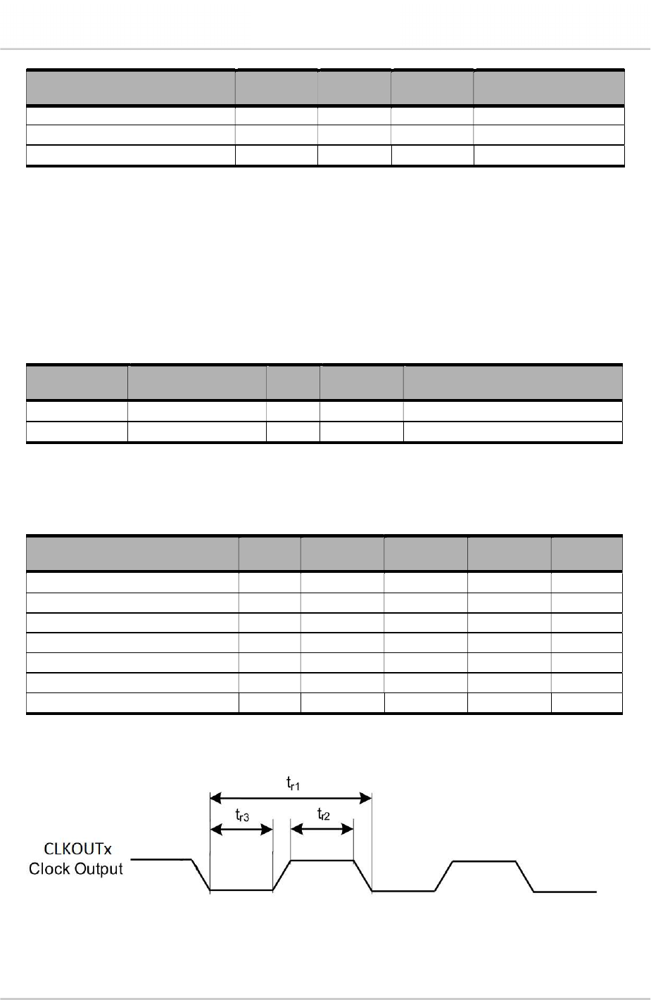
3.13. Clock Out Interface
The AirPrime HL7650 module supports two digital clock out interfaces.
Enabling or disabling the clock out feature can be done using AT commands. For more information
about AT commands, refer to document [2] AirPrime HL76xx AT Commands Interface Guide.
Refer to the following table for the pad description of the clock out interface.
Table 29. Clock Out Interface Pad Description
Pad Number Signal Name I/O I/O Type Description
22 26M_CLKOUT O 1.8V 26MHz Digital Clock output
23 32K_CLKOUT O 1.8V 32.768kHz Digital Clock output
Refer to the following table for the electrical characteristics of the clock out interface.
Table 30. Clock Out Interface Electrical Characteristics
Parameter Symbol Minimum Typical Maximum Units
CLKOUTn period at 26MHz (t
r1
)
- 38 - ns
CLKOUTn low time at 26MHz (t
r2
)
10 - - ns
CLKOUTn high time at 26MHz (t
r3
)
10 - - ns
CLKOUTn period at 32.768KHz (t
r1
)
- - - ns
CLKOUTn low time at 32.768KHz (t
r2
)
- - - ns
CLKOUTn high time at 32.768KHz (t
r3
)
- - - ns
Period jitter - - 4 ns
The following figure shows the clock out (CLKOUT) timing waveform.
Figure 7. CLKOUTx Timing Waveform
41110363 Rev 4.0 October 18, 2017 34
Product Technical Specification Detailed Interface Specifications
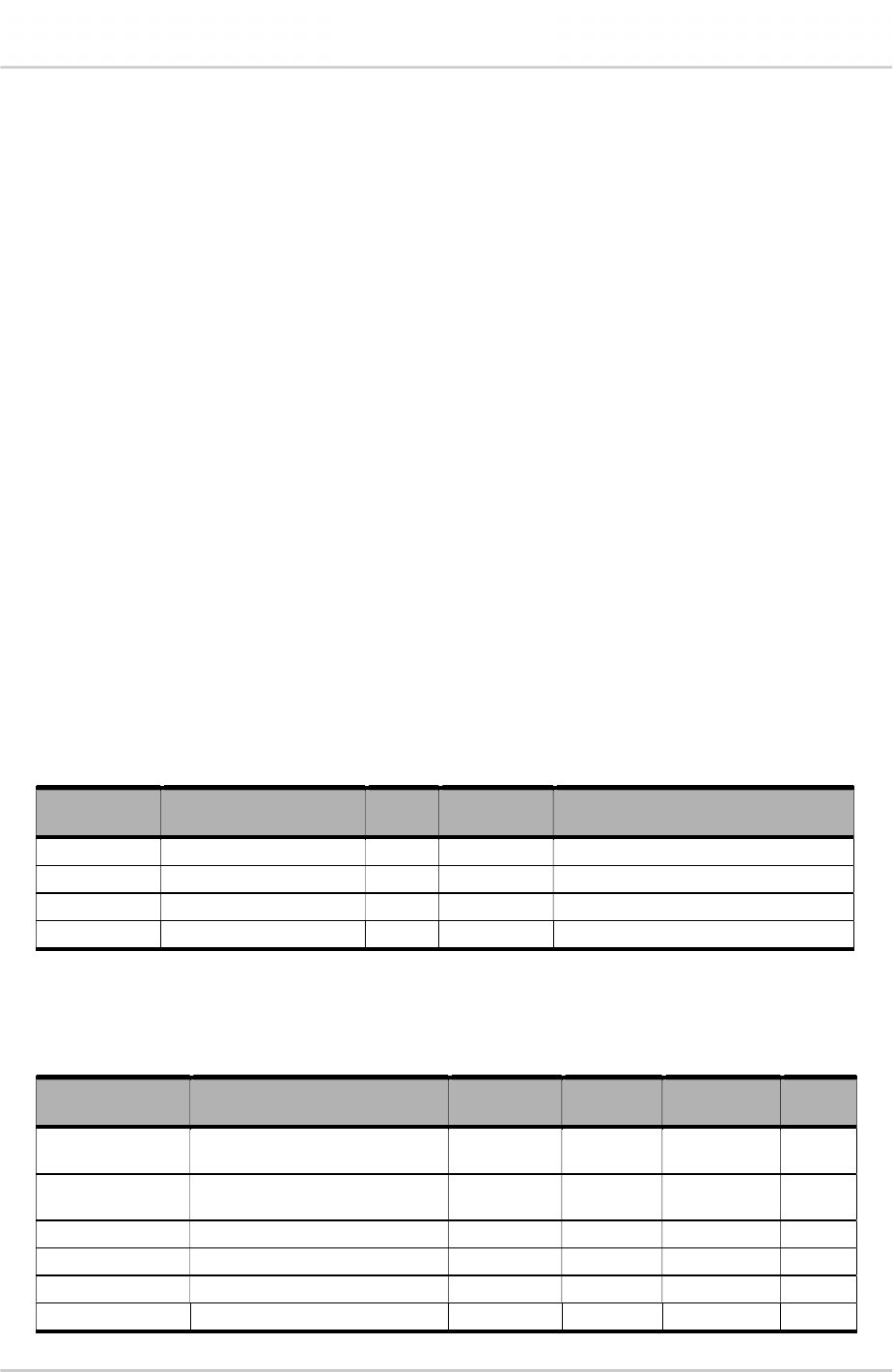
3.14. Digital Audio (PCM) Interface
The Digital Audio (PCM) Interface allows connectivity with standard audio peripherals. It can be used,
for example, to connect an external audio codec.
The programmability of this interface allows addressing a large range of audio peripherals.
The PCM interface is a high speed full duplex interface that can be used to send and receive digital
audio data to external audio ICs. The Digital Audio Interface also features the following:
PCM master or slave
16 bits data word length, linear mode
MSB first
Configurable PCM bit clock rate on 256kHz, 384kHz or 512kHz
Long frame sync
The signals used by the Digital Audio Interface are as follows:
PCM_SYNC: The frame synchronization signal delivers an 8 kHz frequency pulse that
synchronizes the frame data in and the frame data out.
PCM_CLK: The frame bit clock signal controls data transfer with the audio peripheral.
PCM_OUT: The frame “data out” relies on the selected configuration mode.
PCM_IN: The frame “data in” relies on the selected configuration mode.
Refer to the following table for the pad description of the digital audio interface.
Table 31. Digital Audio Pad Description
Pad # Signal Name I/O I/O Type Description
36 PCM_CLK O 1.8V PCM clock
35 PCM_SYNC O 1.8V PCM synchronization
34 PCM_IN I 1.8V PCM data in
33 PCM_OUT O 1.8V PCM data out
Refer to the following table for the electrical characteristics of the digital audio interface.
Table 32. Digital Audio Electrical Characteristics
Signal Description Minimum Typical Maximum Unit
Tsync_low +
Tsync_high PCM_SYNC frequency 8 KHz
Tsync_low +
Tsync_high PCM_SYNC period 125 µs
Tsync_low PCM_SYNC low time 124 µs
Tsync_high PCM_SYNC high time 1 µs
T
CLK-cycle
PCM_CLK period - 3.9 - µs
T
IN-setup
PCM_IN setup time 59.6 - - ns
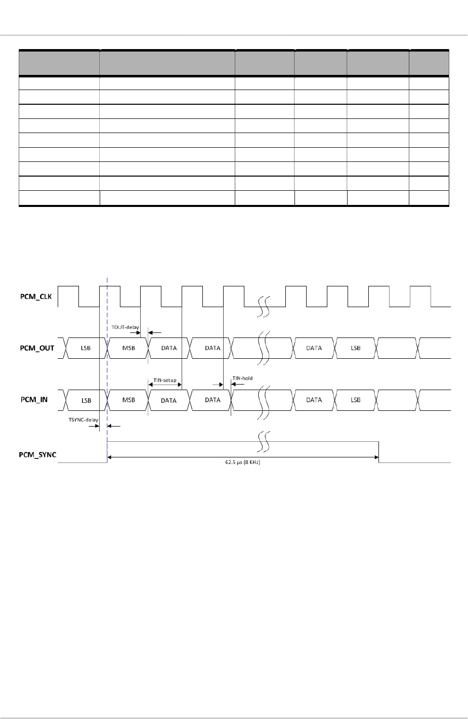
41110363 Rev 4.0 October 18, 2017 35
Product Technical Specification Detailed Interface Specifications
Signal Description Minimum Typical Maximum Unit
T
IN-hold
PCM_IN hold time 12 - - ns
T
OUT-delay
PCM_OUT delay time - - 21.6 ns
T
SYNC-delay
PCM_SYNC output delay -24 - 31.2 ns
VDD PCM Signaling Voltage 1.7 1.8 1.9 V
V
IH
I/O Voltage input low 0.35*VDD - VDD+0.3 V
V
IL
I/O Voltage input high -0.3 - 0.65*VDD V
V
OL
I/O Voltage output low - - 0.45 V
V
OH
I/O Voltage output high VDD-0.45 - - V
I
L
I/O Leakage current - - ±0.7 µA
3.14.1. PCM Waveforms
The following figure shows the PCM timing waveform.
Figure 8. PCM Timing Waveform
41110363 Rev 4.0 October 18, 2017 36
Product Technical Specification Detailed Interface Specifications
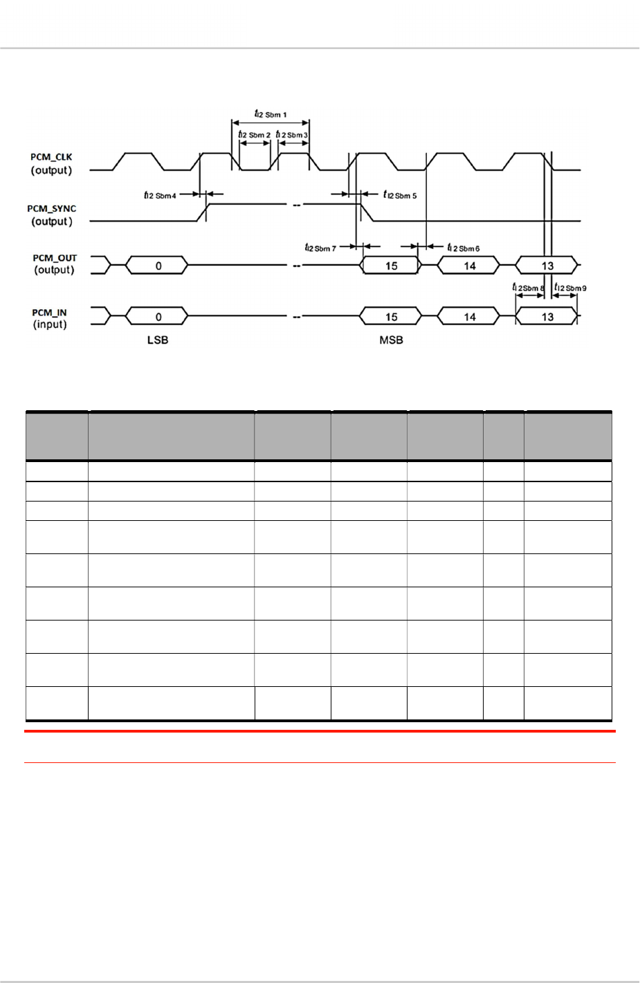
3.14.2. PCM Master Mode
Figure 9. PCM Master Mode Timing
Table 33. PCM Master Mode Parameters
Symbol Description Minimum Typical Maximum Unit Test
Condition
t
I2Sbm1
PCM_CLK clock period T-4 T - ns T = M_T
t
I2Sbm2
PCM_CLK low time T/2 – 20 T/2 - ns T = M_T
t
I2Sbm3
PCM_CLK high time T/2 – 20 T/2 - ns T = M_T
t
I2Sbm4
PCM_SYNC high begin after
clock PCM_CLK high begin -24 - 2 x t
cp
+ 12 ns t
cp
= 9.6 ns
t
I2Sbm5
PCM_SYNC high end after
PCM_CLK how end -24 - 2 x t
cp
+ 12 ns t
cp
= 9.6 ns
t
I2Sbm6
PCM_OUT invalid before
PCM_CLK low-end - - 24 ns
t
I2Sbm7
PCM_OUT valid after
PCM_CLK high begin - - t
cp
+ 12 ns t
cp
= 9.6 ns
t
I2Sbm8
PCM_IN setup time before
PCM_CLK high end t
cp
+ 50 - - ns t
cp
= 9.6 ns
t
I2Sbm9
PCM_IN hold time after
PCM_CLK low begin 12 - - Ns
Note: T corresponds to the audio sampling rate (48 kHz, 44.1 kHz, 32 kHz, 24 kHz, 22.05 kHz, 16 kHz, 12
kHz, 11.025 kHz and 8 kHz) and to the frame length (17 bit, 18bit, 32bit, 48bit or 64 bit).
41110363 Rev 4.0 October 18, 2017 37
Product Technical Specification Detailed Interface Specifications
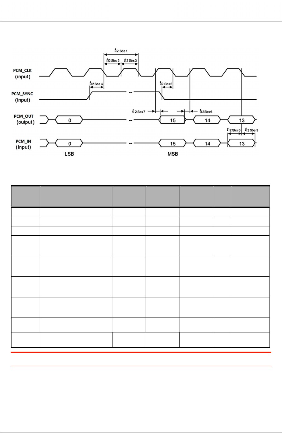
3.14.3. PCM Slave Mode
Figure 10. PCM Master Mode Timing
Table 34. PCM Slave Mode Parameters
Symbol Description Minimum Typical Maximum Unit Test
Condition
t
I2Sbs1
PCM_CLK clock period T - - n T=M_T
t
I2Sbs2
PCM_CLK low time 120 - - ns
t
I2Sbs3
PCM_CLK high time 120 - - ns
t
I2Sbs4
PCM_SYNC high begin
before PCM_CLK low begin
(latching edge of PCM_CLK)
2 x
t
cp
+ 17 - - ns
t
cp
= 9.6 ns
t
I2Sbs5
PCM_SYNC low begin
before PCM_CLK low begin
(latching edge of PCM_CLK)
2 x
t
cp
+ 17 - - ns
t
cp
= 9.6 ns
t
I2Sbs6
PCM_OUT invalid before
PCM_CLK rising edge
(shifting edge of PCM_CLK )
- - 12 ns
t
I2Sbs7
PCM_OUT valid after
PCM_CLK rising edge
(shifting edge of PCM_CLK )
- - 3 x
t
cp
+ 12 ns
t
cp
= 9.6 ns
t
I2Sbs8
PCM_IN setup time before
PCM_CLK falling edge
t
cp
+ 12 - - ns
t
cp
= 9.6 ns
t
I2Sbs9
PCM_IN hold time after
PCM_CLK falling edge 24 - - ns
Note: T corresponds to the audio sampling rate (48 kHz, 44.1 kHz, 32 kHz, 24 kHz, 22.05 kHz, 16 kHz, 12
kHz, 11.025 kHz and 8 kHz) and to the frame length (17 bit, 18bit, 32bit, 48bit or 64 bit).
41110363 Rev 4.0 October 18, 2017 38
Product Technical Specification Detailed Interface Specifications
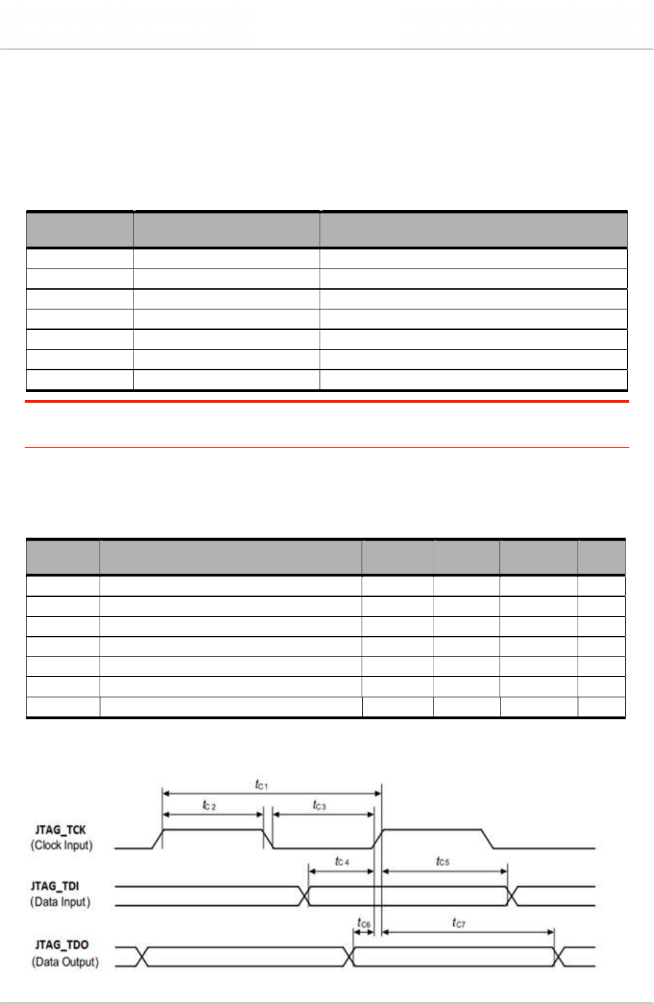
3.15. JTAG
The JTAG interface provides debug access to the core of the AirPrime HL7650 module. These JTAG
signals are accessible through solderable test points.
Refer to the following table for the pad description of the JTAG interface.
Table 35. JTAG Pad Description
Pad Number Signal Name Function
236 JTAG_RESET JTAG RESET
237 JTAG_TCK JTAG Test Clock
238 JTAG_TDO JTAG Test Data Output
239 JTAG_TMS JTAG Test Mode Select
240 JTAG_TRST JTAG Test Reset
241 JTAG_TDI JTAG Test Data Input
242 JTAG_RTCK JTAG Returned Test Clock
Note: It is recommended to provide access through Test Points to this interface the JTAG pads (for
Failure Analysis debugging). All signals listed in table above shall be outputs on the customer board
to allow JTAG debugging.
Refer to the following table for the electrical characteristics of the JTAG interface.
Table 36. JTAG Electrical Characteristics
Symbol Parameter Minimum Typical Maximum Unit
F
tck
JTAG_TCK clock period 0.038 26 78 MHz
t
c2
JTAG_TCK clock period high 12 - - ns
t
c3
JTAG_TCK clock period low 12 - - ns
t
c4
JTAG_TDI setup time to JTAG_TCK 12 - - ns
t
c5
JTAG_TDI hold time from JTAG_TCK 10 - - ns
t
c6
JTAG_TDO valid before JTAG_TCK low-end - 0 - s
t
c7
JTAG_TDO valid after JTAG_TCK high begin - 20 - ns
The following figure shows the JTAG timing waveform.
Figure 11. JTAG Timing Waveform
41110363 Rev 4.0 October 18, 2017 39
Product Technical Specification Detailed Interface Specifications
3.16. RF Interface
The RF interface of the AirPrime HL7650 module allows the transmission of RF signals. This interface
has a 50Ω nominal impedance.
Note that if the final application is a single antenna receiver (does not use the diversity antenna), it is
recommended that the diversity antenna be disabled using AT command AT+WMANTSEL. Disabling
the diversity antenna when not used:
prevents any noise in the diversity antenna input from degrading the overall sensitivity
performance of the main RF input, and
reduces the power consumption of the module.
Refer to document [2] AirPrime HL76xx AT Commands Interface Guide for more information
regarding AT+WMANTSEL.
3.16.1. RF Connection
A 50Ω (with maximum VSWR 1.1:1, and 0.5 dB loss) RF track is recommended to be connected to
standard RF connectors such as SMA, UFL, etc. for antenna connection.
Refer to the following tables for the pad description of the RF interface.
Table 37. RF Main Connection
Pad Number RF Signal Impedance VSWR Rx (max) VSWR Tx (max)
49 RF_MAIN 50Ω 1.5:1 1.5:1
Table 38. RF Diversity Connection
Pad Number RF Signal Impedance VSWR Rx (max) VSWR Tx (max)
31 RF_DIV 50Ω 1.5:1 ---
3.16.2. RF Performances
Table 39. Conducted RX Sensitivity (dBm) – UMTS Bands @ 25°C
Frequency Band Primary (Typical) Secondary (Typical)
UMTS B1
0.1% BER 12.2 kbps
-108 -111
UMTS B5 -111 -112
UMTS B8 -110 -111.5
4G RF performances are compliant with 3GPP recommendation TS 36.101.
41110363 Rev 4.0 October 18, 2017 40
Product Technical Specification Detailed Interface Specifications
Table 40. Conducted RX Sensitivity (dBm) – LTE Bands @ 25°C
Frequency Band Primary (Typical) Secondary (Typical) SIMO (Typical)
LTE B3 Full RB; BW: 20 MHz* -93 (TBC) -95.5 (TBC) -97 (TBC)
LTE B5 Full RB; BW: 10 MHz* -97 -99.5 -101
LTE B8 Full RB; BW: 10 MHz* -97 -99.5 -101
LTE B28 Full RB; BW: 20 MHz* -89 -96 -97
* Sensitivity values scale with bandwidth: x_MHz_Sensitivity = 10 MHz_Sensitivity – 10*log (10 MHz/x_MHz)
3.16.3. TX_ON Indicator (TX_ON)
The AirPrime HL7650 provides a signal, TX_ON, for TX indication. The TX_ON is a 2.3V (TBC) signal
and its status signal depends on the module’s transmitter state.
Refer to the following table for the pad description of the TX_ON signal.
Table 41. TX_ON Indicator Pad Description
Pad Number Signal Name Function I/O type Power Supply Domain
60 TX_ON TX indicator O 2.3V (TBC)
Refer to the following table for the status of the TX_ON signal depending on the embedded module’s
state.
Table 42. Burst Indicator States
Embedded Module State TX_ON
During TX burst High
No TX Low
During TX burst, there is a higher current drain from the VBATT_PA power supply which causes a
voltage drop. This voltage drop from VBATT_PA is a good indication of a high current drain situation
during TX burst.
The blinking frequency is about 217 Hz in 2G, continuous in 3G (TBC) and blinking in 4G at (TBC) Hz.
The output logic high duration, T
duration
, depends on the number of TX slots and is computed as
follows:
T duration = T advance + (0.577ms x number of TX slots) + T delay
Table 43. TX_ON Burst Characteristics
Parameter Minimum Typical Maximum
T
advance
30µs
T
delay
0µs
41110363 Rev 4.0 October 18, 2017 41
Product Technical Specification Detailed Interface Specifications
TX_ON
VBATT _PA
T
duration
T
advance
T
delay
Voltage drop
Figure 12. TX_ON State During Transmission
41110363 Rev 4.0 October 18, 2017 42
4. Mechanical Drawings
Figure 13. Mechanical Drawing
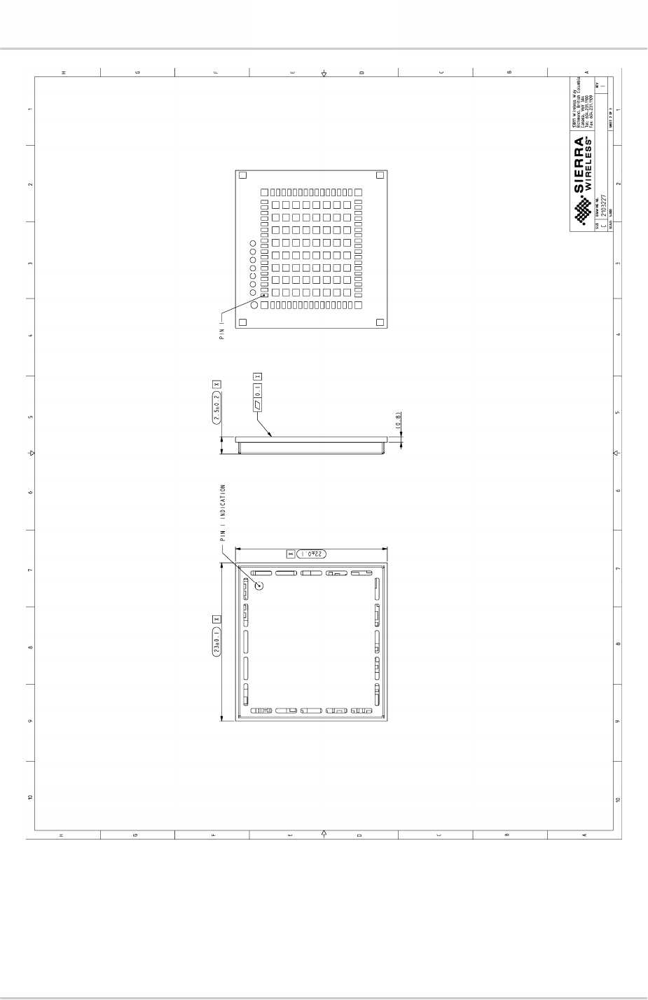
41110363 Rev 4.0 October 18, 2017 43
Product Technical Specification Mechanical Drawings
Figure 14. Dimensions Drawing
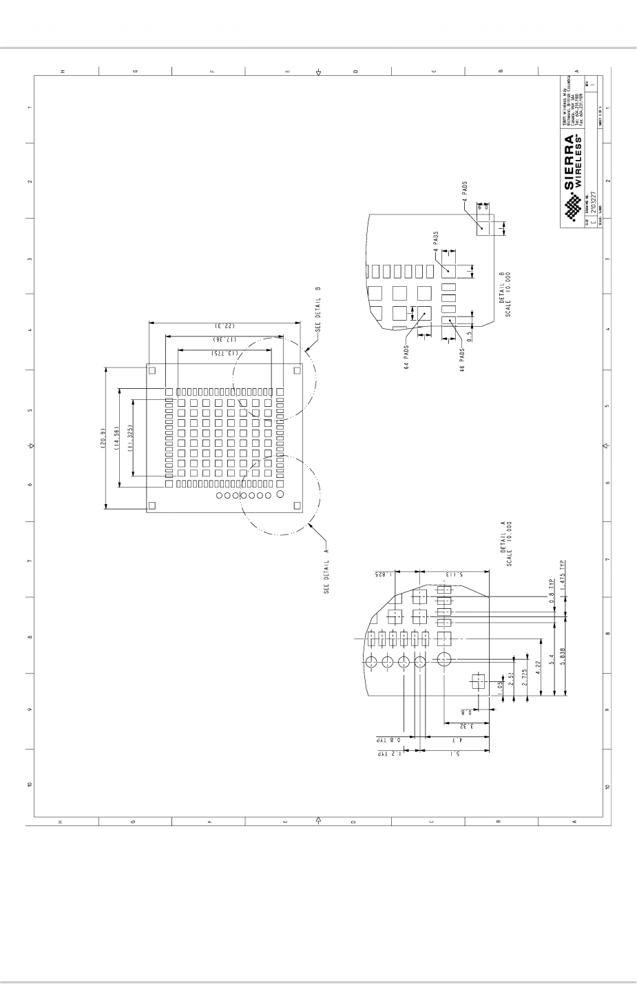
41110363 Rev 4.0 October 18, 2017 44
Product Technical Specification Mechanical Drawings
Figure 15. Footprint
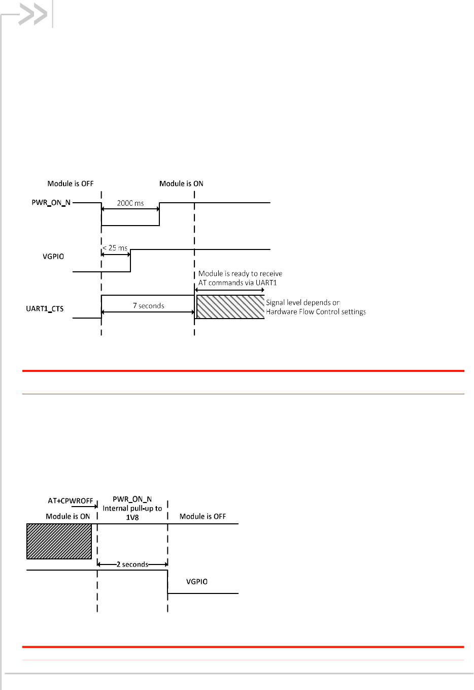
41110363 Rev 4.0 October 18, 2017 45
5. Design Guidelines
5.1. Power-Up Sequence
Apply a low-level logic to the PWR_ON_N pad (pad 59); within approximately 25ms, VGPIO will appear
to be at 1.8V. Either UART1 or the USB interface could be used to send AT commands. The AT
command interface is available in about 7 seconds after PWR_ON_N for either UART or USB.
When using UART, the AT command interface is available after the transition of UART1_CTS from high
to low level.
When using a USB connection, the HL7650 will start communicating with the host after USB
enumeration. The time when AT commands can be sent will depend on the initialization time on the
USB host.
Figure 16. PWR_ON_N Sequence with VGPIO Information
Note: As PWR_ON_N is internally pulled up with 100kΩ, an open collector or open drain transistor must be
used for ignition.
The PWR_ON_N pad has the minimum assertion time requirement of 25ms, with LOW active. Once the
valid power on trigger is detected, the PWR_ON_N pad status can be left open.
5.2. Module Switch-Off
AT command AT+CPWROFF enables the user to properly switch the AirPrime HL7650 module off.
Figure 17. Power OFF Sequence for PWR_ON_N, VGPIO
Note: PWR_ON_N is internally pulled up by 100kΩ to 1.8V.
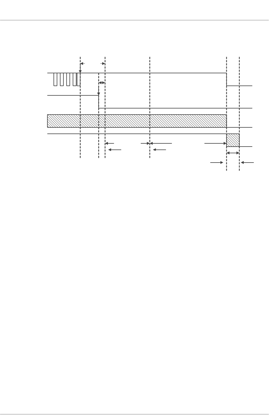
41110363 Rev 4.0 October 18, 2017 46
Product Technical Specification Design Guidelines
5.3. Hardware Fast Shut Down
The fast shutdown event can be triggered by either AT+CPWROFF=1 or a GPIO edge.
UART TX
GPIO Shutdown
Other GPIOs
VGPIO
or
Fast Detach
request
Fast Detach done
Shutdown request:
- NVMs and other processes
-GPIOs All GPIO off VGPIO off
t3 = 60 to 80 ms t4 = 180 to 1500 ms
t5 = 10 ms
t1 = 2 ms
t2 = 300 µs
IO TRIGGERED
AT+CPWROFF=1
Figure 18. Fast Shutdown Power OFF Sequence
Note that the timings for fast detach and mobile shutdown (t3 and t4 in the diagram above) are
dependent on operators and network conditions.
Starting the shutdown procedure during the boot phase should be avoided as this may cause the
shutdown to take more time.
5.4. Emergency Power OFF
If required, the module can be switched off by controlling the RESET_IN_N pad (pad 11). This must
only be used in emergency situations if the system freezes (not responding to AT commands).
To perform an emergency power off, a low-level pulse must be sent on the RESET_IN_N pad for 20ms
while the PWR_ON_N signal is inactive (high level). This action will immediately shut the HL7650
module down and the registers of the CPU and RAM memory will be reset for the next power on.
5.5. Sleep Mode Management
AT command AT+KSLEEP enables sleep mode configuration. Note that this is only used with serial link
UART1.
AT+KSLEEP=0:
The module is active when DTR signal is active (low electrical level).
When DTR is deactivated (high electrical level), the module enters sleep mode after a while.
On DTR activation (low electrical level), the module wakes up.
41110363 Rev 4.0 October 18, 2017 47
Product Technical Specification Design Guidelines
AT+KSLEEP=1:
The module determines when it enters sleep mode (when no more tasks are running).
“0x00” character on the serial link wakes the module up.
AT+KSLEEP=2: The module never enters sleep mode.
5.6. Power Supply Design
The AirPrime HL7650 module should not be supplied with voltage over 4.5V even temporarily or
however briefly.
If the system’s main board power supply unit is unstable or if the system’s main board is supplied with
over 4.5V, even in the case of transient voltage presence on the circuit, the module’s power amplifier
may be severely damaged.
To avoid such issues, add a voltage limiter to the module’s power supply lines so that VBATT and
VBATT_PA signal pads will never receive a voltage surge over 4.5V. The voltage limiter can be as
simple as a Zener diode with decoupling capacitors as shown in the diagram below.
Power Supply VBATT/VBATT _PA
D404
0.5 pF
D405
C404
1.5 mF +
+
C405
150 µF
C407
100 nF
Figure 19. Voltage Limiter Example
5.7. EMC and ESD Guidelines for USIM
Decoupling capacitors must be added according to the drawings below as close as possible to the
USIM connectors on UIMx_CLK, UIMx_RST, UIMx_VCC, UIMx_DATA and UIMx_DET signals to avoid
EMC issues and to comply with the requirements of ETSI and 3GPP standards covering the USIM
electrical interface.
A typical schematic including USIM detection is provided below.
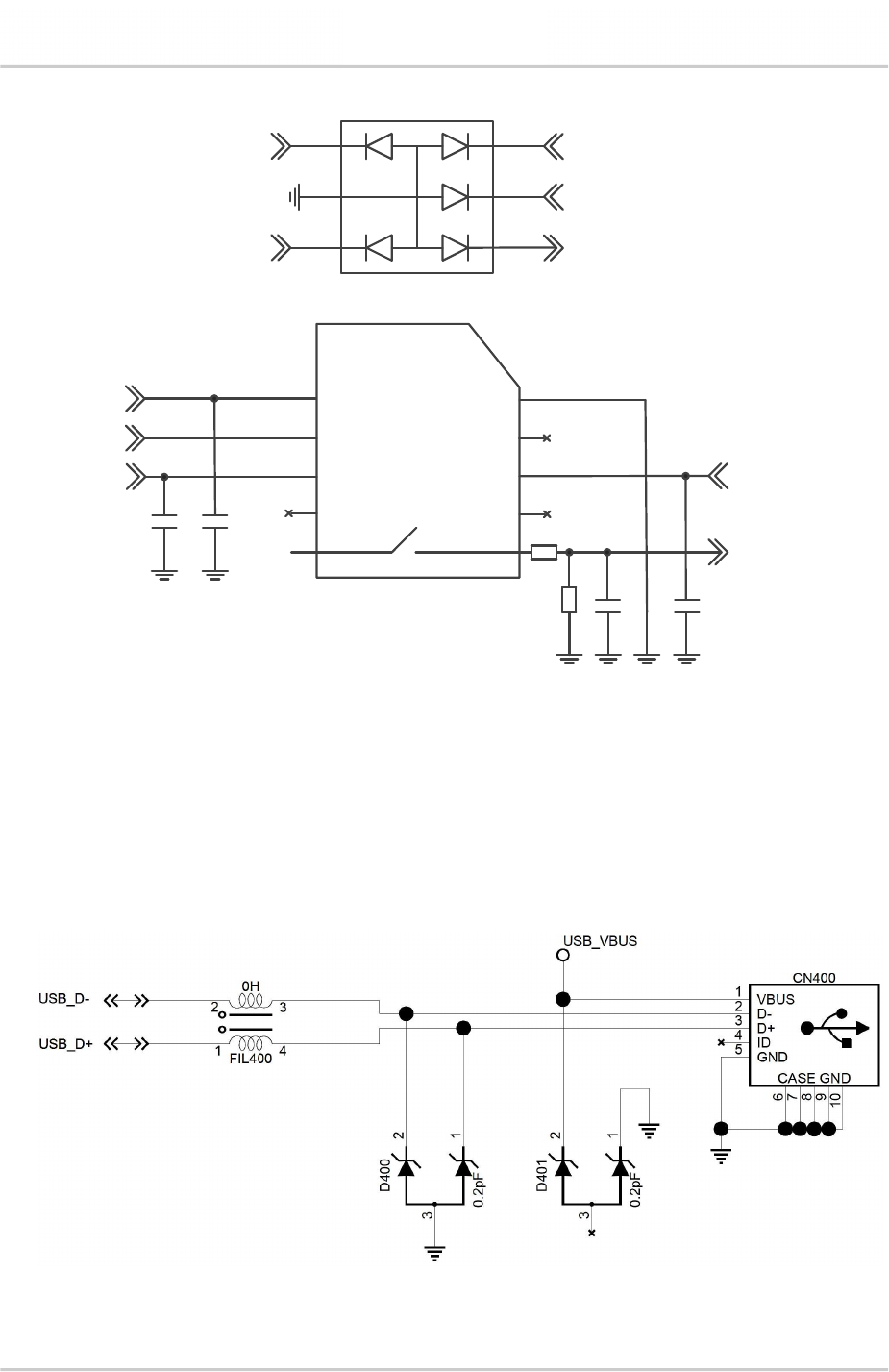
41110363 Rev 4.0 October 18, 2017 48
Product Technical Specification Design Guidelines
UIMx_VCC
UIMx_DATA
UIMx_CLK
UIMx_RESET
UIMx_DET
VGPIO
100nF
DNI
UIMx_VCC
UIMx_RESET
UIMx_CLK
1KΩ
100KΩ
DNI
1nF
1 VCC
2 RST
3 CLK
4 C4
9 SW_A SW_B 10
C8 8
I/O 7
VPP 6
GND 5
D100
12pF
CN100
UIMx_DATA
UIMx_DET
Figure 20. EMC and ESD Components Close to the USIM
Sierra Wireless recommends using diode ESDALC6V1-5P6 ESD for D100.
5.8. ESD Guidelines for USB
When the USB interface is externally accessible, it is required to have ESD protection on the
USB_VBUS, USB_D+ and USB_D- signals.
Figure 21. ESD Protection for USB
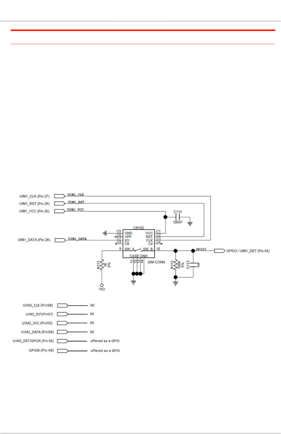
41110363 Rev 4.0 October 18, 2017 49
Product Technical Specification Design Guidelines
Note: It is not recommended to have an ESD diode with feedback path from USB_VBUS to either USB_D+
or USB_D-.
Sierra Wireless recommends using components:
90Ω DLP0NSN900HL2L EMC filter for FIL400, and
RCLAMP0503N or ESD5V3U2U-03LRH ESD diode for D400.
5.9. USIM Application
The AirPrime HL7650 supports either a single USIM design or a dual USIM configuration using DSSS
(Dual SIM Single Standby).
5.9.1. Single USIM Design
Single USIM design is supported using the following:
1 USIM slot
1 USIM connector
1 GPIO SIM detect
Figure 22. Single USIM Application (1 USIM Slot and 1 USIM Connector)
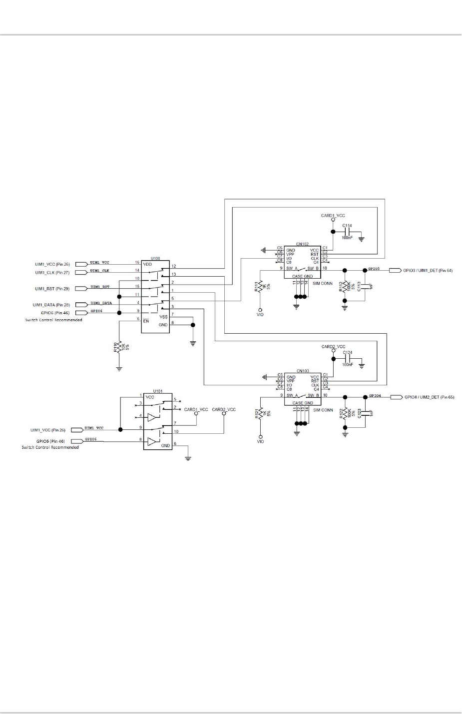
41110363 Rev 4.0 October 18, 2017 50
Product Technical Specification Design Guidelines
5.9.2. Dual SIM Single Standby Design
Dual SIM Single Standby (DSSS) with fast network switching is supported using the following:
1 USIM slot
1 or 2 external switches
2 USIM connectors
2 GPIO SIM Detect
1 GPIO switch command
Figure 23. Dual SIM Single Standby Application (1 USIM Slot and 2 USIM Connectors)
41110363 Rev 4.0 October 18, 2017 51
6. Reliability Specification
AirPrime HL7650 module is tested against the Sierra Wireless Industrial Reliability Specification defined
below.
6.1. Reliability Compliance
AirPrime HL7650 modules connected on a development kit board application are compliant with the
following requirements.
Table 44. Standards Conformity
Abbreviation Definition
IEC International Electro technical Commission
ISO International Organization for Standardization
6.2. Reliability Prediction Model
6.2.1. Life Stress Test
The following tests the AirPrime HL7650 module’s product performance.
Table 45. Life Stress Test
Designation Condition
Performance Test
PT3T & PTRT
Standard: N/A
Special conditions:
Temperature:
Class A: -30°C to +70°C
Class B: -40°C to +85°C
Rate of temperature change: ± 3°C/min
Recovery time: 3 hours
Operating conditions: Powered
Duration: 14 days
41110363 Rev 4.0 October 18, 2017 52
Product Technical Specification Reliability Specification
6.2.2. Environmental Resistance Stress Tests
The following tests the AirPrime HL7650 module’s resistance to extreme temperature.
Table 46. Environmental Resistance Stress Tests
Designation Condition
Cold Test Active
COTA
Standard: IEC 680068-2-1, Test Ad
Special conditions:
Temperature: -40°C
Temperature variation: 1°C/min
Operating conditions: Powered ON with a power cycle of 1 minute ON and
2 minutes OFF
Duration: 3 days
Resistance to Heat Test
RH
Standard: IEC 680068-2-2, Test Bb
Special conditions:
Temperature: +85°C
Temperature variation: 1°C/min
Operating conditions: Powered ON with a power cycle of 15 minutes ON
and 15 minutes OFF
Duration: 50 days
6.2.3. Corrosive Resistance Stress Tests
The following tests the AirPrime HL7650 module’s resistance to corrosive atmosphere.
Table 47. Corrosive Resistance Stress Tests
Designation Condition
Humidity Test
HUT
Standard: IEC 60068-2-3, Test Ca
Special conditions:
Temperature: +65°C
RH: 95%
Temperature variation: 3 ± 0.6°C/min
Operating conditions: Powered on, DUT is powered up for 15 minutes and
OFF for 15 minutes
Duration: 10 days
41110363 Rev 4.0 October 18, 2017 53
Product Technical Specification Reliability Specification
Designation Condition
Component Solder Wettability
CSW
Standard: JESD22 – B102, Method 1/Condition C, Solderability Test
Method
Special conditions:
Test method: Dip and Look Test with Steam preconditioning 8
h ±15min. dip for 5 +0/-0.5 seconds
Operating conditions: Un-powered
Duration: 1 day
Moist Heat Cyclic Test
MHCT
Standard: IEC 60068-2-30, Test Db
Special conditions:
Upper temperature: +40 ± 2°C
Lower temperature: +25 ± 5°C
RH:
Upper temperature: 93%
Lower temperature: 95%
Number of cycles: 21 (1 cycle/24 hours)
Temperature Variation: 3 ± 0.6°C/min
Operating conditions: Powered ON for 15 minutes during each 3 hours
ramp up and 3 hours ramp down (in middle) for every cycle
Duration: 21 days
6.2.4. Thermal Resistance Cycle Stress Tests
The following tests the AirPrime HL7650 module’s resistance to extreme temperature cycling.
Table 48. Thermal Resistance Cycle Stress Tests
Designation Condition
Thermal Shock Test
TSKT
Standard: IEC 60068-2-14, Test Na
Special conditions:
Temperature: -30°C to +80°C
Temperature Variation: less than 30s
Number of cycles: 600
Dwell Time: 10 minutes
Operating conditions: Un-powered
Duration: 9 days
Temperature Change
TCH
Standard: IEC 60068-2-14, Test Nb
Special conditions:
Temperature: -40°C to +90°C
Temperature Variation: 3 ±- 0.6°C/min
Number of cycles: 400
Dwell Time: 10 minutes
Operating conditions: Un-powered
Duration: 29 days
41110363 Rev 4.0 October 18, 2017 54
Product Technical Specification Reliability Specification
6.2.5. Mechanical Resistance Stress Tests
The following tests the AirPrime HL7650 module’s resistance to vibrations and mechanical shocks.
Table 49. Mechanical Resistance Stress Tests
Designation Condition
Sinusoidal Vibration Test
SVT
Standard: IEC 60068-2-6, Test Fc
Special conditions:
Frequency range: 16 Hz to 1000 Hz
Displacement: 0.35mm (peak-peak)
Acceleration:
5G from 16 to 62 Hz
3G from 62 to 200 Hz
1G from 200 to 1000 Hz
Sweep rate: 1 octave / cycle
Number of Sweep: 20 sweeps/axis
Sweep direction: ± X, ± Y, ± Z
Operating conditions: Un-powered
Duration: 2 days
Random Vibration Test
RVT
Standard: IEC 60068-2-64, Test Fh
Special conditions:
Frequency range: 10 Hz – 2000 Hz
Power Spectral Density in [(m/s²)²/Hz]
0.1 g2/Hz at 10Hz
0.01 g2/Hz at 250Hz
0.005 g2/Hz at 1000Hz
0.005 g2/Hz at 2000Hz
Peak factor: 3
Duration per Axis: 1 hr / axis
Operating conditions: Un-powered
Duration: 1 day
Mechanical Shock Test
MST
Standard: IEC 60068-2-27, Test Ea
Special conditions:
Shock Test 1:
Wave form: Half sine
Peak acceleration: 30g
Duration: 11ms
Number of shocks: 8
Direction: ±X, ±Y, ±Z
Shock Test 2:
Wave form: Half sine
Peak acceleration: 100g
Duration: 6ms
Number of shocks: 3
Direction: ±X, ±Y, ±Z
Operating conditions: Un-powered
Duration: 72 hours
41110363 Rev 4.0 October 18, 2017 55
Product Technical Specification Reliability Specification
6.2.6. Handling Resistance Stress Tests
The following tests the AirPrime HL7650 module’s resistance to handling malfunctions and damage.
Table 50. Handling Resistance Stress Tests
Designation Condition
ESDC Test
Standard: JESD22-A114, JESD22-A115, JESD22-C101
Special conditions:
HBM (Human Body Model): 1KV (Class 1C)
MM (Machine Model): 200V
CDM (Charged Device Model): 250V (Class II)
Operating conditions: Powered
Duration: 3 days
ESD Test
Standard: IEC 61000-4-2
Special conditions:
Contact Voltage: ±2kV, ±4kV, ±6kV
Air Voltage: ±2kV, ±4kV, ±8kV
Operating conditions: Powered
Duration: 3 days
Free Fall Test
FFT 1
Standard: IEC 60068-2-32, Test Ed
Special conditions:
Number of drops: 2 drops per unit
Height: 1m
Operating conditions: Un-powered
Duration: 6 hours
41110363 Rev 4.0 October 18, 2017 56
7. FCC Regulations
The HL7650 module has been granted modular approval for mobile applications. Integrators may use
the HL7650 module in their final products without additional FCC certification if they meet the
following conditions. Otherwise, additional FCC approvals must be obtained.
1. At least 20 cm separation distance between the antenna and the user’s body must be
maintained at all times.
2. To comply with FCC regulations limiting both maximum RF output power and human
exposure to RF radiation, the maximum antenna gain including cable loss in a mobile-only
exposure condition must not exceed:
5 dBi in LTE Band 5
3. The HL7650 module must not transmit simultaneously with other collocated radio transmitters
within a host device.
4. The RF signal must be routed on the application board using tracks with a 50Ω characteristic
impedance. Basically, the characteristic impedance depends on the dielectric, the track width
and the ground plane spacing. In order to respect this constraint, Sierra Wireless
recommends using MicroStrip or StripLine structure and computing the Tracks width with a
simulation tool (like AppCad shown in the figure below and that is available free of charge at
http://www.agilent.com).

41110363 Rev 4.0 October 18, 2017 57
Product Technical Specification FCC Regulations
If a multi-layered PCB is used, the RF path on the board must not cross any signal (digital,
analog or supply).
If necessary, use StripLine structure and route the digital line(s) "outside" the RF structure. An
example of proper routing is shown in the figure below.
Stripline and Coplanar design requires having a correct ground plane at both sides.
Consequently, it is necessary to add some vias along the RF path. It is recommended to use
Stripline design if the RF path is fairly long (more than 3cm), since MicroStrip design is not
shielded. Consequently, the RF signal (when transmitting) may interfere with neighbouring
electronics (AF amplifier, etc.). In the same way, the neighbouring electronics (micro-
controllers, etc.) may degrade the reception performances. The antenna connector is
intended to be directly connected to a 50Ω antenna and no matching is needed.
5. A label must be affixed to the outside of the end product into which the HL7650 module is
incorporated, with a statement similar to the following:
This device contains FCC ID: N7NHL7650
6. A user manual with the end product must clearly indicate the operating requirements and
conditions that must be observed to ensure compliance with current FCC RF exposure
guidelines.
The end product with an embedded HL7650 module may also need to pass the FCC Part 15
unintentional emission testing requirements and be properly authorized per FCC Part 15.
Note: If this module is intended for use in a portable device, you are responsible for separate approval to
satisfy the SAR requirements of FCC Part 2.1093.

41110363 Rev 4.0 October 18, 2017 58
8. Ordering Information
Table 51. Ordering Information
Model Name Description Part Number
HL7650 HL7650 embedded module Contact Sierra Wireless for the latest SKU
DEV-KIT HL Series Development Kit 6000620

41110363 Rev 4.0 October 18, 2017 59
9. Terms and Abbreviations
Abbreviation Definition
ADC Analog to Digital Converter
AGC Automatic Gain Control
AT Attention (prefix for modem commands)
CDMA Code Division Multiple Access
CF3 Common Flexible Form Factor
CLK Clock
CODEC Coder Decoder
CPU Central Processing Unit
DAC Digital to Analog Converter
DTR Data Terminal Ready
EGNOS European Geostationary Navigation Overlay Service
EMC Electromagnetic Compatibility
EMI Electromagnetic Interference
EN Enable
ESD Electrostatic Discharges
ETSI European Telecommunications Standards Institute
FDMA Frequency-division multiple access
GAGAN GPS aided geo augmented navigation
GLONASS Global Navigation Satellite System
GND Ground
GNSS Global Navigation Satellite System
GPIO General Purpose Input Output
GPRS General Packet Radio Service
GSM Global System for Mobile communications
Hi Z High impedance (Z)
IC Integrated Circuit
IMEI International Mobile Equipment Identification
I/O Input / Output
LED Light Emitting Diode
LNA Low Noise Amplifier
MAX Maximum
MIN Minimum
MSAS Multi-functional Satellite Augmentation System
N/A Not Applicable
PA Power Amplifier
PC Personal Computer
PCB Printed Circuit Board
PCL Power Control Level
PLL Phase Lock Loop
PWM Pulse Width Modulation
QZSS Quasi-Zenith Satellite System

41110363 Rev 4.0 October 18, 2017 60
Product Technical Specification Terms and Abbreviations
Abbreviation Definition
RF Radio Frequency
RFI Radio Frequency Interference
RMS Root Mean Square
RST Reset
RTC Real Time Clock
RX Receive
SCL Serial Clock
SDA Serial Data
SIM Subscriber Identification Module
SMD Surface Mounted Device/Design
SPI Serial Peripheral Interface
SW Software
PSRAM Pseudo Static RAM
TBC To Be Confirmed
TBD To Be Defined
TP Test Point
TX Transmit
TYP Typical
UART Universal Asynchronous Receiver-Transmitter
UICC Universal Integrated Circuit Card
USB Universal Serial Bus
UIM User Identity Module
VBATT Main Supply Voltage from Battery or DC adapter
VSWR Voltage Standing Wave Ratio
WAAS Wide Area Augmentation System