Sierra Wireless MC5728 PCA,EVDO MINI-PCI EXPRESS CARD CDMA MODEM User Manual HW Integration Guide
Sierra Wireless Inc. PCA,EVDO MINI-PCI EXPRESS CARD CDMA MODEM HW Integration Guide
Manual
Includes:
MC5725 / MC5725V
MC5727 / MC5727V
MC5728 / MC5728V
MC8775 / MC8775V
MC8780 / MC8781
MC8785V
MC8790 / MC8790V
MC8791V
2130114
Rev 1.9.1
CDMA and GSM / UMTS Mini Card
Hardware Integration Guide
Proprietary and Confidential

Preface
Rev 1.9.1 Feb.09 Proprietary and Confidential 3
In the event of a discrepancy in values between this guide and the Product Specification Document (PSD), the PSD takes precedence.
Important Notice Duetothenatureofwirelesscommunications,transmission
andreceptionofdatacanneverbeguaranteed.Datamaybe
delayed,corrupted(i.e.,haveerrors)orbetotallylost.
Althoughsignificantdelaysorlossesofdataarerarewhen
wirelessdevicessuchastheSierraWirelessmodemareusedin
anormalmannerwithawell‐constructednetwork,theSierra
Wirelessmodemshouldnotbeusedinsituationswherefailure
totransmitorreceivedatacouldresultindamageofanykind
totheuseroranyotherparty,includingbutnotlimitedto
personalinjury,death,orlossofproperty.SierraWireless
acceptsnoresponsibilityfordamagesofanykindresulting
fromdelaysorerrorsindatatransmittedorreceivedusingthe
SierraWirelessmodem,orforfailureoftheSierraWireless
modemtotransmitorreceivesuchdata.
Safety and Hazards DonotoperatetheSierraWirelessmodeminareaswhere
blastingisinprogress,whereexplosiveatmospheresmaybe
present,nearmedicalequipment,nearlifesupportequipment,
oranyequipmentwhichmaybesusceptibletoanyformof
radiointerference.Insuchareas,theSierraWirelessmodem
MUSTBEPOWEREDOFF.TheSierraWirelessmodemcan
transmitsignalsthatcouldinterferewiththisequipment.
DonotoperatetheSierraWirelessmodeminanyaircraft,
whethertheaircraftisonthegroundorinflight.Inaircraft,the
SierraWirelessmodemMUSTBEPOWEREDOFF.When
operating,theSierraWirelessmodemcantransmitsignalsthat
couldinterferewithvariousonboardsystems.
Note: Some airlines may permit the use of cellular phones while the
aircraft is on the ground and the door is open. Sierra Wireless
modems may be used at this time.
Thedriveroroperatorofanyvehicleshouldnotoperatethe
SierraWirelessmodemwhileincontrolofavehicle.Doingso
willdetractfromthedriveroroperatorʹscontrolandoperation
ofthatvehicle.Insomestatesandprovinces,operatingsuch
communicationsdeviceswhileincontrolofavehicleisan
offence.
Limitation of
Liability
Theinformationinthismanualissubjecttochangewithout
noticeanddoesnotrepresentacommitmentonthepartof
SierraWireless.SIERRAWIRELESSANDITSAFFILIATES
SPECIFICALLYDISCLAIMLIABILITYFORANYANDALL
DIRECT,INDIRECT,SPECIAL,GENERAL,INCIDENTAL,
CONSEQUENTIAL,PUNITIVEOREXEMPLARYDAMAGES
INCLUDING,BUTNOTLIMITEDTO,LOSSOFPROFITSOR

CDMA and GSM / UMTS Mini Card Hardware Integration Guide
4 Proprietary and Confidential 2130114
In the event of a discrepancy in values between this guide and the Product Specification Document (PSD), the PSD takes precedence.
REVENUEORANTICIPATEDPROFITSORREVENUE
ARISINGOUTOFTHEUSEORINABILITYTOUSEANY
SIERRAWIRELESSPRODUCT,EVENIFSIERRAWIRELESS
AND/ORITSAFFILIATESHASBEENADVISEDOFTHE
POSSIBILITYOFSUCHDAMAGESORTHEYARE
FORESEEABLEORFORCLAIMSBYANYTHIRDPARTY.
Notwithstandingtheforegoing,innoeventshallSierra
Wirelessand/oritsaffiliatesaggregateliabilityarisingunderor
inconnectionwiththeSierraWirelessproduct,regardlessof
thenumberofevents,occurrences,orclaimsgivingriseto
liability,beinexcessofthepricepaidbythepurchaserforthe
SierraWirelessproduct.
Patents Portionsofthisproductmaybecoveredbysomeorallofthe
followingUSpatents:
5,515,013 5,629,960 5,845,216 5,847,553 5,878,234
5,890,057 5,929,815 6,169,884 6,191,741 6,199,168
6,339,405 6,359,591 6,400,336 6,516,204 6,561,851
6,643,501 6,653,979 6,697,030 6,785,830 6,845,249
6,847,830 6,876,697 6,879,585 6,886,049 6,968,171
6,985,757 7,023,878 7,053,843 7,106,569 7,145,267
7,200,512 7,295,171 7,287,162 D442,170 D459,303
D599,256 D560,911
andotherpatentspending.
Thisproductincludestechnologylicensedfrom
QUALCOMM®3G.
ManufacturedorsoldbySierraWirelessoritslicenseesunder
oneormorepatentslicensedfromInterDigitalGroup.
Copyright ©2009SierraWireless.Allrightsreserved.
Trademarks AirCard®and“HeartoftheWirelessMachine®”areregistered
trademarksofSierraWireless.Watcher®isatrademarkof
SierraWireless,registeredintheEuropeanCommunity.
SierraWireless,theSierraWirelesslogo,theredwavedesign,
andthered‐tippedantennaaretrademarksofSierraWireless.
Windows®isaregisteredtrademarkofMicrosoftCorporation.
QUALCOMM®isaregisteredtrademarkofQUALCOMM
Incorporated.Usedunderlicense.
Linux®isaregisteredtrademarkofLinusTorvalds.
Othertrademarksarethepropertyoftherespectiveowners.
Preface
Rev 1.9.1 Feb.09 Proprietary and Confidential 5
In the event of a discrepancy in values between this guide and the Product Specification Document (PSD), the PSD takes precedence.
Contact
Information
Consultourwebsiteforup‐to‐dateproductdescriptions,
documentation,applicationnotes,firmwareupgrades,trouble‐
shootingtips,andpressreleases:
www.sierrawireless.com
Revision History
Sales Desk: Phone: 1-604-232-1488
Hours: 8:00 AM to 5:00 PM Pacific Time
E-mail: sales@sierrawireless.com
Post: Sierra Wireless
13811 Wireless Way
Richmond, BC
Canada V6V 3A4
Fax: 1-604-231-1109
Web: www.sierrawireless.com
Revision
number Release
date Changes
1.5 Jul 2007 •Added 8780/81 content
•Added SED description
•Fixed details about capacitance
•Added connector pin details
1.6 Unreleased Changes incorporated into v1.7.
1.7 Apr 2008 •Removed references to RUIM
(MC57xx products)
•Removed “Diversity antenna
must fold down” (“Diversity
antenna design requirements
(MC57xx / MC8780 / MC8781 /
MC8785V / MC8790 / MC8790V
/ MC8791V / MC8792V)” on
page 105).
•Removed references to
MC5720, MC8755, MC8755V,
and MC8765.
•Corrected LED characteristics
(“Faster blink” on page 64)
•Added content for MC5725,
MC5725V, and MC8785V
CDMA and GSM / UMTS Mini Card Hardware Integration Guide
6 Proprietary and Confidential 2130114
In the event of a discrepancy in values between this guide and the Product Specification Document (PSD), the PSD takes precedence.
1.8 Sep 2008 •Added content for MC8790,
MC8790V, MC8791V, and
MC8792V
1.9 Oct 2008 •Added AT command entry timing
note and Linux content to testing
chapter
•Corrected range for external pull
up resistor in Figure 5-2
1.91 Feb 2009 •Added content for MC5728 and
MC5728V (FCC)
Revision
number Release
date Changes

Rev 1.9.1 Feb.09 Proprietary and Confidential 7
In the event of a discrepancy in values between this guide and the Product Specification Document (PSD), the PSD takes precedence.
Table of Contents
Introduction . . . . . . . . . . . . . . . . . . . . . . . . . . . . . . . . . . . . . . . . . . . . . .11
The Universal Development Kit . . . . . . . . . . . . . . . . . . . . . . . . . . . . . . . . . . . . . 11
Required connectors . . . . . . . . . . . . . . . . . . . . . . . . . . . . . . . . . . . . . . . . . . . . . . 12
Guide organization . . . . . . . . . . . . . . . . . . . . . . . . . . . . . . . . . . . . . . . . . . . . . . . . 12
Related documents. . . . . . . . . . . . . . . . . . . . . . . . . . . . . . . . . . . . . . . . . . . . . . . . 13
Power Interface . . . . . . . . . . . . . . . . . . . . . . . . . . . . . . . . . . . . . . . . . . .17
Overview of operation. . . . . . . . . . . . . . . . . . . . . . . . . . . . . . . . . . . . . . . . . . . . . . 17
Power signals . . . . . . . . . . . . . . . . . . . . . . . . . . . . . . . . . . . . . . . . . . . . . . . . . 17
Electrostatic discharge (ESD) . . . . . . . . . . . . . . . . . . . . . . . . . . . . . . . . . . . 18
Module power states . . . . . . . . . . . . . . . . . . . . . . . . . . . . . . . . . . . . . . . . . . . . . . 18
Disconnected state . . . . . . . . . . . . . . . . . . . . . . . . . . . . . . . . . . . . . . . . . . . . 19
Off state . . . . . . . . . . . . . . . . . . . . . . . . . . . . . . . . . . . . . . . . . . . . . . . . . . . . . . 19
Normal state . . . . . . . . . . . . . . . . . . . . . . . . . . . . . . . . . . . . . . . . . . . . . . . . . . 19
Low power mode . . . . . . . . . . . . . . . . . . . . . . . . . . . . . . . . . . . . . . . . . . . . . . 19
Voltage monitoring state machine . . . . . . . . . . . . . . . . . . . . . . . . . . . . . . . 20
Temperature monitoring state machine . . . . . . . . . . . . . . . . . . . . . . . . . . . 22
Inrush currents . . . . . . . . . . . . . . . . . . . . . . . . . . . . . . . . . . . . . . . . . . . . . . . . . . . 24
Timing requirements . . . . . . . . . . . . . . . . . . . . . . . . . . . . . . . . . . . . . . . . . . . . . . 26
Power ramp-up . . . . . . . . . . . . . . . . . . . . . . . . . . . . . . . . . . . . . . . . . . . . . . . . 26
Power-up timing . . . . . . . . . . . . . . . . . . . . . . . . . . . . . . . . . . . . . . . . . . . . . . . 26
Transmit power wave form (GSM) . . . . . . . . . . . . . . . . . . . . . . . . . . . . . . . . . . . 26
Current consumption . . . . . . . . . . . . . . . . . . . . . . . . . . . . . . . . . . . . . . . . . . . . . . 27
Current consumption overview . . . . . . . . . . . . . . . . . . . . . . . . . . . . . . . . . . 27
Modes . . . . . . . . . . . . . . . . . . . . . . . . . . . . . . . . . . . . . . . . . . . . . . . . . . . . . . . . 34
SED (Smart Error Detection) . . . . . . . . . . . . . . . . . . . . . . . . . . . . . . . . . . . . 34
Usage models . . . . . . . . . . . . . . . . . . . . . . . . . . . . . . . . . . . . . . . . . . . . . . . . . 35

CDMA and GSM / UMTS Mini Card Hardware Integration Guide
8 Proprietary and Confidential 2130114
In the event of a discrepancy in values between this guide and the Product Specification Document (PSD), the PSD takes precedence.
RF Integration . . . . . . . . . . . . . . . . . . . . . . . . . . . . . . . . . . . . . . . . . . . 37
RF connection . . . . . . . . . . . . . . . . . . . . . . . . . . . . . . . . . . . . . . . . . . . . . . . . . . . . 39
Ground connection . . . . . . . . . . . . . . . . . . . . . . . . . . . . . . . . . . . . . . . . . . . . . . . . 39
Shielding . . . . . . . . . . . . . . . . . . . . . . . . . . . . . . . . . . . . . . . . . . . . . . . . . . . . . 40
Antenna and cabling . . . . . . . . . . . . . . . . . . . . . . . . . . . . . . . . . . . . . . . . . . . 40
Interference and sensitivity . . . . . . . . . . . . . . . . . . . . . . . . . . . . . . . . . . . . . . . . . 41
Power supply noise . . . . . . . . . . . . . . . . . . . . . . . . . . . . . . . . . . . . . . . . . . . . 41
Interference from other wireless devices . . . . . . . . . . . . . . . . . . . . . . . . . . 41
Device-generated RF . . . . . . . . . . . . . . . . . . . . . . . . . . . . . . . . . . . . . . . . . . . 42
Methods to mitigate decreased Rx performance . . . . . . . . . . . . . . . . . . . 42
Radiated sensitivity measurement. . . . . . . . . . . . . . . . . . . . . . . . . . . . . . . . . . . 43
Sierra Wireless’ sensitivity testing and desensitization investigation . . 43
OTA test chamber configuration . . . . . . . . . . . . . . . . . . . . . . . . . . . . . . . . . 43
Path loss calculation . . . . . . . . . . . . . . . . . . . . . . . . . . . . . . . . . . . . . . . . . . . 44
Positioning the DUT (Device Under Test) . . . . . . . . . . . . . . . . . . . . . . . . . 45
Sensitivity vs. frequency . . . . . . . . . . . . . . . . . . . . . . . . . . . . . . . . . . . . . . . . 45
Audio Interface . . . . . . . . . . . . . . . . . . . . . . . . . . . . . . . . . . . . . . . . . . . 51
System block diagrams . . . . . . . . . . . . . . . . . . . . . . . . . . . . . . . . . . . . . . . . . 52
Modes of operation . . . . . . . . . . . . . . . . . . . . . . . . . . . . . . . . . . . . . . . . . . . . 55
Sidetone support . . . . . . . . . . . . . . . . . . . . . . . . . . . . . . . . . . . . . . . . . . . . . . 55
Echo cancellation support . . . . . . . . . . . . . . . . . . . . . . . . . . . . . . . . . . . . . . 56
Audio signal interface . . . . . . . . . . . . . . . . . . . . . . . . . . . . . . . . . . . . . . . . . . 57
Audio function partitioning . . . . . . . . . . . . . . . . . . . . . . . . . . . . . . . . . . . . . 58
Host / Module Interfaces . . . . . . . . . . . . . . . . . . . . . . . . . . . . . . . . . . 61
Host interface pin details. . . . . . . . . . . . . . . . . . . . . . . . . . . . . . . . . . . . . . . . . . . 61
USB interface . . . . . . . . . . . . . . . . . . . . . . . . . . . . . . . . . . . . . . . . . . . . . . . . . . . . 62
USB handshaking . . . . . . . . . . . . . . . . . . . . . . . . . . . . . . . . . . . . . . . . . . . . . 62
LED output . . . . . . . . . . . . . . . . . . . . . . . . . . . . . . . . . . . . . . . . . . . . . . . . . . . 64
USIM interface . . . . . . . . . . . . . . . . . . . . . . . . . . . . . . . . . . . . . . . . . . . . . . . . 65

Table of Contents
Rev 1.9.1 Feb.09 Proprietary and Confidential 9
In the event of a discrepancy in values between this guide and the Product Specification Document (PSD), the PSD takes precedence.
USIM operation . . . . . . . . . . . . . . . . . . . . . . . . . . . . . . . . . . . . . . . . . . . . . . . 67
Extended AT commands . . . . . . . . . . . . . . . . . . . . . . . . . . . . . . . . . . . . . . . . . . . 68
Thermal Considerations . . . . . . . . . . . . . . . . . . . . . . . . . . . . . . . . . . .73
Thermal considerations . . . . . . . . . . . . . . . . . . . . . . . . . . . . . . . . . . . . . . . . . . . . 73
Design Checklist . . . . . . . . . . . . . . . . . . . . . . . . . . . . . . . . . . . . . . . . . .75
Testing . . . . . . . . . . . . . . . . . . . . . . . . . . . . . . . . . . . . . . . . . . . . . . . . . .77
AT command entry timing requirement . . . . . . . . . . . . . . . . . . . . . . . . . . . 77
Acceptance testing . . . . . . . . . . . . . . . . . . . . . . . . . . . . . . . . . . . . . . . . . . . . . . . . 77
Test requirements . . . . . . . . . . . . . . . . . . . . . . . . . . . . . . . . . . . . . . . . . . . . . 77
Test procedure . . . . . . . . . . . . . . . . . . . . . . . . . . . . . . . . . . . . . . . . . . . . . . . . 78
Certification testing . . . . . . . . . . . . . . . . . . . . . . . . . . . . . . . . . . . . . . . . . . . . . . . 78
Production testing . . . . . . . . . . . . . . . . . . . . . . . . . . . . . . . . . . . . . . . . . . . . . . . . 79
Suggested manual functional test procedure . . . . . . . . . . . . . . . . . . . . . . . . . 80
Suggested test plan procedure . . . . . . . . . . . . . . . . . . . . . . . . . . . . . . . . . . 80
Testing RF transmission path—MC57xx . . . . . . . . . . . . . . . . . . . . . . . . . . 85
Testing RF transmission path—MC87xx . . . . . . . . . . . . . . . . . . . . . . . . . . 86
Testing RF Receive path—MC57xx . . . . . . . . . . . . . . . . . . . . . . . . . . . . . . . 88
Testing RF Receive path—MC87xx . . . . . . . . . . . . . . . . . . . . . . . . . . . . . . . 90
Testing GPS Receiver—MC8775V . . . . . . . . . . . . . . . . . . . . . . . . . . . . . . . . 93
Test Audio Loop-back—MC5725V / MC5727V / MC5728V / MC8775V /
MC8785V / MC8790V / MC8791V / MC8792V . . . . . . . . . . . . . . . . . . . . . . . 94
Quality assurance testing . . . . . . . . . . . . . . . . . . . . . . . . . . . . . . . . . . . . . . . . . . 96
Suggested testing equipment. . . . . . . . . . . . . . . . . . . . . . . . . . . . . . . . . . . . . . . 97
Antenna Specification . . . . . . . . . . . . . . . . . . . . . . . . . . . . . . . . . . . .101
Required antennas . . . . . . . . . . . . . . . . . . . . . . . . . . . . . . . . . . . . . . . . . . . . . . . 101
Frequency bands . . . . . . . . . . . . . . . . . . . . . . . . . . . . . . . . . . . . . . . . . . . . . 102

CDMA and GSM / UMTS Mini Card Hardware Integration Guide
10 Proprietary and Confidential 2130114
In the event of a discrepancy in values between this guide and the Product Specification Document (PSD), the PSD takes precedence.
Antenna design . . . . . . . . . . . . . . . . . . . . . . . . . . . . . . . . . . . . . . . . . . . . . . . . . . 104
General antenna design requirements . . . . . . . . . . . . . . . . . . . . . . . . . . . 104
Main antenna design requirements . . . . . . . . . . . . . . . . . . . . . . . . . . . . . 104
Diversity antenna design requirements (MC57xx / MC8780 / MC8781 /
MC8785V / MC8790 / MC8790V / MC8791V / MC8792V) . . . . . . . . . . . . . 105
GPS antenna design requirements (MC57xx / MC8775V / MC878x) . . 105
Testing . . . . . . . . . . . . . . . . . . . . . . . . . . . . . . . . . . . . . . . . . . . . . . . . . . . . . . . . . 106
Voltage Standing Wave Ratio (VSWR) . . . . . . . . . . . . . . . . . . . . . . . . . . . 106
Efficiency . . . . . . . . . . . . . . . . . . . . . . . . . . . . . . . . . . . . . . . . . . . . . . . . . . . . 108
Antenna-to-antenna isolation . . . . . . . . . . . . . . . . . . . . . . . . . . . . . . . . . . . 108
Peak gain and radiation patterns . . . . . . . . . . . . . . . . . . . . . . . . . . . . . . . . 109
Fading correlation coefficient . . . . . . . . . . . . . . . . . . . . . . . . . . . . . . . . . . 109
Regulatory Information . . . . . . . . . . . . . . . . . . . . . . . . . . . . . . . . . . 111
Important notice . . . . . . . . . . . . . . . . . . . . . . . . . . . . . . . . . . . . . . . . . . . . . . . . . 111
Safety and hazards . . . . . . . . . . . . . . . . . . . . . . . . . . . . . . . . . . . . . . . . . . . . . . . 111
Important compliance information for North American users . . . . . . . . . . 112
EU regulatory conformity. . . . . . . . . . . . . . . . . . . . . . . . . . . . . . . . . . . . . . . . . . 113
Acronyms and Definitions . . . . . . . . . . . . . . . . . . . . . . . . . . . . . . . . 115
Index . . . . . . . . . . . . . . . . . . . . . . . . . . . . . . . . . . . . . . . . . . . . . . . . . . . 119

1
Rev 1.9.1 Feb.09 Proprietary and Confidential 11
In the event of a discrepancy in values between this guide and the Product Specification Document (PSD), the PSD takes precedence.
1: Introduction
SierraWireless’MiniCardmodulesformtheradiocomponent
fortheproductsinwhichtheyareembedded.MiniCardsare
availableforuseonCDMAandGSMnetworks,including:
Note: Throughout this
document, MC57xx and MC87xx
refer to the entire suites of
CDMA and GSM Mini Cards
respectively.
•MC5725/MC5725V/MC5727/MC5727V/MC5728/MC5728V—
OperateonCDMAnetworksusingtheCDMAIS‐95A,1X,
and1xEV‐DO(IS‐856)networkstandards,andsupport
GPS.
•MC8775 / MC8775V—operateonGSMnetworksusingthe
GSM/GPRS/EDGE/UMTS/HSDPAnetworkstandards,
andsupportStandaloneGPSfunctionality.
•MC8780 / MC8781 / MC8785V / MC8790 / MC8790V / MC8791V /
MC8792V—operateonGSMnetworksusingtheGSM/
GPRS/EDGE/UMTS/HSDPA/HSUPAnetwork
standards,andsupportStandaloneGPS,gpsOneXTRA™,
A‐GPS,selectedenhancedNavigation2.0features,andfive
NMEAsentences.
Purpose of this guide
ThisguideaddressesissuesthataffecttheintegrationofSierra
Wirelessmodulesintohostproducts,andincludesdesign
recommendationsforthehostproducts.
Note: An understanding of network technology and experience in
integrating hardware components into electronic equipment is
assumed.
The Universal Development Kit
SierraWirelessmanufacturesaUniversalDevelopmentKit
(UDK)thatfacilitatesallphasesoftheintegrationprocess.
Thiskitisahardwaredevelopmentplatformthatisdesigned
tosupportmultiplemembersofthewirelessembedded
moduleproductfamily.Itcontainsthehardwarecomponents
thataretypicallynecessaryforevaluatinganddevelopingwith
themodule,including:
•Developmentboard
•Cables
•Antennas
•Otheraccessories
ForinstructionsonsettinguptheUDK,seePCIExpressMini
CardDevKitQuickStartGuide(Document2130705).

CDMA and GSM / UMTS Mini Card Hardware Integration Guide
12 Proprietary and Confidential 2130114
In the event of a discrepancy in values between this guide and the Product Specification Document (PSD), the PSD takes precedence.
Required connectors
Note: Contact vendors before
choosing your connectors — the
numbers included here are for
reference only. Choose
connectors that are appropriate
to your design.
Whenintegratingthesemodulesintoyourhostdevice,you
needthefollowingconnectortypes:
•RFcablesthatmatewithHiroseU.FLconnectors(model
U.FL#CL331‐0471‐0‐10).Modulesincludeoneortwo
connectorjacksdependingonindividualmodulesupport
fordiversityorGPSfunctionality.
•Industry‐standardmatingconnectorfor52‐pinEDGE—
somemanufacturersincludeTyco,Foxconn,andMolex.For
example,theconnectorusedontheMiniCardDevKit
boardisaMolex67910‐0001.
•Industry‐standardUSIMconnector(MC87xxonly)—the
actualconnectoryouusedependsonhowyourdevice
exposestheUSIMsocket.Forexample,theUSIMconnector
usedontheMiniCardDevKitboardisanITTCCM03‐
3518.
Guide organization
Thisguideincludesthefollowingsections:
1. Introduction(thissection)
2. Power Interface(p.17)
Describespowercontrolsignalsusedbythemoduleand
discussesdesignissuesrelatedtopowersupply
integration.
3. RF Integration(p.37)
Describesantennaconnectionmethodsandgroundingissues,
RFinterferenceanddesenseissues.
4. Audio Interface(p.51)
Describessupportedaudiomodesandrelateddetails.
5. Host / Module Interfaces(p.61)
DescribestheUSBinterfaceforhost/modulecommunication,
andtheUSIMinterfaceforhost/moduleintegration.
6. Thermal Considerations(p.73)
Describesthermalcharacteristicsofthemoduleandprovides
suggestionsfortestingandaddressingthermalissues.
7. Design Checklist(p.75)
Summarizesdesignconsiderationsforintegrationof
MiniCardsinyourhostdevices.
8. Testing(p.77)
Describessuggestedacceptance,certification,production,and
qualityassurancetests.
9. Antenna Specification(p.101)
Describesantennarequirementsandtestingdetails.

Introduction
Rev 1.9.1 Feb.09 Proprietary and Confidential 13
In the event of a discrepancy in values between this guide and the Product Specification Document (PSD), the PSD takes precedence.
10. Regulatory Information(p.111)
Describesregulatoryapprovalsandregulatoryinformation
requirements.
11. Acronyms and Definitions(p.115)
Listsacronymsanddefinitionsusedthroughoutthisguide.
12. Index(p.119)
Note: The term "host" always refers to the host device.
Related documents
Thisguidedealsspecificallywithhardwareintegrationissues
thatareuniquetotheMC57xxandMC87xxmodules.
Table1‐1listsotherdocumentsreferencedinthisguide.
Table 1-1: Related documentation
Document title Description
AT Command Set for User
Equipment (UE) (Release 6) Standard AT commands for GSM / UMTS devices.
Download this document (3GPP TS 27.007) from
www.3gpp.org.
CDMA 1X Standard Technical requirements for CDMA systems, including
details on sleep cycle index (SCI) values.
Order this document, CDMA 2000 Series Release A
(2000) (document # TIA/EIA/IS-2000 Series, Release A)
from www.tiaonline.org.
CDMA CnS Reference
(Document 2130754) CnS (Control and Status) messages that are supported by
the MC5725 / MC5725V
CDMA AT Command Reference
(Document 2130620) Proprietary, basic AT commands for the MC5725 /
MC5725V / MC5727 / MC5727V / MC5728 / MC5728V.
For MC87xx-specific commands, see UMTS Modems
Supported AT Command Reference (Document 2130617).
CDMA Extended AT Command
Reference (Document
2130621)
Proprietary AT commands for the MC5725 / MC5725V /
MC5727 / MC5727V / MC5728 / MC5728V. For MC87xx-
specific commands, see MC87xx Modem Extended AT
Command Reference (Document 2130616).
FCC Regulations - Part 15 -
Radio Frequency Devices This section of the FCC Code of Federal Regulations, Title
47 deals with radio frequency devices, including shielding
requirements for embedded modules.
Download this regulation from http://wireless.fcc.gov.

CDMA and GSM / UMTS Mini Card Hardware Integration Guide
14 Proprietary and Confidential 2130114
In the event of a discrepancy in values between this guide and the Product Specification Document (PSD), the PSD takes precedence.
IEC-61000-4-2 level 3 Techniques for testing and measuring electrostatic
discharge (ESD) immunity.
Order this document from www.iec.ch.
MC5725 Mini Card Product
Specification (Document
2130663)
Features, mechanical and electrical specifications, and
standards compliance of the MC5725.
MC5725V Mini Card Product
Specification (Document
2130671)
Features, mechanical and electrical specifications, and
standards compliance of the MC5725V.
MC5727 Mini Card Product
Specification (Document
2130958)
Features, mechanical and electrical specifications, and
standards compliance of the MC5727.
MC5727V Mini Card Product
Specification (Document
2131023)
Features, mechanical and electrical specifications, and
standards compliance of the MC5727V.
MC5728V Mini Card Product
Specification (Document
2111350)
Features, mechanical and electrical specifications, and
standards compliance of the MC5728V.
MC8775 PCI Express Mini Card
Product Specification
(Document 2130697)
Features, mechanical and electrical specifications, and
standards compliance of the MC8775.
MC8775V with Audio PCI
Express Mini Card Product
Specification (Document
2130700)
Features, mechanical and electrical specifications, and
standards compliance of the MC8775V.
MC8780 / MC8781 PCI Express
Mini Card Product
Specification (Document
2130782)
Features, mechanical and electrical specifications, and
standards compliance of the MC8780 / MC8781.
MC8785V PCI Express Mini
Card Product Specification
(Document 2130932)
Features, mechanical and electrical specifications, and
standards compliance of the MC8785V.
MC8790 PCI Express Mini Card
Product Specification
(Document 2111279)
Features, mechanical and electrical specifications, and
standards compliance of the MC8790.
MC8790V PCI Express Mini
Card Product Specification
(Document 2111280)
Features, mechanical and electrical specifications, and
standards compliance of the MC8790V.
MC8791V PCI Express Mini
Card Product Specification
(Document 2131032)
Features, mechanical and electrical specifications, and
standards compliance of the MC8791V.
Table 1-1: Related documentation (Continued)
Document title Description

Introduction
Rev 1.9.1 Feb.09 Proprietary and Confidential 15
In the event of a discrepancy in values between this guide and the Product Specification Document (PSD), the PSD takes precedence.
MC8792V PCI Express Mini
Card Product Specification
(Document 2131033)
Features, mechanical and electrical specifications, and
standards compliance of the MC8792V.
MC87XX Modem CnS
Reference (Document
2130602)
CnS (Control and Status) messages supported by the
MC87xx series of modems.
MC87xx Modem CnS Reference
(Voice) (Document 2130817) Voice-related CnS (Control and Status) messages
supported by the MC8775V, MC8785V,
MC8790V,MC8791V, and MC8792V.
UMTS Modems Supported AT
Command Reference
(Document 2130617)
Proprietary, basic AT commands for the MC87xx. For
MC57xx-specific commands, see the CDMA AT
Command Reference (Document 2130620).
MC87xx Modem Extended AT
Command Reference
(Document 2130616)
Proprietary AT commands for the MC87xx. For MC57xx-
specific commands, see the CDMA Extended AT
Command Reference (Document 2130621).
Mobile Station (MS)
Conformance Specification;
Part 4: Subscriber Interface
Module
SIM testing methods.
Download this document (3GPP TS 11.10-4) from
www.3gpp.org.
PCI Express Mini Card Dev Kit
Quick Start Guide (Document
2130705)
Setup and configuration of modules.
PCI Express Mini Card
Electromechanical
Specification Revision 1.1
Download this document from www.pcisig.com.
Universal Serial Bus
Specification, Rev 2.0 Download this specification from www.usb.org.
Table 1-1: Related documentation (Continued)
Document title Description

CDMA and GSM / UMTS Mini Card Hardware Integration Guide
16 Proprietary and Confidential 2130114
In the event of a discrepancy in values between this guide and the Product Specification Document (PSD), the PSD takes precedence.

2
Rev 1.9.1 Feb.09 Proprietary and Confidential 17
In the event of a discrepancy in values between this guide and the Product Specification Document (PSD), the PSD takes precedence.
2: Power Interface
Overview of operation
Note: This chapter contains information for CDMA (MC57xx) and
GSM (MC87xx) modules.
Information that is unique to specific module types is clearly
identified.
Themoduleisdesignedtousea3.3V(nominal)powersupply,
providedbythehost.Itisthehost’sresponsibilitytoprovide
safeandcontinuouspowertothemoduleatalltimes;the
moduledoesNOThaveanindependentpowersupply,or
protectioncircuitstoguardagainstelectricalissues.
Thehostcontrolsthemodule’spowerstateusingthe
W_Disable#signalasshowninFigure2‐1.Thesignalisdriven
lowbythehosttopoweroffthemodem,orleftfloating(high
impedance)topoweronthemodem.Themodulealso
monitorsitssupplyvoltageandrequestsshutdownifthe
supplyisinsufficient(seeVoltage monitoring state machine,
page20).
Figure 2-1: Recommended W_Disable# connection (open
drain circuit)
Power signals
Themodulemustbeconnectedtoa3.3Vpowersupply(as
describedinPCIExpressMiniCardElectromechanicalSpecifi‐
cationRevision1.1).
TheMC87xxhasmorepowerpinsthantheMC57xxdueto
higherpeakcurrentrequirementsforGSMdevices.
Fordetailedpinoutandvoltage/currentrequirementsofthese
modules,seetheProductSpecificationDocumentforyour
MiniCard.
Control
R
W_Disable#
1
2
3
Q

CDMA and GSM / UMTS Mini Card Hardware Integration Guide
18 Proprietary and Confidential 2130114
In the event of a discrepancy in values between this guide and the Product Specification Document (PSD), the PSD takes precedence.
Note: The Product Specification Document’s pin connection table
describes the internal structure of the module. For example, a Mini
Card standard-compliant host platform provides +3.3Vaux on pin 24,
but this pin is not connected internally on the MC8775V. Thus, the pin
is flagged as ‘No connect’.
Electrostatic discharge (ESD)
Youareresponsibleforensuringthatthehosthasadequate
ESDprotectionondigitalcircuitsandantennaports:
•(Operational)RFport(antennalaunchandRFconnector):
IEC‐61000‐4‐2—Level(ElectrostaticDischargeImmunityTest)
•(Non‐operational)Hostconnectorinterface:
JESD22‐A114‐B+/‐1kVHumanBodyModeland
JESD22‐C101+/‐125VChargedDeviceModel
•MC5728/MC5728Vonly:(Non‐operational)Hostconnector
interface:
JESD22‐A114‐B+/‐200VHumanBodyModeland
JESD22‐C101+/‐250VChargedDeviceModel
MC5728/MC5728VhasplaceholdersforadditionalESD
devices,forcaseswherethedevicemust,percustomer
requirements,meetthehigherHumanBodyModel(+/‐1kV)
ESDrating.
Specificrecommendationsareprovidedwhereneededinthis
guide,however,thelevelofprotectionrequireddependson
yourapplication.
Note: ESD protection is highly recommended for the USIM connector
at the point where the contacts are exposed, and for any other signals
from the host interface that would be subjected to ESD by the user of
the product.
Module power states
Note: The module unit defaults
to the Normal state when
VCC3.3 is first applied in the
absence of W_Disable# control.
Themodulehasfourpowerstates:
•Disconnected
Nopowertothemodule.
•Off
Powertothemodule,butthemoduleispoweredoff.
•Normal
Themoduleisactive.Severalmodesarepossible(Receive,
Transmit,Sleep,Shutdown).

Power Interface
Rev 1.9.1 Feb.09 Proprietary and Confidential 19
In the event of a discrepancy in values between this guide and the Product Specification Document (PSD), the PSD takes precedence.
•Low power (“airplane mode”)
Themoduleisactive,butRFisdisabled.
Statemachinesareimplementedinthemoduletomonitorthe
powersupplyandoperatingtemperature.
Disconnected state
Note: The difference between
the Disconnected and Off states
is that, in the Off state, the
module is still connected to the
power source and draws minimal
current.
Thisstateoccurswhenthereisnopowertothemodule—the
hostpowersourceisdisconnectedfromthemoduleandall
voltagesassociatedwiththemoduleareat0V.
Whetherthehostdeviceisalsopoweredoffdependsonthe
powerraildesign.Iftheconnectionbetweenthepowerrail
andthemoduleiscontrolledbythehost,thehostcanstay
poweredonandcutthepowertoputthemodemintothe
disconnectedstate.Ifthepowerrailissharedbetweenthehost
deviceandthemodule,thehostispoweredoffwhenthe
moduleispoweredoff.
Off state
Note: The module enters the Off
state if W_Disable# is driven low
and power (Vcc) is applied to the
module, or if the module is in a
powered state and W_Disable#
is driven low for a module-
dependent minimum period. See
State change: Power off / on on
page 23 for details.
Inthisstate,thehostispoweredupandthemoduleis
powereddown(butstillconnectedtothepowersource).
Thehostkeepsthemodulepoweredoffbydrivingthe
W_Disable#signallow.Inthisstate,themoduledrawsminimal
current.
Normal state
Note: This is the default state
when VCC3.3 is first applied in
the absence of W_Disable#
control.
Thisistheactivestateofthemodule.Inthisstate:
•Themoduleisfullypowered.
•Themoduleiscapableofplacing/receivingcallsorestab‐
lishingdataconnectionsonthewirelessnetwork.
•TheUSBinterfaceisfullyactive.
Low power mode
Inthisstate,RF(bothRxandTx)isdisabledinthemodule,but
theUSBinterfaceisstillactive.Thislowpowermode
(ʺairplanemodeʺ)iscontrolledbysoftwarecommands
throughthehostinterface.

CDMA and GSM / UMTS Mini Card Hardware Integration Guide
20 Proprietary and Confidential 2130114
In the event of a discrepancy in values between this guide and the Product Specification Document (PSD), the PSD takes precedence.
Forinstructionsonusingthecommands,refertoATCommand
SetforUserEquipment(UE)(Release6)(+CFUN=0command),
CDMACnSReference(Document2130754)
(CNS_RADIO_POWER[0x1075]command),orMC87XX
ModemCnSReference(Document2130602)(DisableModem
command).
Voltage monitoring state machine
ThemodulehasastatemachinetomonitortheVCC3.3
(3.0V‐3.6V)supply(Figure2‐2).
Figure 2-2: Voltage monitoring state machine
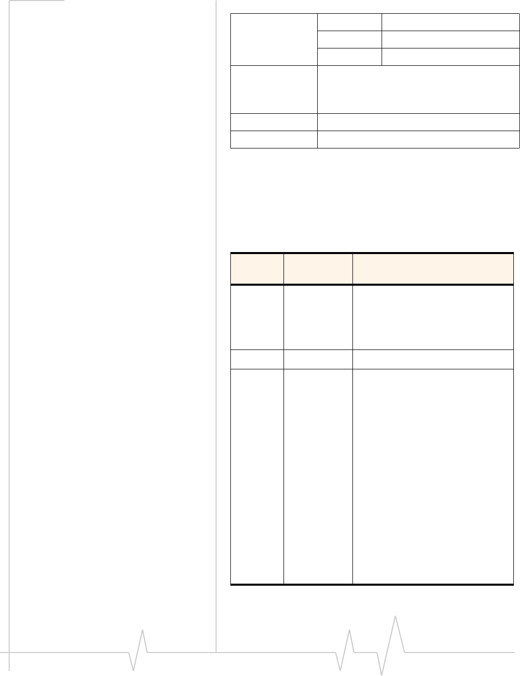
Table 2-1: Voltage trigger levels
Condition Voltage (V)
MC57xx MC8775/75V
MC8780/81 MC8785V
MC8790/90V
MC8791V/92V
VOLT_HI_CRIT 3.6 3.6 3.6
VOLT_HI_NORM 3.5 3.5 3.5
VOLT_LO_NORM 3.1 3.1 3.1
VOLT_LO_WARN 3.0 3.0 3.05
VOLT_LO_CRIT 2.9 2.9 3.00
Normal
Low Supply Voltage
Critical
(Low power mode)
Low Supply Voltage
Warning
High Supply Voltage
Critical
(Low power mode)
current_vcc > VOLT_LO_NORM
current_vcc < VOLT_LO_WARN
current_vcc > VOLT_LO_NORM
Host asserts
W_Disable#
Host asserts
W_Disable#
current_vcc
< VOLT_LO_CRIT
current_vcc > VOLT_HI_CRIT
current_vcc < VOLT_HI_NORM
Power off.
Handled by
Power State
state machine.

Power Interface
Rev 1.9.1 Feb.09 Proprietary and Confidential 21
In the event of a discrepancy in values between this guide and the Product Specification Document (PSD), the PSD takes precedence.
State change: Normal mode to Low Power mode
Thisstatechangecausesthemoduletoswitchtolowpower
mode,suspendingRFactivity.Itoccurswhenthemodule’s
supplyvoltageexceedsthelimitsdescribedinTable2‐1
(VOLT_HI_CRITandVOLT_LO_CRIT).
Whenthisstatechangeoccurs,theCnSnotification
CNS_RADIO_POWERisissued,ifenabled.Foradetailed
descriptionofthisnotification,seeCDMACnSReference
(Document2130754)orMC87XXModemCnSReference
(Document2130602).
State change: Low Power mode to Normal mode
Thisstatechangecausesthemoduletoswitchtonormalmode,
resumingRFactivity.Itoccurswhenthemodule’ssupply
voltagereturnsfromcriticaltonormallimitsasdescribedin
Table2‐1(VOLT_HI_NORMandVOLT_LO_NORM).
Whenthisstatechangeoccurs,theCnSnotification
CNS_RADIO_POWERisissued,ifenabled.Foradetailed
descriptionofthisnotification,seeCDMACnSReference
(Document2130754)orMC87XXModemCnSReference
(Document2130602).
Note: The module is still
connected to the power source
in this state, drawing minimal
power.
State change: Power off / on
Themodulebeginsashutdownsequenceandpowersoffifit
hasbeeninapowered‐onstateformorethan10.5secondsand
thehostdevicedrivestheW_Disable#signallowfor:
•≥50ms(MC8775/MC8775V)
•≥500ms(MC5725/MC5725V/MC5727/MC5727V/
MC5728/MC5728V/MC8780/MC8781/MC8785V/
MC8790/MC8790V/MC8791V/MC8792V)
Note: The module ignores changes in the W_Disable# line for the first
10.5 seconds after it enters a powered-on state.
Themodulepowersonwhenthehostdeviceleavesthe
W_Disable#signalfloating(highimpedance)asshownin
Figure2‐1onpage17.
Figure2‐2onpage20showsthetransitionfrom‘LowSupply
VoltageCritical’or‘HighSupplyVoltageCritical’to‘Power
off’:
1. Themoduleenterslowpowermodebecauseitdetectsthat
thesupplyvoltageleveliscriticallylow(VOLT_LO_CRIT)
orcriticallyhigh(VOLT_HI_CRIT).
2. ThemodulesendsaCnSnotification(ReturnRadio
Voltage—0x0009)tothehostindicatingthatitisnowin
lowpowermode.
CDMA and GSM / UMTS Mini Card Hardware Integration Guide
22 Proprietary and Confidential 2130114
In the event of a discrepancy in values between this guide and the Product Specification Document (PSD), the PSD takes precedence.
3. Thehosthastheoption,atthispoint,ofdrivingW_Disable#
low(forcingthemoduletopoweroff)topreventdamage
totheunit.
Temperature monitoring state machine
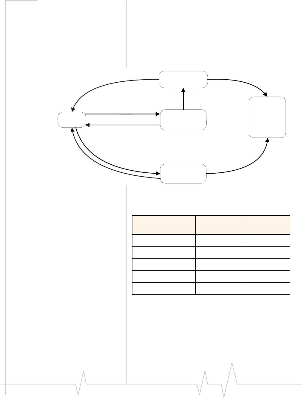
Themodulehasastatemachinetomonitorthemodule’s
temperature(Figure2‐3).
Figure 2-3: Temperature monitoring state machine
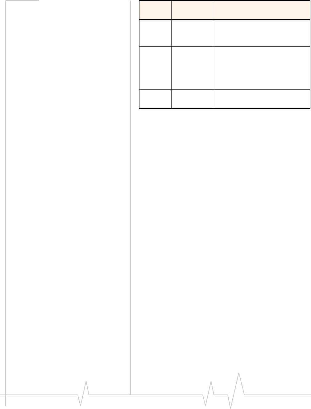
Table 2-2: Temperature trigger levels1
Condition MC57xx
Temp (°C) MC87xx
Temp (°C)
TEMP_LO_CRIT -30 -25
TEMP_NORM_LO -20 -15
TEMP_HI_NORM 85 85
TEMP_HI_WARN 95 95
TEMP_HI_CRIT 108 108
1Module-reported temperatures at the printed circuit board.
Temperature decreases from 10°C–18°C between the PCB
and the module shield, and a further 10°C–18°C between the
shield and host environment (ambient), depending on the effi-
ciency of heat-dissipation in the host device.
Normal
mode
High Temperature
Critical
(Low power mode)
High Temperature
Warning
Low Temperature
Critical
(Low power mode)
current_temp <= TEMP_HI_NORM
current_temp > TEMP_HI_WARN
current_temp < TEMP_HI_NORM
Host asserts
W_Disable#
Host asserts
W_Disable#
current_temp
> TEMP_HI_CRIT
current_temp < TEMP_LO_CRIT
current_temp > TEMP_NORM_LO
Power off.
Handled by
Power State
state machine.

Power Interface
Rev 1.9.1 Feb.09 Proprietary and Confidential 23
In the event of a discrepancy in values between this guide and the Product Specification Document (PSD), the PSD takes precedence.
State change: Normal mode to Low Power mode
Thisstatechangecausesthemoduletoswitchtolowpower
mode,suspendingRFactivity.Itoccurswhenthemodule
temperatureexceedsthelimitsdescribedinTable2‐2
(TEMP_HI_CRITandTEMP_LO_CRIT).
Whenthisstatechangeoccurs,theCnSnotification
CNS_RADIO_POWERisissued,ifenabled.Foradetailed
descriptionofthisnotification,seeCDMACnSReference
(Document2130754)orMC87XXModemCnSReference
(Document2130602).Aswell,theMC57xxissuestheCnSnotifi‐
cationModemTooHot[0x4500]ifithastodropacallwhen
shiftingtolowpowermode.
State change: Low Power mode to Normal mode
Thisstatechangecausesthemoduletoswitchtonormalmode,
resumingRFactivity.Itoccurswhenthemoduletemperature
returnsfromcriticaltonormallimitsasdescribedinTable2‐2
(TEMP_HI_NORMandTEMP_LO_NORM).
Whenthisstatechangeoccurs,theCnSnotification
CNS_RADIO_POWERisissued,ifenabled.Foradetailed
descriptionofthisnotification,seeCDMACnSReference
(Document2130754)orMC87XXModemCnSReference
(Document2130602).
State change: Power off / on
Themodulebeginsashutdownsequenceandpowersoffifit
hasbeeninapowered‐onstateformorethan10.5secondsand
thehostdevicedrivestheW_Disable#signallowfor:
•≥50ms(MC8775/MC8775V)
•≥500ms(MC5725/MC5725V/MC5727/MC5727V/
MC5728/MC5728V/MC8780/MC8781/MC8785V/
MC8790/MC8790V/MC8791V/MC8792V)
Note: The module ignores changes in the W_Disable# line for the first
10.5 seconds after it enters a powered-on state.
Themodulepowersonwhenthehostdeviceleavesthe
W_Disable#signalfloating(highimpedance)asshownin
Figure2‐1onpage17.
Figure2‐3showsthetransitionfrom‘LowTemperature
Critical’or‘HighTemperatureCritical’to‘Poweroff’.
1. Themoduleenterslowpowermodebecauseitdetectsthat
theoperatingtemperatureiscriticallylow
(TEMP_LO_CRIT)orcriticallyhigh(TEMP_HI_CRIT).
CDMA and GSM / UMTS Mini Card Hardware Integration Guide
24 Proprietary and Confidential 2130114
In the event of a discrepancy in values between this guide and the Product Specification Document (PSD), the PSD takes precedence.
2. ThemodulesendsaCnSnotification(ReturnRadio
Temperature—0x0008)tothehostindicatingthatitisnow
inlowpowermode.
3. Thehosthastheoption,atthispoint,ofdrivingW_Disable#
low(forcingthemoduletopoweroff)topreventdamage
totheunit.
Note: (MC57xx only) If the ambient temperature of the module
exceeds 60 °C, the RF level is automatically lowered for max power
transmission.
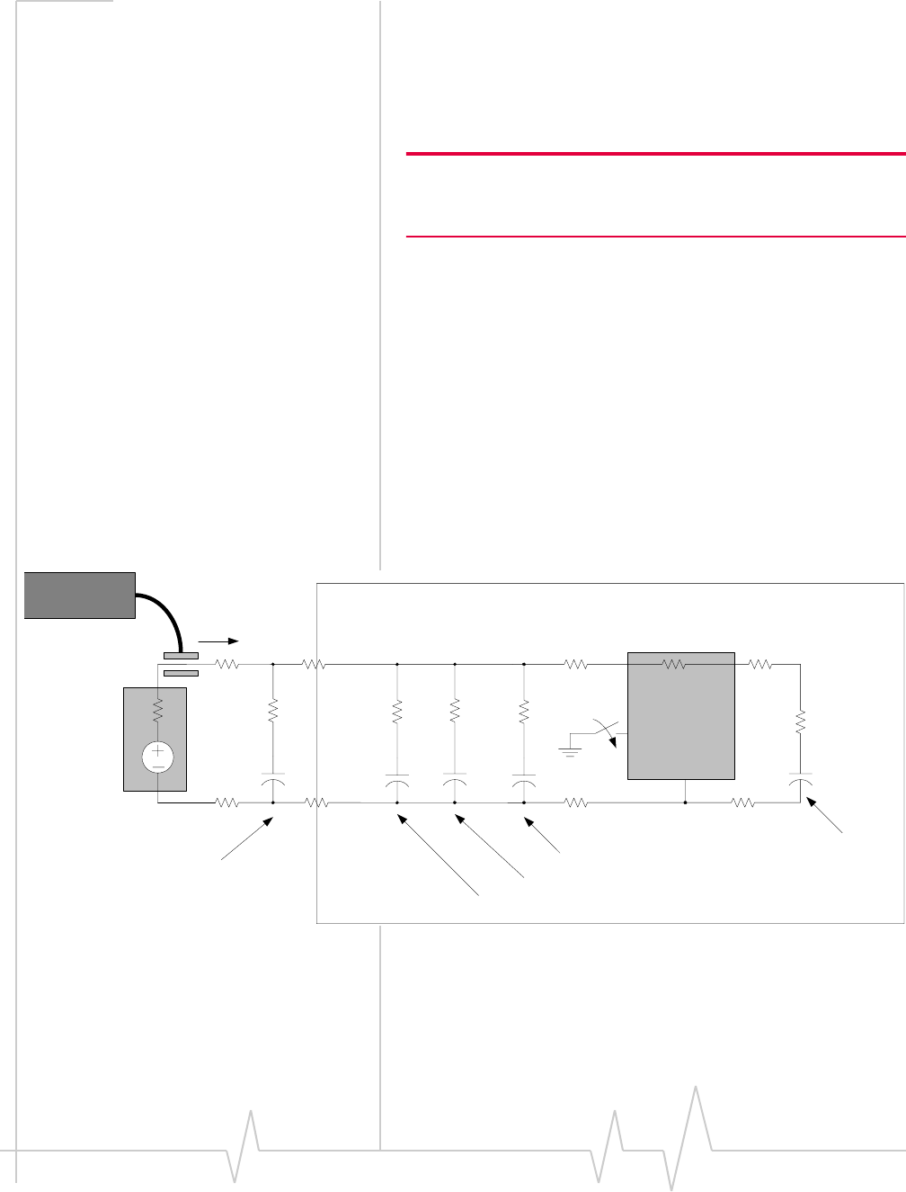
Inrush currents
Twopowereventscancauselargeinrushcurrentsfromthe
hostsupplytothemoduleonthepowerpins:
•Applicationofthehost’spowersupply
•HostleavesW_Disable#floating(highimpedance)topower
upthemodule(asshowninFigure2‐1onpage17).
Figure2‐4andFigure2‐5showtheinrushmodelsforthe
MC57xxandMC87xx.Applicationofthehost’spowersupply
typicallyoccurswhentheswitchisopen;W_Disable#isleft
floating(highimpedance)whentheswitchisclosed.
Figure 2-4: Inrush model - MC57xx
REG
PWR (1,2,3,4,5)
ON/OFF
(18)
Current
+3.3VDC
Power source
250m
LDO pass
element
1 ohm typ
ESR
80m
8.5m 2.8m 1.7m 2.2m
1uF
ESR
20m
ESR
20m
38m
Cin
2x 1uF
10m
32m
Current Probe MC57xx
Regulator input capacitor
Regulator
output
capacitor
ESR +
trace Z
60m
RF Cap
4.7uF
EM board decoupling cap
Recommended host power rail
capacitance = 470 µF - 1000 µF
Cin
2x 1uF
ESR +
trace Z
40m
EM board decoupling cap
15m
Power Interface
Rev 1.9.1 Feb.09 Proprietary and Confidential 25
In the event of a discrepancy in values between this guide and the Product Specification Document (PSD), the PSD takes precedence.
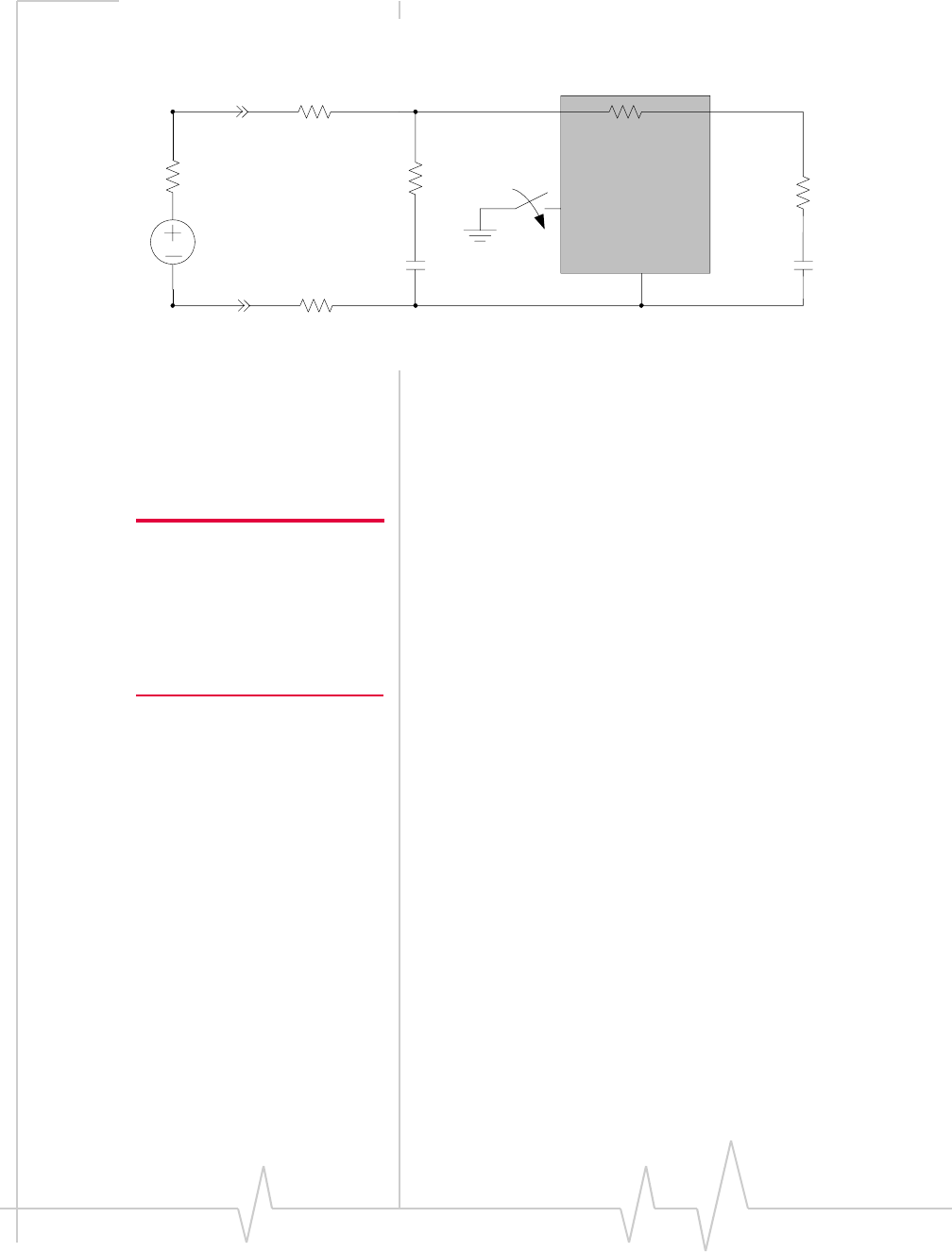
Figure 2-5: Inrush model - MC87xx
Inrush current via application of host power supply
Thiseventoccurswhenthehost’ssupplyisenabled,charging
theinputcapacitorsontheMiniCardpowerrail.Theswitch
showninFigure2‐4andFigure2‐5isopen(typically)when
thiseventoccurs.
Note: In some circumstances,
depending on temperature and
the components in use, two or
more regulators may switch on
at the same time. The host
power system must be designed
to handle this possibility.
Tolimittheinrushcurrentandstabilizethesupplyofpowerto
themodule,sufficientcapacitancemustbeaddedtothehost
powerrail.Therecommendedcapacitancerangeis
470μF‐1000μF.
Peakcurrent(IPEAK)iscalculatedusing:
Inrush current via floating W_Disable#
Thesecondeventtypeoccurswhenthehostleavesthe
W_Disable#signalfloating(highimpedance)topowerupthe
module.TheswitchshowninFigure2‐4andFigure2‐5is
closedwhenthiseventoccurs.Thisenablesthepower
managementsystemofthemodule,chargingseveralinternal
regulatoroutputcapacitors.
WhenW_Disable#isleftfloating(highimpedance),thepeak
currentislessthan500mA(witha30μsrisetime).
ON/OFF
50m
2 ohm
30m
0.1m
10uF
ESR
50m
4.5m
47uF
MC87xx
IPEAK = VCC / RSERIES
RSERIES = (impedance from power source (+ive) through to
the Regulator output capacitor)
+ (impedance from power source (-ive) through to
GND pins of the EM regulator)
CDMA and GSM / UMTS Mini Card Hardware Integration Guide
26 Proprietary and Confidential 2130114
In the event of a discrepancy in values between this guide and the Product Specification Document (PSD), the PSD takes precedence.
Timing requirements
Power ramp-up
Duringthefirst0.5seconds,astheinternalvoltageregulators
areactivatedinsequence,severalcurrenttransientsofupto
500mAwitha30μsrisetimemayoccur.
Thesupplyvoltagemustremainwithinspecifiedtolerances
whilethisisoccurring.
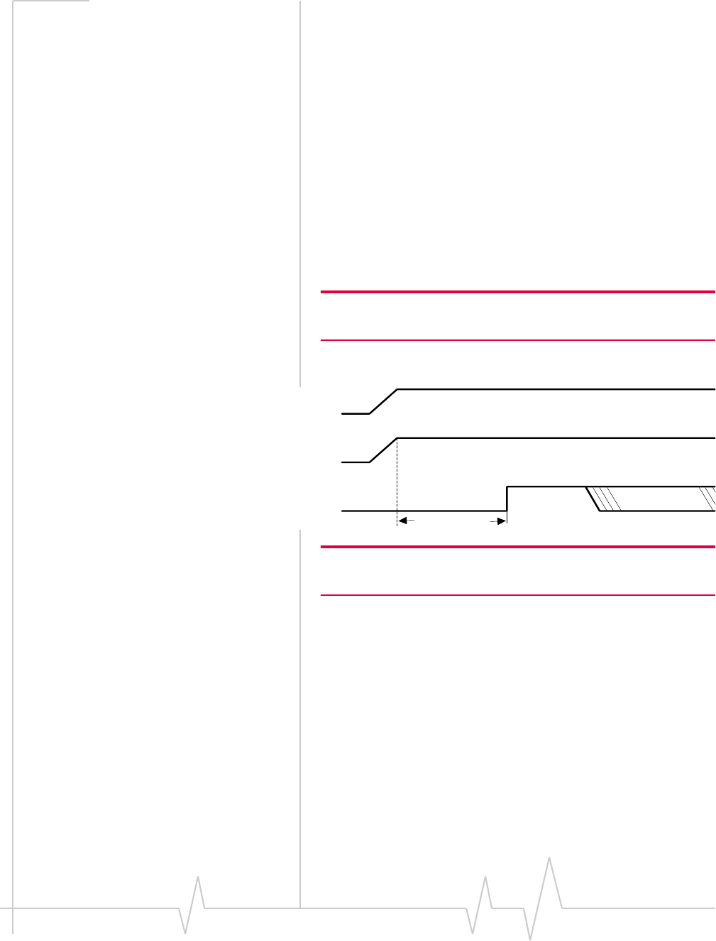
Power-up timing
TheunitisreadytoenumeratewithaUSBhostwithina
maximumof5.1seconds(dependingonmoduletype)after
power‐up.(Mostmodulesenumeratewithin4seconds.)
Note: The actual startup time may vary between the different module
types (for example, MC5725 versus MC8775).
Figure 2-6: Power-up timing diagram
Note: Startup time is the time after power-up when the modem is
ready to begin the enumeration sequence.
Transmit power wave form
(GSM)
AsshowninFigure2‐7,atmaximumGSMtransmitpower,the
inputcurrentcanremainat2.4Aforupto25%ofeach4.6ms
GSMcycle(1.15ms).ForClass12operation,thepeakcould
remainfor2.3ms(fourtimeslots).The2.4Acurrentdrawis
for50ohmsystems(1:1VSWR).Forworst‐caseantenna
designs,suchas3.5:1VSWR(asstatedinTable2‐5),this
currentdrawcouldincreasefrom2.4Ato2.75A,asshownin
Enumeration
3.3V
W_Disable#
USB D+
Startup time

Power Interface
Rev 1.9.1 Feb.09 Proprietary and Confidential 27
In the event of a discrepancy in values between this guide and the Product Specification Document (PSD), the PSD takes precedence.
thediagram.Beyondthe3.5:1VSWRasrecommendedtobe
worst‐caseinTableA‐5,thecurrentdrawcouldincrease
beyond2.75Ato3.5A.
AtmaximumGSMtransmitpower,theinputcurrentcan
remainat2.4Aforupto25%ofeach4.6msGSMcycle
(1.15ms)afterinitiallyreachingapeakof2.75Aaverageover
100μsandwithaninstantaneouspeakcurrentof3.5A.
Figure 2-7: GSM transmit power wave form
Current consumption
Currentconsumptiondependsonthemodule’soperating
modeatanygiventime.
Thissectiondescribes:
•Currentconsumptionforbothmoduletypes(MC57xxand
MC87xx)
•Operatingmodes
Current consumption overview
Note: Values in this guide are
taken from the appropriate
product specification documents
(PSDs) (listed in
Related
documents
, page 13) — in the
case of a discrepancy between
this document and the relevant
PSD, use the value listed in the
PSD.
Electricalrequirementsandcurrentspecificationsarelistedin
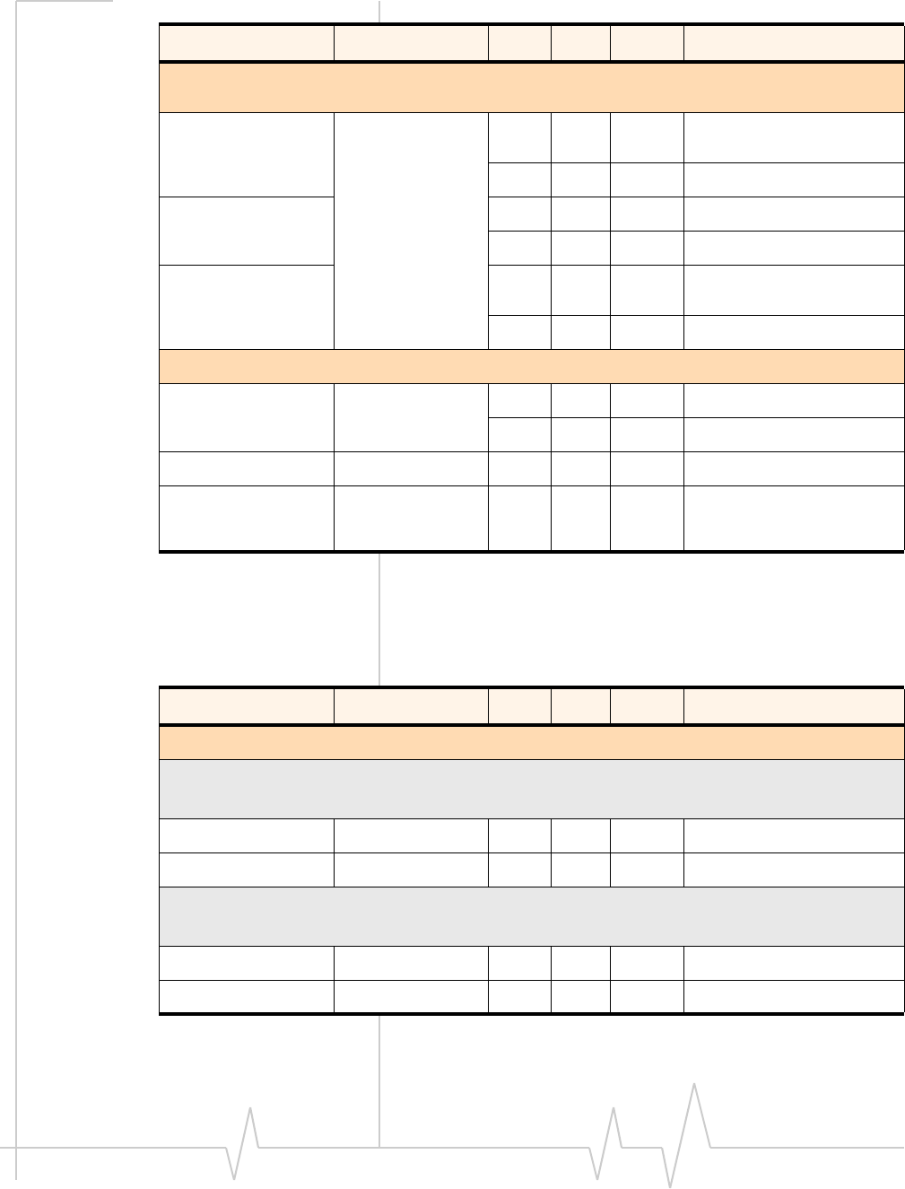
Table2‐3(MC57xx),Table2‐4(MC8775/MC8775V),Table2‐5
(MC8780/MC8781),Table2‐6(MC8785V),andTable2‐7
(MC8790/MC8790V/MC8791V/MC8792V).Thesespecifica‐
tionsidentifyminimum,typical,andmaximumcurrentdrain
foreachoperatingmode(whileintheNormalstate):
•Transmit
•Receive
•Sleep
•Deepsleep
•Shutdown
Thecurrentconsumptionvaluesinthesetablesweremeasured
usingasupplyvoltageof3.3V. Thedevice’ssupplyvoltageis
3.0–3.6Vwithatypicalvoltageof3.3V.
2.4
0.15
Current
(A)
2.75A peak
2.75
25 µs
1.15 ms 4.6 ms
3.5:1 VSWR = 2.75A
1:1 VSWR = 2.40A

CDMA and GSM / UMTS Mini Card Hardware Integration Guide
28 Proprietary and Confidential 2130114
In the event of a discrepancy in values between this guide and the Product Specification Document (PSD), the PSD takes precedence.
Note: For sleep modes, the values shown are for the actual sleep
state. The module wakes at intervals to control timing and check for
traffic — at these moments the current consumption is higher
Table 2-3: Current specifications (MC57xx)
Current consumption
(mA)
Condition Min Typical Max
CDMA Transmitting
CDMA Transmitting (MC5728/MC5728V)
Current depends on the radio band in use and the
network’s control of the module’s output power.
The ‘Typical’ value is based on:
250
TBD
300
TBD
950
TBD
CDMA Receiving
CDMA Receiving (MC5728/MC5728V)
90
TBD
100
TBD
120
TBD
CDMA Sleep (default slot cycle = 2)
CDMA Sleep, MC5728/MC5728V (default slot
cycle = 2)
The module supports slotted mode operation and Quick
Paging Channel (both enable reduced sleep current).
The values shown are the lowest power consumption
during the sleep cycle.
The default Slot Cycle Index (SCI) for slotted mode
operation is determined by the PRI setting (usually 1).
1.4
TBD
1.7
TBD
1.75
TBD
Deep Sleep Average
Deep Sleep Average (MC5728/MC5728V)
0.5
TBD
0.7
TBD
1.5
TBD
Shutdown
Shutdown (MC5728/MC5728V)
0.25
TBD
0.30
TBD
0.35
TBD
.
•40% full rate, and
•60% 1/8th rate over -35 to +23.5 dBm.
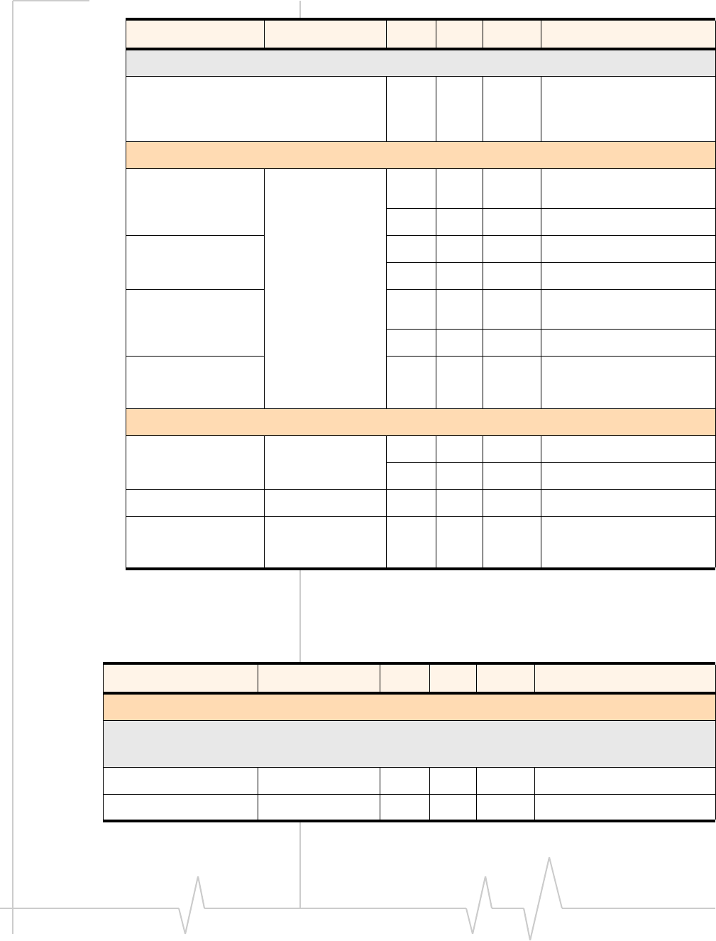
Table 2-4: Current specifications (MC8775 / MC8775V)
Description Band Typ Max Units Notes / Configuration
Averaged standby DC current consumption
With Sleep mode activated
(assumes USB bus is fully suspended during measurements)
HSDPA / WCDMA Bands I, II, V 2.9 4mA DRX cycle = 8 (2.56 s)
GSM / GPRS / EDGE All 2.8 4mA MFRM = 5 (1.175 s)

Power Interface
Rev 1.9.1 Feb.09 Proprietary and Confidential 29
In the event of a discrepancy in values between this guide and the Product Specification Document (PSD), the PSD takes precedence.
With Sleep mode deactivated
(assumes USB bus is fully suspended during measurements)
HSDPA / WCDMA Bands I, II, V 73 80 mA DRX cycle = 8 (2.56 s)
GSM / GPRS / EDGE All 46 55 mA MFRM = 5 (1.175 s)
Low Power Mode (LPM) / Offline Mode
RF disabled, but module is operational 2.5 4mA This state is entered when
Watcher® (or other
application) shuts down /
turns off the radio.
Averaged WCDMA / HSDPA DC current consumption
WCDMA talk current
(AMR 12.2 kbps
vocoder)
Bands I, II, V 300 -mA 0 dBm Tx power
480 -mA +15 dBm Tx power
650 -mA +21 dBm Tx power
WCDMA data current 330 -mA 64 kbps UL / 384 kbps DL,
+0 dBm Tx power
WCDMA searching
channels 180 mA 320 mA peak
HSDPA current 340 -mA 0 dBm Tx power
Maximum peak talk
current -1.2 AMax RF output power, full
rate, full operating
temperature range
Averaged GSM / EDGE DC current consumption
GSM Talk current
(Full rate GSM
vocoder, averaged
over multiple Tx
frames)
Quad GSM 300 -mA +5 dBm Tx power
210 -mA +13 dBm Tx power
300 -mA +29 dBm Tx power
GSM850 &
GSM900 360 -mA +33 dBm Tx power
GPRS current
(+13 dBm Tx power,
GPRS CS2, averaged
over multiple Tx
frames)
Quad GSM 180 -mA 1 Rx / 1 Tx slot
180 -mA 2 Rx / 1 Tx slot
240 -mA 4 Rx / 2 Tx slot
GSM / GPRS
searching channels Quad GSM,
GSM850, GSM900 163 mA 489 mA peak
Table 2-4: Current specifications (MC8775 / MC8775V) (Continued)
Description Band Typ Max Units Notes / Configuration
CDMA and GSM / UMTS Mini Card Hardware Integration Guide
30 Proprietary and Confidential 2130114
In the event of a discrepancy in values between this guide and the Product Specification Document (PSD), the PSD takes precedence.
EDGE current
(14 dBm Tx Power,
averaged over
multiple Tx frames)
Quad GSM 180 -mA 1 Rx / 1 Tx slot
180 -mA 2 Rx / 1 Tx slot
240 -mA 4 Rx / 2 Tx slot
Maximum Peak Talk
current Quad GSM 2.3 2.75 AMax RF output power, Tx
pulse current, full operating
temperature range
Miscellaneous DC current consumption
Module OFF leakage
current All 310 600 μAFull operating temperature
range
USB transmit current All -10 mA Full speed USB connection,
CL = 50 pF on D+ and D-
signals
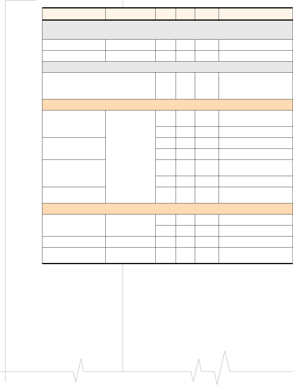
Table 2-5: Current specifications (MC8780 / MC8781)
Description Band Typ Max Units Notes / Configuration
Averaged standby DC current consumption
With Sleep mode activated
(assumes USB bus is fully suspended during measurements)
HSDPA / WCDMA UMTS bands 3 4 mA DRX cycle = 8 (2.56 s)
GSM / GPRS / EDGE GSM bands 3 4 mA MFRM = 5 (1.175 s)
With Sleep mode deactivated
(assumes USB bus is fully suspended during measurements)
HSDPA / WCDMA UMTS bands 46 50 mA DRX cycle = 8 (2.56 s)
GSM / GPRS / EDGE GSM bands 50 55 mA MFRM = 5 (1.175 s)
Low Power Mode (LPM) / Offline Mode
RF disabled, but module is operational 3 4 mA This state is entered when
Watcher (or other
application) shuts down /
turns off the radio.
Table 2-4: Current specifications (MC8775 / MC8775V) (Continued)
Description Band Typ Max Units Notes / Configuration
Power Interface
Rev 1.9.1 Feb.09 Proprietary and Confidential 31
In the event of a discrepancy in values between this guide and the Product Specification Document (PSD), the PSD takes precedence.
(Maximum power) Averaged WCDMA / HSDPA data current consumption (includes USB bus
current)
WCDMA UMTS bands 800 mA 384 kbps at 20 dBm Tx
powera
300 mA 0 dBm Tx power
HSUPA 850 mA 2 Mbps at 20 dBm Tx power
400 mA 0 dBm Tx power
HSDPA
(1.8 Mbps / 3.6 Mbps /
7.2 Mbps)
850 mA All speeds at 20 dBm Tx
powerb
450 mA 0 dBm Tx power
(Maximum power) Averaged GSM / EDGE data current consumption (includes USB bus current)
GSM / GPRS GSM bands 560 mA Max PCL for each bandc
230 mA 10 dBm Tx
EDGE GSM bands 520 mA Class 12c
Peak current
(averaged over
100 μs)
GSM bands 2.75 AWorst case on 850 / 900
band.
a. Highest current is on Band II (PCS1900)
b. Approximate current difference between speeds = 20 mA
Example: Current(7.2 Mbps) = Current(3.6 Mbps) + 20 mA = Current(1.8 Mbps) + 40 mA
c. Highest current is on 850 / 900 band Class 10 (Class 12 implements power backoff). Current on 1800 /
900 bands is typically 100–200 mA less.
Table 2-6: Current specifications (MC8785V)
Description Band Typ Max Units Notes / Configuration
Averaged standby DC current consumption
With Sleep mode activated
(assumes USB bus is fully suspended during measurements)
HSDPA / WCDMA UMTS bands 4 5 mA DRX cycle = 8 (2.56 s)
GSM / GPRS / EDGE GSM bands 4 5 mA MFRM = 5 (1.175 s)
With Sleep mode deactivated
(assumes USB bus is fully suspended during measurements)
HSDPA / WCDMA UMTS bands 96 100 mA DRX cycle = 8 (2.56 s)
GSM / GPRS / EDGE GSM bands 96 100 mA MFRM = 5 (1.175 s)
Table 2-5: Current specifications (MC8780 / MC8781) (Continued)
Description Band Typ Max Units Notes / Configuration
CDMA and GSM / UMTS Mini Card Hardware Integration Guide
32 Proprietary and Confidential 2130114
In the event of a discrepancy in values between this guide and the Product Specification Document (PSD), the PSD takes precedence.
Low Power Mode (LPM) / Offline Mode
RF disabled, but module is operational 4 5 mA This state is entered when
Watcher (or other
application) shuts down /
turns off the radio.
Averaged Call Mode WCDMA / HSDPA data DC power consumption
WCDMA UMTS bands 700 mA 384 kbps at 20 dBm Tx
powera
300 mA 0 dBm Tx power
HSUPA 750 mA 2 Mbps at 20 dBm Tx power
340 mA 0 dBm Tx power
HSDPA
(1.8 Mbps / 3.6 Mbps /
7.2 Mbps)
750 mA All speeds at 20 dBm Tx
powerb
340 mA 0 dBm Tx power
Peak current
(averaged over
100 μs)
780 mA
Averaged Call Mode GSM / EDGE data DC power consumption (with 4 time slots)
GSM / GPRS GSM bands 650 mA Max PCL for each bandc
220 mA 10 dBm Tx
EDGE GSM bands 670 mA Class 12c
Peak current
(averaged over
100 μs)
GSM bands 2.5 AWorst case on 850 / 900
band.
a. Highest current is on Band II (PCS1900)
b. Approximate current difference between speeds = 30 mA
c. Highest current is on 850 / 900 band Class 10 (Class 12 implements power backoff). Current on 1800 /
900 bands is typically 100–200 mA less.
Table 2-7: Current specifications (MC8790 / MC8790V / MC8791V / MC8792V)
Description Band Typ Max Units Notes / Configuration
Averaged standby DC current consumption
With Sleep mode activated
(assumes USB bus is fully suspended during measurements)
HSDPA / WCDMA UMTS bands 4 5 mA DRX cycle = 8 (2.56 s)
GSM / GPRS / EDGE GSM bands 4 5 mA MFRM = 5 (1.175 s)
Table 2-6: Current specifications (MC8785V) (Continued)
Description Band Typ Max Units Notes / Configuration
Power Interface
Rev 1.9.1 Feb.09 Proprietary and Confidential 33
In the event of a discrepancy in values between this guide and the Product Specification Document (PSD), the PSD takes precedence.
With Sleep mode deactivated
(assumes USB bus is fully suspended during measurements)
HSDPA / WCDMA UMTS bands 40 50 mA DRX cycle = 8 (2.56 s)
GSM / GPRS / EDGE GSM bands 40 50 mA MFRM = 5 (1.175 s)
Low Power Mode (LPM) / Offline Mode
RF disabled, but module is operational 4 5 mA This state is entered when
Watcher (or other application)
shuts down / turns off the
radio.
Averaged Call Mode WCDMA / HSDPA data DC power consumption
WCDMA UMTS bands 700 mA 384 kbps at 20 dBm Tx
powera
300 mA 0 dBm Tx power
HSUPA 800 mA 2 Mbps at 20 dBm Tx power
350 mA 0 dBm Tx power
HSDPA
(1.8 Mbps / 3.6 Mbps /
7.2 Mbps)
800 mA All speeds at 20 dBm Tx
powerb
370 mA 0 dBm Tx power
Peak current (averaged
over 100 μs) 720 mA
Averaged Call Mode GSM / EDGE data DC power consumption (with 4 time slots)
GSM / GPRS GSM bands 650 mA Max PCL for each bandc
300 mA 10 dBm Tx
EDGE GSM bands 620 mA Class 12c
Peak current (averaged
over 100 μs) GSM bands 2.6 AWorst case on 850 / 900
band.
a. Highest current is on Band II (PCS1900)
b. Approximate current difference between speeds = 30 mA
c. Highest current is on 850 / 900 band Class 10 (Class 12 implements power backoff). Current on 1800 / 900
bands is typically 100–200 mA less.
Table 2-7: Current specifications (MC8790 / MC8790V / MC8791V / MC8792V)
Description Band Typ Max Units Notes / Configuration

Table 2-8: Miscellaneous DC power consumption (MC8780 / MC8781 / MC8785V /
MC8790 / MC8790V / MC8791V / MC8792V)
Signal Description Band Typ Max Units Notes / Configuration
VCC Module OFF
leakage current All bands 400 600 μAFull operating temperature
range
USB transmit
current All bands 10 10 mA Full speed USB connection,
CL = 50 pF on D+ and D-
signals
CDMA and GSM / UMTS Mini Card Hardware Integration Guide
34 Proprietary and Confidential 2130114
In the event of a discrepancy in values between this guide and the Product Specification Document (PSD), the PSD takes precedence.
Modes
Transmit and Receive modes
Currentconsumptionintransmitorreceivemode(inacallor
dataconnection)isaffectedbyseveralfactors,suchas:
•Radiobandbeingused
•Transmitpower
•Receivegainsettings
•Datarate
•NumberofactiveTransmittimeslots(fortransmitmode)
Sleep mode
Sleepmodeisthenormalstateofthemodulebetweencallsor
dataconnections.Inthisreducedpowermode,themodule
cyclesbetweenwake(pollingthenetwork)andsleep,atan
intervaldeterminedbythenetworkprovider.
Deep sleep
Deepsleepmodeisareducedpower,out‐of‐network‐coverage
mode,thatthemoduleenterswhenitcannotacquirenetwork
serviceafterseveralminutes.
Themodulethenexitsdeepsleepperiodicallytotrytoacquire
service,andifsuccessful,attemptstoregister.
Shutdown mode
Whileinshutdownmode,themoduleispoweredoff,butstill
drawsaminimalcurrentfromthehostpowersupply.
SED (Smart Error Detection)
(MC87xxonly)
TheMC87xxmodemusesaformofSEDtotrackrecurrent
prematuremodemresets.Insuchcases,themodemautomati‐
callyforcesapauseinboot‐and‐holdmodeatpower‐onto
acceptanexpectedfirmwaredownloadtoresolvetheproblem.
Power Interface
Rev 1.9.1 Feb.09 Proprietary and Confidential 35
In the event of a discrepancy in values between this guide and the Product Specification Document (PSD), the PSD takes precedence.
TheSEDprocessisimplementedasfollows:
•Themodemtracksconsecutiveresetsofthemodemwithin
30secondsofpower‐on.
•Afterathirdconsecutiveresetoccurs,themodemautomati‐
callywaitsupto30secondsinboot‐and‐holdmode,
waitingforafirmwaredownloadtoresolvethepower‐cycle
problem.
•After30seconds(ifnofirmwaredownloadbegins),the
modemcontinuestopower‐on.
•Ifthemodemresetsagainwithin30secondsofpower‐on,
themodemagainwaitsinboot‐and‐holdmode.
Thisprocesscontinuesuntiltheunexpectedpower‐cycleissue
isresolved—eitherafirmwaredownloadoccurs,orthe
modemdoesn’tresetspontaneouslywithin30secondsof
power‐on.
Usage models
Usagemodelscanbeusedtocalculateexpectedcurrent
consumption.AsampleusagemodelisprovidedinTable2‐9,
basedonthevaluesinTable2‐3foraCDMAmodule.
Thisexamplemodelappliestoabattery‐operateddevice.In
practice,becausethemoduleisisolatedfromthebattery(the
hostdevicemanagesthepowersource),themAhratings
dependonthedevice’ssupplyefficiency.
Themoduleautomaticallyentersslottedsleepmodewhen
thereisnotransmissionorreceptionoccurring(SCI=2).
Transmitpowerisassumedtobe+3dBm.
Table 2-9: Power consumption of a sample application
Used by a field worker
(data only) Used for remote data
logging
Upload (module
Tx) 1000 kB/day 40 kB/h
Download
(module Rx) 500 kB/day 100 kB/day
Coverage / data
rate 1X / 80 kbps IS-95 / 14.4 kbps
Hours of
operation 8/day (off 16 hrs/day) 24/day
Total power
consumed over
24 hours
60 mAh 200 mAh

CDMA and GSM / UMTS Mini Card Hardware Integration Guide
36 Proprietary and Confidential 2130114
In the event of a discrepancy in values between this guide and the Product Specification Document (PSD), the PSD takes precedence.
3
Rev 1.9.1 Feb.09 Proprietary and Confidential 37
In the event of a discrepancy in values between this guide and the Product Specification Document (PSD), the PSD takes precedence.
3: RF Integration
ThischapterprovidesinformationrelatedtotheRF(Radio
Frequency)integrationoftheMC57xxandMC87xxmodules
withhostdevices.Thefrequenciesofoperationandperfor‐
mancespecificationsvarydependingonthemodulemodel
used.RFperformanceparametersfortypicalmodulesare
listedinTable3‐1andTable3‐2.
Note: Values in this guide are taken from the appropriate product
specification documents (PSDs) (listed in
Related documents
,
page 13) — in the case of a discrepancy between this document and
the relevant PSD, use the value listed in the PSD.
Table 3-1: MC57xx — Typical RF parameters
Band Tx Band
(MHz) Tx Power
(dBm) Rx Band
(MHz) Rx Sensitivity
(dBm)
PCS 1851–1910 +23 to +25 1930–1990 < -106
Cellular 824–849 +23 to +25 869–894 < -106
GPS 1575.42 SA Off: -148
SA On: -152
Table 3-2: MC87xx— RF parameters
Product Band Frequencies
(MHz) Conducted Rx
Sensitivity (dBm) GPS
Conducted
Sensitivity
Conducted
Transmit
Power
Typical Maximum (dBm) (dBm)
MC8775
MC8775V
MC8780
MC8781
MC8785V
MC8790
MC8790V
MC8791V
MC8792V
GSM 850
(2%) CS Tx: 824–849
Rx: 869-894 -107.5 -106 +32 ± 1 (GMSK)
+27 ± 1 (8PSK)
EGSM 900
(2%) CS Tx: 880-915
Rx: 925-960 -107.5 -106 +32 ± 1 (GMSK)
+27 ± 1 (8PSK)
DCS 1800
(2%) CS Tx: 1710-1785
Rx: 1805-1880 -106.5 -105 +29 ± 1 (GMSK)
+26 ± 1 (8PSK)
PCS 1900
(2%) CS Tx: 1850-1910
Rx: 1930-1990 -106.5 -105 +29 ± 1 (GMSK)
+26 ± 1 (8PSK)

CDMA and GSM / UMTS Mini Card Hardware Integration Guide
38 Proprietary and Confidential 2130114
In the event of a discrepancy in values between this guide and the Product Specification Document (PSD), the PSD takes precedence.
MC8775
MC8775V
MC8780
MC8781
MC8785V
MC8790
MC8790V
MC8791V
MC8792V
Band I
UMTS 2100
(0.1%) 12.2 kbps
Tx: 1920–1980
Rx: 2110–2170 -110.5 -109 +23 ± 1
MC8775
MC8775V
MC8780
MC8781
MC8785V
MC8790
MC8790V
MC8792V
Band II
UMTS 1900
(0.1%) 12.2 kbps
Tx: 1850–1910
Rx: 1930–1990 -110.5 -109 +23 ± 1
MC8775
MC8775V
MC8780
MC8781
MC8785V
MC8790
MC8790V
Band V
UMTS 850
(0.1%) 12.2 kbps
(Band VI is
included as a
subset of
Band V)
Tx: 824–849
Rx: 869–894 -111.5 -110 +23 ± 1
MC8792V Band VIII
UMTS 900
(0.1%) 12.2 kbps
Tx: 880–915
Rx: 925–960 -110.5 -109 +23 ± 1
MC8775V
MC8780
MC8781
MC8785V
MC8790
MC8790V
MC8791V
MC8792V
GPS 1575.42 -154
Table 3-2: MC87xx— RF parameters (Continued)
Product Band Frequencies
(MHz) Conducted Rx
Sensitivity (dBm) GPS
Conducted
Sensitivity
Conducted
Transmit
Power
Typical Maximum (dBm) (dBm)
RF Integration
Rev 1.9.1 Feb.09 Proprietary and Confidential 39
In the event of a discrepancy in values between this guide and the Product Specification Document (PSD), the PSD takes precedence.
RF connection
Whenattachinganantennatothemodule:
Note: To disconnect the
antenna, make sure you use the
Hirose U.FL connector removal
tool (P/N UFL-LP-N-2(01)) to
prevent damage to the module
or coaxial cable assembly.
•UseaHiroseU.FLconnector(model
U.FL#CL331‐0471‐0‐10)toattachanantennatoa
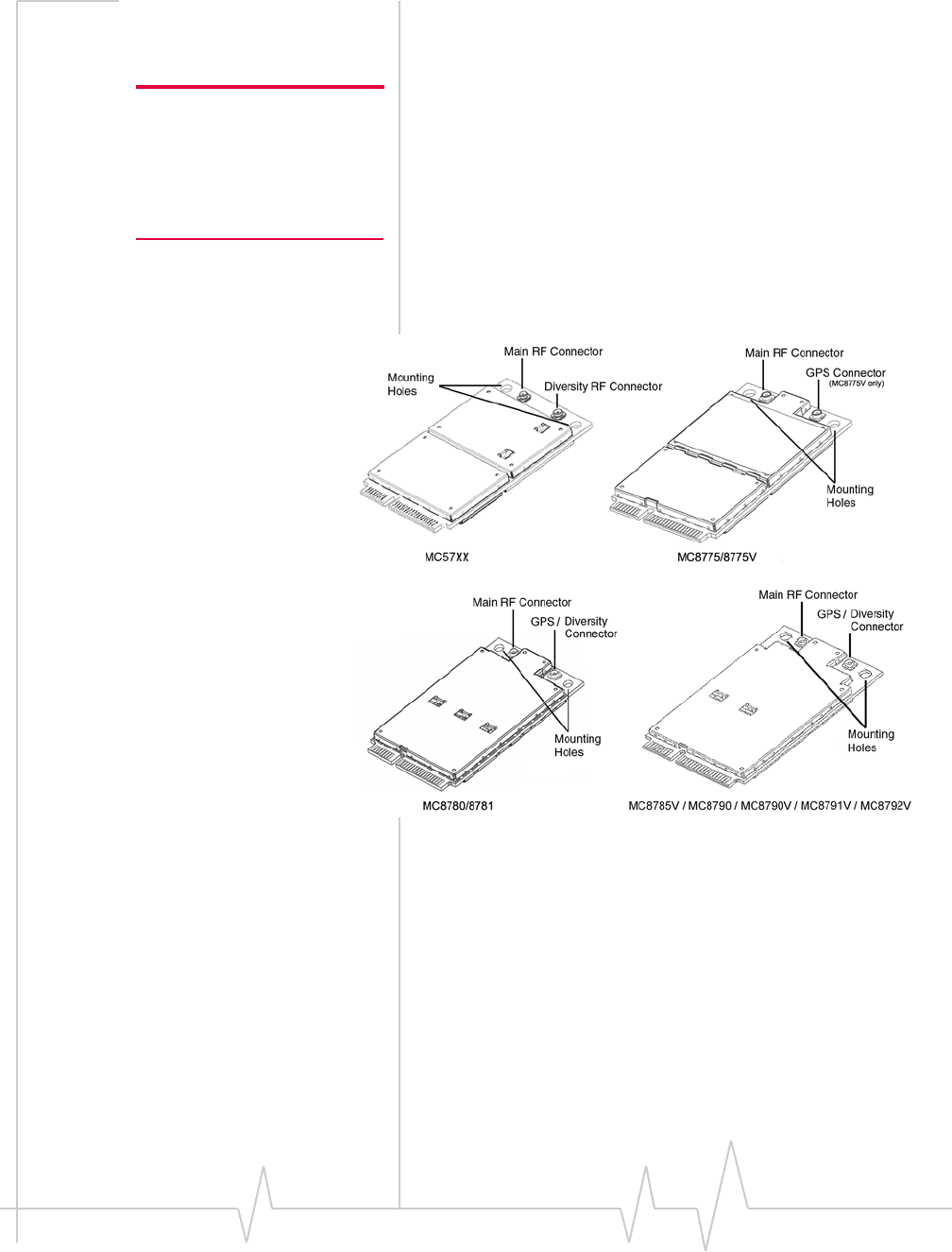
connectionpointonthemodule,asshowninFigure3‐1(the
mainRFconnectoronthetopside;thediversityRForGPS
connectoronthebottomside).
•Matchcoaxialconnectionsbetweenthemoduleandthe
antennato50Ω.
•MinimizeRFcablelossestotheantenna;therecommended
maximumcablelossforantennacablingis0.5dB.
Figure 3-1: Antenna connection points and mounting holes
Ground connection
Whenconnectingthemoduletosystemground:
•Preventnoiseleakagebyestablishingaverygoodground
connectiontothemodulethroughthehostconnector.
•Connecttosystemgroundusingthetwomountingholesat
thetopofthemodule(asshowninFigure3‐1).
•MinimizegroundnoiseleakageintotheRF.
Dependingonthehostboarddesign,noisecouldpotentially
becoupledtothemodulefromthehostboard.Thisis

CDMA and GSM / UMTS Mini Card Hardware Integration Guide
40 Proprietary and Confidential 2130114
In the event of a discrepancy in values between this guide and the Product Specification Document (PSD), the PSD takes precedence.
mainlyanissueforhostdesignsthathavesignalstraveling
alongthelengthofthemodule,orcircuitryoperatingat
bothendsofthemoduleinterconnects.
Shielding
ThemoduleisfullyshieldedtoprotectagainstEMIandto
ensurecompliancewithFCCPart15‐“RadioFrequency
Devices”(orequivalentregulationsinotherjurisdictions).
Note: The module shields must NOT be removed.
Antenna and cabling
Note: Values in this guide are
taken from the appropriate
product specification documents
(PSDs) (listed in
Related
documents
, page 13) — in the
case of a discrepancy between
this document and the relevant
PSD, use the value listed in the
PSD.
Whenselectingtheantennaandcable,itiscriticaltoRFperfor‐
mancetomatchantennagainandcableloss.
Choosing the correct antenna and cabling
Considerthefollowingpointsforpropermatchingofantennas
andcabling:
•Theantenna(andassociatedcircuitry)shouldhavea
nominalimpedanceof50Ωwithareturnloss≤ 10dB
acrosseachfrequencybandofoperation.
•Thesystemgainvalueaffectsbothradiatedpowerand
regulatory(FCC,IC,CE,etc.)testresults.
Developing custom antennas
Considerthefollowingpointswhendevelopingcustom‐
designedantennas:
•AskilledRFengineershoulddothedevelopmenttoensure
thattheRFperformanceismaintained.
•Identifythebandsthatneedtobesupported,particularly
whenboththeMC57xxandMC87xxwillbeinstalledinthe
sameplatform.Inthiscase,youmaywanttodevelop
separateantennasformaximumperformance.
Note: For detailed electrical performance criteria, see
Appendix A:
Antenna Specification
, page 101.
Determining the antenna’s location
Considerthefollowingpointswhendecidingwheretoputthe
antenna:
•AntennalocationmayaffectRFperformance.Althoughthe
moduleisshieldedtopreventinterferenceinmostapplica‐

RF Integration
Rev 1.9.1 Feb.09 Proprietary and Confidential 41
In the event of a discrepancy in values between this guide and the Product Specification Document (PSD), the PSD takes precedence.
tions,theplacementoftheantennaisstillveryimportant—
ifthehostdeviceisinsufficientlyshielded,highlevelsof
broadbandorspuriousnoisecandegradethemodule’s
performance.
•Connectingcablesbetweenthemoduleandtheantenna
musthave50Ωimpedance.Iftheimpedanceofthemodule
ismismatched,RFperformanceisreducedsignificantly.
•Antennacablesshouldberouted,ifpossible,awayfrom
noisesources(switchingpowersupplies,LCDassemblies,
etc.).Ifthecablesarenearthenoisesources,thenoisemay
becoupledintotheRFcableandintotheantenna.
Disabling the diversity antenna
•MC57xx—Ifyourhostdeviceisnotdesignedtousethe
MC57xxmodule’sdiversityantenna,terminatetheinterface
witha50Ωload.
•MC8780/MC8781/MC8785V/MC8790/MC8790V/
MC8791V/MC8792V—UsetheATcommand!RXDEN=0to
disablereceivediversityor !RXDEN=1toenablereceive
diversity.
Interference and sensitivity
Note: These modules are based
on ZIF (Zero Intermediate
Frequency) technologies; when
performing EMC
(Electromagnetic Compatibility)
tests, there are no IF
(Intermediate Frequency)
components from the module to
consider.
SeveralsourcesofinterferencecanaffecttheRFperformance
ofthemodule(RFdesense).Commonsourcesincludepower
supplynoiseanddevice‐generatedRF.
RFdesensecanbeaddressedthroughacombinationof
mitigationtechniquesandradiatedsensitivitymeasurement.
Power supply noise
NoiseinthepowersupplycanleadtonoiseintheRFsignal.
Note: Values in this guide are
taken from the appropriate
product specification documents
(PSDs) (listed in
Related
documents
, page 13) — in the
case of a discrepancy between
this document and the relevant
PSD, use the value listed in the
PSD.
Thepowersupplyripplelimitforthemoduleisnomorethan
200mVp‐p1Hzto100kHz.Thislimitincludesvoltageripple
duetotransmitterburstactivity.
Interference from other wireless devices
Wirelessdevicesoperatinginsidethehostdevicecancause
interferencethataffectsthemodule.
Todeterminethemostsuitablelocationsforantennasonyour
hostdevice,evaluateeachwirelessdevice’sradiosystem,
consideringthefollowing:
•Anyharmonics,sub‐harmonics,orcross‐productsofsignals
generatedbywirelessdevicesthatfallinthemodule’sRx

CDMA and GSM / UMTS Mini Card Hardware Integration Guide
42 Proprietary and Confidential 2130114
In the event of a discrepancy in values between this guide and the Product Specification Document (PSD), the PSD takes precedence.
rangemaycausespuriousresponse,resultingindecreased
Rxperformance.
•TheTxpowerandcorrespondingbroadbandnoiseofother
wirelessdevicesmayoverloadorincreasethenoisefloorof
themodule’sreceiver,resultinginRxdesense.
Theseverityofthisinterferencedependsontheclosenessof
theotherantennastothemodule’santenna.Todetermine
suitablelocationsforeachwirelessdevice’santenna,
thoroughlyevaluateyourhostdevice’sdesign.
Device-generated RF
Note: The module can cause
interference with other devices
such as hearing aids and on-
board speakers.
Wireless devices such as the
Mini Card transmit in bursts
(pulse transients) for set
durations (RF burst frequencies).
Hearing aids and speakers
convert these burst frequencies
into audible frequencies,
resulting in audible noise.
AllelectroniccomputingdevicesgenerateRFinterferencethat
cannegativelyaffectthereceivesensitivityofthemodule.
Theproximityofhostelectronicstotheantennainwireless
devicescancontributetodecreasedRxperformance.Compo‐
nentsthataremostlikelytocausethisinclude:
•Microprocessorandmemory
•Displaypanelanddisplaydrivers
•Switching‐modepowersupplies
Theseandotherhigh‐speeddevices(inparticular,the
processor)candecreaseRxperformancebecausetheyrunat
frequenciesoftensofMHz.Therapidriseandfallofthese
clocksignalsgenerateshigher‐orderharmonicsthatoftenfall
withintheoperatingfrequencybandofthemodule,affecting
themodule’sreceivesensitivity.
Example
Onasub‐systemrunningat40MHz,the22ndharmonicfalls
at880MHz,whichiswithinthecellularreceivefrequency
band.
Note: In practice, there are usually numerous interfering frequencies
and harmonics. The net effect can be a series of desensitized receive
channels.
Note: It is important to
investigate sources of localized
interference early in the design
cycle.
Methods to mitigate decreased Rx
performance
Toreducetheeffectofdevice‐generatedRFonRxperfor‐
mance:
•Puttheantennaasfaraspossiblefromsourcesofinter‐
ference.Thedrawbackisthatthemodulemaybeless
convenienttouse.

RF Integration
Rev 1.9.1 Feb.09 Proprietary and Confidential 43
In the event of a discrepancy in values between this guide and the Product Specification Document (PSD), the PSD takes precedence.
•Shieldthehostdevice.Themoduleitselfiswellshieldedto
avoidexternalinterference.However,theantennacannot
beshieldedforobviousreasons.Inmostinstances,itis
necessarytoemployshieldingonthecomponentsofthe
hostdevice(suchasthemainprocessorandparallelbus)
thathavethehighestRFemissions.
•Filteroutunwantedhigh‐orderharmonicenergybyusing
discretefilteringonlowfrequencylines.
•Formshieldinglayersaroundhigh‐speedclocktracesby
usingmulti‐layerPCBs.
•Routeantennacablesawayfromnoisesources.
Radiated sensitivity
measurement
Awirelessdevicecontainsmanysourcesofnoisethat
contributetoareductioninRxperformance.
Todeterminetheextentofanydesensitizationofreceiver
performanceduetoself‐generatednoiseinthehostdevice,
over‐the‐air(OTA)orradiatedtestingisrequired.Thistesting
canbeperformedbySierraWirelessoryoucanuseyourown
OTAtestchamberforin‐housetesting.
Sierra Wireless’ sensitivity testing and
desensitization investigation
Mostcarriersrequireacertainlevelofreceiverperformanceto
ensureproperfunctioningofthedeviceontheirnetworks.
Althoughthemodulehasbeendesignedtomeetthesecarrier
requirements,itisstillsusceptibletovariousperformance
inhibitors.
AspartoftheEngineeringServicespackage,SierraWireless
offersmodemOTAsensitivitytestinganddesensitization
(desense)investigation.Formoreinformation,contactyour
accountmanagerortheSalesDesk(seepage5).
Note: Sierra Wireless has the capability to measure TIS (Total
Isotropic Sensitivity) and TRP (Total Radiated Power) according to
CTIA's published test procedure.
OTA test chamber configuration
TomakeOTAmeasurements,atestchamberisrequired.A
full‐sizeanechoicchamberisnotnecessarilyrequired.
Figure3‐2showsasmallanechoicchambermanufacturedby

CDMA and GSM / UMTS Mini Card Hardware Integration Guide
44 Proprietary and Confidential 2130114
In the event of a discrepancy in values between this guide and the Product Specification Document (PSD), the PSD takes precedence.
Lindgren.Thisdoesnotprovidepowertothesameaccuracy
asafull‐sizeanechoicchamber,butissufficientforthisappli‐
cation.Abasestationsimulator,suchasanAgilent8960
(shown)orRohde&SchwarzCMU200,isusedtoprovideFER
(FrameErrorRate)measurements.
Figure 3-2: Anechoic chamber
Path loss calculation
Thechamberiscalibratedforpathlossusingareference
antennawithknowngainthatisfeedingaspectrumanalyzer
orpowermeter.Thismakesitpossibletodeterminethe
radiatedpoweravailabletothereceivingantennaandthepath
loss:
Radiated Power = Measured received power
+ Any cable losses
- Reference receive antenna gain
Path Loss = Radiated power
- Input power
Note: It is not necessary to know the gain of the transmitting antenna;
it is included in the path loss.
Approx . 1 m
Agilent 8960
call box

RF Integration
Rev 1.9.1 Feb.09 Proprietary and Confidential 45
In the event of a discrepancy in values between this guide and the Product Specification Document (PSD), the PSD takes precedence.
Positioning the DUT (Device Under Test)
Toachievemeaningfulresults,thedevicemustbepositioned
suchthatthepeakofthereceiveantennapatternispointed
towardthesourceantenna.Theoretically,thebestwayto
accomplishthisistomodifytheDUTsothatantennaoutputis
throughcoaxialcable.Thedeviceisthenrotateduntilthe
receivepowerismaximized.
Alternate path loss calculation method
Pathlosscanalsobecalculated,withoutmodifyingtheDUT,
byusingthetransmitcapabilitiesoftheunit.Thismethodof
calculationispossiblebecausethepositionthatmaximizes
transmitterpowerprovidesasufficientlyaccuratelocationfor
receiverdesensemeasurements.Theunitisplacedinacalland
settogeneratepeakoutputpower,eitherthroughatestmode,
orbyconfiguringthebasestationsimulatortoissuetheappro‐
priatecommand.Theunitisthenpositionedformaximum
powerasdeterminedbythecallbox.
Sensitivity vs. frequency
FortheMC57xx,sensitivityisdefinedastheinputpowerlevel
indBmthatproducesaFER(FrameErrorRate)of0.5%.Sensi‐
tivityshouldbemeasuredatallCDMAfrequenciesacross
eachband.Forexample,Figure3‐3illustratessensitivityinthe
USPCSband.Thereare25physicalchannelswithaspacingof
50KHz;thefirstCDMAchannelisCH25.
FortheMC87xx,sensitivityisdefinedastheinputpowerlevel
indBmthatproducesaBER(BitErrorRate)of2%(GSM)or
0.1%(UMTS).SensitivityshouldbemeasuredatallGSM/
UMTSfrequenciesacrosseachband,asshowninFigures3‐4
through3‐11.

CDMA and GSM / UMTS Mini Card Hardware Integration Guide
46 Proprietary and Confidential 2130114
In the event of a discrepancy in values between this guide and the Product Specification Document (PSD), the PSD takes precedence.
Sensitivity test results — MC57xx
Figure3‐3showstypicaltestresultsfortheUSPCSbandfor
bothconductedandover‐the‐airconnections.Theconducted
(orʺconnectorizedʺ)measurementsweremadeusinganRF
coaxialcableconnection.Theover‐the‐airmeasurementswere
madeusingbothanexternalantennaandatypicaldevice
antenna.
Figure 3-3: US PCS sensitivity measurements
Inthistest,theexternalantennaperformedbest—the
expectedresultifahighefficiencyantennawithsomegainis
used.Theinternalantennahaslessgainthantheexternal
antenna,sotheinternalantennaʹsperformanceisoffsetabove
theexternalantenna.Theantennagainmustbeknownto
determinewhethertheoffsetisstrictlytheresultofantenna
gainorifbroadbanddesenseispresent.Narrowbanddesense
canbeseenatchannels325,625,and925.
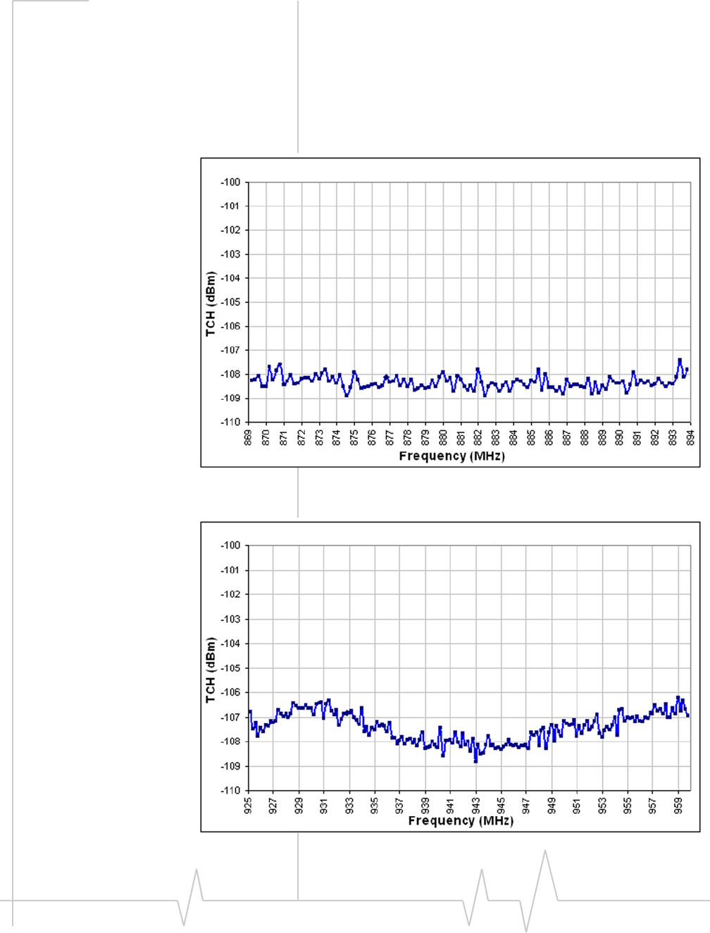
RF Integration
Rev 1.9.1 Feb.09 Proprietary and Confidential 47
In the event of a discrepancy in values between this guide and the Product Specification Document (PSD), the PSD takes precedence.
Sensitivity test results — MC87xx
Figures3‐4through3‐11showtypicaltestresultsfor
conductedconnectionsfortheGSM850,GSM900,GSM1800,
GSM1900,UMTS850,UMTS1900,andUMTS2100bands.The
conductedmeasurementsweremadeusinganRFcoaxialcable
connection.
Figure 3-4: GSM850 sensitivity for BERII < 2%
Figure 3-5: EGSM900 sensitivity for BERII < 2%

CDMA and GSM / UMTS Mini Card Hardware Integration Guide
48 Proprietary and Confidential 2130114
In the event of a discrepancy in values between this guide and the Product Specification Document (PSD), the PSD takes precedence.
Figure 3-6: DCS1800 sensitivity for BERII < 2%
Figure 3-7: PCS1900 sensitivity for BERII < 2%
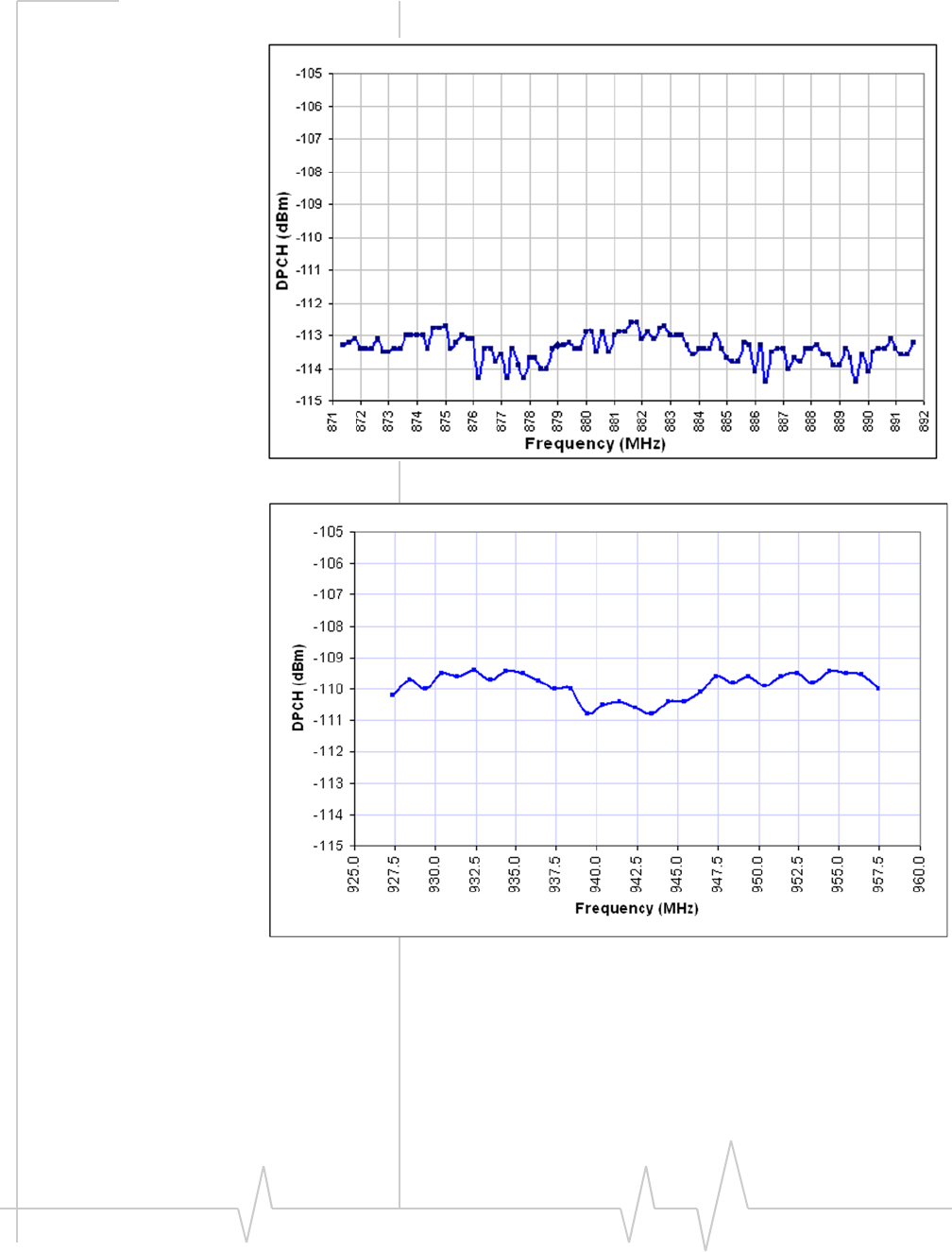
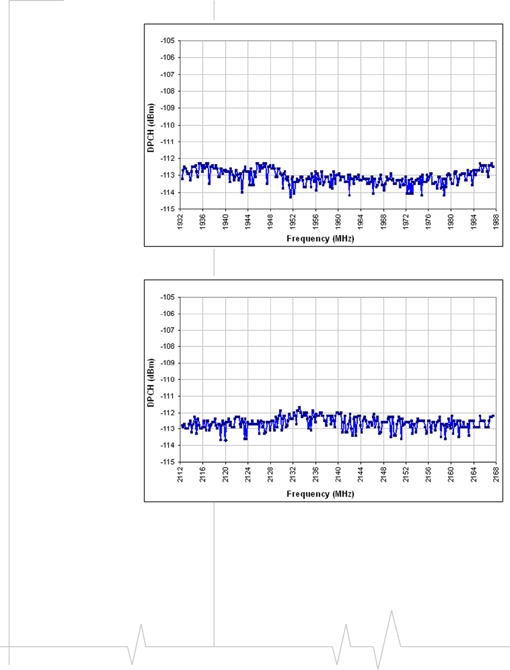
CDMA and GSM / UMTS Mini Card Hardware Integration Guide
50 Proprietary and Confidential 2130114
In the event of a discrepancy in values between this guide and the Product Specification Document (PSD), the PSD takes precedence.
Figure 3-10: UMTS1900 sensitivity for BER < 0.1%
Figure 3-11: UMTS2100 sensitivity for BER < 0.1%
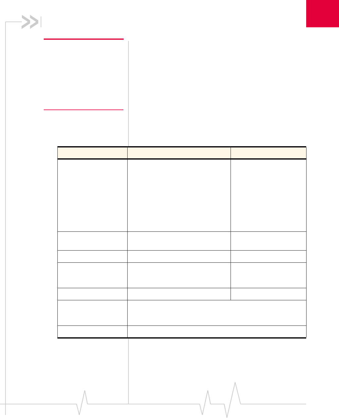
4
Rev 1.9.1 Feb.09 Proprietary and Confidential 51
In the event of a discrepancy in values between this guide and the Product Specification Document (PSD), the PSD takes precedence.
4: Audio Interface
Note: Values in this guide are
taken from the appropriate
product specification documents
(PSDs) (listed in
Related
documents
, page 13) — in the
case of a discrepancy between
this document and the relevant
PSD, use the value listed in the
PSD.
TheMC5725V/MC5727V/MC5728V/MC8775V/MC8785V/
MC8790V/MC8791V/MC8792Vmodulessupportfouraudio
modesthatmayberequiredbyahostaudiosystem:
•Handset
•Headset
•Carkit
•Speakerphone
Themodulessupportbothadifferentialanaloginterfaceand
PCMdigitalaudio,andallowdynamicrun‐timeselectionof
theappropriatemode.
Table4‐1summarizesthekeyaudiofeaturesofthesemodules.
Thesemodulesareintendedtoserveasanintegralcomponent
ofamorecomplexaudiosystem—forexample,aPDAwitha
separatecodecinterfacedtotheHostApplicationprocessor.
Table 4-1: Audio features
Feature Transmit Receive
Gain (adjustable) MC5725V / MC5727V — Up to
+16 dB analog gain
MC5728V — Programmable to 0 dB
or +24 dB
MC8775V / MC8785V / MC8790V /
MC8791V / MC8792V — Up to
+48.5 dB analog gain available
(when the analog interface is
selected)
Up to +12 dB
Filtering stages Several adjustable high-pass and
slope filters High-pass filter
Noise suppression Supported n/a
Echo cancellation Configurable for each audio mode
(headset, handset, speakerphone,
and car kit)
n/a
Output driver stage n/a Supported
FIR (Finite Impulse
Response) filtering MC87xx — Option of providing 13 tap FIR filtering for receive and
transmit paths to equalize the acoustic response of the speaker
and microphone elements.
Audio pass band 300 Hz–3.4 kHz
CDMA and GSM / UMTS Mini Card Hardware Integration Guide
52 Proprietary and Confidential 2130114
In the event of a discrepancy in values between this guide and the Product Specification Document (PSD), the PSD takes precedence.
Usually,theinterfacebetweenthemoduleandthehostaudio
systemissettoline‐levelamplitudeswithnotransducer
considerations.Theresponsibilityofthemodulecodecorhost
codecforspecialfunctionsisdetailedinTable4‐2.
System block diagrams
Note: When integrating the module into your host platform, make sure
the module has sufficient shielding to prevent RF interference.
MC5725V / MC5727V system block
Figure4‐1representstheMC5725V/MC5727Vmodule’saudio
systemblock,andincludesthefollowingfeatures:
•Moduleinterconnectsareshownontheleftsideofthe
diagram.Theaudiointerfaceusesthesignals:
·MIC_P/MIC_N
·SPK_P/SPK_N
Note: Make sure the host device
includes DC blocking capacitors
on the Audio In lines – the
module does not include series
capacitors.
•Dynamicrangesforeachprogrammablegainstageare
listed,withthefollowingconstraints:
·MIC_AMP1isprogrammableindiscretestepsonly
·CodecSTGain,whensettotheminimumsetting,effec‐
tivelymutessidetoneinthemodulecodec
Table 4-2: Functions - responsibility codecs
Function Responsible Codec
Phone oriented (e.g., echo
cancellation, FIR filtering) Module codec
Path-switching Host codec
Transducer interfaces Host codec
Adjustable gain / volume settings Either
DTMF / ringer tone generation Either
Mixing Host codec

Audio Interface
Rev 1.9.1 Feb.09 Proprietary and Confidential 53
In the event of a discrepancy in values between this guide and the Product Specification Document (PSD), the PSD takes precedence.
Figure 4-1: MC5725V / MC5727V Audio system block
MC5728V system block
Figure4‐2representstheMC5728Vmodule’saudiosystem
block,andincludesthefollowingfeatures:
•Moduleinterconnectsareshownontheleftsideofthe
diagram.Theaudiointerfaceusesthesignals:
·MIC_P/MIC_N
·SPK_P/SPK_N
Note: Make sure the host device
includes DC blocking capacitors
on the Audio In lines – the
module does not include series
capacitors.
•Dynamicrangesforeachprogrammablegainstageare
listed,withthefollowingconstraints:
·MIC_AMP1isprogrammableto0dBor+24dBonly
·CodecSTGain,whensettotheminimumsetting,effec‐
tivelymutessidetoneinthemodulecodec
Decoder
RX DAC
EncoderTX ADC
HPF &
Slope
HPF
Echo Cancellation
NS &
AAGC Tx FIR
Rx FIR 13K CELP/
EVRC
Decoder
AAGC
13 bit A/D
13 bit D/A
CodecRxGain
RX_HPF_DIS_N
CodecSTGain
CodecTxGain
TX_HPF_DIS_N
TX_SLOPE_FILT_DIS_N
MIC_AMP1_GAIN
+16dB
+8dB
+6dB
-2dB
nsSwitch TxPCMFilt TxVolume
RxVolume
RxPCMFilt
AMP_SEL
001 010 100
10 01
MIC_SEL
35mW @ +3dBm0
RF Filter
33n
22p
MIC_AMP2_BYP
PCM I/F
+12dB
-25dB
-84dB
+12dB
-3dB
-84dB
+12dB
0dB
-81dB
+12dB
-48dB
-96dB
+12dB
0dB
-84dB
57.3mVrms
@ 0dBm0
SPK_P
SPK_N
MIC_P
MIC_N
13K CELP/
EVRC
Encoder
DTMF
Encoder
DTMF Rx Gain
DTMF Tx Gain
DTMF
Decoder
Audio In
Audio Out
RF
Interface
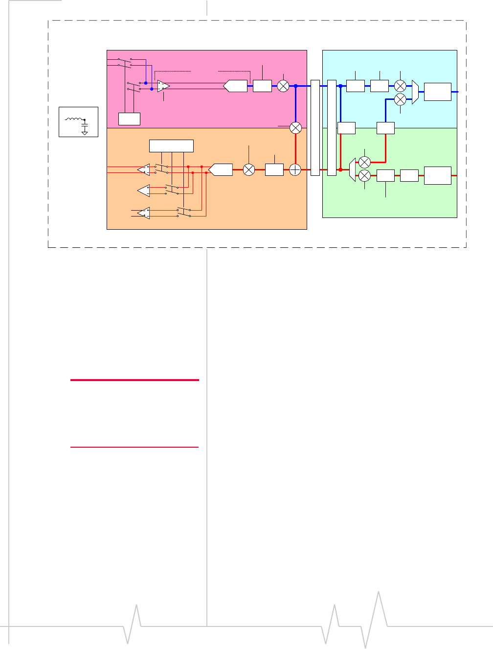
CDMA and GSM / UMTS Mini Card Hardware Integration Guide
54 Proprietary and Confidential 2130114
In the event of a discrepancy in values between this guide and the Product Specification Document (PSD), the PSD takes precedence.
Figure 4-2: MC5728V Audio system block
MC8775V / MC8785V / MC8790V / MC8791V / MC8792V
system block
Figure4‐3representstheMC8775V/MC8785V/MC8790V/
MC8791V/MC8792Vmodule’saudiosystemblock,and
includesthefollowingfeatures:
•Moduleinterconnectsareshownontheleftsideofthe
diagram.Theanalogaudiointerfaceusesthesignals:
·MIC_P/MIC_N
·SPK_P/SPK_N
Note: Make sure the host device
includes DC blocking capacitors
on the analog Audio In lines –
the module does not include
series capacitors.
•ThedigitalPCMaudiointerfaceusesthesignals:
·PCM_CLK
·PCM_DIN
·PCM_DOUT
·PCM_SYNC
•Dynamicrangesforeachprogrammablegainstageare
listed,withthefollowingconstraints:
·MIC_AMP1isprogrammablein1.5dBsteps
·CodecSTGain,whensettotheminimumsetting,effec‐
tivelymutessidetoneinthemodulecodec
•WhenPCMaudioisselected,theRXDACandTXADC
blocksarebypassed—theexternalPCMcodeccontrols
transmitgain,receivegain,andsidetonegain.
Decoder
RX DAC
EncoderTX ADC
HPF &
Slope
HPF
Echo Cancellation
NS &
AAGC Tx FIR
Rx FIR 13K CELP/
EV RC
Decoder
AAGC
13 bit A/D
13 bit D/A
CodecRxGain
RX_HPF_DIS_N
CodecSTGain
CodecTxGain
TX_HPF_DIS_N
TX_SLOPE_FILT_DIS_
N
MIC_ A MP1
0 dB or +24 dB
nsSw itch TxPCMFilt TxVolume
RxV olume
RxPCMFilt
AMP_SEL
MIC_SEL
35mW @ +3dBm0
RF Filter
33n
22
p
PCM I/F
+12dB
-25dB
-84dB
+12dB
-3dB
-84dB
+12dB
0dB
-84dB
0dB
-48dB
-96dB
+12dB
0dB
-84dB
57.3mVrms
@ 0dBm0
g
SPK1N
SPK1P
MIC1P
MIC1N
13K CELP/
EV RC
Encoder
DTMF
Encoder
DTMF Rx Gain
DTMF Tx Gain
DTMF
Decoder
Audio In
Audio Out
RF
Interfac
e
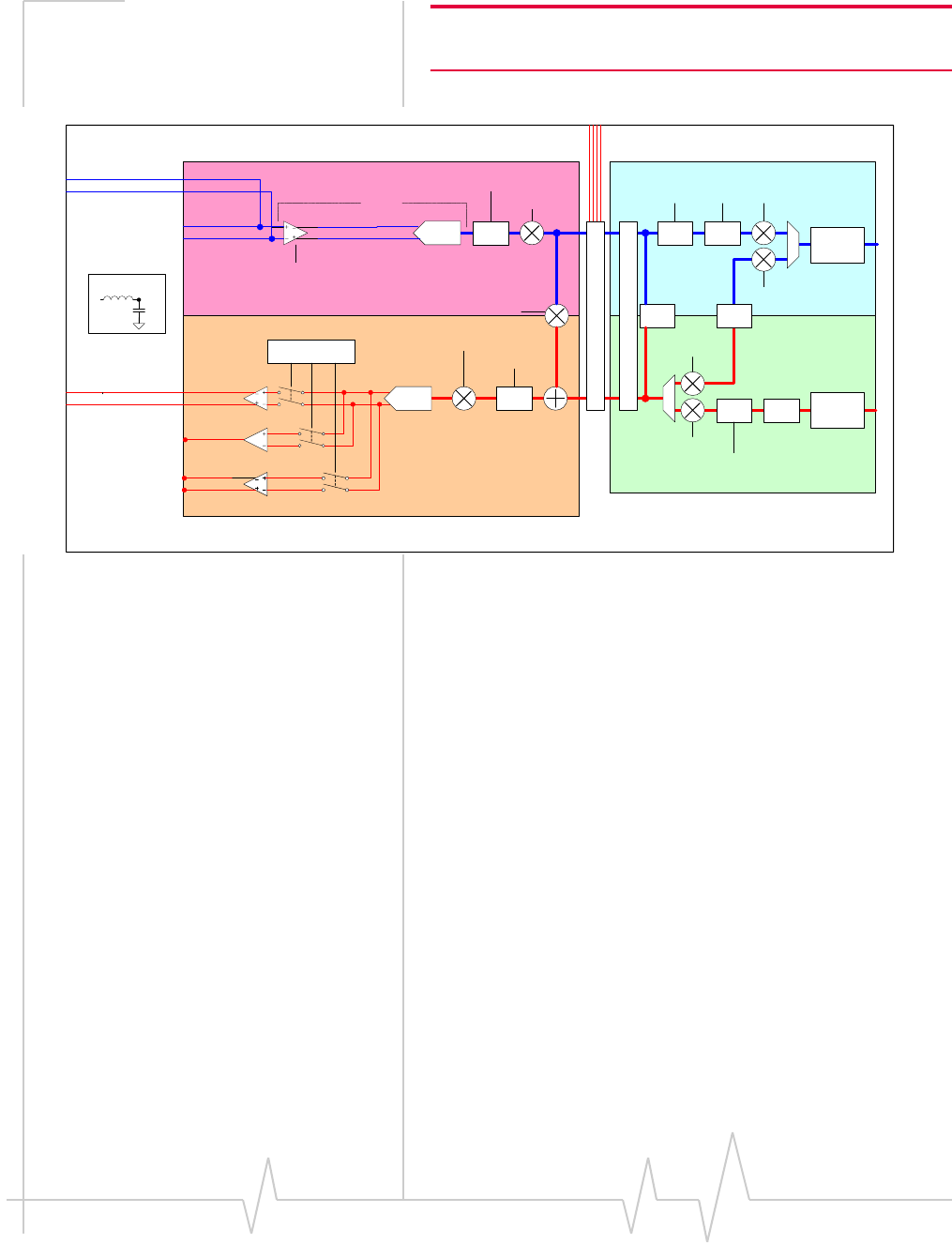
Audio Interface
Rev 1.9.1 Feb.09 Proprietary and Confidential 55
In the event of a discrepancy in values between this guide and the Product Specification Document (PSD), the PSD takes precedence.
Note: Data mixing is not supported. If mixing of voice signal is
required, it must be done by the host processor.
Figure 4-3: MC8775V / MC8785V / MC8790V / MC8791V / MC8792V Audio system block
Modes of operation
Thesemodulessupportfouroperationalmodes:headset,
handset,carkit,andspeakerphone—endproductscanuseany
combinationofthesemodes.
Thehostdevicemustusehost‐modemmessagingtotellthe
modulewhichmodetouseforeachcall.
Sidetone support
Thesidetonepathmixesthenear‐endtransmitvoicetothe
near‐endreceive.Thisgivesthenear‐endusersomefeedback
thatindicatesthatthecallisupandthattheaudiosystemis
functioning.
ThesidetonepathcanbeenabledineitherthePDAcodecor
theMiniCardmodem—eachpathisequallyvalid.Itshould
notbeaddedtobothdevices,andforspeakerphoneorcarkit
applications,bothsidetonepathsshouldbedisabled.
Thetypicalhandsetsidetoneis12dBbelowtransmitvoice
levels.
Decoder
RX DAC
EncoderTX ADC
HPF &
Slope
HPF
Echo Cancellation
NS &
AAGC Tx FIR
Rx FIR 13K CELP/
EVRC
Decoder
AAGC
13 bit A/D
13 bit D/A
CodecRxGain
RX_HPF_DIS_N
CodecSTGain
CodecTxGain
TX_HPF_DIS_N
TX_SLOPE_FILT_DIS_N
MIC_AMP1_GAIN
-6dB to +49.5dB
in 1.5dB steps
nsSwitch TxPCMFilt TxVolume
RxVolume
RxPCMFilt
AMP_SEL
001 010 100
35mW @ +3dBm0
RF Filter
33n
22p
PCM I/F
+12dB
-25dB
-84dB
+12dB
-3dB
-84dB
+12dB
0dB
-81dB
+12dB
-48dB
-96dB
+12dB
0dB
-84dB
57.3mVrms
@ 0dBm0
SPK_P
SPK_N
MIC_P
MIC_N
13K CELP/
EVRC
Encoder
DTMF
Encoder
DTMF Rx Gain
DTMF Tx Gain
DTMF
Decoder
Audio In
Audio Out
RF
Interface
PCM Audio interface

CDMA and GSM / UMTS Mini Card Hardware Integration Guide
56 Proprietary and Confidential 2130114
In the event of a discrepancy in values between this guide and the Product Specification Document (PSD), the PSD takes precedence.
ForHandsetandHeadsetmode,thethresholdofpain(+120
dBSPL)mustnotbeexceededatthemaximumvolumesetting.
Agoodtargetforthemediumvolumesettingis+94dBSPL,as
thisisatypicallevelforconversationalspeech.
Mostaudiogainshouldbeaddedtothehostaudiofrontend
(withinthePDAstylecodecgainblocksoramplifiersbetween
thehostcodecandtransducers).RefertotheappropriateMini
CardProductSpecificationDocumentforreferencelevelson
themodemreceiveandtransmitside.
Echo cancellation support
TheMiniCardoffersfourmodesofechocancellationto
supportuniqueend‐unitaudiocapabilities(echocancellation
canalsobeturnedoffcompletely).Allechocancellationis
near‐end(mobileTX)cancellationonly.Thenetworkprovides
someleveloffar‐endechocancellation.
Table 4-3: Echo cancellation details
Mode Details
Handset •Short echo path (<16 ms travel time from speaker to
microphone)
•Handset design requires good isolation between
speaker and microphone
•Echo canceller allows full-duplex conversation with
absolute minimum echo
Headset •Short echo path (<16 ms travel time from speaker to
microphone)
•Headset design may allow higher echo than
handset mode—microphone and speaker are physi-
cally closer
•More aggressive echo canceller algorithm allows
full-duplex conversation on headsets with good
isolation
Car kit •Long echo path (<64 ms travel time from speaker to
microphone)
•Loud echo
•For use with hands-free car kit or speakerphone
applications with mild distortion
Audio Interface
Rev 1.9.1 Feb.09 Proprietary and Confidential 57
In the event of a discrepancy in values between this guide and the Product Specification Document (PSD), the PSD takes precedence.
Audio signal interface
Thedifferentialmicrophoneinputofferssuperiornoise
rejectionperformancetothesingle‐endedapproach.The
terminationofthedifferentialpairrejectscommonsignals
(suchasnoise).Thepairshouldberoutedtogetherforoptimal
noiserejection.SinceMIC_PandMIC_Narehighimpedance
inputs,itisimportanttoisolatethesefrompossiblenoise
sources(togglingdigitallineswithfastedges).
Thespeakerinterfacecanbesingle‐endedordifferential
dependingonproduct.Single‐endedspeakeroutputsrelyon
modemgroundasanaudioreference.
Theaudiopassbandforbothreceiveandtransmitpaths
(speakerandmicrophone)extendsfrom300Hzto3.4kHz.A
programmablesidetonewitharangefrommutetounitygain
isavailableforbothheadsetandmainaudiopaths.Sidetone
shouldbemutedforspeakerphoneuse.
Notethatcertaincarriersnowrequireuseofhearing‐aid
compatibletransducersinahandsetdesign.ThePrimary
audiopathcanbeinterfaceddirectlytosuchdevices.Referto
ANSIC63.19fordetailsregardingreducedRFemissions(ʺU3
ratingʺ)andinductive/telecoilcoupling(ʺU3Tʺrating)
devices.
Speakerphone •Long echo path (<64 ms travel time from speaker to
microphone)
•Loud echo
•For use with speakerphone applications with high
distortion
•Half-duplex algorithm, very aggressive in near-end
Tx muting to eliminate transmitted echo
Off
Table 4-3: Echo cancellation details
Mode Details
Table 4-4: Primary audio signal interface
Signal Pin # Type Directions Description
MIC_P 1Analog Input Non-inverted
microphone input (+)
MIC_N 3Analog Input Inverted microphone
input (-)
CDMA and GSM / UMTS Mini Card Hardware Integration Guide
58 Proprietary and Confidential 2130114
In the event of a discrepancy in values between this guide and the Product Specification Document (PSD), the PSD takes precedence.
Audio function partitioning
Thesephone‐orientedfunctionsareusuallyundermodule
control:
•FIRfilters—bothtransmitandreceivepath
•Noisesuppression—requiredduetohighsensitivityand
gainintransmitpath
•Echocancellation—differentforeachaudiopathand
environment(handset,headset,carkit,speakerphone)
•Highpassfiltering/slopefilteringfunctions—requiredper
phoneacousticrequirements
•AGC(AutomaticGainControl)—normalizesaudio
volumesinvaryingacousticenvironments
•DTMFtones—thegenerationanddetectionofDTMFtones
isrequiredinbothdirectionsofthephoneinterface
•Comfortnoise—lowlevelnoiseinjectedintoreceiverpath
foruserʺconnectionʺexperience
•Simpleringers—digitalandanalogtones,melodyringers,
MIDIwithlimitedmemorystorage
Thesefunctionsaretypicallyperformedinthehostcodec:
•VoiceMemo—performedbythehostifsignificantmemory
storageisrequired
•Polyphonicringtone—hostoftensupportsWAV,MIDI
formatswithsignificantmemorystorage
•Audiopathswitching—turnonaudiopathdependingon
userinterfaceselection,orheadsetdetection
SPK_P 5Analog Output Non-inverted
speaker output (+)
SPK_N 7Analog Output Inverted speaker
output (-)
Table 4-5: PCM digital audio signal interface
Signal Pin # Type Directions Description
PCM_CLK 45 Digital Output PCM clock
PCM_DIN 47 Digital Input (internal
pull-down) PCM data in
PCM_DOUT 49 Digital Output PCM data out
PCM_SYNC 51 Digital Input (internal
pull-down) PCM sync
Table 4-4: Primary audio signal interface
Signal Pin # Type Directions Description

Audio Interface
Rev 1.9.1 Feb.09 Proprietary and Confidential 59
In the event of a discrepancy in values between this guide and the Product Specification Document (PSD), the PSD takes precedence.
•Audiopathmixing—requiredforvoicememorecording
andplaybackviamultipleaudiopaths
•Transducerinterface—hostprovidesacousticdrivers,must
occuroutsideofpathswitchingandmixing
Thesefunctionscanbeperformedineitherhostormodule
codec,dependingonbalanceofcomponentselectionand
engineeringresources:
•Volumesettings—adjustablegainsettingsbasedonuser
interfaceselections
•Sidetone—carefulplacementofsidetonegaincontrolis
requiredtopreventtheneedtoadjustsidetonegainwith
varyingvolumesettings

CDMA and GSM / UMTS Mini Card Hardware Integration Guide
60 Proprietary and Confidential 2130114
In the event of a discrepancy in values between this guide and the Product Specification Document (PSD), the PSD takes precedence.
5
Rev 1.9.1 Feb.09 Proprietary and Confidential 61
In the event of a discrepancy in values between this guide and the Product Specification Document (PSD), the PSD takes precedence.
5: Host / Module Interfaces
Thischapterprovidesinformationaboutspecifichostinterface
pinassignments,thehost‐modulecommunicationinterface
(USBinterface),LEDoutputs,USIMinterface,andlists
extendedATcommandsthatmaybeusefulforhardware
integrationtesting.
Host interface pin details
Note: On any given interface (USB, USIM, etc.) leave unused inputs
and outputs as no-connects.
Detailedconnectorpininformationisavailableintheproduct
specificationdocumentsforeachmodule—refertothese
documentswhenintegratingmodulesintoyourhostdevices.
Thefollowingarespecificintegrationconsiderationsrelating
tothehostinterfaceconnectorpins:
•Onanygiveninterface(USB,USIM,etc.),leaveunused
inputsandoutputsasno‐connects.
•Table5‐1describesMC8775V/MC8785V/MC8790V/
MC8791V/MC8792V‐specificpinsthatareratedfor2.6V.
ReferencethesepinstotheMSM_2.6Vrail(pin11)asthe
maximumlimit.
Table 5-1: MC8775V / MC8785V / MC8790V / MC8791V /
MC8792V 2.6 V connector pinsa
Pin Signal name Description
1MIC_P Microphone Positive
3MIC_N Microphone Negative
6GPIO_1 General Purpose I/Ob
16 GPIO_2 General Purpose I/Oa
22 AUXV1 Auxiliary Voltage 1
28 GPIO_3 General Purpose I/Oa
33 MDL_RESET_N Reset
44 GPIO_4 General Purpose I/Oa
45 CTS1 / PCM_CLK UART Clear To Send or PCM Clock

CDMA and GSM / UMTS Mini Card Hardware Integration Guide
62 Proprietary and Confidential 2130114
In the event of a discrepancy in values between this guide and the Product Specification Document (PSD), the PSD takes precedence.
USB interface
TheUSBinterfaceistheonlypathforcommunicationbetween
thehostandmodule.
TheinterfacecomplieswiththeUniversalSerialBusSpecifi‐
cation,Rev2.0.
FeaturesoftheUSBinterfaceinclude:
•Supportforthefull‐speed(12Mbps)datarate
•(MC8785V/MC8790/MC8790V/MC8791V/MC8792V)
Supportforthehigh‐speed(480Mbps)datarate
•Transferofgeneral,phonediagnostic,andover‐the‐airdata
betweenthemoduleandthehost
•EnumerationofthemoduleasasetofModem(MC57xx)or
COM(MC57xxandMC87xx)ports,usinghostWindows
drivers
•Enumerationofthemoduleasasetof/dev/ttyUSBndevices
forLinuxsystemswiththeSierraWirelessdriverinstalled
•USB‐complianttransceivers
USB handshaking
Note: If you are using the Windows or Linux drivers provided by
Sierra Wireless, you can skip this section — it is intended for devel-
opers who are creating their own USB drivers.
ThehostmustactasaUSBhostdevicetointerfacewiththe
module.
46 GPIO_5 General Purpose I/Oa
47 RTS1 / PCM_DIN UART Request To Send or PCM Data In
48 GPIO_6 General Purpose I/Oa
49 RXD1 / PCM_DOUT UART Receive Data or PCM Data Out
51 TXD1 / PCM_SYNC UART Transmit Data or PCM Sync
a. This table is abstracted from the PSD—the PSD takes precedence
b. No defined function—reserved for future use
Table 5-1: MC8775V / MC8785V / MC8790V / MC8791V /
MC8792V 2.6 V connector pinsa (Continued)
Pin Signal name Description

Host / Module Interfaces
Rev 1.9.1 Feb.09 Proprietary and Confidential 63
In the event of a discrepancy in values between this guide and the Product Specification Document (PSD), the PSD takes precedence.
ThemoduleusestheUSBstandardSuspendandResume
functions(describedfurther)tocontrolthesleepandwakeup
states.FordetailedspecificationsofResumeandSuspend,
refertoUniversalSerialBusSpecification,Rev2.0.
Suspending
ThemodulesupportsUSBSuspendmode.
Whenthemoduleenterssuspendmode,itshutsdownthe
USBclocktosavepower.
Whileinthesuspendstate:
•ThemoduleprovidespowertotheD+/‐interfacetosignal
itscurrentstatetothehostdevice.
•ThehostmustmaintaintheVCC_3V3voltage.
RefertoUniversalSerialBusSpecification,Rev2.0forcritical
timingparametersforthesuspendstate.
Resume
USBactivitymayberesumedbyeithertheUSBhostorbythe
module.
IfthehostinitiatesUSBactivity:
1. TheUSBtransceiverdetectsthechangeinbusactivityand
triggerstheUSB_RESUMEinterrupttothemoduleʹs
processor.
2. ThemodulethenenablesitsUSBclockandrespondstothe
host.
IfthemoduleinitiatesUSBcommunication(RemoteWakeup):
1. ThemoduleenablesitsUSBclock.
2. ThemoduleenablestheUSBtransceiver.
3. Themodulesendstheresumesignalforatleast20ms.
RefertoUniversalSerialBusSpecification,Rev2.0forcritical
timingparametersfortheresumestate.
Host USB driver requirements
TheUSBdriveronthehostdevicemustmeetthesecritical
requirements:
•ThehostUSBdrivermustsupportremotewakeup,resume,
andsuspendoperationsasdescribedinUniversalSerialBus
Specification,Rev2.0.
•ThehostUSBdrivermustsupportserialportemulation.
Themoduleimplementsboth27.010multiplexingandUSB‐
CDC.
•Whenthehostdoesn’thaveanyvaliddatatosend,thehost
USBdrivershouldNOTsendanySOFtokens(start‐of‐

CDMA and GSM / UMTS Mini Card Hardware Integration Guide
64 Proprietary and Confidential 2130114
In the event of a discrepancy in values between this guide and the Product Specification Document (PSD), the PSD takes precedence.
frames)tothemodule.Thesetokenskeepthemodule
awakeandcauseunnecessarypowerconsumption.
LED output
ThemoduledrivestheLEDoutputaccordingtothePCI‐
ExpressMiniCardspecification(summarizedinTable5‐2,
below).
Table 5-2: LED states
State Indicates Characteristics
Off Module is not
powered. Light is off.
On Module is powered
and connected, but
not transmitting or
receiving.
Light is on.
Slow blink Module is powered
and searching for a
connection.
LED is flashing at a
steady, slow rate.
•250 ms ± 25% ON
period
•0.2 Hz ± 25% blink
rate
Faster blink Module is
transmitting or
receiving.
LED is flashing at a
steady, faster rate.
•Approximately 3 Hz
blink rate
Note: MC572x modules
support customer-defined
LED controls.
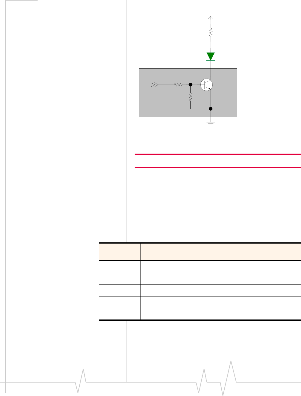
Host / Module Interfaces
Rev 1.9.1 Feb.09 Proprietary and Confidential 65
In the event of a discrepancy in values between this guide and the Product Specification Document (PSD), the PSD takes precedence.
Figure 5-1: Example LED
USIM interface
Note: This section applies only to GSM (MC87xx) modules.
ThemoduleisdesignedtosupportoneUSIM(Universal
SubscriberIdentityModule).TheUSIMholdsaccountinfor‐
mation,allowinguserstousetheiraccountonmultiple
devices.
TheUSIMinterfacehasfoursignals(plusGround).Theseare
definedinTable5‐3withanexamplecircuitshownin
Figure5‐2.(ForUSIMcardcontacts,seeFigure5‐3.)
Current limiting Resistor
LED
VCC 3.3V
MIO
MiniCard
Table 5-3: USIM pins
Pin name USIM contact
number Function
XIM_VCC 1USIM VCC
XIM_RESET 2Active low USIM reset
XIM_CLK 3Serial clock for USIM data
XIM_DATA 7Bi-directional USIM data line
XIM_GND 5Ground

CDMA and GSM / UMTS Mini Card Hardware Integration Guide
66 Proprietary and Confidential 2130114
In the event of a discrepancy in values between this guide and the Product Specification Document (PSD), the PSD takes precedence.
Figure 5-2: USIM application interface
Figure 5-3: USIM card contacts (contact view)
MC87xx
XIM_VCC
XIM_RESET
XIM_DATA
XIM_CLK
USIM card connector
GND
(Optional.
Locate near the
USIM socket)
47 pF, 51 Ω
4.7uF
X5R
typ
(C1)
XIM_VCC
XIM_CLK
XIM_IO
XIM_RESET
Located near
USIM socket
Located near USIM socket.
NOTE: Carefully consider if ESD
protection is required – it may
increase signal rise time and
lead to certification failure
GND
ESD
protection
(C3)
(C7)
(C2)
(C5)
(Optional.
Locate near the
USIM socket)
15 kΩ - 30 kΩ
C8
C7
C6
C5
C4
C3
C2
C1
GND VCC
VPP RST
I/O CLK
RFU RFU
Contact View (notched corner at top left)

Host / Module Interfaces
Rev 1.9.1 Feb.09 Proprietary and Confidential 67
In the event of a discrepancy in values between this guide and the Product Specification Document (PSD), the PSD takes precedence.
USIM operation
Note: For interface design
requirements, refer to:
(2G) 3GPP TS 51.010-1, section
27.17, or
(3G) ETSI TS 102 230 V5.5.0,
section 5.2
WhendesigningtheremoteUSIMinterface,youmustmake
surethattheUSIMsignalintegrityisnotcompromised.Some
designrecommendationsinclude:
•ThetotalimpedanceoftheVCCandGNDconnectionsto
theUSIM,measuredatthemoduleconnector,shouldbe
lessthan1Ωtominimizevoltagedrop(includesanytrace
impedanceandlumpedelementcomponents—inductors,
filters,etc.).
Note: The MC87xx is designed for use with either a 1.8 V or 3 V
USIM.
•PositiontheUSIMconnectornomorethan10cmfromthe
module.Ifalongerdistanceisrequiredbecauseofthe
designofthehostdevice,ashieldedwireassemblyis
recommended—connectoneendascloseaspossibletothe
USIMconnectorandtheotherendascloseaspossibleto
themoduleconnector.Theshieldedassemblymayhelp
shieldtheUSIMinterfacefromsystemnoise.
•ReducecrosstalkontheXIM_datalinetoreducetheriskof
failuresduringGCFapprovaltesting.
•AvoidroutingtheXIM_CLKandXIM_DATAlinesin
paralleloverdistancesgreaterthan2cm—cross‐couplingof
theselinescancausefailures.
•KeepUSIMsignalsasshortaspossible,andkeepverylow
capacitancetracesontheXIM_DATAandXIM_CLKsignals
tominimizesignalrisetime—signalrisetimemustbe<1μs.
Highcapacitanceincreasessignalrisetime,potentially
causingyourdevicetofailcertificationtests.
•Addexternalpull‐upresistors(15kΩ—30kΩ),ifrequired,
betweentheSIM_IOandSIM_VCClinestooptimizethe
signalrisetime.
•3GPPhasstringentrequirementsforI/Orisetime(<1μs),
signallevellimits,andnoiseimmunity—considerthis
carefullywhendevelopingyourPCBlayout.
•TheVCClineshouldbedecoupledclosetotheUSIM
socket.
•USIMisspecifiedtorunupto5MHz(USIMclockrate).
Takenoteofthisspeedintheplacementandroutingofthe
USIMsignalsandconnectors.
•Youmustdecideif,andhowmuch,additionalESD
protectionandseriesresistorsaresuitableforyourproduct.
TheMC87xxalreadyincludesadditionalESDprotection.
Addingmoreprotection(additionalcircuits)thanis
CDMA and GSM / UMTS Mini Card Hardware Integration Guide
68 Proprietary and Confidential 2130114
In the event of a discrepancy in values between this guide and the Product Specification Document (PSD), the PSD takes precedence.
necessarycoulddecreasesignalrisetime,increaseload
impedance,andcauseUSIMcertificationfailure.
•PuttinganoptionaldecouplingcapacitoratXIM_VCCnear
theUSIMsocketisrecommended—thelongerthetrace
length(impedance)fromthesockettothemodule,the
greaterthecapacitancerequirementtomeetcompliance
tests.
•Puttinganoptionalseriescapacitorandresistortermination
(toground)atXIM_CLKattheUSIMsockettoreduceEMI
andincreasesignalintegrityisrecommendedifthetrace
lengthbetweentheUSIMsocketandmoduleislong—47pF
and50Ωresistorarerecommended.
•ProtecttheUSIMsockettomakesurethattheUSIMcannot
beremovedwhilethemodule/hostdeviceispoweredup.
Forexample,youcouldplacethesocketunderthebattery
(forportabledevices);considersimilaroptionsforother
devicetypes.
•TestyourfirstprototypehosthardwarewithaComprion
IT3USIMtestdeviceatasuitabletestingfacility.
Extended AT commands
SeveralproprietaryATcommandsareavailableforthe
MC57xxandMC87xxtouseinhardwareintegrationdesign
andtesting(thesecommandsareNOTintendedforusebyend
users).RefertoCDMAExtendedATCommandReference
(Document2130621)fortheMC57xx,orMC87xxModem
ExtendedATCommandReference(Document2130616)forthe
MC87xxforalistofallavailablecommandsanddescriptions
oftheirfunctionality.
Someusefulcommandsforuseinhardwareintegrationare
listedinTable5‐4(MC57xx)andTable5‐5(MC87xx).
Table 5-4: MC57xx Extended AT commands
Command Description
Internal commands
!OEM Unlocks OEM protected commands
Modem state commands
!DIAG Sets diagnostic mode
!BOOTHOLD Resets modem and waits in boot loader
RF AT commands
!CHAN Sets RF band and channel

Host / Module Interfaces
Rev 1.9.1 Feb.09 Proprietary and Confidential 69
In the event of a discrepancy in values between this guide and the Product Specification Document (PSD), the PSD takes precedence.
!RX Turns on / off the first receiver
!RX2 Turns on / off the second receiver
!RXAGC Reads Rx AGC
!RX2AGC Reads second Rx AGC
!TX Enables Tx chain
!TXAGC Sets Tx AGC
!KEYON Turns on transmitter
!KEYOFF Turns off transmitter
!ALLUP Turns on transmitter in all ups condition
Provisioning commands
!CARRIERID Displays the carrier ID
CDMA commands
!STATUS Displays the status of the modem
!SCI Gets slot cycle index
Power control commands
!PCSTATE Power control state
!PCINFO Reads the power control information
!PCTEMP Reads the power control temperature
!PCVOLT Reads the power control voltage
Table 5-4: MC57xx Extended AT commands (Continued)
Command Description
Table 5-5: MC87xx Extended AT commands
Command Description
Password commands
!ENTERCND Enables access to password-protected
commands
!SETCND Sets AT command password
CDMA and GSM / UMTS Mini Card Hardware Integration Guide
70 Proprietary and Confidential 2130114
In the event of a discrepancy in values between this guide and the Product Specification Document (PSD), the PSD takes precedence.
Modem reset and status commands
!DTEMP Returns the temperature of the PA (Power
Amplifier) used by the:
•UMTS transceiver, or
•GSM transceiver
!GRESET Resets the modem
!GSTATUS Returns the operation status of the modem (mode,
band, channel, and so on)
Diagnostic commands
!BAND Selects a set of frequency bands or reports
current selection
!GBAND Reads / sets the current operating band
Test commands
!DAFTMACT
(password protected) Puts the modem into FTM (Factory Test Mode)
!DAFTMDEACT
(password-protected) Puts the modem into online mode
!DAGGRSSI
(password-protected) Returns the RSSI (Received Signal Strength
Indicator) in dBm (GSM mode)
!DAGGRSSIRAW
(password-protected) Returns the raw RSSI (GSM mode)
!DAGSLOCK
(password-protected) Returns the RF synthesizer lock state
!DAGSRXBURST
(password-protected) Sets the GSM receiver to burst mode
!DAGSRXCONT
(password-protected) Sets the GSM receiver continually on
!DAGSTXFRAME
(password-protected) Sets the GSM Tx frame structure
!DASBAND
(password-protected) Sets the frequency band (UMTS / GSM)
!DASCHAN
(password-protected) Sets the modem channel (frequency) (UMTS /
GSM)
!DASLNAGAIN
(password-protected) Sets the LNA (Low Noise Amplifier) gain state
!DASPDM
(password-protected) Sets the PDM (Pulse Duration Modulation) value
Table 5-5: MC87xx Extended AT commands (Continued)
Command Description

Host / Module Interfaces
Rev 1.9.1 Feb.09 Proprietary and Confidential 71
In the event of a discrepancy in values between this guide and the Product Specification Document (PSD), the PSD takes precedence.
!DASTXOFF
(password-protected) Turns off the Tx PA (Power Amplifier)
!DASTXON
(password-protected) Turns on the Tx PA (Power Amplifier)
!DAWGRXAGC
(password-protected) Returns the Rx AGC (Automatic Gain Control)
value (UMTS)
!DAWSCONFIGRX
(password-protected) Sets the UMTS receiver to factory calibration
settings
!DAWGCTON
(password-protected) Returns the Carrier to Noise ratio (WCDMA)
!DAWSPARANGE
(password-protected) Sets the PA range state machine (UMTS)
!DAWSTXCW
(password-protected) Sets the waveform used by the transmitter
(UMTS)
!OSDSM
(password-protected) Displays memory usage for DSM (Distributed
Shared Memory) buffer pools
Table 5-5: MC87xx Extended AT commands (Continued)
Command Description

CDMA and GSM / UMTS Mini Card Hardware Integration Guide
72 Proprietary and Confidential 2130114
In the event of a discrepancy in values between this guide and the Product Specification Document (PSD), the PSD takes precedence.

6
Rev 1.9.1 Feb.09 Proprietary and Confidential 73
In the event of a discrepancy in values between this guide and the Product Specification Document (PSD), the PSD takes precedence.
6: Thermal Considerations
Thischapterdescribesthethermalcharacteristicsofthe
moduleandprovidessuggestionsfortestingandaddressing
thermalissues.
Thermal considerations
MiniCardscangeneratesignificantamountsofheatthatmust
bedissipatedinthehostdeviceforsafetyandperformance
reasons.
Theamountofthermaldissipationrequireddependsonthe
followingfactors:
•Supplyvoltage—Maximumpowerdissipationforthese
modulescanbeupto3.1Watvoltagesupplylimits.
•Usage—Typicalpowerdissipationvaluesdependonthe
locationwithinthehost,amountofdatatransferred,etc.
Specificareasrequiringheatdissipationincludethefourshield
casesindicatedinFigure6‐1.
•Transmitter—topshield(nexttoRFconnectors).Thisis
likelytobethehottestarea.
•Baseband1—bottomshield,belowthetransmitter
•Receiver—topshield,othersideofmodulefromthetrans‐
mitter
•Baseband2—bottomshield,belowthereceiver
Youcanenhanceheatdissipationby:
•Maximizingairflowover/aroundthemodule
•Locatingthemoduleawayfromotherhotcomponents
Note: Adequate dissipation of heat is necessary to ensure that the
module functions properly, and to comply with the thermal require-
ments in PCI Express Mini Card Electromechanical Specification
Revision 1.1.
Module testing
Whentestingyourintegrationdesign:
•Testtoyourworstcaseoperatingenvironmentconditions
(temperatureandvoltage)
•Testusingworstcaseoperation(transmitteron100%duty
cycle,maximumpower)
•Monitortemperatureatallshieldlocations.Attachthermo‐
couplestoeachshieldindicatedbelow
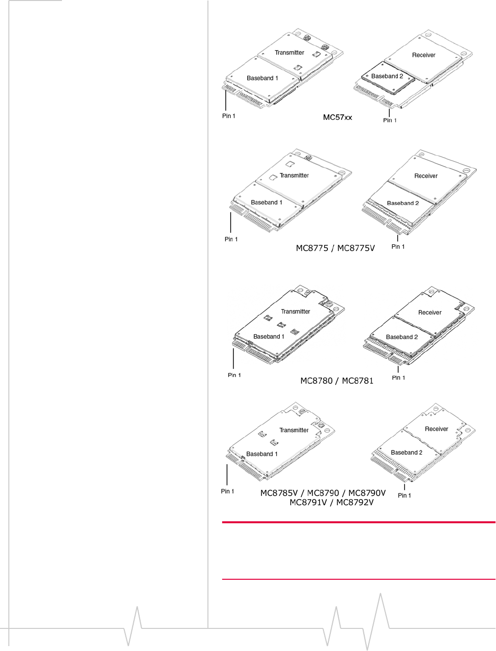
CDMA and GSM / UMTS Mini Card Hardware Integration Guide
74 Proprietary and Confidential 2130114
In the event of a discrepancy in values between this guide and the Product Specification Document (PSD), the PSD takes precedence.
Figure 6-1: Shield locations
Note: Make sure that your system design provides sufficient cooling
for the module. The RF shield temperature should be kept below
90 °C when integrated to prevent damage to the module’s compo-
nents.
7
Rev 1.9.1 Feb.09 Proprietary and Confidential 75
In the event of a discrepancy in values between this guide and the Product Specification Document (PSD), the PSD takes precedence.
7: Design Checklist
Thischapterprovidesasummaryofthedesignconsiderations
mentionedthroughoutthisguide.Thisincludesitemsrelating
tothepowerinterface,RFintegration,thermalconsiderations,
cablingissues,andsoon.
Note: This is NOT an exhaustive list of design considerations. It is
expected that you will employ good design practices and engineering
principles in your integration.
Table 7-1: Hardware integration design considerations
Suggestion Section where discussed
Component placement
Protect the USIM socket so that the USIM cannot be removed
while the host is powered up.
USIM operation
page 67
If an ESD suppressor is not used, allow space on the USIM
connector for series resistors in layout (up to 100 Ω may be used
depending on ESD testing requirements).
USIM operation
page 67
Minimize RF cable losses as these affect the performance values
listed in the product specification document.
RF connection
page 39
Antennas
Match the module / antenna coax connections to 50 Ω —
mismatched antenna impedance and cable loss negatively
affects RF performance.
RF connection
page 39
If installing both the MC57xx and MC87xx in the same device,
consider using separate antennas for maximum performance.
Antenna and cabling
page 40
Power
Limit host power rail dips caused by module inrush current by
adding sufficient capacitance to the host power rail.
Inrush currents
page 24
Make sure the power supply can handle the maximum current
specified for the module type.
Current consumption overview
page 27
Limit the total impedance of VCC and GND connections to the
USIM at the connector to less than 1 Ω (including any trace
impedance and lumped element components — inductors,
filters, etc.). All other lines must have a trace impedance less
than 2 Ω.
USIM operation
page 67

CDMA and GSM / UMTS Mini Card Hardware Integration Guide
76 Proprietary and Confidential 2130114
In the event of a discrepancy in values between this guide and the Product Specification Document (PSD), the PSD takes precedence.
Decouple the VCC line close to the USIM socket. The longer the
trace length (impedance) from socket to module, the greater the
capacitance requirement to meet compliance tests.
USIM operation
page 67
EMI / ESD
Investigate sources of localized interference early in the design
cycle.
Methods to mitigate decreased
Rx performance
page 42
Provide ESD protection for the USIM connector at the exposed
contact point (in particular, the CLK, VCC, IO, and RESET lines).
USIM operation
page 67
Keep very low capacitance traces on the XIM_DATA and
XIM_CLK signals.
To minimize noise leakage, establish a very good ground
connection between the module and host.
Ground connection
page 39
Route cables away from noise sources (for example, power
supplies, LCD assemblies, etc.).
Methods to mitigate decreased
Rx performance
page 42
Shield high RF-emitting components of the host device (for
example, main processor, parallel bus, etc.).
Methods to mitigate decreased
Rx performance
page 42
Use discrete filtering on low frequency lines to filter out unwanted
high-order harmonic energy.
Methods to mitigate decreased
Rx performance
page 42
Use multi-layer PCBs to form shielding layers around high-speed
clock traces.
Methods to mitigate decreased
Rx performance
page 42
Thermal
Test to worst case operating conditions — temperature, voltage,
and operation mode (transmitter on 100% duty cycle, maximum
power).
Thermal considerations
page 73
Use appropriate techniques to reduce module temperatures.
(airflow, heat sinks, heat-relief tape, module placement, etc.)
Thermal considerations
page 73
Host / Modem communication
Make sure the host USB driver supports remote wakeup,
resume, and suspend operations, and serial port emulation.
USB handshaking
page 62
When no valid data is being sent, do not send SOF tokens from
the host (causes unnecessary power consumption).
USB handshaking
page 62
Table 7-1: Hardware integration design considerations (Continued)
Suggestion Section where discussed

8
Rev 1.9.1 Feb.09 Proprietary and Confidential 77
In the event of a discrepancy in values between this guide and the Product Specification Document (PSD), the PSD takes precedence.
8: Testing
Note: All Sierra Wireless embedded modules are factory-tested to
ensure they conform to published product specifications.
DevelopersofOEMdevicesintegratingSierraWireless
modulesshouldincludeaseriesoftestphasesintheir
manufacturingprocesstomakesurethattheirdeviceswork
properlywiththeembeddedmodules.
Suggestedphasesinclude:
•Acceptance testing—testingofmoduleswhentheyare
receivedfromSierraWireless
•Certification testing—testingofcompleteddevicestoobtain
requiredcertificationsbeforebeginningmassproduction
•Production testing—testingofcompleteddeviceswiththe
modulesembedded
•Quality assurance testing—post‐production
AT command entry timing requirement
Somecommandsrequiretimetoprocessbeforeadditional
commandsareentered.Forexample,themodemwillreturn
“OK”whenitreceivesAT!DAFTMACT.IfAT!DASBANDis
receivedtoosoonafterthis,themodemwillreturnanerror.
Whenbuildingautomatedtestscripts,ensurethatsufficient
delaysareembeddedwherenecessarytoavoidtheseerrors.
Acceptance testing
Note: Acceptance testing is
typically performed for each
shipment received.
WhenyoureceiveashipmentfromSierraWireless,youshould
makesureitissuitablebeforebeginningproduction.
Fromarandomsamplingofunits,testthat:
•Theunitsareoperational
•Theunitsareloadedwiththecorrectfirmwareversion
Test requirements
Toperformthesuggestedtests,yourequireatestsystemin
whichtotemporarilyinstallthemodule,andyoumustbeable
toobservethetestdevice’sLEDindicator.

CDMA and GSM / UMTS Mini Card Hardware Integration Guide
78 Proprietary and Confidential 2130114
In the event of a discrepancy in values between this guide and the Product Specification Document (PSD), the PSD takes precedence.
Te s t p r o c e d u r e
Thefollowingisasuggestedacceptancetestingprocedure
usingSierraWireless’Watchersoftware:
Note: You can perform these
tests using appropriate AT
commands.
Test 1: Check power-up and initialization
1. Afterinstallingthemodule,startthetestsystem.
2. LaunchWatcher.
3. ChecktheLED—iftheLEDisoff,thereisaproblemwith
themoduleorwiththeconnectiontotheLED.
Test 2: Check version numbers
1. FromWatcher,selectHelp > About.
2. VerifythatthefirmwareversionintheAboutwindowis
correct.
3. ClosetheAboutwindow.
Ifthemodulefailseitherofthesetests,orisnotrecognizedby
Watcher:
1. Replacethemodulewithonethatisknowntowork
correctlyandrepeatthetests.
2. Ifthetestsaresuccessful,reinstalltheoriginalmoduleand
repeatthetests.
Ifthemodulestilldoesnotworkcorrectly,contactyour
accountmanager.
Certification testing
Note: Typically, you need to
pass certification testing of your
device with the integrated
module one time only.
WhenyouproduceahostdevicewithanembeddedSierra
Wirelessmodule,youmustobtaincertificationsforthefinal
productfromappropriateregulatorybodiesinthejurisdic‐
tionswhereitwillbedistributed.
Note: The module itself (MC57xx, MC87xx) has been certified
already—only the integrated device needs certification.
Thefollowingaresomeoftheregulatorybodiesfromwhich
youmayrequirecertification—itisyourresponsibilitytomake
surethatyouobtainallnecessarycertificationsforyour
productfromtheseorothergroups:
•FCC(FederalCommunicationsCommission—www.fcc.gov)
•IndustryCanada(www.ic.gc.ca)
•CSA(CanadianStandardsAssociation—www.csa.ca)
•FactoryMutual(FMGlobal—www.allendale.com)

Testing
Rev 1.9.1 Feb.09 Proprietary and Confidential 79
In the event of a discrepancy in values between this guide and the Product Specification Document (PSD), the PSD takes precedence.
•UnderwritersLaboratoriesInc.(www.ul.com)
•(MC57xxonly)CDG(CDMADevelopmentGroup—
www.cdg.org)
•(MC87xxonly)GCF(GlobalCertificationForum—
gcf.gsm.org)outsideofNorthAmerica
•(MC87xxonly)PTCRB(PCSTypeCertificationReview
Board—www.ptcrb.com)inNorthAmerica
Production testing
Note: Production testing
typically continues for the life of
the product.
Eachassembleddeviceshouldbetestedtomakesurethe
moduleisinstalledcorrectlyandisfunctioningwithinnormal
operatingparameters.
Note: All Sierra Wireless embedded modules are fully factory-tested
to ensure they conform to published product specifications.
Ingeneral,productiontestingensuresthatthemoduleis
installedcorrectly(I/Osignalsarepassedbetweenthehostand
module),andtheantennaisconnectedandperformingto
specifications(RFtests).
Typicalitemstotestincludehostconnectivity,theRFassembly
(Txand/orRx,asappropriate),andtheaudioassembly(for
voice‐enabledmodules).
Note: The amount and types of tests to perform are your decision—
the tests listed in this section are guidelines only. Make sure that the
tests you perform exercise functionality to the degree that your
situation requires—this may include, for example, testing network
availability, any host device configuration issues, baseband testing
(GPIO / Audio, host / module connectors) and appropriate RF testing
(Tx and/or Rx).
Useanappropriateteststationforyourtestingenvironment
(seeTest requirementsonpage77forsuggestions)anduseAT
commandstocontroltheintegratedmodule.
Note: Your test location must be protected from ESD to avoid inter-
ference with the module and antenna(s) (assuming that your test
computer is in a disassembled state).
Also, consider using an RF shielding box as shown in the suggested
test equipment—local government regulations may prohibit
unauthorized transmissions.

CDMA and GSM / UMTS Mini Card Hardware Integration Guide
80 Proprietary and Confidential 2130114
In the event of a discrepancy in values between this guide and the Product Specification Document (PSD), the PSD takes precedence.
Suggested manual functional
test procedure
Thissectionpresentsaprocedureforperformingabasic
manualfunctionaltestonalaboratorybenchusingtheMini
CardandaMiniCardDevKit.Whenyouhavebecome
familiarwiththetestingmethod,useittodevelopyourown
automatedproductiontestingprocedures.
Suggested tests
Considerthefollowingtestswhenyoudesignyourproduction
testproceduresfordeviceswiththeMC57xxand/orMC87xx
installed.
•Visualcheckofthemodule’sconnectors,RFassemblies,and
audioassemblies(ifapplicable)
•Moduleisoperational
•USBconnectionisfunctional
•LEDisfunctional
•W_Disable#(modulepowerdown)
•Firmwarerevisioncheck
•Rxtestsonmainandauxiliarypaths
•Txtest
•Audio(microphoneandspeaker)tests(forvoice‐enabled
modules)
Suggested test plan procedure
Note: The following is a suggested outline for a relatively compre-
hensive test plan—you must decide which tests are appropriate for
your product.
This is not an exhaustive list of tests—you may wish to add additional
tests that more fully exercise the capabilities of your product.
Note: You may choose to create and run a test program that
automates portions of the test procedure.
UsinganappropriateDevKit‐basedteststation(asuggested
setupisdescribedinSuggested testing equipmentonpage97),
andreferringtotheappropriatestandardandextendedAT
commandreferences:
1. Visuallyinspectthemodule’sconnectorsandRFassem‐
bliesforobviousdefectsbeforeinstallingitinthetest
station.
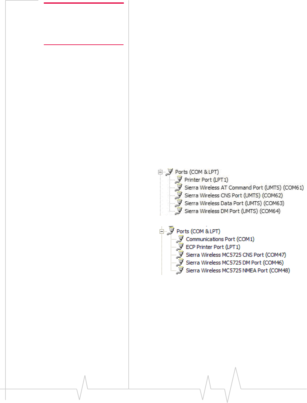
Testing
Rev 1.9.1 Feb.09 Proprietary and Confidential 81
In the event of a discrepancy in values between this guide and the Product Specification Document (PSD), the PSD takes precedence.
Note: To power-off the module,
drive W_Disable# low for the
required minimum period. See
State change: Power off / on on
page 23 for details.
2. Ensurethatthemoduleisturnedoffbeforebeginning
yourtests(setW_Disable#low).
3. IfusingLinux,determineifanyUSBdevicesarecurrently
connectedtothecomputer:
a. Openashellwindowandenterthecommandls /dev/
tty/USB*.
b. RecordthettyUSBnvaluesthatarereturned;theseare
thecurrentlyconnectedUSBdevices.Ifthecommand
returns“nosuchfileordirectory”,therearenodevices
currentlyconnected.
4. TestW_Disable#—Turnonthemodulebyletting
W_Disable#float(highimpedance).Dependingonyour
device,thismayjustrequirepoweringupthedevice.Refer
tothePCIExpressMiniCardDevKitQuickStartGuide
(Document2130705)formoredetails.
5. TestUSBfunctionality—CheckforUSBenumeration.
·(Windowssystems)TheDeviceManagershowsSierra
WirelessitemsunderthePorts‐(COM&LPT)entry.The
devicesshowndependonthemoduletype.For
example:
·MC87xx
·MC57xx
·(Linuxsystems)Enterthecommandls /dev/tty/USB*and
thenrecordandcomparetheresultswiththosefrom
Step3.IfthereareanynewttyUSBndevices,thenthe
modemhasenumeratedsuccessfully.(Thereshouldbe
threeorsevennewdevices,dependingonthemodule
type.)Forexample:

CDMA and GSM / UMTS Mini Card Hardware Integration Guide
82 Proprietary and Confidential 2130114
In the event of a discrepancy in values between this guide and the Product Specification Document (PSD), the PSD takes precedence.
·MC5725/MC5725V/MC8775/MC8775V/MC8780/
MC8781(withnootherUSBdevicesconnected):
(TheATportisthethirdnewenumerateddevice—/
dev/ttyUSB2.)
·MC5727/MC5727V/MC5728V/MC8785V/MC8790/
MC8790V/MC8791V/MC8792V(withoneotherUSB
devicealreadyconnectedandassignedtottyUSB1):
(TheATportisthefourthnewenumerateddevice—/
dev/ttyUSB4.)
6. SomemodulescauseaSierraWirelessNetworkAdapterto
appearinDeviceManager,asshownbelow.Disablethe
adaptertoallowentryofATcommandswhenperforming
diagnostictests.
a. Right‐clicktheSierraWirelessNetworkAdapterto
displaythecontextmenu.
b. ClickDisable.
MC57xx
7. Makesureyourmodemisconnectedandrunning,and
thenestablishcontactwiththemodule:
(Windowssystems)
Useaterminalemulation/communicationsprogramsuch
asMicrosoftHyperTerminal®toconnectovertheCOM
portreservedforATcommands(seelistingsinStep5):
a. StartHyperTerminal.
b. OntheFilemenu,selectConnectionDescription.The
ConnectionDescriptiondialogboxappears.

Testing
Rev 1.9.1 Feb.09 Proprietary and Confidential 83
In the event of a discrepancy in values between this guide and the Product Specification Document (PSD), the PSD takes precedence.
c. Type“Sierra”intheNameboxandclickOK.The
ConnectTodialogboxappears.
d. ClickOKwithoutchanginganyofthedisplayedinfor‐
mation.TheConnectdialogboxappears.
e. ClickCancel.
Note: If necessary, use AT E1 to
enable echo.
f. TypeATZintheHyperTerminalwindow.Ifthe
connectionisestablished,themessageOKappears.
(Linuxsystems)
Useaterminalemulation/communicationsprogramsuch
asminicomtoconnectoverthedevicehandleforATcom‐
mands(seelistingsinStep5):
Note: If the command “minicom”
is not found, then use a different
program, or download minicom
and repeat this step. See
“Downloading and configuring
minicom for Linux systems” on
page 84 for details.
a. Startminicom:
·Firstuseofthemodem:Fromthecommandline,type
minicom‐s.‐‐alwaysshowsconfigurationmenu
·Subsequentuses:Fromthecommandline,type
minicom.
Theminicomconfigurationdetailsappearandthe
messageOKappearswhentheconnectionisestab‐
lished.
8. Displaythefirmwareversionusingthiscommand:
·MC57xx:AT+GMR
·MC87xx:AT!GVER
Exampleresponse:
·p2005000,0 [Aug 09, 2006 14:28:24],, VID: PID:
Characters5–6arethefirmwareversion(50inthisexam‐
ple).
9. TesttheLED—SettheLEDinblinkingmodeusingthis
command,thenvisuallyverifythattheLEDturnsoffand
on:
·MC57xx:AT!LED=0,1
·MC87xx:AT!DLEDorAT!LEDCTRL
10. UnlocktheextendedATcommandset,using:
·MC57xx:AT!OEM=176
·MC87xx:AT!ENTERCND

CDMA and GSM / UMTS Mini Card Hardware Integration Guide
84 Proprietary and Confidential 2130114
In the event of a discrepancy in values between this guide and the Product Specification Document (PSD), the PSD takes precedence.
11. Putthemoduleindiagnostic/factorytestmodeusing:
·MC57xx:AT!DIAG
·MC87xx:AT!DAFTMACT
12. (MC87xxonly)CommunicatewiththeUSIMusing+CPIN
or+CIMI.
Note: When performing RF
tests, use a test platform similar
to those shown in Figure 8-2
(page 98) and Figure 8-3
(page 99).
13. TestRFtransmission,ifdesired:
·MC57xx—SeeTestingRFtransmissionpath—MC57xx
onpage85.
·MC87xx—SeeTestingRFtransmissionpath—MC87xx
onpage86.
14. TestRFreception,ifdesired:
·MC57xx—SeeTestingRFReceivepath—MC57xxon
page88.
·MC87xx—SeeTestingRFReceivepath—MC87xxon
page90.
Note: The GPS receiver does
not need to be tested for UMTS
(MC878x) or CDMA (MC57xx)
modules supporting diversity
because RF connectivity is
validated by testing the diversity
receiver in Step 14.
15. (MC8775Vonly)TesttheGPSreceiver,ifdesired.See
TestingGPSReceiver—MC8775Vonpage93.
16. TestAudioloop‐back.SeeTestAudioLoop‐back—
MC5725V/MC5727V/MC5728V/MC8775V/MC8785V/
MC8790V/MC8791V/MC8792Vonpage94.
17. Finishtesting
a. IfthenetworkadapterwasdisabledinStep6,re‐
enableit(sameinstructions,exceptclickEnable
insteadofDisable).
Note: To power-off the module,
drive W_Disable# low for the
required minimum period. See
State change: Power off / on on
page 23 for details.
b. SettheW_Disable#signallowandconfirmthatthe
modulepowersdown:
·Windowssystems—TheSierraWirelessitemsunder
thePorts(COM&LPT)entryinDeviceManager
disappearasthemodulepowersoff.
·Linuxsystems—Enterthecommandls /dev/tty/USB*.
ThedevicesenumeratedinStep5willnotappearafter
themodulepowersoff.
Downloading and configuring minicom for Linux systems
Note: This procedure is for Ubuntu systems. If you are using a
different Linux distribution, use the appropriate commands for your
system to download minicom.
TodownloadandconfigureminicominaUbuntusystem:
Note: To install minicom, you
must have root access, or be
included in the sudoers list.
1. Downloadandinstallminicom—enterthefollowing
command:
sudo apt-get install minicom
Testing
Rev 1.9.1 Feb.09 Proprietary and Confidential 85
In the event of a discrepancy in values between this guide and the Product Specification Document (PSD), the PSD takes precedence.
2. Whenprompted,enteryouruserpasswordtobeginthe
downloadandinstallation.Whenminicomisinstalled,the
shellpromptappears.
3. Configureminicomtocommunicatewithyourmodem:
a. Startminicomwiththefollowingcommand:
minicom -s
4. Usethedown‐arrowkeytoselectthe“Serialportsetup”
option.
5. RefertoStep5onpage81toidentifythedevicefilehandle
(/dev/ttyUSBn)touseforATcommands.
6. IndicatethefilehandletouseforATcommands—enterA
andthenreplacetheserialdevicestringwiththeATfile
handle(forexample,/dev/ttyUSB4foranMC8792Vas
shownintheexampleinStep5onpage81).
7. PressEntertwice.
8. Usethedown‐arrowkeytoselectSave setup as dfl.
9. SelectExit.
Testing RF transmission path—MC57xx
Note: This procedure segment is performed in Step 13 of the
Suggested test plan procedure (page 84).
TotesttheDUT’stransmitterpath:
Note: This procedure describes
steps using the "Power Meter:
Gigatronics 8651A” (with Option
12 and Power Sensor 80701A).
1. Setupthepowermeter:
a. Makesurethemeterhasbeengivensufficienttimeto
warmup,ifnecessary,toenableittotakeaccurate
measurements.
b. Zero‐calibratethemeter.
c. EnableMAPmode.

CDMA and GSM / UMTS Mini Card Hardware Integration Guide
86 Proprietary and Confidential 2130114
In the event of a discrepancy in values between this guide and the Product Specification Document (PSD), the PSD takes precedence.
Note: These AT commands
generate a modulated test
signal.
2. PreparetheDUTusingthefollowingATcommands:
a. AT!OEM=176 (UnlockstheextendedATcommand
set)
b. AT!DIAG (Setmodemindiagnosticmode)
c. AT!CHAN=600,1 (PCSband,channel600)
or
AT!CHAN=384,0 (Cellularband,channel384)
Thepowermetershouldread‐100dBm,indicatingno
signal.
d. AT!TX=1 (Turnsontransmitter)
e. AT!ALLUP=1 (Enablesallupscondition)
Thepowermetershouldreadfrom0–24dBm,
dependingonyoursetup.
f. AT!TX=0 (Turnsofftransmitter)
3. Testlimits:
RuntenormoregoodDUTsthroughthistestproce‐
duretoobtainanominaloutputpowervalue.
·Applyatoleranceof±5to6dBtoeachmeasurement
(assumingagoodsetupdesign).
·Monitortheselimitsduringmass‐productionramp‐up
todetermineiffurtheradjustmentsareneeded.
Note: The MC57xx has a nominal output power of +24 dBm
±
1 dB.
However, the value measured by the power meter depends on the
test setup (RF cable loss, couplers, splitters) and the DUT design.
Note: When doing the same test over the air in an RF chamber,
values are likely to be significantly lower.
Testing RF transmission path—MC87xx
Note: This procedure segment is performed in Step 13 of the
Suggested test plan procedure (page 84).
Table8‐1containsparametersusedinthesuggestedtest
procedurethatfollows.
Testing
Rev 1.9.1 Feb.09 Proprietary and Confidential 87
In the event of a discrepancy in values between this guide and the Product Specification Document (PSD), the PSD takes precedence.
TotesttheDUT’stransmitterpath:
Note: This procedure describes
steps using the "Power Meter:
Gigatronics 8651A” (with Option
12 and Power Sensor 80701A).
1. Setupthepowermeter:
a. Makesurethemeterhasbeengivensufficienttimeto
warmup,ifnecessary,toenableittotakeaccurate
measurements.
b. Zero‐calibratethemeter.
c. EnableMAPmode.
2. PreparetheDUTusingthefollowingATcommands:
a. AT!UNLOCK=”<lockCode>” (UnlocksextendedAT
commandset)
or
AT!ENTERCND
b. AT!DAFTMACT (Enterstestmode)
c. AT!DASBAND=<bandValue>
·SeeTable8‐1forappropriate<bandValue>values
d. AT!DASCHAN=<channel>
·SeeTable8‐1forappropriate<channel>values
e. (GSMmodeonly)
AT!DAGSTXFRAME=0, 1, 3000, 0
f. AT!DASTXON (Turnsonthetransmitpath)
g. (WCDMAmodeonly)
AT!DAWSTXCW=0(Useamodulatedcarrier)
Table 8-1: Test settings for MC87xx transmission path testing
Bands
Mode Test category 850 900 1800 1900 2100
WCDMA Band 22 29 15 9
Channel 4182 2812 9400 9750
GSM Band 18 10 11 12
Channel 190 65 697 661

CDMA and GSM / UMTS Mini Card Hardware Integration Guide
88 Proprietary and Confidential 2130114
In the event of a discrepancy in values between this guide and the Product Specification Document (PSD), the PSD takes precedence.
h. (WCDMAmodeonly)
AT!DASPDM=2, 455 (Setthepowerlevel,tunable
from0to511)
i. (WCDMAmodeonly)
AT!DAWSPARANGE=3(SettohighPAgainstate)
j. Takethemeasurement.
k. AT!DASTXOFF (Turnsoffthetransmitter)
3. Testlimits:
RuntenormoregoodDUTsthroughthistestproce‐
duretoobtainanominaloutputpowervalue.
·Applyatoleranceof±5to6dBtoeachmeasurement
(assumingagoodsetupdesign).
·Monitortheselimitsduringmass‐productionramp‐up
todetermineiffurtheradjustmentsareneeded.
·ForGSMmode,thetransmitsignalisbursted,sothe
transmitpowerwillappearaveragedonthepower
meterreading.
Note: The MC87xx has a nominal output power of +23 dBm
±
1 dB in
WCDMA mode. However, the value measured by the power meter is
significantly influenced (beyond the stated
±
1 dB output power
tolerance) by the test setup (host RF cabling loss, antenna efficiency
and pattern, test antenna efficiency and pattern, and choice of shield
box).
Note: When doing the same test over the air in an RF chamber,
values are likely to be significantly lower.
Testing RF Receive path—MC57xx
Note: This procedure segment is performed in Step 14 of the
Suggested test plan procedure (page 84).
TotesttheDUT’sreceivepath:
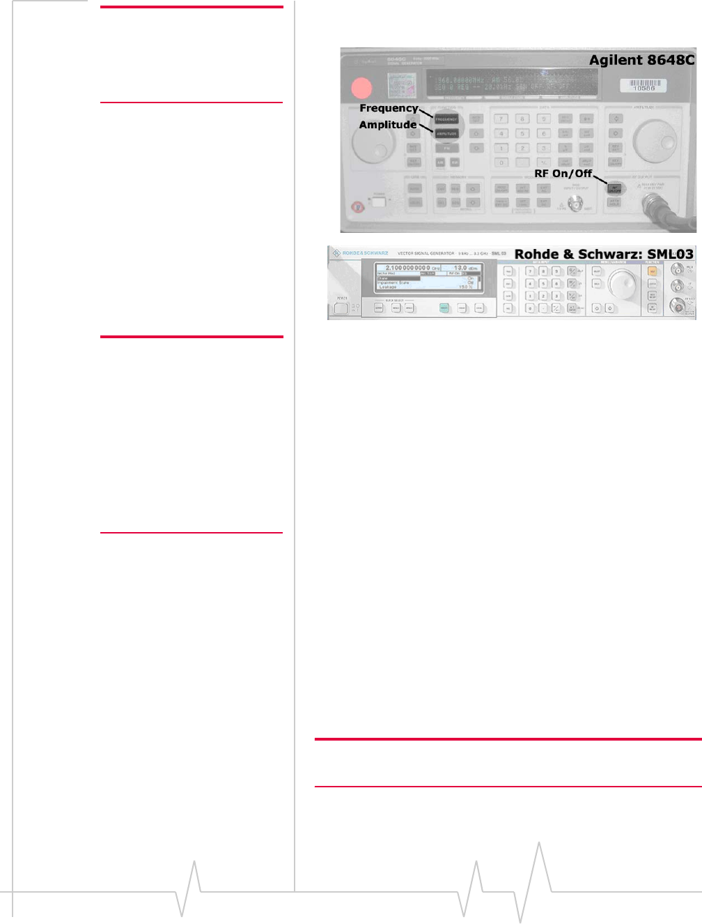
Testing
Rev 1.9.1 Feb.09 Proprietary and Confidential 89
In the event of a discrepancy in values between this guide and the Product Specification Document (PSD), the PSD takes precedence.
Note: This procedure describes
steps using the Agilent 8648C
signal generator—the Rohde &
Schwarz SML03 is shown for
reference only.
1. Setupthesignalgenerator:
Note: This example setup uses
a 200 kHz offset from band
center for testing using a
continuous wave—you can use
any appropriate baseband
frequency offset (for example,
100 kHz, 300 kHz, etc.).
If using a modulated signal, set
the frequency to band center
with no offset.
a. PresstheFrequencybuttontosetthefrequencyto
1960.200MHzforPCSband,Channel600,or
881.720MHzforCellularband,Channel384
b. PresstheAmplitudebuttontosettheamplitudeto
‐55.0dBm.
c. PresstheRFON/OFFbuttontoenableordisablethe
RFportofthesignalgenerator.
2. Readbackthepowerlevelfromthemainreceiver:
a. AT!OEM=176(UnlockstheextendedATcommandset)
b. AT!DIAG(SetsthemodeminDiagnosticmode)
c. AT!CHAN=600,1 (PCSband,channel600)
or
AT!CHAN=384,0(Cellularband,channel384)
d. AT!RX=1(Turnsonthemainreceiver)
e. AT!RXAGC?(Readsbackthepowerlevel,indBm,from
themainreceiver)
Responseexamples:
·RXAGC=0xFFFFFF33=‐77dBm(whensignal
generator’sRFportisOFF)
·RXAGC=0x0021=‐60dBm(whensignalgenerator’s
RFportisON)typical
Note: The dBm value displayed is calculated to reflect the power at
the input connector.
f. AT!RX2=1 (Turnsondiversityreceiver)

CDMA and GSM / UMTS Mini Card Hardware Integration Guide
90 Proprietary and Confidential 2130114
In the event of a discrepancy in values between this guide and the Product Specification Document (PSD), the PSD takes precedence.
g. AT!RX2AGC?(Readsbackthepowerlevel,indBm,
fromthediversityreceiver)
Responseexamples:
·RX2AGC=0xFFFFFF76=‐84dBm(whensignal
generator’sRFportisOFF)
·RX2AGC=0xFFFFFFC6=‐69dBm(whensignal
generator’sRFportisON)typical
h. AT!RX=0(Turnsoffmainreceiver)
i. AT!RX2=0(Turnsoffdiversityreceiver)
3. Testlimits
RuntenormoregoodDUTsthroughthistestproce‐
duretoobtainanominalreceivedpowervalue.
·Applyatoleranceof±5to6dBtoeachmeasurement
(assumingagoodsetupdesign).
·Makesurethemeasurementismadeatahighenough
levelthatitisnotinfluencedbyDUT‐generatedand
ambientnoise.
·TheSignalGeneratorpowerlevelshouldbeatleast
‐50dBm.
·Monitortheselimitsduringmass‐productionramp‐up
todetermineiffurtheradjustmentsareneeded.
Note: The value measured by the DUT depends on the test setup and
DUT design. Host RF cabling loss, antenna efficiency and pattern,
test antenna efficiency and pattern, and choice of shield box all signifi-
cantly influence the measurement.
Note: When doing the same test over the air in an RF chamber,
values are likely to be significantly lower.
Testing RF Receive path—MC87xx
Note: This procedure segment is performed in Step 14 of the
Suggested test plan procedure (page 84).
Table8‐2containsparametersusedinthesuggestedtest
procedurethatfollows.
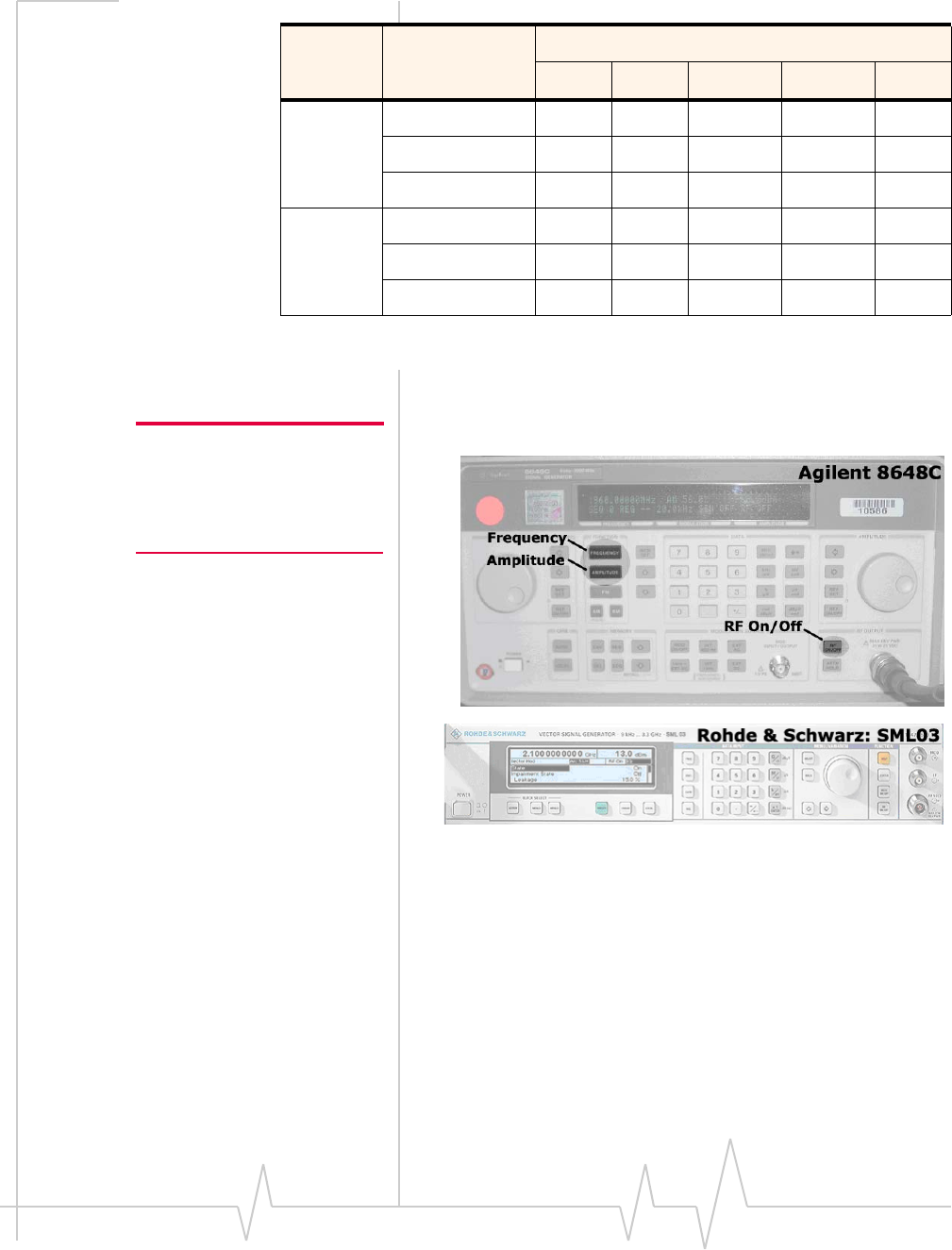
Testing
Rev 1.9.1 Feb.09 Proprietary and Confidential 91
In the event of a discrepancy in values between this guide and the Product Specification Document (PSD), the PSD takes precedence.
TotesttheDUT’sreceivepath:
Note: This procedure describes
steps using the Agilent 8648C
signal generator—the Rohde &
Schwarz SML03 is shown for
reference only.
1. Setupthesignalgenerator:
a. Settheamplitudeto:
·‐80dBm(WCDMAmode)
·‐60dBm(GSMmode)
b. Setthefrequencyforthebandbeingtested.See
Table8‐2forfrequencyvalues.
2. SetuptheDUT:
a. AT!UNLOCK=”<customerCode>”orAT!ENTERCND
b. AT!DAFTMACT
c. AT!DASBAND=<band>
·SeeTable8‐2for<band>values
d. AT!DASCHAN=<channel>
Table 8-2: Test settings for MC87xx Receive path testing
Bands
Mode Test category 850 900 1800 1900 2100
WCDMA Frequency1(MHz) 882.60 948.60 1961.2 2141.2
Band 22 29 15 9
Channel 4182 2812 9400 9750
GSM Frequency2(MHz) 881.667 948.067 1842.267 1960.067
Band 18 10 11 12
Channel 190 65 697 661
1 All values offset from actual center channel by +1.2 MHz
2 All values offset from actual center channel by +67 kHz

CDMA and GSM / UMTS Mini Card Hardware Integration Guide
92 Proprietary and Confidential 2130114
In the event of a discrepancy in values between this guide and the Product Specification Document (PSD), the PSD takes precedence.
·SeeTable8‐2for<channel>values
e. AT!DASLNAGAIN=0(setstheLNAtomaximumgain)
f. (WCDMAmode)
i. AT!DAWGAVGAGC=9400,0(forPCS1900,channel
9400asanexample)
(GSMmode)
i. AT!DAGSRXBURST=0 (settoreceiveburstedmode)
ii. AT!DAGGAVGRSSI=190,0 (forchannel190,for
example)
ThereturnedvalueistheRSSIindBm.
3. Testlimits:
RuntenormoregoodDUTsthroughthistestproce‐
duretoobtainanominalreceivedpowervalue.
·Applyatoleranceof±5to6dBtoeachmeasurement
(assumingagoodsetupdesign).
·Makesurethemeasurementismadeatahighenough
levelthatitisnotinfluencedbyDUT‐generatedand
ambientnoise.
·TheSignalGeneratorpowerlevelcanbeadjustedand
newlimitsfoundiftheradiatedtestneedsgreater
signalstrength.
·Monitortheselimitsduringmass‐productionramp‐up
todetermineiffurtheradjustmentsareneeded.
Note: The value measured from the DUT is significantly influenced by
the test setup and DUT design (host RF cabling loss, antenna
efficiency and pattern, test antenna efficiency and pattern, and choice
of shield box).
Note: Diversity is not available in
GSM mode.
4. TestdiversitypathsfortheMC8780(WCDMA850/
WCDMA2100),MC8781(WCDMA850/WCDMA1900),
orMC8785V/MC8790/MC8790V(WCDMA850/
WCDMA1900/WCDMA2100):
a. SetupthesignalgeneratorasinStep1.
b. SetuptheDUT:
Note: Setup of the DUT is the
same as in Step 2, except for a
change to AT!DAWGAVGAGC
and the addition of
AT!DAWSSCHAIN.
i. AT!UNLOCK=”<customerCode>”orAT!ENTERCND
ii. AT!DAFTMACT
iii. AT!DASBAND=<band>
·SeeTable8‐2for<band>values
iv. AT!DAWSSCHAIN=1(enablesthesecondarychain)
v. AT!DASCHAN=<channel>
·SeeTable8‐2for<channel>values
vi. AT!DASLNAGAIN=0(setstheLNAtomaximumgain)
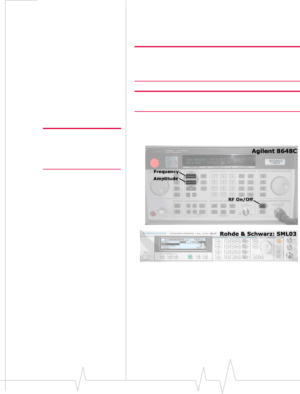
Testing
Rev 1.9.1 Feb.09 Proprietary and Confidential 93
In the event of a discrepancy in values between this guide and the Product Specification Document (PSD), the PSD takes precedence.
vii.AT!DAWGAVGAGC=9400,0,1(the‘1’indicatesthe
diversitypathisused)
c. TestthelimitsasinStep3.
Testing GPS Receiver—MC8775V
Note: The GPS receiver does not need to be tested for UMTS
(MC878x) or CDMA (MC57xx) modules supporting diversity because
RF connectivity is validated by testing the diversity receiver in Step 14
of the Suggested test plan procedure (page 84).
Note: This procedure segment is performed in Step 15 of the
Suggested test plan procedure (page 84).
Totestthecarrier‐to‐noiselevelfortheGPSreceivepath:
Note: This procedure describes
steps using the Agilent 8648C
signal generator—the Rohde &
Schwarz SML03 is shown for
reference only.
1. Setupthesignalgenerator:
a. Settheamplitudeto‐110dBm.
b. Setthefrequencyto1575.52MHz.Thisis100kHz
abovethecenterfrequencyforGPSandisneededto
accuratelymeasurethecarrier‐to‐noise(C/N)level.
2. SetuptheDUTusingthefollowingcommands:
a. AT!UNLOCK=”<customerCode>”
b. AT!DAFTMACT(Putsmodemintofactorytestmode)
c. AT!DAAGCTON(Queriespowerdifferencebetween
carriersignalandreceiver)
3. Testlimits:
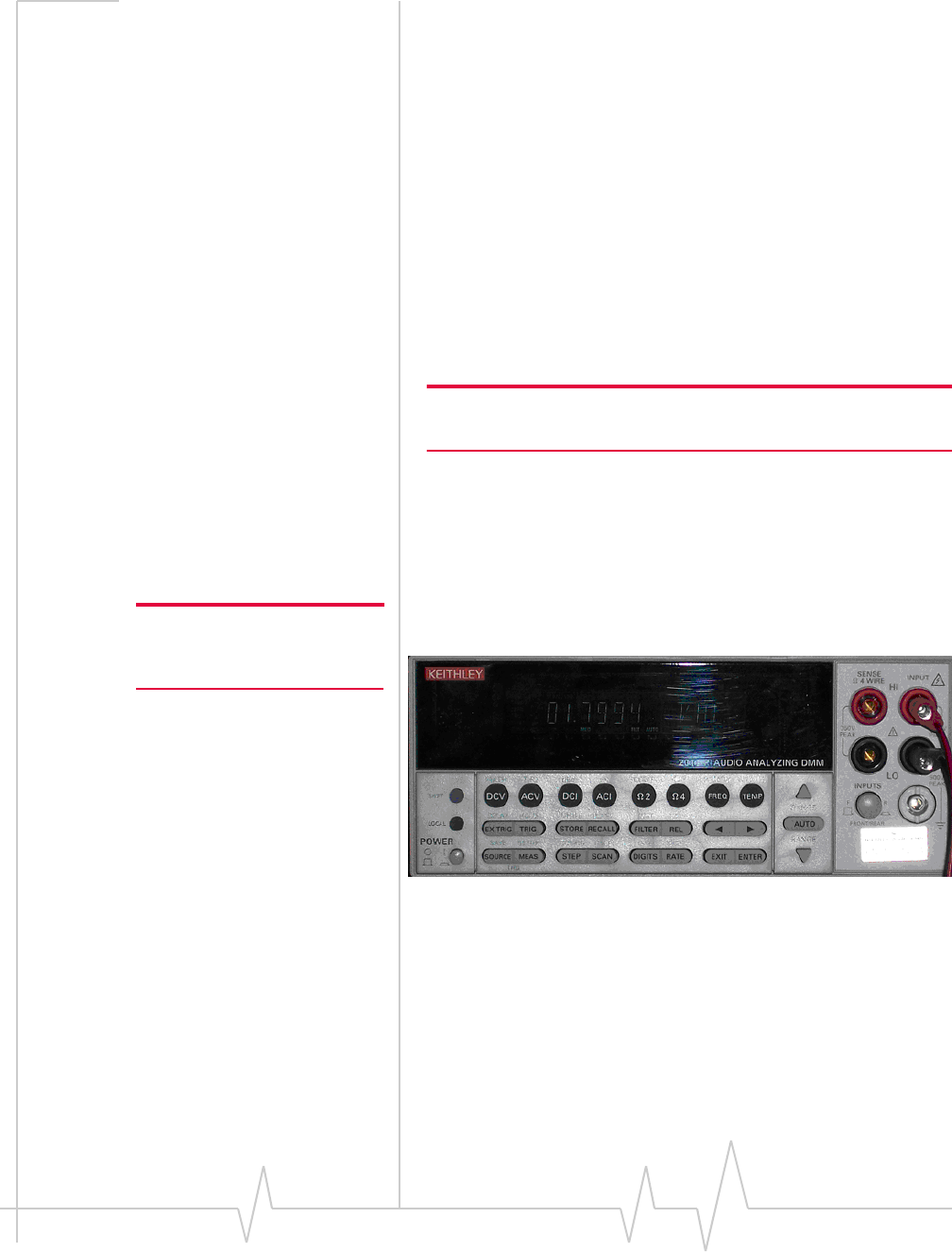
CDMA and GSM / UMTS Mini Card Hardware Integration Guide
94 Proprietary and Confidential 2130114
In the event of a discrepancy in values between this guide and the Product Specification Document (PSD), the PSD takes precedence.
RuntenormoregoodDUTsthroughthistestproce‐
duretoobtainaveragedC/Nreadings.
·TheGPSreceiverrespondstosignallevelsfrom
‐130dBmto‐80dBm.
·MeasureC/NfivetimesforeachDUTtoobtainan
averagereadingat‐110dB.
·MakesuretheC/Nislessthan15dBwhenthesignal
generatorisoff.
·Allowfor±5dBofC/Nvariationtoidentifyany
problemsintheGPSreceivepath.
Test Audio Loop-back—MC5725V /
MC5727V / MC5728V / MC8775V /
MC8785V / MC8790V / MC8791V /
MC8792V
Note: This procedure segment is performed in Step 16 of the
Suggested test plan procedure (page 84).
Themicrophoneandspeakeraudiopathsforvoice‐enable
modulescanbetestedbyusinganaudioquantitythatissuited
toidentifyknownassemblyissues,andapplyinglimitsto
detectanyproblems.
Totesttheaudiopaths:
Note: This procedure describes
steps using the Keithley Audio
Analyzing DMM, 2016-P.
1. Setuptheaudioanalyzertogenerateaconstanttone:
a. ConnectaBNCcabletothe“SourceOutput”portat
therearpanel.
b. PresstheSourcebuttononthefrontpaneltosetthe
generatorto:
·Ampl=0.20V
·Impedance=50Ω
·Freq=1.000kHz
c. IfusingaSierraWirelessMiniCardDevKit,connect
thesignalsasfollows:
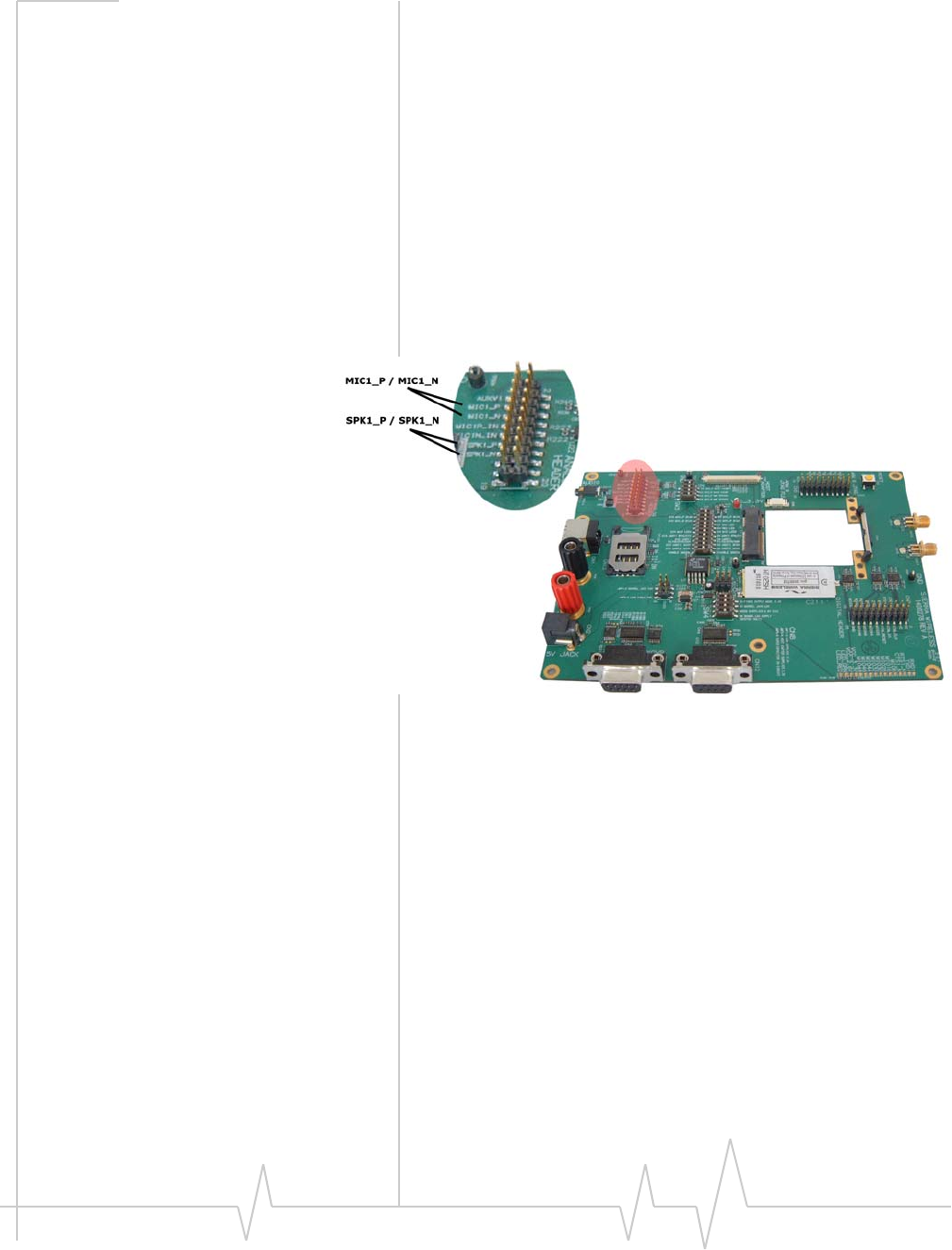
Testing
Rev 1.9.1 Feb.09 Proprietary and Confidential 95
In the event of a discrepancy in values between this guide and the Product Specification Document (PSD), the PSD takes precedence.
i. ConnectthegeneratoroutputsignaltotheMIC1_P
(positive)andMIC1_N(negative)headerpins
locatedatCN18ontheDevKit.
ii. ConnecttheanalyzerinputsignaltotheSPK1_P
(positive)andSPK1_N(negative)headerpinslocated
atCN18ontheDevKit(seeFigure8‐1).For
additionaldetailsconcerninguseoftheDevKit,see
thePCIExpressMiniCardDevKitQuickStartGuide
(Document2130705).
d. Ifusingacustomhostplatform:
i. Connectthegeneratoroutputtothemicrophone
input(MIC,positiveandnegative)inthehost.
ii. ConnecttheanalyzerinputtotheSpeakeroutput
(SPK,positiveandnegative)inthehost.
Figure 8-1: Mini Card Dev Kit showing MIC / SPK pins.
2. SetuptheDUTusingthefollowingcommands:
(MC5725V/MC5727V/MC5728V)
a. AT!OEM=176 (UnlockstheextendedATcommand
set)
b. AT!DIAG (SetsmodeminDiagnosticmode)
c. AT!AVAUDIOLPBK=1 (Enablesaudioloop‐backmode)
d. AT!CODECGAIN=8000,8000,8000(Setscodecgainsin
theloopbackpathto+6dB(Tx),+6dB(Rx)and‐6dB
(SideTone).)
·Totalloopbackgain=Σ(codecgains)‐2dB
·Forthisexample,totalloopbackgain=+4dB
(MC8775V/MC8785V/MC8790V/MC8791V/MC8792V)
a. AT!UNLOCK=”<lockCode>” (UnlocksextendedAT
commandset)
b. AT!AVSETDEV=0,0,0 (Unmutesspeakerand
microphoneforaudioprofile0)

CDMA and GSM / UMTS Mini Card Hardware Integration Guide
96 Proprietary and Confidential 2130114
In the event of a discrepancy in values between this guide and the Product Specification Document (PSD), the PSD takes precedence.
c. AT!AVCODECSTG=0,FFFF (Setssidetonegainfor
audioprofile0)
3. Takemeasurementsusingthefollowingcommands(Note
thatthemodulehasagainof4dBinaudioloopback
mode.)
Note: Actual measured results
will vary, depending on your
testing setup.
a. PresstheACVbuttontomeasuretheAClevel.
·Expectedrange:1–2.5VAC
b. PresstheFREQbuttontomeasurethefrequency.
·Expectedvalue:1kHz
c. PresstheShiftandTHDbuttonsatthesametimeto
measurethetotalharmonicdistortion.
·Expectedvalue:<1%
d. Resettheaudioparameters:
·(MC5725V/MC5727V/MC5728V)
AT!AVAUDIOLPBK=0 (Disablesaudioloop‐back
mode)
·(MC8775V/MC8785V/MC8790V/MC8791V/
MC8792V)
AT!AVDEF (Setsconfigurableaudio
parameterstodefaultvalues)
Quality assurance testing
Note: QA is an ongoing process
based on random samples from
a finished batch of devices.
Thequalityassuranceteststhatyouperformonyourfinished
productsshouldbedesignedtoverifytheperformanceand
qualityofyourdevices.
Thefollowingaresometestingsuggestionsthatcanconfirm
thattheantennaisinterfacedproperly,andtheRFmoduleis
calibratedandperformstospecifications:
•Moduleregistrationoncellularnetworks
•Powerconsumption
•Originateandterminatedataandvoice(ifapplicable)calls
•Cellhand‐off
•Transmitterandreceivertests
•FER(FrameErrorRate)asanindicatorofreceiversensi‐
tivity/performance
•Channelandaveragepowermeasurementstoverifythat
thedeviceistransmittingwithinproductspecifications
•RFsensitivitytests
•MC57xx‐specific:
·Waveformqualitytests(calculatingthe“rho”parameter)
tocomparetheCDMAsignal’spowerdistribution
againsttheidealdistribution—rhomustbe>0.97with
maxfreqerrorof0.5topass.
·FERtesting—testthereceiversensitivityforconditions
ofminimumcellpower.FERcanbemeasuredforthe

Testing
Rev 1.9.1 Feb.09 Proprietary and Confidential 97
In the event of a discrepancy in values between this guide and the Product Specification Document (PSD), the PSD takes precedence.
specifiedreceiversensitivityof‐104dBm.Theobjective
ofthistestistodetermineiftheFERmeasurediswithin
theacceptablelimitsforthespecifiedreceiversensitivity
ofthemodule.UnliketheFERtestsperformedduring
productiontesting,thistestdeterminesthereceiver
performancewithouttheinfluenceofthenoisefactor
(AWGN),butwithextremelylowcellpower.The
reportedFERandtheconfidencelevelmustbe<1%and
>95%respectivelyforthetesttobeconsideredapass.
•MC87xx‐specific:
·RFsensitivitytesting:BER/BLERfordifferentbands
andmodes
·Transmitterandreceivertests(basedonrelevantsections
ofthe3GPPTS51010and3GPP34121documents)
Suggested testing equipment
Toperformproductionandpost‐productiontests,yourequire
appropriatetestingequipment.
Figure8‐2showsasuggestedteststationforusewithdevices
incorporatingeithertheMC57xxortheMC87xx.
Intheteststationasshown,atestcomputercoordinates
testingbetweenthehostdevicewithanintegratedmoduleand
themeasurementequipment.Ifthetestcomputerdoesnot
havedirectaccesstothemodule,thenthehostdevicemust
havecustomsoftwaretoforwardinstructionsfromthetest
computertothemodule.
Thissuggestedstationsetupincludes:
•Audioanalyzer—toevaluateTx
•Powermeter—toevaluatecurrentconsumptionforTxand
Rxinvariousmodes
•Signalgenerator—toevaluateRx
Whenusingthissetup,youcanallowthesignalgeneratorto
runcontinuouslythroughouttheproductiontesting
procedure.

CDMA and GSM / UMTS Mini Card Hardware Integration Guide
98 Proprietary and Confidential 2130114
In the event of a discrepancy in values between this guide and the Product Specification Document (PSD), the PSD takes precedence.
Figure 8-2: Recommended production test setup
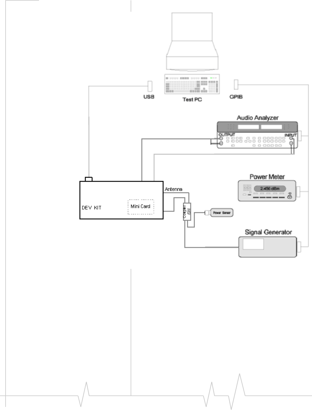

CDMA and GSM / UMTS Mini Card Hardware Integration Guide
100 Proprietary and Confidential 2130114
In the event of a discrepancy in values between this guide and the Product Specification Document (PSD), the PSD takes precedence.
A
Rev 1.9.1 Feb.09 Proprietary and Confidential 101
In the event of a discrepancy in values between this guide and the Product Specification Document (PSD), the PSD takes precedence.
A: Antenna Specification
Thisappendixdescribeselectricalperformancecriteriafor
mainpath,diversitypath,andGPSantennasusedwith
MC57xxmodules(CDMAnetworks)andMC87xxmodules
(GSM/EDGE/UMTSnetworks).
Required antennas
TableA‐1listsminimumrequiredantennatypesforeach
moduleandthemaximumantennagain,includingcableloss,
inamobile‐onlyexposurecondition.
Note: If your system uses both the MC87xx and MC57xx, the five-
band antenna can be used for both modules. However, improved
antenna performance may be attained if a dual-band main-path
antenna is designed and optimized specifically for the MC57xx.
Table A-1: Required antennas and maximum antenna gain by module type
Antenna type (minimum) Maximum antenna gaina
Module Main Diversity / GPS Cellular band
(dBi) PCS band
(dBi)
MC5725
2-band (Cellular / PCS) 3-band (Cellular / PCS / GPS)
5.1 4.15
MC5725V 5.1 4.15
MC5727 5.1 4.15
MC5727V 5.1 4.15
MC5728 TBD TBD
MC5728V TBD TBD
MC8775 N.America: 2-band
(Cellular/PCS)
Eur/Asia: 3-band
World: 5-band
n/a
5 4
MC8775V N.America: 2-band
(Cellular/PCS)
Eur/Asia: 3-band
World: 5-band
1-band (GPS) 5 4
MC8780 Eur/Asia: 3-band 3-band (Cellular / IMT / GPS) 5 4
CDMA and GSM / UMTS Mini Card Hardware Integration Guide
102 Proprietary and Confidential 2130114
In the event of a discrepancy in values between this guide and the Product Specification Document (PSD), the PSD takes precedence.
Frequency bands
TableA‐2andTableA‐3summarizethefrequencybandsthat
mustbesupportedbymain,diversity,andGPSantennasfor
CDMAandUMTSmodules.
MC8781 N.America: 2-band
(Cellular / PCS) 3-band (Cellular / PCS / GPS) 5 4
MC8785V
MC8790
MC8790V
MC8791V
MC8792V
N.America: 2-band
(Cellular/PCS)
Eur/Asia: 3-band
World: 5-band
N.America: 3-band (Cell / PCS / GPS)
Eur/Asia: 3-band (Cell / IMT / GPS)
World: 4-band (Cell / IMT / PCS / GPS)
5 4
a. Gain limits in this table are as reported on FCC grants for each module, for consideration against RF exposure and ERP / EIRP limits.
Table A-1: Required antennas and maximum antenna gain by module type
Antenna type (minimum) Maximum antenna gaina
Module Main Diversity / GPS Cellular band
(dBi) PCS band
(dBi)
Table A-2: Supported frequency bands (CDMA modules)
Module Band Antenna Mode Frequency
range
MC57xx Cell Main /
Diversity (Rx) Tx 824–849
Rx 869–894
PCS Main /
Diversity (Rx) Tx 1850–1910
Rx 1930–1990
GPS Diversity or separate
GPS antenna Rx 1574–1576
Table A-3: Supported frequency bands (UMTS modules)
Main antenna Diversity / GPS antenna
Module 850 900 1800 1900 2100 GPS 850 900 1900 2100
MC8775 YYYYY
MC8775V Y Y Y Y Y Ya
MC8780 Y Y Y Y Y YbY Y
MC8781 Y Y Y Y Y YbY Y
MC8785V Y Y Y Y Y YbY Y Y
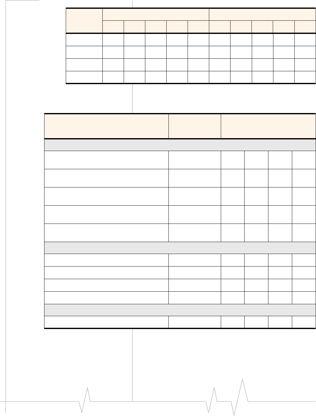
Antenna Specification
Rev 1.9.1 Feb.09 Proprietary and Confidential 103
In the event of a discrepancy in values between this guide and the Product Specification Document (PSD), the PSD takes precedence.
MC8790 Y Y Y Y Y YbY Y Y
MC8790V Y Y Y Y Y YbY Y Y
MC8791V Y Y Y Y Y YbY
MC8792V Y Y Y Y Y YbY Y Y
a. GPS supported on separate GPS antenna
b. GPS supported on diversity antenna
Table A-4: Supported frequency bands (main / diversity / GPS antennas)
Frequency band Frequency
range (MHz) Supported network types
GSM GPRS EDGE UMTS
Main Antenna
850 (North America) Tx: 824–849
Rx: 869–894 Y Y Y Y
900 (Europe) Tx: 880–915
Rx: 925–960 Y Y Y
1800 (Europe) Tx: 1710–1785
Rx: 1805–1880 Y Y Y
1900 (North America) Tx: 1850–1910
Rx: 1930–1990 Y Y Y Y
2100 (Europe) Tx: 1920–1980
Rx: 2110–2170 Y
Diversity / GPS Antenna (if GPS is enabled)
UMTS850 (North America) Rx: 869-894 Y
UMTS1900 (PCS North America) Rx: 1930–1990 Y
UMTS2100 (IMT Europe) Rx: 2110–2170 Y
GPS (Worldwide) Rx: 1574–1576
Secondary (GPS) Antenna
GPS (Worldwide) Rx: 1574–1576
Table A-3: Supported frequency bands (UMTS modules)
Main antenna Diversity / GPS antenna
Module 850 900 1800 1900 2100 GPS 850 900 1900 2100

CDMA and GSM / UMTS Mini Card Hardware Integration Guide
104 Proprietary and Confidential 2130114
In the event of a discrepancy in values between this guide and the Product Specification Document (PSD), the PSD takes precedence.
Antenna design
Designofmainpath,diversitypath,andGPSantennasis
determinedbythehostdeviceOEMandtheirdesignated
antennadesigner.
Note: Modems that support diversity and GPS can use the same
secondary (diversity) antenna for both.
Note: Antennas should be designed BEFORE the industrial design is
finished to make sure that the best antennas can be developed.
General antenna design requirements
InadditiontopassingthespecifictestsdescribedinTesting
beginningonpage106,themainpathanddiversity/GPSpath
antennasshouldsatisfythefollowingrequirements:
•Antennaimpedanceatfeedingterminal=50Ω(Asimple
matchingcircuitwithsixorfewercomponentsisacceptable
atthefeedingterminal.)
•Nominallyomni‐directionalradiationpatterninthe
azimuthplane
Main antenna design requirements
InadditiontopassingthespecifictestsdescribedinTesting
beginningonpage106,themainpathantennashouldsatisfy
thefollowingrequirements:
•Musthandle2WRFpoweronlowbandsand1Wonhigh
bands
Measurethepowerusingthefollowingcriteria:
•Measurepowerenduranceoveraperiodof4hours
(estimatedtalktime)usinga2WCWsignal—setthe
frequencyoftheCWtestsignaltothemiddleofthePCSTx
band(1880MHzforPCS).
•Visualinspectionmustprovethereisnodamagetothe
antennastructureandmatchingcomponents.
•VSWR/TIS/TRPmeasurementstakenbeforeandafterthis
testmustshowsimilarresults.

Antenna Specification
Rev 1.9.1 Feb.09 Proprietary and Confidential 105
In the event of a discrepancy in values between this guide and the Product Specification Document (PSD), the PSD takes precedence.
Diversity antenna design requirements
(MC57xx / MC8780 / MC8781 / MC8785V /
MC8790 / MC8790V / MC8791V /
MC8792V)
Antennadiversityisrequiredforenduserperformanceand
enhancedcoverageonCDMAnetworks(800MHz/
1900MHz)forMC57xx,andonUMTSnetworks(850MHz/
1900MHz/2100MHz)forMC8780/MC8781/MC8785V/
MC8790/MC8790V/MC8791V/MC8792V.(SeeTableA‐3on
page102forUMTSdiversitysupportbymodule.)
InadditiontopassingthespecifictestsdescribedinTesting
beginningonpage106,thediversitypathantennashould
satisfythefollowingrequirement:
•Receiveperformance,measuredbyforwardlink
throughput,mustbe0to3dBbetterthanasingleantenna
Performance goals
Whendesigningtheantennasystem,considerthefollowing
performancegoals:
•0dBgainantenna(orbetter)
•Diversityantennareceiveperformancetobesimilarto
primaryantenna
•Separationdistanceorpolarityseparationtoachieve
diversityantennaisolationof10db(minimum)—otherwise
thereceiveantennapicksuptoomuchpowerradiating
fromtheprimaryantenna
GPS antenna design requirements
(MC57xx / MC8775V / MC878x)
AsecondantennaisrequiredtoaccessGPSfunctionality—if
themodemalsosupportsdiversity,thesameantennacanbe
used.
InadditiontopassingthespecifictestsdescribedinTesting
beginningonpage106,thediversitypathantennashould
satisfythefollowingrequirements:
•Fieldofview(FOV):Omni‐directionalinazimuth,‐45°to
+90°inelevation
•Polarization(averageGv/Gh):>0dB.Verticallinearpolar‐
izationissufficient(noneedtooptimizeforcircularpolar‐
ization)
•Freespaceaveragegain(Gv+Gh)overFOV:>‐6dBi
(preferably>‐3dBi).Note:Averagegainisthesumof
averagevalues(Gv+Gh)wherebothGvandGhare

CDMA and GSM / UMTS Mini Card Hardware Integration Guide
106 Proprietary and Confidential 2130114
In the event of a discrepancy in values between this guide and the Product Specification Document (PSD), the PSD takes precedence.
measured(andaveraged)over‐45°to+90°inelevationand
±180°inazimuth.
•Maximumgainanduniformcoverageinthehighelevation
angleandzenith.Gainintheazimuthplaneisnotdesired.
•Average3Dgain:>‐5dBi
•TypicalVSWR:<2:1
•Polarization:anyotherthanLHCP(left‐handcircular
polarized)isacceptable
ThesamedesignproceduresoutlinedinInterferenceand
sensitivityonpage41applytotheGPSpathaswell.
Testing
Theperformancespecificationsdescribedinthissectionare
validwhiletheantennaismountedinthehostdevicewiththe
antennafeedcableroutedinitsfinalapplicationconfiguration.
Thefollowingguidelinesapplytothetestsinthissection:
•Performelectricalmeasurementsatroomtemperature
(+20°Cto+26°C)unlessotherwisespecified
•Formainanddiversitypathantennas,makesurethe
antennas(includingcontactdevice,coaxialcable,
connectors,andmatchingcircuitwithnomorethansix
components,ifrequired)havenominalimpedancesof50Ω
acrossthefrequencybandsinTableA‐4.
•Alltests(exceptisolation/correlationcoefficient)—testthe
mainordiversityantennawiththeotherantennatermi‐
nated.
•Anymetallicpartoftheantennasystemthatisexposedto
theoutsideenvironmentneedstomeettheelectrostatic
dischargetestsperIEC61000‐4‐2(conducteddischarge
+8kV).
•Thefunctionalrequirementsoftheantennasystemare
testedandverifiedwhiletheMiniCardantennais
integratedinthehostdevice.
Note: Additional testing, including active performance tests,
mechanical, and accelerated life tests can be discussed with Sierra
Wireless’ engineering services. Contact your Sierra Wireless repre-
sentative for assistance.
Voltage Standing Wave Ratio (VSWR)
MeasureVSWRforeachantenna(main,diversity)usingthe
followingcriteria:
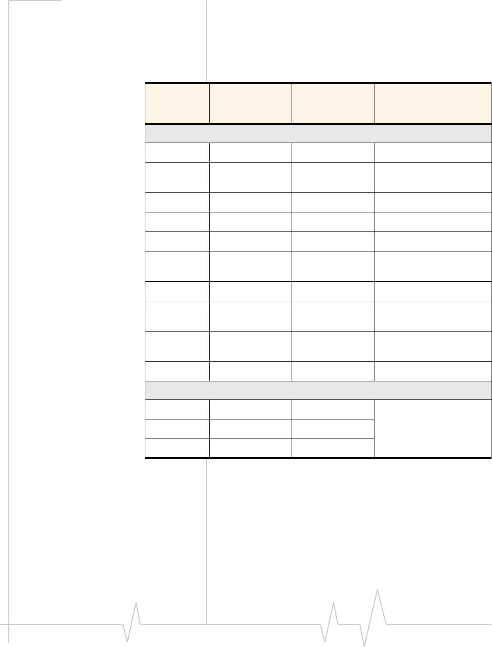
Antenna Specification
Rev 1.9.1 Feb.09 Proprietary and Confidential 107
In the event of a discrepancy in values between this guide and the Product Specification Document (PSD), the PSD takes precedence.
•MeasureVSWRinfreespaceattheantenna’scoaxial
connector(feedingterminal)whentheantennaisinstalled
inthehostdevicewiththecableroutedtotheMiniCard
slot.
•UseanHP8753Enetworkanalyzer(orequivalent).
Table A-5: VSWR (Voltage Standing Wave Ratio)
Frequency
(MHz) Typical VSWR Worst-case
VSWR at band
edges
Notes
Main antenna
824–849 2.5:1 850-band Tx
869–880 3.5:1 850-band Rx excluding
part inside 900-band Tx
880–915 2.5:1 900-band Tx
925–960 3.5:1 900-band Rx
1710–1785 2.5:1 1800-band Tx
1805–1850 3.5:1 1800-band Rx excluding
part inside 1900-band Tx
1850–1910 2.5:1 1900-band Tx
1920–1980 2.5:1 2100-band Tx and part of
1900-band Rx
1980–1990 3.5:1 Part of 1900-band Rx
outside of 2100-band Tx
2110–2170 3.5:1 2100-band Rx
Diversity / GPS antenna
869–894 < 3:1 <3.5:1
Preferable to have input
VSWR < 2:1
1930–1990 < 3:1 <3.5:1
2110–2170 < 3:1 <3.5:1
CDMA and GSM / UMTS Mini Card Hardware Integration Guide
108 Proprietary and Confidential 2130114
In the event of a discrepancy in values between this guide and the Product Specification Document (PSD), the PSD takes precedence.
Efficiency
TableA‐6detailstheminimumtotalradiatedefficiencyfor
mainand,ifsupported,diversityantennas.
Antenna-to-antenna isolation
(MC57xx/MC8775V/MC878x)
Useanetworkanalyzertomeasureisolationbetweenthemain
andsecondaryantennapairsovertheoperatingTx/Rx
frequencybandsdescribedinTableA‐4onpage103.
TableA‐7detailstheminimumisolationallowedoverthe
variousfrequencybandsfortheapplicableantennapairs.
Whenyouperformthesetests:
•Iftheantennascanbemoved,testallpositionsforboththe
mainandsecondaryantennas.
•Collectworst‐caseisolationdata.
•Makesureallotherwirelessdevices(BluetoothorWLAN
antennas,etc.)areturnedOFFtoavoidinterference.For
details,seeInterferencefromotherwirelessdeviceson
page41.
Note: System performance below the minimum isolation specification
could cause damage to the module, resulting in below-average
system performance.
Table A-6: Minimum total radiated efficiencya
a. Total efficiency is measured at the RF connec-
tor. It includes mismatch losses, losses in the
matching circuit, and antenna losses.
Mode Main Diversity
Transmit (Tx) 50% n/a
Receive (Rx) 30% 25%
Table A-7: Minimum Main–Secondary antenna isolation
Antenna pair
Isolation (dB)
850 / 900 band GPS band DCS / PCS /
UMTS band
Main / Diversity (Tx and Rx) 8 (cell) 8 (PCS / UMTS)
Main (Tx) / GPS 15 15 15
Antenna Specification
Rev 1.9.1 Feb.09 Proprietary and Confidential 109
In the event of a discrepancy in values between this guide and the Product Specification Document (PSD), the PSD takes precedence.
Peak gain and radiation patterns
TableA‐8describesthepeakandaverageantennagainlimits
forthemainpathanddiversitypathantennas.
Note: Sierra Wireless recommends using antenna efficiency as the
primary parameter for evaluating the antenna system.
Antenna Peak Gain is not a good indication of antenna performance
when integrated with a host device; the antenna does NOT provide
omni-directional gain patterns. Peak Gain performance can be
affected by parameters such as antenna size, location, design type,
etc. The antenna gain patterns remain fixed unless one or more of
these parameters changes.
Table A-8: Peak and average antenna gain
Antenna Peak gaina
a. Vertical / horizontal polarizations
Main > +1 dBi > -3 dBi
Diversity > -3 dBi > -6 dBi
Fading correlation coefficient
(MC57xx/MC878x)
Measurethefading(envelope)correlationcoefficientbetween
themainanddiversityantennasovertheoperatingRx
frequencybandsdescribedinTableA‐4.
Themaximumallowedfadingcorrelationcoefficientoverany
ofthebandsis0.5.
Average gainb
b. Vertical / horizontal polarizations combined, over ±45° in eleva-
tion and ±180° in azimuth

CDMA and GSM / UMTS Mini Card Hardware Integration Guide
110 Proprietary and Confidential 2130114
In the event of a discrepancy in values between this guide and the Product Specification Document (PSD), the PSD takes precedence.

B
Rev 1.9.1 Feb.09 Proprietary and Confidential 111
In the event of a discrepancy in values between this guide and the Product Specification Document (PSD), the PSD takes precedence.
B: Regulatory Information
Important notice
Becauseofthenatureofwirelesscommunications,trans‐
missionandreceptionofdatacanneverbeguaranteed.Data
maybedelayed,corrupted(i.e.,haveerrors)orbetotallylost.
Althoughsignificantdelaysorlossesofdataarerarewhen
wirelessdevicessuchastheSierraWirelessmodemareusedin
anormalmannerwithawell‐constructednetwork,theSierra
Wirelessmodemshouldnotbeusedinsituationswherefailure
totransmitorreceivedatacouldresultindamageofanykind
totheuseroranyotherparty,includingbutnotlimitedto
personalinjury,death,orlossofproperty.SierraWirelessand
itsaffiliatesacceptnoresponsibilityfordamagesofanykind
resultingfromdelaysorerrorsindatatransmittedorreceived
usingtheSierraWirelessmodem,orforfailureoftheSierra
Wirelessmodemtotransmitorreceivesuchdata.
Safety and hazards
DonotoperateyourMC57xx/MC87xxmodem:
•Inareaswhereblastingisinprogress
•Whereexplosiveatmospheresmaybepresentincluding
refuellingpoints,fueldepots,andchemicalplants
•Nearmedicalequipment,lifesupportequipment,orany
equipmentwhichmaybesusceptibletoanyformofradio
interference.Insuchareas,theMC57xx/MC87xxmodem
MUSTBEPOWEREDOFF.Otherwise,theMC57xx/
MC87xxmodemcantransmitsignalsthatcouldinterfere
withthisequipment.
Inanaircraft,theMC57xx/MC87xxmodemMUSTBE
POWEREDOFF.Otherwise,theMC57xx/MC87xxmodem
cantransmitsignalsthatcouldinterferewithvariousonboard
systemsandmaybedangeroustotheoperationoftheaircraft
ordisruptthecellularnetwork.Useofacellularphoneinan
aircraftisillegalinsomejurisdictions.Failuretoobservethis
instructionmayleadtosuspensionordenialofcellular
telephoneservicestotheoffender,orlegalactionorboth.
Someairlinesmaypermittheuseofcellularphoneswhilethe
aircraftisonthegroundandthedoorisopen.TheMC57xx/
MC87xxmodemmaybeusednormallyatthistime.

CDMA and GSM / UMTS Mini Card Hardware Integration Guide
112 Proprietary and Confidential 2130114
In the event of a discrepancy in values between this guide and the Product Specification Document (PSD), the PSD takes precedence.
Important compliance
information for North American
users
TheMC57xx/MC87xxmodemhasbeengrantedmodular
approvalformobileapplications.Integratorsmayusethe
MC57xx/MC87xxmodemintheirfinalproductswithout
additionalFCC/IC(IndustryCanada)certificationifthey
meetthefollowingconditions.Otherwise,additionalFCC/IC
approvalsmustbeobtained.
1. Atleast20cmseparationdistancebetweentheantenna
andtheuser’sbodymustbemaintainedatalltimes.
2. TocomplywithFCC/ICregulationslimitingboth
maximumRFoutputpowerandhumanexposuretoRF
radiation,themaximumantennagainincludingcableloss
inamobile‐onlyexposureconditionmustnotexceedthe
levelsdetailedinTableA‐1,“Requiredantennasand
maximumantennagainbymoduletype,”onpage101.
3. TheMC57xx/MC87xxmodemanditsantennamustnot
beco‐locatedoroperatinginconjunctionwithanyother
transmitterorantennawithinahostdevice.
4. Alabelmustbeaffixedtotheoutsideoftheendproduct
intowhichtheMC57xx/MC87xxmodemisincorporated,
withastatementsimilartothefollowing:
·ForMC5725/MC5725V:
ThisdevicecontainsFCCID:N7N‐MC5725
Thisequipmentcontainsequipmentcertifiedunder
IC:2417C‐MC5725
·ForMC5727/MC5727V:
ThisdevicecontainsFCCID:N7N‐MC5727
Thisequipmentcontainsequipmentcertifiedunder
IC:2417C‐MC5727
·ForMC5728/MC5728V:
ThisdevicecontainsFCCID:N7N‐MC5728
Thisequipmentcontainsequipmentcertifiedunder
IC:2417C‐MC5728
·ForMC8775/MC8775V:
ThisdevicecontainsFCCID:N7NMC8775
Thisequipmentcontainsequipmentcertifiedunder
IC:2417C‐MC8775
·ForMC8780:
ThisdevicecontainsFCCID:N7NMC8780
·ForMC8781:
ThisdevicecontainsFCCID:N7NMC8781
Thisequipmentcontainsequipmentcertifiedunder
IC:2417C‐MC8781

Regulatory Information
Rev 1.9.1 Feb.09 Proprietary and Confidential 113
In the event of a discrepancy in values between this guide and the Product Specification Document (PSD), the PSD takes precedence.
·ForMC8785V:
ThisdevicecontainsFCCID:N7NMC8785
Thisequipmentcontainsequipmentcertifiedunder
IC:2417C‐MC8785
·ForMC8790/MC8790V:
ThisdevicecontainsFCCID:N7NMC8790
Thisequipmentcontainsequipmentcertifiedunder
IC:2417C‐MC8790
·ForMC8792V:
ThisdevicecontainsFCCID:N7NMC8792
Thisequipmentcontainsequipmentcertifiedunder
IC:2417C‐MC8792
5. Ausermanualwiththeendproductmustclearlyindicate
theoperatingrequirementsandconditionsthatmustbe
observedtoensurecompliancewithcurrentFCC/ICRF
exposureguidelines.
TheendproductwithanembeddedMC57xx/MC87xx
modemmayalsoneedtopasstheFCCPart15unintentional
emissiontestingrequirementsandbeproperlyauthorizedper
FCCPart15.
Note:Ifthismoduleisintendedforuseinaportabledevice,
youareresponsibleforseparateapprovaltosatisfytheSAR
requirementsofFCCPart2.1093andICRSS‐102.
EU regulatory conformity
SierraWirelessherebydeclaresthattheMC8775,MC8775V,
MC8780,MC8781,MC8785V,MC8790,MC8790V,MC8791V,
andMC8792Vmodemsconformwithallessentialrequire‐
mentsofDirective1999/5/EC.
TheDeclarationofConformitymadeunderDirective1999/5/
ECisavailableforviewingatthefollowinglocationintheEU
community:
SierraWireless(UK),Limited
LakesideHouse
1FurzegroundWay,StockleyParkEast
Uxbridge,Middlesex
UB111BD
England

CDMA and GSM / UMTS Mini Card Hardware Integration Guide
114 Proprietary and Confidential 2130114
In the event of a discrepancy in values between this guide and the Product Specification Document (PSD), the PSD takes precedence.
C
Rev 1.9.1 Feb.09 Proprietary and Confidential 115
In the event of a discrepancy in values between this guide and the Product Specification Document (PSD), the PSD takes precedence.
C: Acronyms and Definitions
.
Table C-9: Acronyms and definitions
Acronym or term Definition
AGC Automatic Gain Control
BER Bit Error Rate - a measure of receive sensitivity
BLER Block Error Rate
Call Box Base Station Simulator - Agilent E8285A or 8960, Rohde &
Schwarz CMU200
CDMA Code Division Multiple Access
dB Decibel = 10 x log10 (P1/P2)
P1 is calculated power; P2 is reference power
Decibel = 20 x log10 (V1/V2)
V1 is calculated voltage, V2 is reference voltage
dBm Decibels, relative to 1 mW - Decibel(mW) = 10 x log10 (Pwr (mW)/
1mW)
DUT Device Under Test
EDGE Enhanced Data rates for GSM Evolution
EM Embedded Module
ESD ElectroStatic Discharge
FER Frame Error Rate - a measure of receive sensitivity
GPRS General Packet Radio Services
GPS Global Positioning System
GSM Global System for Mobile communications
Hz Hertz = 1 cycle/second
inrush current Peak current drawn when a device is connected or powered on
IS-2000 3G radio standards for voice and data (CDMA only)
IS-95 2G radio standards targeted for voice (cdmaONE)
LDO Low Drop Out - refers to linear regulator
CDMA and GSM / UMTS Mini Card Hardware Integration Guide
116 Proprietary and Confidential 2130114
In the event of a discrepancy in values between this guide and the Product Specification Document (PSD), the PSD takes precedence.
MC5725 / MC5725V /
MC5727 / MC5727V /
MC5728 / MC5728V
Sierra Wireless Mini Cards used on CDMA networks
MC57xx Any of the following CDMA Mini Cards: MC5725 / MC5725V /
MC5727 / MC5727V / MC5728 / MC5728V
MC8775 / MC8775V /
MC8780 / MC8781 /
MC8785V / MC8790 /
MC8790V / MC8791V /
MC8792V
Sierra Wireless Mini Cards used on GSM / UMTS networks
MC87xx Any of the following GSM / UMTS Mini Cards: MC8775 / MC8775V /
MC8780 / MC8781 / MC8785V / MC8790 / MC8790V / MC8791V /
MC8792V
MHz MegaHertz = 10E6 Hertz (Hertz = 1 cycle/second)
MIO Module Input/Output
MPE Maximum Permissible Exposure — the level of radiation to which a
person may be exposed without hazardous effect or adverse
biological changes
OTA Over-The-Air or Radiated through the antenna
PCS Personal Communication System - PCS spans the 1.9 GHz radio
spectrum
RF Radio Frequency
RMS Root Mean Square
SA Selective Availability
Sensitivity (Audio) Measure of lowest power signal that the receiver can measure
Sensitivity (RF) Measure of lowest power signal at the receiver input that can
provide a prescribed BER / BLER / SNR value at the receiver
output.
SIM Subscriber Identity Module
SNR Signal to Noise Ratio
SOF Start of Frame - a USB function
UART Universal Asynchronous Receiver Transmitter
UDK Universal Development Kit (PCI Express Mini Card Dev Kit)
UMTS Universal Mobile Telecommunications System
Table C-9: Acronyms and definitions
Acronym or term Definition

Acronyms and Definitions
Rev 1.9.1 Feb.09 Proprietary and Confidential 117
In the event of a discrepancy in values between this guide and the Product Specification Document (PSD), the PSD takes precedence.
USB Universal Serial Bus
USIM Universal Subscriber Identity Module
VCC3.3 3.3 V supply voltage
WCDMA Wideband Code Division Multiple Access — In this document, the
term “UMTS” is used instead of “WCDMA”.
XIM In this document, XIM is used as part of the contact identifiers for
the USIM interface (XIM_VCC, XIM_CLK, etc.).
Table C-9: Acronyms and definitions
Acronym or term Definition

CDMA and GSM / UMTS Mini Card Hardware Integration Guide
118 Proprietary and Confidential 2130114
In the event of a discrepancy in values between this guide and the Product Specification Document (PSD), the PSD takes precedence.

Rev 1.9.1 Feb.09 Proprietary and Confidential 119
In the event of a discrepancy in values between this guide and the Product Specification Document (PSD), the PSD takes precedence.
Index
Numerics
1X
CDMAStandard13
A
acceptancetests77
acronymsanddefinitions115–117
airplanemode19
anechoicchamber,OTAtesting43
antenna
connectionandmountingpoints39
connectionconsiderations39
custom,considerations40
designrequirements,diversityantenna105
designrequirements,general104
designrequirements,GPS105
designrequirements,mainantenna104
diversityantenna,disabling41
diversity,MC57xx105
frequencybands,supported102
GPS,MC8775V/MC8780/MC8781105
limit,matchingcoaxialconnections39
location,considerations40
matching,considerations40
maximumcableloss39
specification101–109
testing106
antennas
designchecklist75
frequencybandssupported,byantennatype
103
frequencybandssupported,MC57xx102
frequencybandssupported,MC87xx102
required,bymoduletypeandgain101
ATcommands
3GPPspecification,details13
extended,MC57xx68
extended,MC87xx69
extended,overview68
lowpowermode,setting20
standard,MC57xx(referencedocument)13
standard,MC87xx(referencedocument)15
ATcommands,extended
MC57xx,reference13
MC87xx,reference15
ATcommands,standard
MC57xx,reference13
MC87xx,reference15
audio
features,summary51
functions,host‐controlled58
functions,module‐controlled58
functions,responsiblecodecs52
interface51–59
pathmixing,host‐controlled59
pathswitching,host‐controlled58
PCMdigital,signalinterface58
primary,signalinterface57
signalinterface57
systemblockdiagram,MC5725V52
systemblockdiagram,MC5727V52
systemblockdiagram,MC8775V54
audiomodes,supported55
audiopassband51
audiopassband,RxandTx57
automaticgaincontrol(AGC)
module‐controlled58
B
BER(BitErrorRate)45
biterrorrate(BER)
measureofsensitivity,MC87xx45
C
cableloss
antenna,maximum39
capacitance
inrushcurrent,effecton25
capacitors
withUSIM68
withXIM_DATA/XIM_CLK67
carkitaudiomode51
carkitmode
echocancellation56
CDMA
1XStandard13
cellularband
RFparameters,MC57xx37
certificationtests78
checklist,design75
CnS
MC57xxreference13
MC87xxreference15
notificationissued,statechange
temperature23
voltage21
codec
foraudiofunctions52
comfortnoise
module‐controlled58
communications,hosttomodem
designchecklist76
connection
grounding39
connectors,required

CDMA and GSM / UMTS Mini Card Hardware Integration Guide
120 Proprietary and Confidential 2130114
In the event of a discrepancy in values between this guide and the Product Specification Document (PSD), the PSD takes precedence.
EDGEmating(52‐pin)12
host‐module12
RF,Hirose12
USIM12
current
consumption27–35
usagemodels35
peakinrushcurrent,calculation25
specifications,MC57xx28
specifications,MC8775/75V28–30
specifications,MC8780/8130–31
specifications,MC8785V31–32,32–33
current,consumption27
D
DCS1800
RFparameters,MC87xx37
sensitivity,testresults48
desense.SeeRF
designchecklist
antennas75
componentplacement75
EMI/ESD76
host/modemcommunications76
power75
thermal76
device
positioning,sensitivitytesting45
disconnected,modulepowerstate19
diversityantenna
disabling41
DTMF
codec52
module‐controlled58
E
echocancellation
audiofeature51
codec52
details56
module‐controlled58
support,allmodes56
EDGEconnector,manufacturers12
efficiency
testcriteria108
EGSM900
RFparameters,MC87xx37
sensitivity,testresults47
electrostaticdischarge.SeeESD
ESD
designchecklist76
protectionrequirements18
testingtechniquesdocument(IEC‐61000‐4‐2)14
F
fadingcorrelationcoefficient
testcriteria109
FCC
regulations,relevantsection13
FER(FrameErrorRate)45
filtering
highpass/slopefiltering,module‐controlled58
filteringstages,audio51
filtering,RFdesense43
FIRfiltering
audiofeature51
codec52
module‐controlled58
frameerrorrate(FER)
measureofsensitivity,MC57xx45
frequencybands,supported102
G
gain
codec52
distribution,audio56
limits,adjustable51
gain,antenna
testcriteria109
GPSband
RFparameters,MC57xx37
RFparameters,MC87xx38
GPSsensitivity
conducted,RFparameter,MC87xx37
grounding
connectionconsiderations39
GSM1900
sensitivity,testresults48
GSM850
RFparameters,MC87xx37
sensitivity,testresults47
H
handsetaudiomode51
handsetmode
echocancellation56
handshaking
USB62
headsetaudiomode51
headsetmode
echocancellation56
Host⁄Moduleinterface61–71
I
I/Orisetimerequirements67
impedance
module‐antenna41
USIM67

Index
Rev 1.9.1 Feb.09 Proprietary and Confidential 121
In the event of a discrepancy in values between this guide and the Product Specification Document (PSD), the PSD takes precedence.
inrushcurrents
description24
hostpowersupplyapplied25
model,MC57xx24
model,MC87xx25
W_Disable#deasserted25
interface
audiosignal57
interference
devicegenerated42
powersupplynoise41
wirelessdevices41
isolation
testcriteria108
L
LED
example65
states64
lowpowermode
setting,ATcommands20
statechangefromnormal,temperature23
statechangefromnormal,voltage21
statechangetonormal,temperature23
statechangetonormal,voltage21
temperaturetriggerlevels22
voltagetriggerlevels20
lowpower,modulepowerstate19–20
M
MC5725
ATcommands,extended68
ATreference(extended)13
ATreference(standard)13
CnSreference13
networkssupported11
productspecification14
RFparameters(MC57xx)37
MC5725V
ATcommands,extended68
audiointerface,supported51
productspecification14
RFparameters(MC57xx)37
MC5727
ATreference(extended)13
ATreference(standard)13
CnSreference13
RFparameters(MC57xx)37
MC5727V
ATcommands,extended68
audiointerface,supported51
RFparameters(MC57xx)37
MC57xx
currentspecifications28
sensitivitytestresults46
sensitivity,defined45
MC8755
CnSreference,andMC87xx15
MC8755V
CnSreference,andMC87xx15
MC8765
CnSreference,andMC87xx15
MC8775
ATcommands,extended,andMC87xx69
ATreference(extended),andMC87xx15
ATreference(standard),andMC87xx15
CnSreference,andMC87xx15
currentspecifications28–30
networkssupported11
productspecification14
RFparameters37
MC8775V
ATcommands,extended,andMC87xx69
ATreference(extended),andMC87xx15
ATreference(standard),andMC87xx15
audiointerface,supported51
CnSreference,andMC87xx15
currentspecifications28–30
networkssupported11
pins,connector(2.6V)61
productspecification14,15
RFparameters37
MC8780
ATcommands,extended,andMC87xx69
ATreference(extended),andMC87xx15
ATreference(standard),andMC87xx15
currentspecifications30–31
networkssupported11
powerconsumption34
productspecification14
RFparameters37
MC8781
ATcommands,extended,andMC87xx69
ATreference(extended),andMC87xx15
ATreference(standard),andMC87xx15
currentspecifications30–31
networkssupported11
powerconsumption34
productspecification14
RFparameters37
MC8785V
currentspecifications31–32,32–33
networkssupported11
MC87xx
sensitivitytestresults47–50
sensitivity,defined45
MiniCard
DevKitQuickStartGuide15
PCIExpressSpecification15
SeealsoMC5725,MC5725V,MC5727,MC5727V,
MC8775,MC8775V,MC8780,MC8781,
MC8785V
minicom
downloadingandinstalling84
mixing

CDMA and GSM / UMTS Mini Card Hardware Integration Guide
122 Proprietary and Confidential 2130114
In the event of a discrepancy in values between this guide and the Product Specification Document (PSD), the PSD takes precedence.
codec52
modes
deepsleep,description34
operating34
shutdown,description34
sleep,description34
transmit/receive,description34
module
powerstates18–24
N
networks
supported,bymoduletype11
noise
leakage,minimizing39
RFinterference,powersupply41
noisesuppression
audiofeature51
module‐controlled58
normalmode
statechangefromlowpower,temperature23
statechangefromlowpower,voltage21
statechangetolowpower,temperature23
statechangetolowpower,voltage21
normal,modulepowerstate19
O
off,modulepowerstate19
outputdriverstage,audiofeature51
P
pathloss,OTAtesting44
pathswitching
codec52
PCB
multi‐layer,shieldingforRFdesense43
PCIExpress
MiniCardspecification15
PCMdigitalaudio,signalinterface58
PCS1900
RFparameters,MC87xx37
PCSband
RFparameters,MC57xx37
pins
connector(2.6V),MC8775V61
polyphonicringtone
host‐controlled58
power
consumption,MC8780/8134
currentconsumption,overview27
defaultstate19
designchecklist75
disconnected,characteristics19
normal,characteristics19
off,characteristics19
off,statechange,temperature23
off,statechange,voltage21
power‐uptiming26
ramp‐uptiming26
requiredsupplyvoltage17
signals,overview17
statemachine,temperaturemonitoring22–24
statemachine,voltagemonitoring20–22
state,disconnected19
state,lowpower19–20
state,normal19
state,off19
states,module18–24
supply,RFinterference41
supply,ripplelimit41
transmit,waveform26
powerinterface17–35
productspecification(PSD)14
productiontests79
PSD(ProductSpecificationDocument)14
Q
qualityassurancetests96
R
regulatoryinformation111–113
EU113
FCC112
limitationofliability111
safetyandhazards111
resistors,externalpull‐up67
resume
mode,USB63
RF
antennacableloss,maximum39
antennaconnection,considerations39
cabletype,required12
desense
device‐generated42
harmonicenergy,filtering43
mitigationsuggestions42
shieldingsuggestions43
integration37–50
interference
otherdevices42
powersupply41
wirelessdevices41
levelloweredautomatically,hightemperature24
parameters
cellularband,MC57xx37
GPS,MC57xx37
MC57xx37
MC87xx37
PCSband,MC57xx37
parameters,MC87xx
DCS180037

Index
Rev 1.9.1 Feb.09 Proprietary and Confidential 123
In the event of a discrepancy in values between this guide and the Product Specification Document (PSD), the PSD takes precedence.
EGSM90037
GPS38
GSM85037
PCS190037
UMTS190038
UMTS210038
UMTS85038
ringertone
codec52
ringers
module‐controlled58
ringtone,polyphonic
host‐controlled58
Rxband
RFparameters,MC57xx37
Rxsensitivity
conducted,RFparameter,MC87xx37
RFparameter,MC57xx37
S
SCI(SlotCycleIndex)28
SED
seeSmartErrorDetection
sensitivity
conducted,RFparameter,MC87xx37
defined,MC57xxandMC87xx45
GPSconducted,MC87xx37
MC57xx,defined(frameerrorrate)45
MC87xx,defined(biterrorrate)45
measurements47–50
radiatedmeasurement,overview43
RFparameter,MC57xx37
testresults
MC57xx46
MC87xx47–50
testing
deviceundertest,positioning45
testing,overview43
testing,pathlosscalculation44
sensitivity,OTAtestchamberconfiguration43
shielding
module,compliance40
reducingRFdesense43
sidetone
responsiblecodec59
support55
SIM
testingmethods,MSconformancespecification15
SeealsoUSIM
SlotCycleIndex28
SmartErrorDetection
detectingmodulereset34
speakerphoneaudiomode51
speakerphonemode
echocancellation57
statemachine
temperaturemonitoring22–24
voltagemonitoring20–22
suspend
mode,USB63
systemblock
MC5725V,audio52
MC5727V,audio52
MC8775V,audio54
T
temperaturemonitoringstatemachine
triggerlevels22
temperature,module.Seethermal
test
efficiency108
fadingcorrelationcoefficient109
gain,antenna109
isolation108
VSWR(VoltageStandingWaveRatio)106
testing
overview77
acceptancetests77
audioloop‐back,MC5725V/MC5727V/MC8775V
94
certificationtests78
equipment,suggested97
ESDimmunity,techniquesdocument(IEC‐61000‐
4‐2)14
GPSreceiver,MC8775V/MC8780/MC878193
manualfunctionaltest,suggested80
productiontests79
qualityassurancetests96
RFreceivepath,MC57xx88
RFreceivepath,MC87xx90
RFtransmissionpath,MC57xx85
RFtransmissionpath,MC87xx86
sensitivity,OTAtestchamberconfiguration43
suggestions77–99
testing,pathlosscalculation45
thermal
considerations73–74
designchecklist76
dissipation,factorsaffecting73
dissipation,suggestions73
RFshieldtemperature,maximum74
testing,module73–74
timing
powerramp‐up26
power‐up26
transducerinterface
host‐controlled59
transducerinterfaces
codec52
transmitpowerwaveform26
Txband
RFparameters,MC57xx37
Txpower
conducted,RFparameter,MC87xx37
RFparameters,MC57xx37

CDMA and GSM / UMTS Mini Card Hardware Integration Guide
124 Proprietary and Confidential 2130114
In the event of a discrepancy in values between this guide and the Product Specification Document (PSD), the PSD takes precedence.
U
UDK(UniversalDevelopmentKit)
components,included11
UMTS1900
RFparameters,MC87xx38
sensitivity,testresults50
UMTS2100
RFparameters,MC87xx38
sensitivity,testresults50
UMTS850
RFparameters,MC87xx38
sensitivity,testresults49
UniversalDevelopmentKit(UDK)
components,included11
UniversalSerialBus.SeeUSB.
usagemodels
currentconsumption35
USB
enumeration,power‐up26
handshaking62
hostdriverrequirements63
interface
host⁄modulecommunication62–64
overview62
resumemode63
specification15
suspendmode63
USIM
capacitorrecommendations68
cardcontacts66
clockrate67
connectortype,required12
electricalspecifications67
impedance,connectors67
interfacediagram66
interface,overview65
operation67–68
pinassignments65
socketplacement68
V
voicememo
host‐controlled58
voltagemonitoringstatemachine
triggerlevels20
VoltageStandingWaveRatio(VSWR)
testcriteria106
volume,setting
responsiblecodec59
VSWR(VoltageStandingWaveRatio)
testcriteria106
W
W_Disable#
deasserted,causesinrushcurrentevent25
de‐asserted,peakcurrent25
inrushcurrents24
module,poweringoff21,23
Normalstate19
offstate19
Z
ZIF(ZeroIntermediateFrequency)41
