Sierra Wireless P5186-SK GSM/GPRS Starter Kit P5186 User Manual WM PRJ WM3 3 PTS 005 001
Sierra Wireless, Inc. GSM/GPRS Starter Kit P5186 WM PRJ WM3 3 PTS 005 001
UserManual.wiki
>
Sierra Wireless
>
P5186 SK User Manual
Users Manual
Navigation menu
Upload a User Manual
Namespaces
Wiki Guide
HTML
PDF
Info
Views
User Manual
Discussion / Help
Navigation
![ERROR! REFERENCE SOURCE NOT FOUND.P5186 USER MANUAL V 1.0 Error! Reference source not found. Reference documents [1] MOTHER BOARD Starter kit Schematics and PCB, Release 2.0 Ref.: WM01048-010-20. [2] WISMO Pac P5186 module Product Technical Specification Ref.: WM_PRJ_P5100_PTS_001. [3] Firmware downloader User Guide Ref.: WM_SW_GEN_UGD_001. confidential © Page : 7 / 42This document is the sole and exclusive property of WAVECOM. Not to be distributed or divulged without prior written agreement. Ce document est la propriété exclusive de WAVECOM. Il ne peut être communiqué ou divulgué à des tiers sans son autorisation préalable.](https://usermanual.wiki/Sierra-Wireless/P5186-SK/User-Guide-368454-Page-7.png)
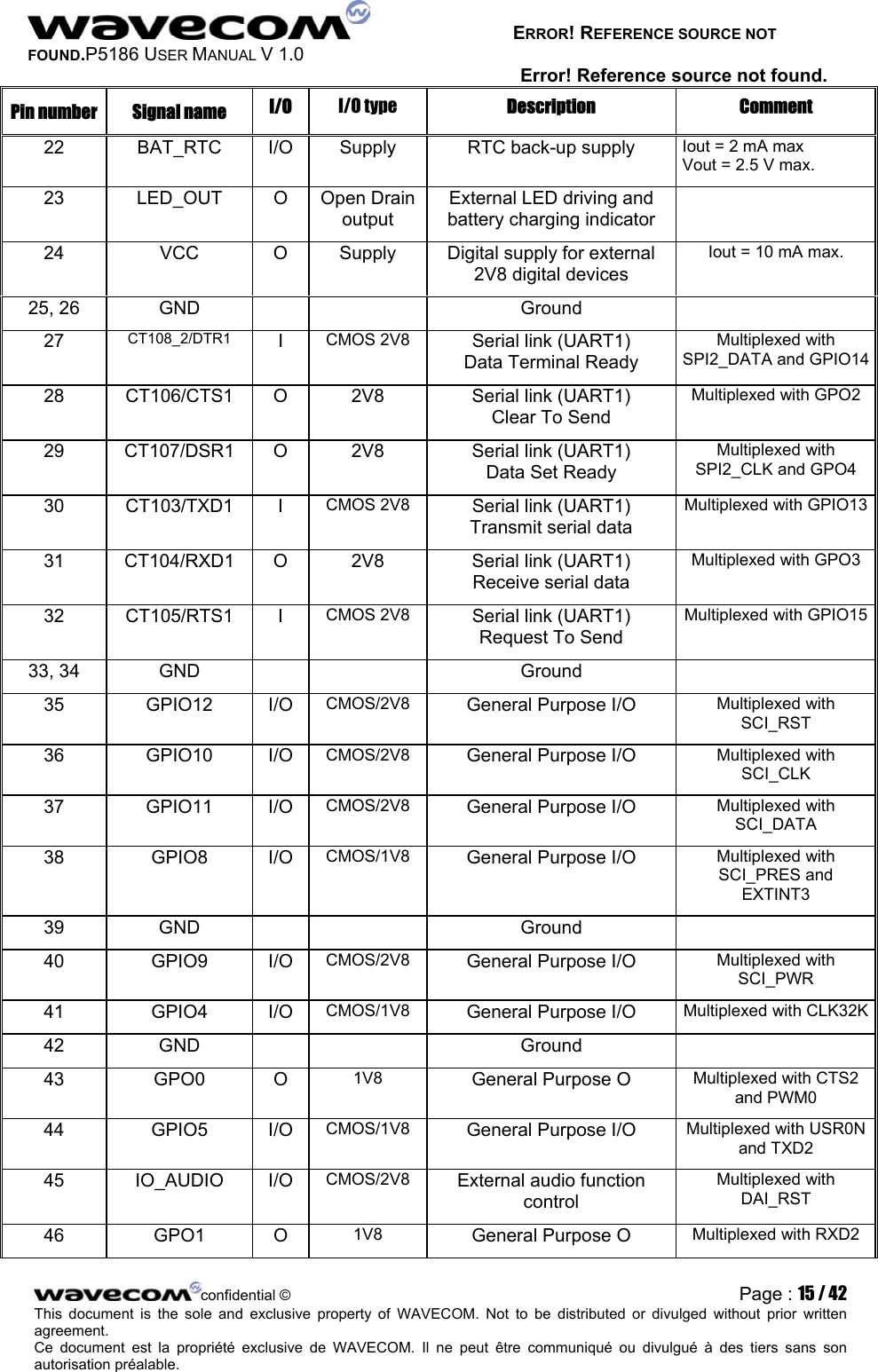
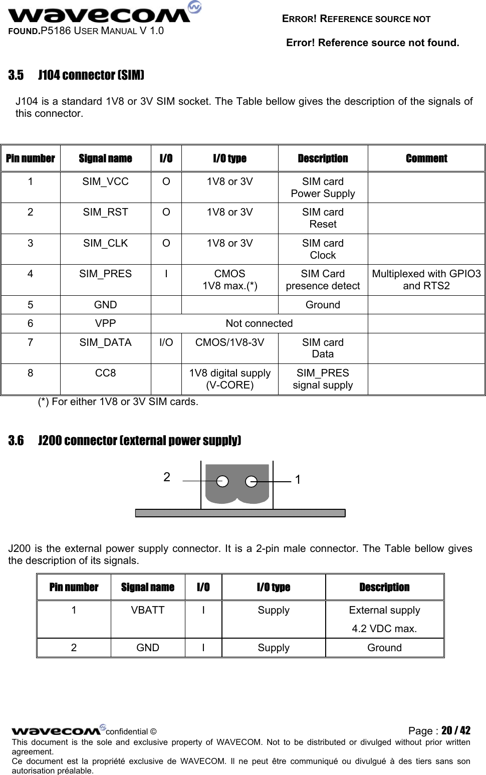
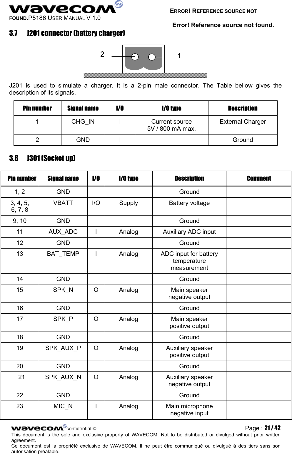
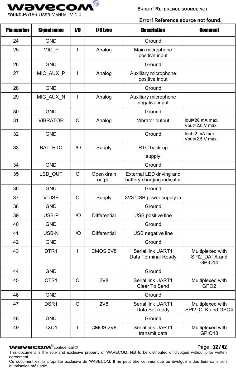
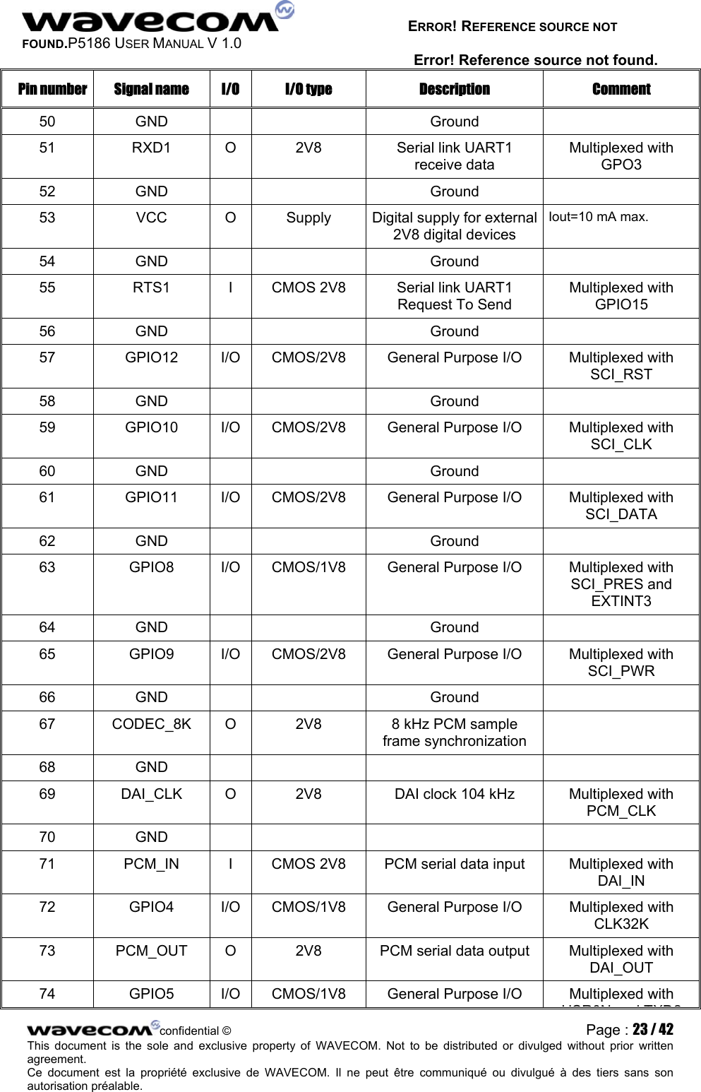
![ERROR! REFERENCE SOURCE NOT FOUND.P5186 USER MANUAL V 1.0 Error! Reference source not found. 3 Connector description 3.1 WISMO Pac P5186 signals Some of the WISMO Pac P5186 interface signals mentioned hereafter are multiplexed in order to limit the number of pins. For further information about the WISMO Pac P5186 signals and multiplexing, refer to document [2] WISMO Pac P5186 module Product Technical Specification Ref.: WM_PRJ_P5100_PTS_001. 3.2 J100 connector J100 is a HE10 50-pin male connector. Pin number Signal name I/O I/O type Description Comment 1, 2 GND Ground 3, 4 VBATT I/O Battery voltage High current. 5, 6 GND Ground . 7 AUX_ADC I Analog Auxiliary ADC input 8 BAT_TEMP I Analog ADC input for battery temperature measurement 9, 10 GND Ground . 11 SPK_N O Analog Main speaker negative output 12 SPK_P O Analog Main speaker positive output 13 SPK_AUX_P O Analog Auxiliary speaker positive output 14 SPK_AUX_N O Analog Auxiliary speaker negative output 15 MIC_N I Analog Main microphone negative input 16 MIC_P I Analog Main microphone positive input 17 MIC_AUX_P I Analog Auxiliary microphone positive input 18 MIC_AUX_N I Analog Auxiliary microphone negative input 19, 20 GND Ground 21 VIBRATOR O Analog Vibrator output Iout = 80 mA max Vout = 2.8 V max. confidential © Page : 14 / 42This document is the sole and exclusive property of WAVECOM. Not to be distributed or divulged without prior written agreement. Ce document est la propriété exclusive de WAVECOM. Il ne peut être communiqué ou divulgué à des tiers sans son autorisation préalable.](https://usermanual.wiki/Sierra-Wireless/P5186-SK/User-Guide-368454-Page-14.png)
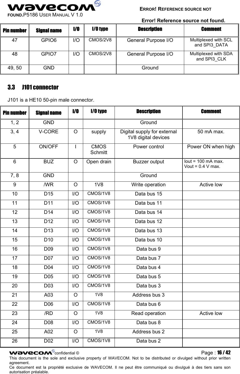
![ERROR! REFERENCE SOURCE NOT FOUND.P5186 USER MANUAL V 1.0 Error! Reference source not found. Pin number Signal name I/O I/O type Description Comment 36 Not Connected 37, 38, 39 GND Ground 40 /RESET I/O Schmitt Module RESET 41 DAI_CLK O 2V8 DAI clock 104 kHz Multiplexed with PCM_CLK 42 PCM_OUT O 2V8 PCM serial data Output Multiplexed with DAI_OUT 43 CODEC_8K O 2V8 8 kHz PCM sample frame synchronization 44 PCM_IN I CMOS 2V8 PCM serial data Input Multiplexed with DAI_IN45 TP1 Test Point TP1* 46 TP2 Test Point TP2* 47, 48, 49, 50 GND Ground * refer to document [1] for further details. confidential © Page : 19 / 42This document is the sole and exclusive property of WAVECOM. Not to be distributed or divulged without prior written agreement. Ce document est la propriété exclusive de WAVECOM. Il ne peut être communiqué ou divulgué à des tiers sans son autorisation préalable.](https://usermanual.wiki/Sierra-Wireless/P5186-SK/User-Guide-368454-Page-19.png)
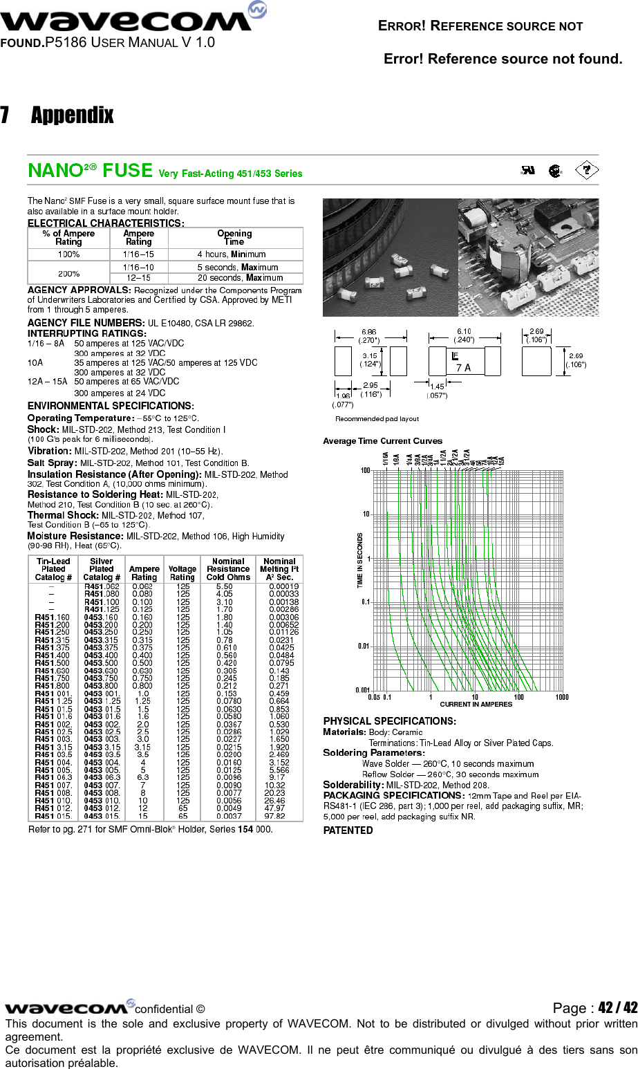
![ERROR! REFERENCE SOURCE NOT FOUND.P5186 USER MANUAL V 1.0 Error! Reference source not found. 6.2 Trouble shooting If I=0 on the external power supply amperemeter, then: o Check that the external power supply: Is “ON”. is connected on J200. is adjusted for an output voltage between 3.2 V and 4.2 V. o Check that the “ON/OFF” switch (SW201) is “ON”. o Check the fuse F1 (3 A) and replace it if necessary. Note: technical characteristics of the fuse to be replaced are given in appendix. o Check the configuration of the jumpers on switch SW200. If the WISMO module does not reply to the “AT↵” command (no message “OK” is received), make sure that: o The WISMO module is present on the mother board (socket up mounted). o a software has been loaded in the module (refer to the documentation [3]). 6.3 Safety, FCC and Industry of Canada Regulatory compliance 6.3.1 RF safety 6.3.1.1 General Your GSM terminal1 is based on the GSM standard for cellular technology. The GSM standard is spread all over the world. It covers Europe, Asia and some parts of America and Africa. This is the most used telecommunication standard. Your GSM terminal is actually a low power radio transmitter and receiver. It sends out and receives radio frequency energy. When you use your GSM application, the cellular system which handles your calls controls both the radio frequency and the power level of your cellular modem. 6.3.1.2 Exposure to RF energy There has been some public concern about possible health effects of using GSM terminals. Although research on health effects from RF energy has focused on the current RF technology for many years, scientists have begun research regarding newer radio technologies, such as GSM. After existing research had been reviewed, and after compliance to all applicable safety standards had been tested, it has been concluded that the product was fitted for use. If you are concerned about exposure to RF energy there are things you can do to minimize exposure. Obviously, limiting the duration of your calls will reduce your exposure to RF energy. In addition, you can reduce RF exposure by operating your cellular terminal efficiently by following the below guidelines. confidential © Page : 38 / 42This document is the sole and exclusive property of WAVECOM. Not to be distributed or divulged without prior written agreement. Ce document est la propriété exclusive de WAVECOM. Il ne peut être communiqué ou divulgué à des tiers sans son autorisation préalable. 1 based on WISMO2D](https://usermanual.wiki/Sierra-Wireless/P5186-SK/User-Guide-368454-Page-38.png)