Sierra Wireless P5186-SK GSM/GPRS Starter Kit P5186 User Manual WM PRJ WM3 3 PTS 005 001
Sierra Wireless, Inc. GSM/GPRS Starter Kit P5186 WM PRJ WM3 3 PTS 005 001
Users Manual

WISMO Pac P5100 series
WISMO Pac P5186 module
Starter kit User Guide
Reference: P5186-SK User Manual
Version: 1.1
Date: September 30, 2003
confidential © Page : 1 / 42
This document is the sole and exclusive property of WAVECOM. Not to be distributed or divulged without prior written
agreement.
Ce document est la propriété exlcusive de WAVECOM. Il ne peut être communiqué ou divulgué à des tiers sans son
autorisation préalable.
ERROR! REFERENCE SOURCE NOT
FOUND.P5186 USER MANUAL V 1.0
Error! Reference source not found.
Document Information
Revision Date History of the evolution
001 28 May 2003 Creation
1.1 23 oct. 03
confidential © Page : 2 / 42
This document is the sole and exclusive property of WAVECOM. Not to be distributed or divulged without prior written
agreement.
Ce document est la propriété exclusive de WAVECOM. Il ne peut être communiqué ou divulgué à des tiers sans son
autorisation préalable.

ERROR! REFERENCE SOURCE NOT
FOUND.P5186 USER MANUAL V 1.0
Error! Reference source not found.
Contents
Document Information ...........................................................................................................................................................................................2
Contents........................................................................................................................................................................................................................ 3
Cautions ........................................................................................................................................................................................................................ 5
Trademarks ................................................................................................................................................................................................................. 5
Overview........................................................................................................................................................................................................................ 6
Reference documents ............................................................................................................................................................................................ 7
List of abbreviations ............................................................................................................................................................................................... 8
1 Mother board block diagram............................................................................................................................................................... 9
2 Hardware description ........................................................................................................................................................................... 10
2.1 Mother board .......................................................................................................................... 10
2.2 Socket up................................................................................................................................ 12
2.3 Antenna connection................................................................................................................ 13
3 Connector description...........................................................................................................................................................................14
3.1 WISMO Pac P5186 signals .................................................................................................... 14
3.2 J100 connector ....................................................................................................................... 14
3.3 J101 connector ....................................................................................................................... 16
3.4 J102 connector ....................................................................................................................... 18
3.5 J104 connector (SIM) ............................................................................................................. 20
3.6 J200 connector (external power supply) ................................................................................ 20
3.7 J201 connector (battery charger) ........................................................................................... 21
3.8 J300 (RF connector).................................................................Error! Bookmark not defined.
3.9 J301 (Socket up) .................................................................................................................... 21
3.10 J302 (Socket up)..................................................................................................................... 24
3.11 J500 connector (Auxiliary audio) ............................................................................................ 27
3.12 J501 connector (Main audio) .................................................................................................. 28
3.13 J600 connector (RS232)......................................................................................................... 29
3.14 J700 connector (USB) ............................................................................................................30
confidential © Page : 3 / 42
This document is the sole and exclusive property of WAVECOM. Not to be distributed or divulged without prior written
agreement.
Ce document est la propriété exclusive de WAVECOM. Il ne peut être communiqué ou divulgué à des tiers sans son
autorisation préalable.

ERROR! REFERENCE SOURCE NOT
FOUND.P5186 USER MANUAL V 1.0
Error! Reference source not found.
4 Operating configuration ...................................................................................................................................................................... 31
5 Functional description..........................................................................................................................................................................33
5.1 Power supply .......................................................................................................................... 33
5.2 Charger function ..................................................................................................................... 33
5.3 SIM function............................................................................................................................ 33
5.4 RS232 function ....................................................................................................................... 34
5.4.1 Introduction 34
5.4.2 Shutdown of Max3238....................................................................................................... 35
5.5 Audio functions....................................................................................................................... 35
5.6 ON/~OFF and BOOT function................................................................................................ 35
5.7 RESET function ...................................................................................................................... 36
5.8 KEYPAD function ................................................................................................................... 36
5.9 Antenna function..................................................................................................................... 36
5.10 ESD protections...................................................................................................................... 36
6 Getting started .......................................................................................................................................................................................... 37
6.1 Procedure ............................................................................................................................... 37
6.2 Trouble shooting..................................................................................................................... 38
7 Appendix.......................................................................................................................................................................................................42
confidential © Page : 4 / 42
This document is the sole and exclusive property of WAVECOM. Not to be distributed or divulged without prior written
agreement.
Ce document est la propriété exclusive de WAVECOM. Il ne peut être communiqué ou divulgué à des tiers sans son
autorisation préalable.

ERROR! REFERENCE SOURCE NOT
FOUND.P5186 USER MANUAL V 1.0
Error! Reference source not found.
Cautions
This starter kit integers a modular transmitter. This device is to be used only for mobile and fixed
applications.
The antenna(s) used for this transmitter must be installed to provide a separation distance of at least
20 cm from all persons and must not be co-located or operating in conjunction with any other
antenna or transmitter. The antenna(s) used for this transmitter must not exceed a gain of 3 dBi for
mobile operation and 7 dBi for fixed operation.
Users and OEM integrators must be provided with antenna installation instructions and transmitter
operating conditions for satisfying RF exposure compliance. OEM must also be provided with
labelling instructions.
This device contains 900 MHz GSM functions that are not operational in U.S. territories. This filing is
only applicable for GSM 850 MHz and PCS 1900 MHz operations.
Information provided herein by Wavecom is accurate and reliable. However no responsibility is
assumed for its use.
General information about Wavecom and its range of products is available at the following internet
address: http://www.wavecom.com
Trademarks
WAVECOM, WISMO are trademarks or registered trademarks of Wavecom S.A. All other company
and/or product names mentioned may be trademarks or registered trademarks of their respective
owners.
confidential © Page : 5 / 42
This document is the sole and exclusive property of WAVECOM. Not to be distributed or divulged without prior written
agreement.
Ce document est la propriété exclusive de WAVECOM. Il ne peut être communiqué ou divulgué à des tiers sans son
autorisation préalable.

ERROR! REFERENCE SOURCE NOT
FOUND.P5186 USER MANUAL V 1.0
Error! Reference source not found.
Overview
This document is a description of the WISMO Pac P5186 Starter kit based on a mother board V2
Ref. WM01048-010-20.
This Starter kit is an equipment which can be used to start software and hardware development
based on WISMO Pac P5186 modules.
Refer to the documentation of the WISMO Pac P5186 module for further information.
confidential © Page : 6 / 42
This document is the sole and exclusive property of WAVECOM. Not to be distributed or divulged without prior written
agreement.
Ce document est la propriété exclusive de WAVECOM. Il ne peut être communiqué ou divulgué à des tiers sans son
autorisation préalable.

ERROR! REFERENCE SOURCE NOT
FOUND.P5186 USER MANUAL V 1.0
Error! Reference source not found.
Reference documents
[1] MOTHER BOARD Starter kit Schematics and PCB, Release 2.0
Ref.: WM01048-010-20.
[2] WISMO Pac P5186 module Product Technical Specification
Ref.: WM_PRJ_P5100_PTS_001.
[3] Firmware downloader User Guide
Ref.: WM_SW_GEN_UGD_001.
confidential © Page : 7 / 42
This document is the sole and exclusive property of WAVECOM. Not to be distributed or divulged without prior written
agreement.
Ce document est la propriété exclusive de WAVECOM. Il ne peut être communiqué ou divulgué à des tiers sans son
autorisation préalable.

ERROR! REFERENCE SOURCE NOT
FOUND.P5186 USER MANUAL V 1.0
Error! Reference source not found.
List of abbreviations
ADC Analog to Digital Converter
AUX AUXiliary
CLK CLocK
CTS Clear To Send
DAI Digital Audio Interface
DC Direct Current
DCD Data Carrier Detect
DCE Data Communication Equipment
DSR Data Set Ready
DTE Data Terminal Equipment
DTR Data Terminal Ready
ESD ElectroStatic Discharges
GND GrouND
GPI General Purpose Input
GPIO General Purpose Input Output
GPO General Purpose Output
I/O Input / Output
MIC MICrophone
PC Personnal Computer
PCM Pulse Code Modulation
PWM Pulse Width Modulation
RF Radio Frequency
RI Ring Indicator
RTC Real Time Clock
RTS Request To Send
RXD Receive Data
SCI Smart Card Interface
SIM Subscriber Identity Module
SPI Serial Peripheral Interface
SPK SPeaKer
TXD Transmit Data
USB Universal Serial Bus
confidential © Page : 8 / 42
This document is the sole and exclusive property of WAVECOM. Not to be distributed or divulged without prior written
agreement.
Ce document est la propriété exclusive de WAVECOM. Il ne peut être communiqué ou divulgué à des tiers sans son
autorisation préalable.
ERROR! REFERENCE SOURCE NOT
FOUND.P5186 USER MANUAL V 1.0
Error! Reference source not found.
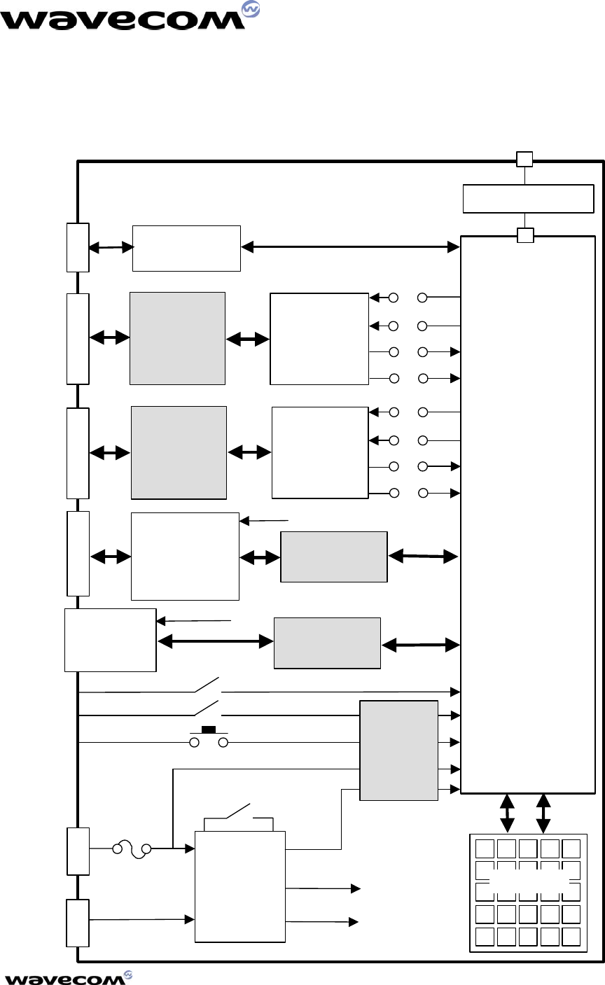
1 Mother board block diagram
Socket up
With
WISMO Pac
P5186
Module
SIM
Card
holder
RS-232
In terface
ESD
protection
ESD
protection
Pow er
Supply
J500 Auxiliary
handset
interface
JP500
JP501
JP502
JP503
J501
Main
handset
interface
JP504
JP505
JP506
JP507
J600
J104
J200
F1 (3 A )
ROW COL
Keypad
USB
In terface
M atching circuit
J
700
J201
Ex tern al
supply
Charger
inpu t
ON/~OFF
SW201
SW202 BOOT
SW203 /RESET
DVCC
DVCC
SW200
SM A300
J300
A
NT
CC8_PRES
CC8_PRES
CHG_IN
ESD
protection
ESD
protection
VBATT
ESD
protection
confidential © Page : 9 / 42
This document is the sole and exclusive property of WAVECOM. Not to be distributed or divulged without prior written
agreement.
Ce document est la propriété exclusive de WAVECOM. Il ne peut être communiqué ou divulgué à des tiers sans son
autorisation préalable.
ERROR! REFERENCE SOURCE NOT
FOUND.P5186 USER MANUAL V 1.0
Error! Reference source not found.
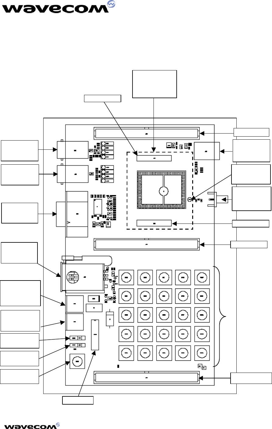
2 Hardware description
2.1 Mother board
J500
Aux. Audio
connector
J501
Main Audio
connector
J600
RS232
connector
J104
SIM
Connector
J200
Ex tern al
Supply
Conn ector
SW203
RESET J102
J101
SW400 SW405 SW410 SW415 SW420
KEYPAD
SW404 SW 409 SW414 SW419
SW200
SM A300
Antenna
Conn ector
SW202
BOOT
SW201
ON/∼OFF
J201
DC charger
In p u t
J700
USB
connector
P5186
Socket up
print
J300
Antenna
connection
J100
J301
J302
confidential © Page : 10 / 42
This document is the sole and exclusive property of WAVECOM. Not to be distributed or divulged without prior written
agreement.
Ce document est la propriété exclusive de WAVECOM. Il ne peut être communiqué ou divulgué à des tiers sans son
autorisation préalable.
ERROR! REFERENCE SOURCE NOT
FOUND.P5186 USER MANUAL V 1.0
Error! Reference source not found.
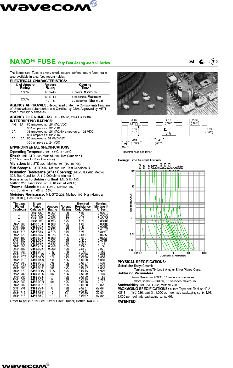
Fuse F1
(3 A )
confidential © Page : 11 / 42
This document is the sole and exclusive property of WAVECOM. Not to be distributed or divulged without prior written
agreement.
Ce document est la propriété exclusive de WAVECOM. Il ne peut être communiqué ou divulgué à des tiers sans son
autorisation préalable.
ERROR! REFERENCE SOURCE NOT
FOUND.P5186 USER MANUAL V 1.0
Error! Reference source not found.
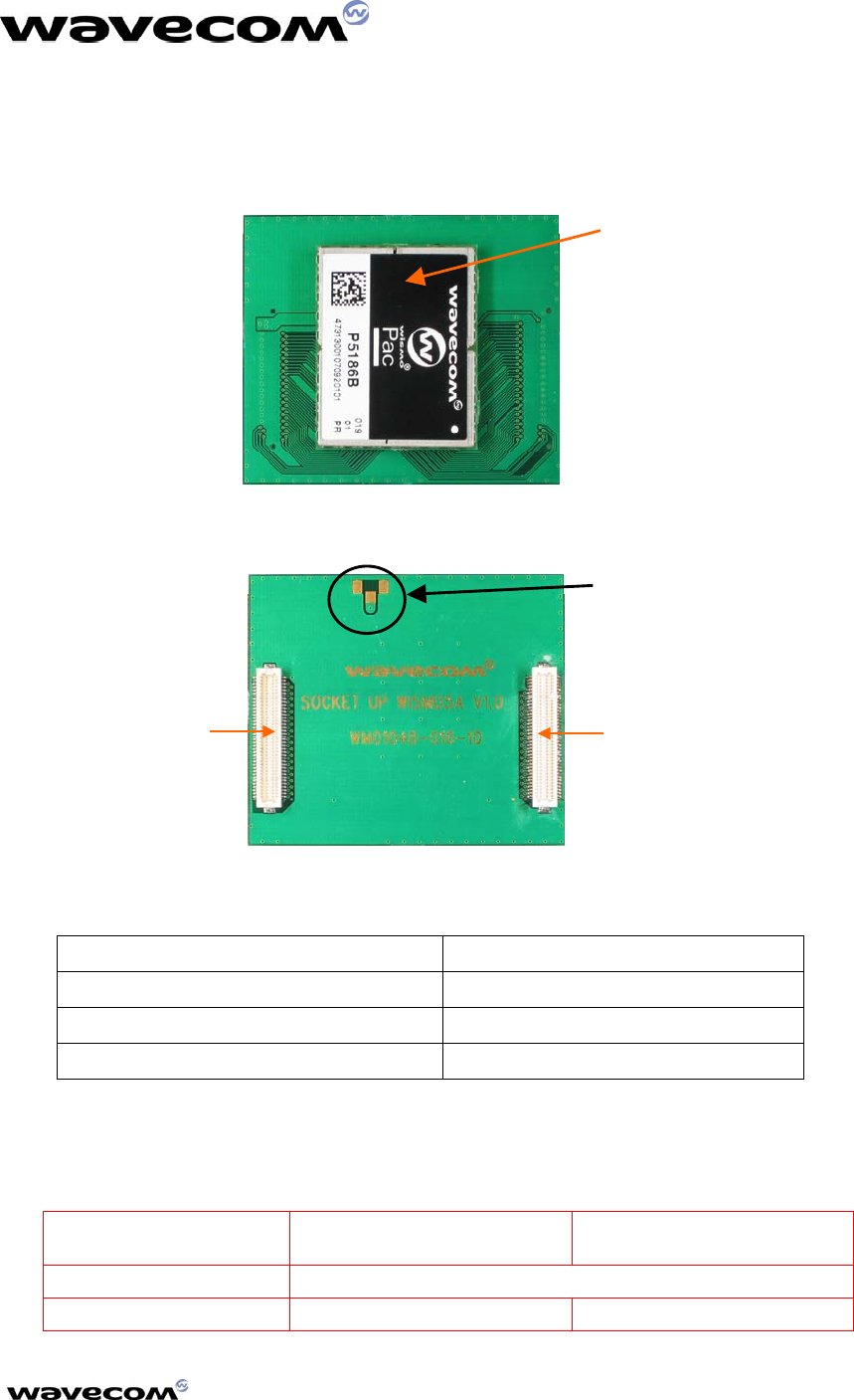
2.2 Socket up
Top view
Bottom view
WISMO
P5186
Module
J3
J2
A
ntenna
PAD
Connection to the mother board:
Socket up Mother board
Antenna PAD J300 (RF connector type IMP)
J3 J301
J2 J302
Warning:
After 50 plug in and 50 plug out of the socket up on the mother board, the efficiency of the connection
is no more guaranteed by the connector manufacturer:
Connector designation 80- pin header
on the mother board
80- pin receptacle
on the socket up
Manufacturer HIROSE
Part number DF12(3.0)-80DP-0.5V(80) DF12(3.0)-80DS-0.5V(80)
confidential © Page : 12 / 42
This document is the sole and exclusive property of WAVECOM. Not to be distributed or divulged without prior written
agreement.
Ce document est la propriété exclusive de WAVECOM. Il ne peut être communiqué ou divulgué à des tiers sans son
autorisation préalable.
ERROR! REFERENCE SOURCE NOT
FOUND.P5186 USER MANUAL V 1.0
Error! Reference source not found.
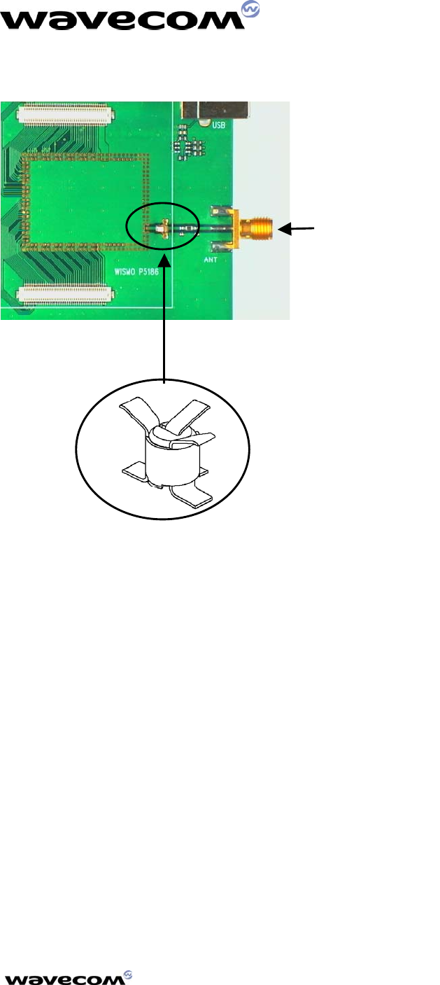
2.3 Antenna connection
SMA300
Antenna
connector
J300 (SMT connector)
Antenna connection
With the socket up
confidential © Page : 13 / 42
This document is the sole and exclusive property of WAVECOM. Not to be distributed or divulged without prior written
agreement.
Ce document est la propriété exclusive de WAVECOM. Il ne peut être communiqué ou divulgué à des tiers sans son
autorisation préalable.
ERROR! REFERENCE SOURCE NOT
FOUND.P5186 USER MANUAL V 1.0
Error! Reference source not found.
3 Connector description
3.1 WISMO Pac P5186 signals
Some of the WISMO Pac P5186 interface signals mentioned hereafter are multiplexed in order to
limit the number of pins.
For further information about the WISMO Pac P5186 signals and multiplexing, refer to document [2]
WISMO Pac P5186 module Product Technical Specification
Ref.: WM_PRJ_P5100_PTS_001.
3.2 J100 connector
J100 is a HE10 50-pin male connector.
Pin number Signal name I/O I/O type Description Comment
1, 2 GND Ground
3, 4 VBATT I/O Battery voltage High current.
5, 6 GND Ground .
7 AUX_ADC I Analog Auxiliary ADC input
8 BAT_TEMP I Analog ADC input for battery
temperature measurement
9, 10 GND Ground .
11 SPK_N O Analog Main speaker
negative output
12 SPK_P O Analog Main speaker
positive output
13 SPK_AUX_P O Analog Auxiliary speaker
positive output
14 SPK_AUX_N O Analog Auxiliary speaker
negative output
15 MIC_N I Analog Main microphone
negative input
16 MIC_P I Analog Main microphone
positive input
17 MIC_AUX_P I Analog Auxiliary microphone
positive input
18 MIC_AUX_N I Analog Auxiliary microphone
negative input
19, 20 GND Ground
21 VIBRATOR O Analog Vibrator output Iout = 80 mA max
Vout = 2.8 V max.
confidential © Page : 14 / 42
This document is the sole and exclusive property of WAVECOM. Not to be distributed or divulged without prior written
agreement.
Ce document est la propriété exclusive de WAVECOM. Il ne peut être communiqué ou divulgué à des tiers sans son
autorisation préalable.

ERROR! REFERENCE SOURCE NOT
FOUND.P5186 USER MANUAL V 1.0
Error! Reference source not found.
Pin number Signal name I/O I/O type Description Comment
22 BAT_RTC I/O Supply RTC back-up supply Iout = 2 mA max
Vout = 2.5 V max.
23 LED_OUT O Open Drain
output
External LED driving and
battery charging indicator
24 VCC O Supply Digital supply for external
2V8 digital devices
Iout = 10 mA max.
25, 26 GND Ground
27 CT108_2/DTR1 I CMOS 2V8 Serial link (UART1)
Data Terminal Ready
Multiplexed with
SPI2_DATA and GPIO14
28 CT106/CTS1 O 2V8 Serial link (UART1)
Clear To Send
Multiplexed with GPO2
29 CT107/DSR1 O 2V8 Serial link (UART1)
Data Set Ready
Multiplexed with
SPI2_CLK and GPO4
30 CT103/TXD1 I
CMOS 2V8 Serial link (UART1)
Transmit serial data
Multiplexed with GPIO13
31 CT104/RXD1 O 2V8 Serial link (UART1)
Receive serial data
Multiplexed with GPO3
32 CT105/RTS1 I
CMOS 2V8 Serial link (UART1)
Request To Send
Multiplexed with GPIO15
33, 34 GND Ground
35 GPIO12 I/O
CMOS/2V8 General Purpose I/O Multiplexed with
SCI_RST
36 GPIO10 I/O
CMOS/2V8 General Purpose I/O Multiplexed with
SCI_CLK
37 GPIO11 I/O
CMOS/2V8 General Purpose I/O Multiplexed with
SCI_DATA
38 GPIO8 I/O
CMOS/1V8 General Purpose I/O Multiplexed with
SCI_PRES and
EXTINT3
39 GND Ground
40 GPIO9 I/O
CMOS/2V8 General Purpose I/O Multiplexed with
SCI_PWR
41 GPIO4 I/O
CMOS/1V8 General Purpose I/O Multiplexed with CLK32K
42 GND Ground
43 GPO0 O
1V8 General Purpose O Multiplexed with CTS2
and PWM0
44 GPIO5 I/O
CMOS/1V8 General Purpose I/O Multiplexed with USR0N
and TXD2
45 IO_AUDIO I/O
CMOS/2V8 External audio function
control
Multiplexed with
DAI_RST
46 GPO1 O
1V8 General Purpose O Multiplexed with RXD2
confidential © Page : 15 / 42
This document is the sole and exclusive property of WAVECOM. Not to be distributed or divulged without prior written
agreement.
Ce document est la propriété exclusive de WAVECOM. Il ne peut être communiqué ou divulgué à des tiers sans son
autorisation préalable.
ERROR! REFERENCE SOURCE NOT
FOUND.P5186 USER MANUAL V 1.0
Error! Reference source not found.
Pin number Signal name I/O I/O type Description Comment
47 GPIO6 I/O
CMOS/2V8 General Purpose I/O Multiplexed with SCL
and SPI3_DATA
48 GPIO7 I/O
CMOS/2V8 General Purpose I/O Multiplexed with SDA
and SPI3_CLK
49, 50 GND Ground
3.3 J101 connector
J101 is a HE10 50-pin male connector.
Pin number Signal name I/O I/O type Description Comment
1, 2 GND Ground
3, 4 V-CORE O supply Digital supply for external
1V8 digital devices
50 mA max.
5 ON/OFF I CMOS
Schmitt
Power control Power ON when high
6 BUZ O Open drain Buzzer output Iout = 100 mA max.
Vout = 0.4 V max.
7, 8 GND Ground
9 /WR O 1V8 Write operation Active low
10 D15 I/O
CMOS/1V8 Data bus 15
11 D11 I/O
CMOS/1V8 Data bus 11
12 D14 I/O
CMOS/1V8 Data bus 14
13 D12 I/O
CMOS/1V8 Data bus 12
14 D13 I/O
CMOS/1V8 Data bus 13
15 D10 I/O
CMOS/1V8 Data bus 10
16 D09 I/O
CMOS/1V8 Data bus 9
17 D07 I/O
CMOS/1V8 Data bus 7
18 D04 I/O
CMOS/1V8 Data bus 4
19 D05 I/O
CMOS/1V8 Data bus 5
20 D03 I/O
CMOS/1V8 Data bus 3
21 A03 O
1V8 Address bus 3
22 D06 I/O
CMOS/1V8 Data bus 6
23 /RD O
1V8 Read operation Active low
24 D08 I/O
CMOS/1V8 Data bus 8
25 A02 O
1V8 Address bus 2
26 D02 I/O
CMOS/1V8 Data bus 2
confidential © Page : 16 / 42
This document is the sole and exclusive property of WAVECOM. Not to be distributed or divulged without prior written
agreement.
Ce document est la propriété exclusive de WAVECOM. Il ne peut être communiqué ou divulgué à des tiers sans son
autorisation préalable.
ERROR! REFERENCE SOURCE NOT
FOUND.P5186 USER MANUAL V 1.0
Error! Reference source not found.
Pin number Signal name I/O I/O type Description Comment
27 D01 I/O
CMOS/1V8 Data bus 1
28 D00 I/O
CMOS/1V8 Data bus 0
29 LCDEN O 1V8 LCD Enable Active high
Multiplexed with GPIO0
30 GND Ground
31 BOOT I CMOS 1V8 Enable for flash
downloading
Active low
Multiplexed with GPIO2
32 /RESET I/O Schmitt P5186 module reset Active low
33, 34 GND Ground
35 USB-P I/O
Differential USB positive line
36 USB-N I/O
Differential USB negative line
37 V-USB O Supply 3V3 USB power in
38 GPIO1 I/O
CMOS/1V8 General Purpose I/O
39, 40 GND Ground
41, 42 CHG_IN I Supply Current source input for
battery charging
High current
(1 A max)
43, 44 GND Ground
45 SIM_RST O 1V8 or 3V SIM card reset
46 SIM_CLK O 1V8 or 3V SIM card clock
47 GPIO3 I/O
CMOS/1V8 General purpose I/O Multiplexed with RTS2
and SIM_PRES
48 SIM_VCC O 1V8 or 3V SIM power supply
49 GND Ground
50 SIM_IO
(SIM_DATA)
I/O CMOS/
1V8 or 3V
SIM card data
confidential © Page : 17 / 42
This document is the sole and exclusive property of WAVECOM. Not to be distributed or divulged without prior written
agreement.
Ce document est la propriété exclusive de WAVECOM. Il ne peut être communiqué ou divulgué à des tiers sans son
autorisation préalable.

ERROR! REFERENCE SOURCE NOT
FOUND.P5186 USER MANUAL V 1.0
Error! Reference source not found.
3.4 J102 connector
J102 is a HE10 50-pin male connector.
confidential © Page : 18 / 42
This document is the sole and exclusive property of WAVECOM. Not to be distributed or divulged without prior written
agreement.
Ce document est la propriété exclusive de WAVECOM. Il ne peut être communiqué ou divulgué à des tiers sans son
autorisation préalable.
Pin number Signal name I/O I/O type Description Comment
1, 2,
3, 4
GND Ground
5 5V O Supply Power supply 5V
6 DVCC O Supply RS232 interface Power
supply 3V
7, 8 GND Ground
9, 10 Not Connected
11, 12 GND Ground
13 ROW4 I/O CMOS Keyboard Row 4
14 Not Connected
15 COL4 I/O CMOS Keyboard Column 4
16 Not Connected
17 ROW3 I/O CMOS Keyboard Row 3
18 Not Connected
19 COL3 I/O CMOS Keyboard Column 3
20 Not Connected
21 ROW2 I/O CMOS Keyboard Row 2
22 Not Connected
23 COL2 I/O CMOS Keyboard Column 2
24 Not Connected
25 ROW1 I/O CMOS Keyboard Row 1
26 Not Connected
27 COL1 I/O CMOS Keyboard Column 1
28 Not Connected
29 ROW0 I/O CMOS Keyboard Row 0
30 Not Connected
31 COL0 I/O CMOS Keyboard Column 0
32 Not Connected
33 GND Ground
34 Not Connected
35 IO_AUDIO I/O CMOS 2V8 External audio function
control
Multiplexed with
DAI_RST
ERROR! REFERENCE SOURCE NOT
FOUND.P5186 USER MANUAL V 1.0
Error! Reference source not found.
Pin number Signal name I/O I/O type Description Comment
36 Not Connected
37, 38,
39
GND Ground
40 /RESET I/O Schmitt Module RESET
41 DAI_CLK O 2V8 DAI clock 104 kHz Multiplexed with
PCM_CLK
42 PCM_OUT O 2V8 PCM serial data Output Multiplexed with
DAI_OUT
43 CODEC_8K O 2V8 8 kHz PCM sample frame
synchronization
44 PCM_IN I CMOS 2V8 PCM serial data Input Multiplexed with DAI_IN
45 TP1 Test Point TP1*
46 TP2 Test Point TP2*
47, 48,
49, 50
GND Ground
* refer to document [1] for further details.
confidential © Page : 19 / 42
This document is the sole and exclusive property of WAVECOM. Not to be distributed or divulged without prior written
agreement.
Ce document est la propriété exclusive de WAVECOM. Il ne peut être communiqué ou divulgué à des tiers sans son
autorisation préalable.
ERROR! REFERENCE SOURCE NOT
FOUND.P5186 USER MANUAL V 1.0
Error! Reference source not found.
3.5 J104 connector (SIM)
J104 is a standard 1V8 or 3V SIM socket. The Table bellow gives the description of the signals of
this connector.
Pin number Signal name I/O I/O type Description Comment
1 SIM_VCC O 1V8 or 3V SIM card
Power Supply
2 SIM_RST O 1V8 or 3V SIM card
Reset
3 SIM_CLK O 1V8 or 3V SIM card
Clock
4 SIM_PRES I CMOS
1V8 max.(*)
SIM Card
presence detect
Multiplexed with GPIO3
and RTS2
5 GND Ground
6 VPP Not connected
7 SIM_DATA I/O CMOS/1V8-3V SIM card
Data
8 CC8 1V8 digital supply
(V-CORE)
SIM_PRES
signal supply
(*) For either 1V8 or 3V SIM cards.
3.6 J200 connector (external power supply)
2 1
J200 is the external power supply connector. It is a 2-pin male connector. The Table bellow gives
the description of its signals.
Pin number Signal name I/O I/O type Description
1 VBATT I Supply External supply
4.2 VDC max.
2 GND I Supply Ground
confidential © Page : 20 / 42
This document is the sole and exclusive property of WAVECOM. Not to be distributed or divulged without prior written
agreement.
Ce document est la propriété exclusive de WAVECOM. Il ne peut être communiqué ou divulgué à des tiers sans son
autorisation préalable.
ERROR! REFERENCE SOURCE NOT
FOUND.P5186 USER MANUAL V 1.0
Error! Reference source not found.
3.7 J201 connector (battery charger)
2 1
J201 is used to simulate a charger. It is a 2-pin male connector. The Table bellow gives the
description of its signals.
Pin number Signal name I/O I/O type Description
1 CHG_IN I Current source
5V / 800 mA max.
External Charger
2 GND I Ground
3.8 J301 (Socket up)
Pin number Signal name I/O I/O type Description Comment
1, 2 GND Ground
3, 4, 5,
6, 7, 8
VBATT I/O Supply Battery voltage
9, 10 GND Ground
11 AUX_ADC I Analog Auxiliary ADC input
12 GND Ground
13 BAT_TEMP I Analog ADC input for battery
temperature
measurement
14 GND Ground
15 SPK_N O Analog Main speaker
negative output
16 GND Ground
17 SPK_P O Analog Main speaker
positive output
18 GND Ground
19 SPK_AUX_P O Analog Auxiliary speaker
positive output
20 GND Ground
21 SPK_AUX_N O Analog Auxiliary speaker
negative output
22 GND Ground
23 MIC_N I Analog Main microphone
negative input
confidential © Page : 21 / 42
This document is the sole and exclusive property of WAVECOM. Not to be distributed or divulged without prior written
agreement.
Ce document est la propriété exclusive de WAVECOM. Il ne peut être communiqué ou divulgué à des tiers sans son
autorisation préalable.

ERROR! REFERENCE SOURCE NOT
FOUND.P5186 USER MANUAL V 1.0
Error! Reference source not found.
Pin number Signal name I/O I/O type Description Comment
24 GND Ground
25 MIC_P I Analog Main microphone
positive input
26 GND Ground
27 MIC_AUX_P I Analog Auxiliary microphone
positive input
28 GND Ground
29 MIC_AUX_N I Analog Auxiliary microphone
negative input
30 GND Ground
31 VIBRATOR O Analog Vibrator output
Iout=80 mA max.
Vout=2.8 V max.
32 GND Ground
Iout=2 mA max.
Vout=2.5 V max.
33 BAT_RTC I/O Supply RTC back-up
supply
34 GND Ground
35 LED_OUT O Open drain
output
External LED driving and
battery charging indicator
36 GND Ground
37 V-USB O Supply 3V3 USB power supply in
38 GND Ground
39 USB-P I/O Differential USB positive line
40 GND Ground
41 USB-N I/O Differential USB negative line
42 GND Ground
43 DTR1 I CMOS 2V8 Serial link UART1
Data Terminal Ready
Multiplexed with
SPI2_DATA and
GPIO14
44 GND Ground
45 CTS1 O 2V8 Serial link UART1
Clear To Send
Multiplexed with
GPO2
46 GND Ground
47 DSR1 O 2V8 Serial link UART1
Data Set ready
Multiplexed with
SPI2_CLK and GPO4
48 GND Ground
49 TXD1 I CMOS 2V8 Serial link UART1
transmit data
Multiplexed with
GPIO13
confidential © Page : 22 / 42
This document is the sole and exclusive property of WAVECOM. Not to be distributed or divulged without prior written
agreement.
Ce document est la propriété exclusive de WAVECOM. Il ne peut être communiqué ou divulgué à des tiers sans son
autorisation préalable.

ERROR! REFERENCE SOURCE NOT
FOUND.P5186 USER MANUAL V 1.0
Error! Reference source not found.
Pin number Signal name I/O I/O type Description Comment
confidential © Page : 23 / 42
This document is the sole and exclusive property of WAVECOM. Not to be distributed or divulged without prior written
agreement.
Ce document est la propriété exclusive de WAVECOM. Il ne peut être communiqué ou divulgué à des tiers sans son
autorisation préalable.
50 GND Ground
51 RXD1 O 2V8 Serial link UART1
receive data
Multiplexed with
GPO3
52 GND Ground
53 VCC O Supply Digital supply for external
2V8 digital devices
Iout=10 mA max.
54 GND Ground
55 RTS1 I CMOS 2V8 Serial link UART1
Request To Send
Multiplexed with
GPIO15
56 GND Ground
57 GPIO12 I/O CMOS/2V8 General Purpose I/O Multiplexed with
SCI_RST
58 GND Ground
59 GPIO10 I/O CMOS/2V8 General Purpose I/O Multiplexed with
SCI_CLK
60 GND Ground
61 GPIO11 I/O CMOS/2V8 General Purpose I/O Multiplexed with
SCI_DATA
62 GND Ground
63 GPIO8 I/O CMOS/1V8 General Purpose I/O Multiplexed with
SCI_PRES and
EXTINT3
64 GND Ground
65 GPIO9 I/O CMOS/2V8 General Purpose I/O Multiplexed with
SCI_PWR
66 GND Ground
67 CODEC_8K O 2V8 8 kHz PCM sample
frame synchronization
68 GND
69 DAI_CLK O 2V8 DAI clock 104 kHz Multiplexed with
PCM_CLK
70 GND
71 PCM_IN I CMOS 2V8 PCM serial data input Multiplexed with
DAI_IN
72 GPIO4 I/O CMOS/1V8 General Purpose I/O Multiplexed with
CLK32K
73 PCM_OUT O 2V8 PCM serial data output Multiplexed with
DAI_OUT
74 GPIO5 I/O CMOS/1V8 General Purpose I/O Multiplexed with
USR0N d TXD2
ERROR! REFERENCE SOURCE NOT
FOUND.P5186 USER MANUAL V 1.0
Error! Reference source not found.
Pin number Signal name I/O I/O type Description Comment
USR0N and TXD2
75 IO_AUDIO I/O CMOS/2V8 External audio function
control
Multiplexed with
DAI_RST
76 GPO0 O CMOS 1V8 General Purpose O Multiplexed with
CTS2 and PWM0
77 GPIO7 I/O CMOS/2V8 General Purpose I/O Multiplexed with SDA
and SPI3_CLK
78 GPO1 O CMOS 1V8 General Purpose O Multiplexed with
RXD2
79 GPIO6 I/O CMOS/2V8 General Purpose I/O Multiplexed with SCL
and SPI3_DATA
80 GND Ground
3.9 J302 (Socket up)
Pin number Signal name I/O I/O type Description Comment
1, 2 GND Ground
3, 4 V-CORE O Supply Digital supply for external
1V8 digital devices
50 mA max.
5 GND Ground
6 ON/∼OFF I CMOS
Schmitt
Power control Power ON when high
7 GND Ground
8 BUZ O Open drain Buzzer output Iout = 100 mA max.
Vout = 0.4 V max.
9 GND Ground
10 /WR O 1V8 Write operation Active low
11 GND Ground
12 D15 I/O CMOS/1V8 Data bus 15
13 GND Ground
14 D11 I/O CMOS/1V8 Data bus 11
15 GND Ground
16 D14 I/O CMOS/1V8 Data bus 14
17 GND Ground
18 D12 I/O CMOS/1V8 Data bus 12
19 GND Ground
20 D13 I/O CMOS/1V8 Data bus 13
confidential © Page : 24 / 42
This document is the sole and exclusive property of WAVECOM. Not to be distributed or divulged without prior written
agreement.
Ce document est la propriété exclusive de WAVECOM. Il ne peut être communiqué ou divulgué à des tiers sans son
autorisation préalable.

ERROR! REFERENCE SOURCE NOT
FOUND.P5186 USER MANUAL V 1.0
Error! Reference source not found.
Pin number Signal name I/O I/O type Description Comment
21 GND Ground
22 D10 I/O CMOS/1V8 Data bus 10
23 GND Ground
24 D09 I/O CMOS/1V8 Data bus 9
25 GND Ground
26 D07 I/O CMOS/1V8 Data bus 7
27 GND Ground
28 D04 I/O CMOS/1V8 Data bus 4
29 GND Ground
30 D05 I/O CMOS/1V8 Data bus 5
31 GND Ground
32 D03 I/O CMOS/1V8 Data bus 3
33 GND Ground
34 A03 O 1V8 Address bus 3
35 GND Ground
36 D06 I/O CMOS/1V8 Data bus 6
37 GND Ground
38 /RD O 1V8 Read operation Active low
39 GND Ground
40 D08 I/O CMOS/1V8 Data bus 8
41 GND Ground
42 A02 O 1V8 Address bus 2
43 GND Ground
44 D02 I/O CMOS/1V8 Data bus 2
45 GND Ground
46 D01 I/O CMOS/1V8 Data bus 1
47 GND Ground
48 D00 I/O CMOS/1V8 Data bus 0
49 GND Ground
50 LCDEN O 1V8 LCD Enable Active high
multiplexed
withGPIO0
51 GND Ground
52 /RESET I/O Schmitt P5186 module reset Active low
53 GND Ground
confidential © Page : 25 / 42
This document is the sole and exclusive property of WAVECOM. Not to be distributed or divulged without prior written
agreement.
Ce document est la propriété exclusive de WAVECOM. Il ne peut être communiqué ou divulgué à des tiers sans son
autorisation préalable.
ERROR! REFERENCE SOURCE NOT
FOUND.P5186 USER MANUAL V 1.0
Error! Reference source not found.
Pin number Signal name I/O I/O type Description Comment
54 BOOT I CMOS 1V8 Enable for flash
downloading
Multiplexed with
GPIO2
55 GND Ground
56 GPIO1 I/O CMOS/1V8 General Purpose I/O
57 GND Ground
58 CHG_IN I Supply Current source input for
battery charging
1 A max.
59 GND Ground
60 CHG_IN I Supply Current source input for
battery charging
1 A max.
61 GND Ground
62 SIM_CLK O 1V8 or 3V SIM card clock
63 GND Ground
64 SIM_RST O 1V8 or 3V SIM card reset
65 GND Ground
66 SIM_VCC O 1V8 or 3V SIM card Power supply
67 GND Ground
68 GPIO3 I/O CMOS/1V8 General Purpose I/O Multiplexed with
SIM_PRES and
RTS2
69 GND Ground
70 SIM_IO
(SIM_DATA)
I/O CMOS / 1V8 or
3V
SIM card data
71 ROW0 I/O CMOS Keyboard row0
72 COL4 I/O CMOS Keyboard column4
73 ROW2 I/O CMOS Keyboard row2
74 COL2 I/O CMOS Keyboard column2
75 ROW3 I/O CMOS Keyboard row3
76 ROW4 I/O CMOS Keyboard row4
77 COL0 I/O CMOS Keyboard column0
78 ROW1 I/O CMOS Keyboard row1
79 COL1 I/O CMOS Keyboard column1
80 COL3 I/O CMOS Keyboard column3
confidential © Page : 26 / 42
This document is the sole and exclusive property of WAVECOM. Not to be distributed or divulged without prior written
agreement.
Ce document est la propriété exclusive de WAVECOM. Il ne peut être communiqué ou divulgué à des tiers sans son
autorisation préalable.
ERROR! REFERENCE SOURCE NOT
FOUND.P5186 USER MANUAL V 1.0
Error! Reference source not found.
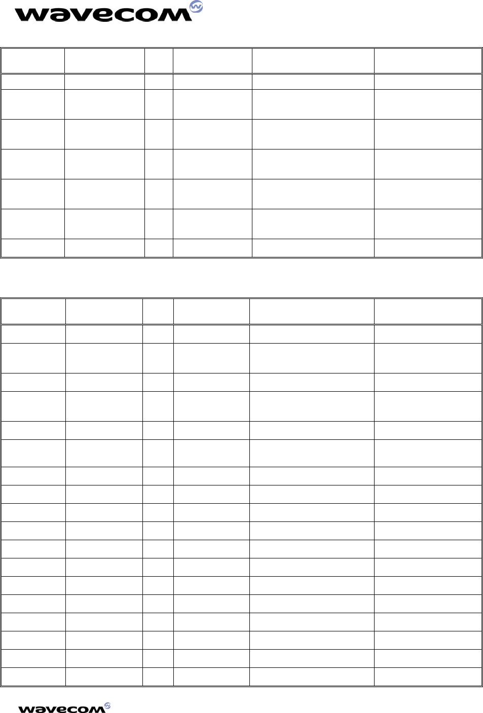
3.10 J500 connector (Auxiliary audio)
1234
J500 is a RJ9 4-pin connector.
The Table bellow gives the description of the signals of this connector.
Pin number Signal name I/O I/O type Description
1 MIC_AUX_N I Analog Auxiliary microphone negative
input
2 SPK_AUX_P O Analog Auxiliary speaker
positive output
3 SPK_AUX_N O Analog Auxiliary speaker
negative output
4 MIC_AUX_P I Analog Auxiliary microphone positive
input
confidential © Page : 27 / 42
This document is the sole and exclusive property of WAVECOM. Not to be distributed or divulged without prior written
agreement.
Ce document est la propriété exclusive de WAVECOM. Il ne peut être communiqué ou divulgué à des tiers sans son
autorisation préalable.
ERROR! REFERENCE SOURCE NOT
FOUND.P5186 USER MANUAL V 1.0
Error! Reference source not found.
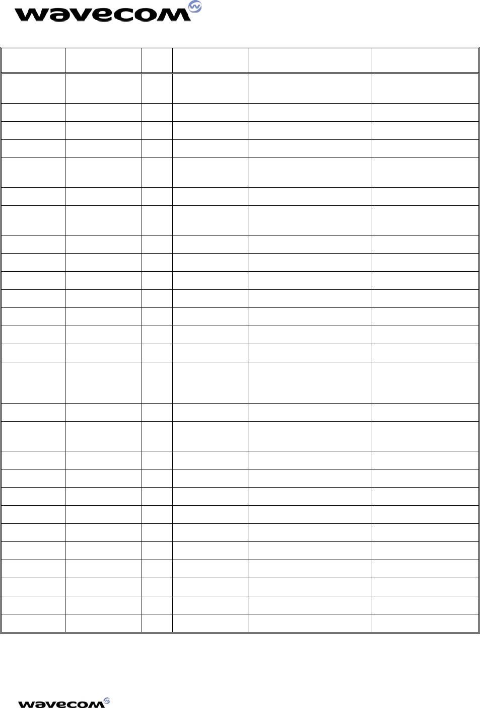
3.11 J501 connector (Main audio)
1234
J501 is a RJ9 4-pin connector.
The Table bellow gives the description of the signals of this connector.
Pin number Signal name I/O I/O type Description
MIC_N I Analog Main microphone
negative input
2 SPK_P O Analog Main speaker
positive output
3 SPK_N O Analog Main speaker
negative output
4 MIC_P I Analog Main microphone
positive input
1
confidential © Page : 28 / 42
This document is the sole and exclusive property of WAVECOM. Not to be distributed or divulged without prior written
agreement.
Ce document est la propriété exclusive de WAVECOM. Il ne peut être communiqué ou divulgué à des tiers sans son
autorisation préalable.
ERROR! REFERENCE SOURCE NOT
FOUND.P5186 USER MANUAL V 1.0
Error! Reference source not found.
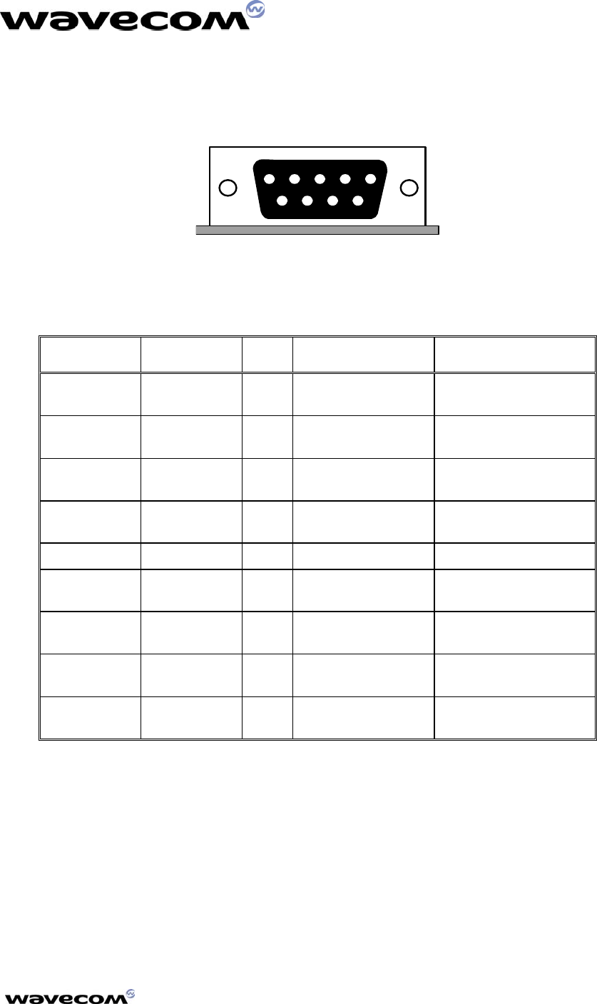
3.12 J600 connector (RS232)
12345
6789
J600 is a SUB-D 9-pin female connector. The Table bellow gives the description of the signals of
this connector.
Pin number Signal name I/O I/O type Description
1 CT109
DCD(*) O RS232
(V24/V28)
Data Carrier Detect
2 CT104
RXD
O RS232
(V24/V28)
Receive serial data
3 CT103
TXD
I RS232
(V24/V28)
Transmit serial data
4 CT108-2
DTR
I RS232
(V24/V28)
Data Terminal Ready
5 GND Ground
6 CT107
DSR
O RS232
(V24/V28)
Data Set Ready
7 CT105
RTS
I RS232
(V24/V28) Request To Send
8 CT106
CTS
O RS232
(V24/V28) Clear To Send
9 CT125
RI(*)
O RS232
(V24/V28) Ring Indicator
(*) optional signals
Note: the Wismo Pac P5186 module starter kit is a DCE (Data Communication Equipment). It can be
connected with a DTE (Data Terminal Equipment - PC or terminal) with a “straight cable”.
Warning:
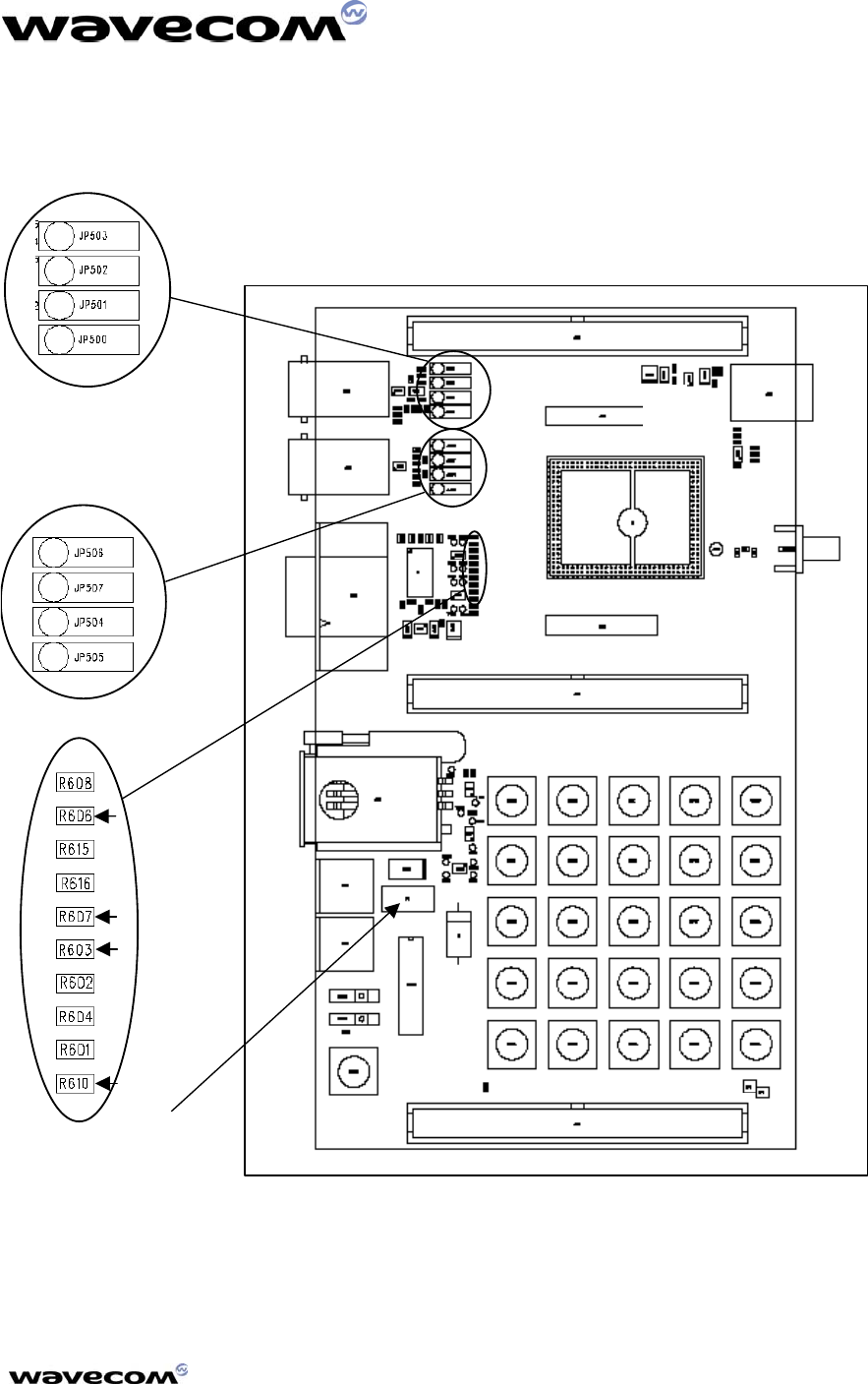
When RI and DCD signals are used by the application, the resistors R606 and R607 (0 Ω resistors) must
be placed on the mother board. A set of 0 Ω resistors is provided with the starter kit.
confidential © Page : 29 / 42
This document is the sole and exclusive property of WAVECOM. Not to be distributed or divulged without prior written
agreement.
Ce document est la propriété exclusive de WAVECOM. Il ne peut être communiqué ou divulgué à des tiers sans son
autorisation préalable.
ERROR! REFERENCE SOURCE NOT
FOUND.P5186 USER MANUAL V 1.0
Error! Reference source not found.
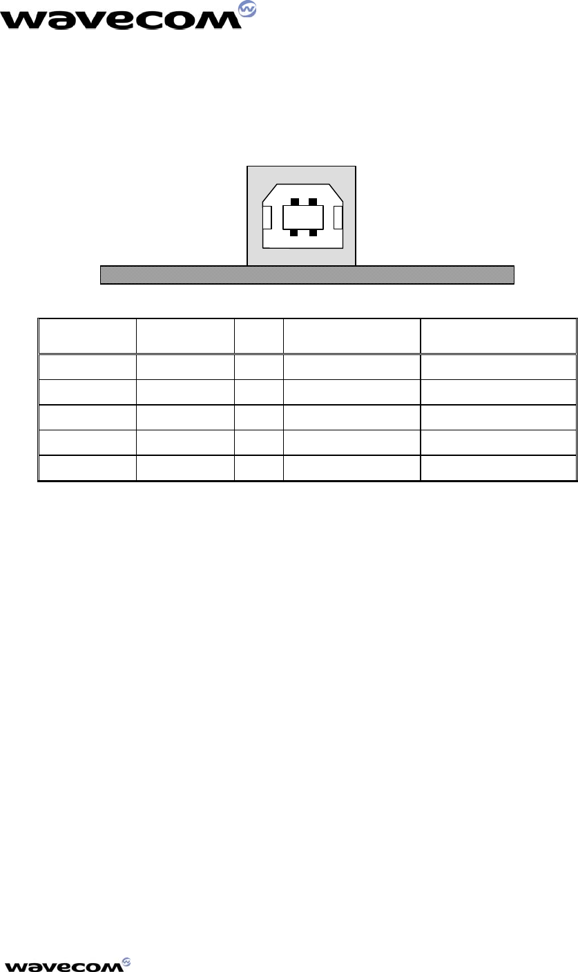
3.13 J700 connector (USB)
J700 is a USB Series B receptacle.
2
34
1
Pin number Signal name I/O I/O type Description
1 VBUS I Power supply + 5 VDC
2 DM I/O Digital USB negative line
3 DP I/O Digital USB positive line
4 GND Power supply Ground
Shell Shielding
confidential © Page : 30 / 42
This document is the sole and exclusive property of WAVECOM. Not to be distributed or divulged without prior written
agreement.
Ce document est la propriété exclusive de WAVECOM. Il ne peut être communiqué ou divulgué à des tiers sans son
autorisation préalable.
ERROR! REFERENCE SOURCE NOT
FOUND.P5186 USER MANUAL V 1.0
Error! Reference source not found.
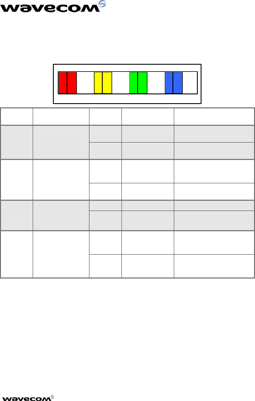
4 Operating configuration
The operating configuration is made using the SW200 switch.
1 2 3 4 5 6 7 8
Jumper Function Position
Configuration
mode Description
1 Normal DVCC supplied from J200
(VBATT)
Red
DVCC* power
supply consumption
measurement 2 Measurement DVCC supplied from J201
(5V current source)
3 Normal
Charger input (CHG_IN)
connected to J201
(5 V current source)
Yellow Charger input
management
4 Measurement Charger input (CHG_IN)
disconnected
5 Normal Shutdown inactive
Green
RS232 Serial link
transceiver
shutdown
management 6 shutdown Shutdown active
7 Modem
SIM card presence is
managed (SIM_PRES
supplied by V-core)
Blue
SIM card presence
management
(SIM_PRES**
signal) 8 Mobile
SIM card presence is not
managed (SIM_PRES not
supplied)
* DVCC is an internal digital power supply (3 V typical) mainly used as the RS232 interface power
supply.
** SIM_PRES: SIM card presence is detected via the GPIO3 of the WISMO module.
The default configuration (called “modem configuration”) of the SW200 switch is 1, 3 , 5 and 7:
Red jumper on position 1,
Yellow jumper on position 3,
Green jumper on position 5,
Blue jumper on position 7.
confidential © Page : 31 / 42
This document is the sole and exclusive property of WAVECOM. Not to be distributed or divulged without prior written
agreement.
Ce document est la propriété exclusive de WAVECOM. Il ne peut être communiqué ou divulgué à des tiers sans son
autorisation préalable.
ERROR! REFERENCE SOURCE NOT
FOUND.P5186 USER MANUAL V 1.0
Error! Reference source not found.
Consumption measurement configuration is given in the table below:
SW200 positions Measurement on external
supply input (J200)
Measurement on charger
input
(J201)
Normal mode
1 and 3 VBATT + DVCC CHG_IN
Measurement mode
2 and 4 VBATT DVCC
VBATT = WISMO module P5186 consumption.
VDCC = RS232 interface consumption.
CHG_IN = charging consumption.
The RS232 transceiver shutdown function (SW200 positions 5 and 6) is used for serial link
consumption measurement (DVCC) and test of the RS232 cable.
confidential © Page : 32 / 42
This document is the sole and exclusive property of WAVECOM. Not to be distributed or divulged without prior written
agreement.
Ce document est la propriété exclusive de WAVECOM. Il ne peut être communiqué ou divulgué à des tiers sans son
autorisation préalable.
ERROR! REFERENCE SOURCE NOT
FOUND.P5186 USER MANUAL V 1.0
Error! Reference source not found.
5 Functional description
5.1 Power supply
J200 is the Power Supply connector of the WISMO module. The voltage applied to this connector is
described hereafter.
Minimum Typical Maximum
VBATT+ 3.3 V 4.2 V
5.2 Charger function
J201 is used to simulate a charger. The voltage applied to this connector is described hereafter.
Minimum Typical Maximum
CHG_IN 4.8 V 5.2 V
Note: CHG_IN current = 800 mA max.
5.3 SIM function
The SIM interface controls 3 V SIM cards.
Note: in a future version of the starter kit, the use of 1.8 V SIM cards will be available.
When the SIM_PRES signal is used by the application (detection of SIM card presence) then a
jumper must be set on position 7 of the SW200 switch.
When the SIM_PRES signal is not used by the application, then a jumper must be set on position 8
of the SW200 switch.
confidential © Page : 33 / 42
This document is the sole and exclusive property of WAVECOM. Not to be distributed or divulged without prior written
agreement.
Ce document est la propriété exclusive de WAVECOM. Il ne peut être communiqué ou divulgué à des tiers sans son
autorisation préalable.
ERROR! REFERENCE SOURCE NOT
FOUND.P5186 USER MANUAL V 1.0
Error! Reference source not found.
5.4 RS232 function
5.4.1 Introduction
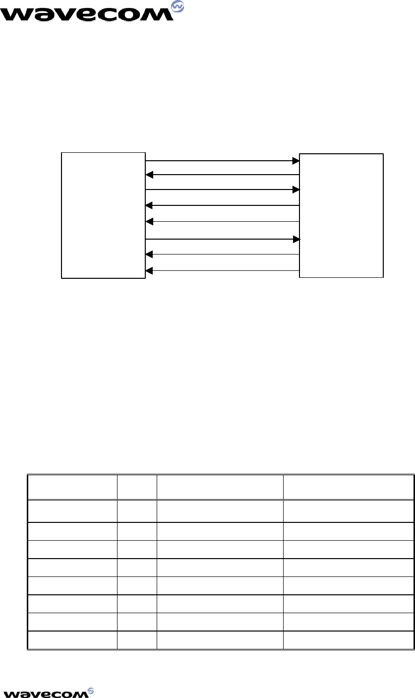
The Starter Kit is fitted with a MAX3238 RS232 transceiver device (U1).
The Starter Kit acts as a DCE (Data Communication Equipment) and is connected to a DTE (Data
Terminal Equipment - PC or terminal) with a “straight cable”.
DTE
Starter
Kit
(DCE)
CT103 / TX
CT108-2 / DTR
CT105 / RTS
CT104 / RX
CT106 / CTS
CT107 / DSR
CT109 / DCD
CT125 / RI
Figure 1: RS232 serial link
RS232 link default configuration is made of 6 wires: TX, RX, CTS, RTS, DTR and DSR.
Warning:
When RI and DCD signals are used by the application, the resistors R606 and R607 (0 Ω resistors) must
be placed on the mother board. In the mother board default configuration, these resistors are not
placed. So, a set of 0 Ω resistors is provided with the starter kit.
When the SPI2 bus of the WISMO P5186 module is used, resistors R603 and R610 must be unsoldered
and removed from the motherboard, because the SPI2 bus signals (SPI2_DATA and SPI2_CLK) are
multiplexed with DSR1 and DTR1. In that case, the RS232 serial link will be make up of 4 wires only: TX,
RX, CTS and RTS.
The signal name relashionship between the WISMO Pac P5186 serial interface (V24/CMOS) and
the RS232 interface (V24/V28) is given hereafter:
Pin # I/O RS2332 signal P5186 signal
1 O DCD GPIO7
2 O RXD TXD1
3 I TXD RXD1
4 I DTR DSR1
6 O DSR DTR1
7 I RTS CTS
8 O CTS RTS
9 O RI GPIO6
confidential © Page : 34 / 42
This document is the sole and exclusive property of WAVECOM. Not to be distributed or divulged without prior written
agreement.
Ce document est la propriété exclusive de WAVECOM. Il ne peut être communiqué ou divulgué à des tiers sans son
autorisation préalable.
ERROR! REFERENCE SOURCE NOT
FOUND.P5186 USER MANUAL V 1.0
Error! Reference source not found.
5.4.2 Shutdown of Max3238
The Max3238 device can be shut down using the switch SW200:
Position 5: shut down inactive,
Position 6: shut down active.
When the shut down is active, the MAX3238 device transmitters and receivers are disabled and their
outputs go high impedance.
The shutdown is used for measuring the serial link consumption and for testing the RS232 cable.
5.5 Audio functions
When Auxiliary Audio interface is used on the mother board, the following jumpers must be
connected between pin 2 an pin 3:
JP500 and JP501: auxiliary speaker,
JP502 and JP503: auxiliary microphone.
When Main Audio interface is used on the mother board, the following jumpers must be connected
between pin 2 and pin 3:
JP504 and JP505: main speaker,
JP506 and JP507: main microphone.
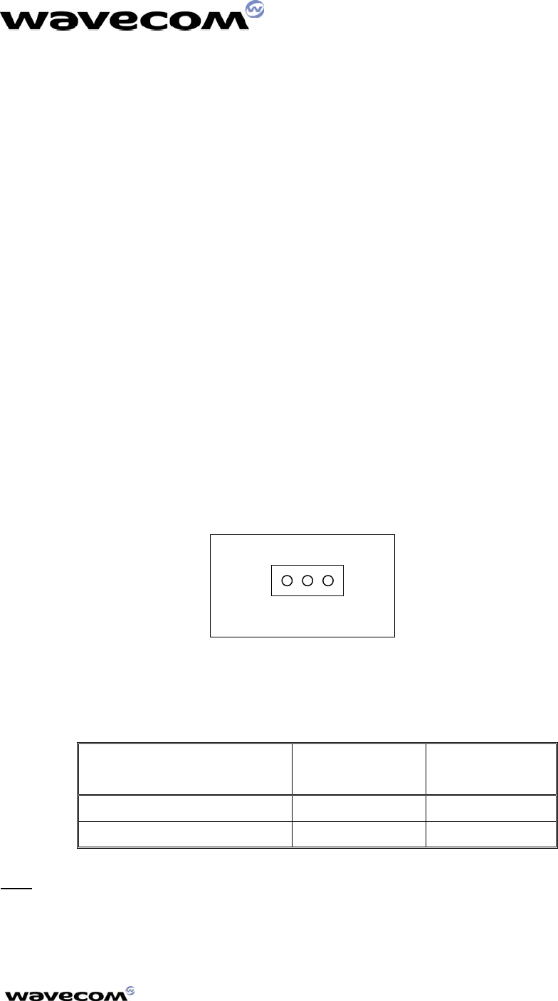
1 2 3
JP500 to JP507
5.6 ON/~OFF and BOOT function
Mode BOOT
(SW202)
ON/~OFF
(SW201)
Normal OFF ON
Download ON ON
Note: internal boot is started when both switches SW202 (BOOT) and SW201 (ON/~OFF) are ON
during the reset of the module (SW203).
confidential © Page : 35 / 42
This document is the sole and exclusive property of WAVECOM. Not to be distributed or divulged without prior written
agreement.
Ce document est la propriété exclusive de WAVECOM. Il ne peut être communiqué ou divulgué à des tiers sans son
autorisation préalable.
ERROR! REFERENCE SOURCE NOT
FOUND.P5186 USER MANUAL V 1.0
Error! Reference source not found.
5.7 RESET function
When SW203 is pressed (RESET button), the WISMO module is reset.
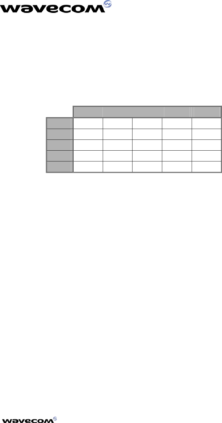
5.8 KEYPAD function
The following table shows the matrix of the keyboard:
COL0 COL1 COL2 COL3 COL4
ROW0 SW400 SW405 SW410 SW415 SW420
ROW1 SW401 SW406 SW411 SW416 SW421
ROW2 SW402 SW407 SW412 SW417 SW422
ROW3 SW403 SW408 SW413 SW418 SW423
ROW4 SW404 SW409 SW414 SW419 SW424
Example: If you press the key SW412, an electric detection will be made on ROW2 and COL2.
5.9 Antenna function
The antenna is connected to the board via the SMA300 connector.
The antenna cable is fitted with a FME connector and a SMA/FME adaptator is supplied to permit
the connection to the board.
5.10 ESD protections
External ESD protections are added on the mother board for the following signals:
WISMO Pac P5186 VBATT and CHG_IN input signals.
WISMO Pac P5186 /RESET and BOOT input signals.
WISMO Pac P5186 SIM interface signals: SIM_PRES, SIM_VCC, SIM_IO, SIM_CLK,
SIM_RST,
WISMO Pac P5186 Serial link signals (UART1): TXD1, RTS1, DTR1, DSR1, RXD1,
CTS1, RI1 (GPIO6) and DCD1 (GPIO7).
Main audio interface signals.
Auxiliary audio interface signals.
confidential © Page : 36 / 42
This document is the sole and exclusive property of WAVECOM. Not to be distributed or divulged without prior written
agreement.
Ce document est la propriété exclusive de WAVECOM. Il ne peut être communiqué ou divulgué à des tiers sans son
autorisation préalable.

ERROR! REFERENCE SOURCE NOT
FOUND.P5186 USER MANUAL V 1.0
Error! Reference source not found.
6 Getting started
6.1 Procedure
Make sure that both the “ON/OFF” switch (SW201) and “BOOT” switch (SW202) are on
position “OFF”.
Put the operating configuration switch (SW200) in default configuration position:
o Red jumper on position 1,
o Yellow jumper on position 3,
o Green jumper on position 5,
o Blue jumper on position 7.
Make sure that the jumpers JP500 to JP507 are connected between pin 2 and pin 3 (Main
audio interface and auxiliary audio interface).
Make sure that the external DC power supply is switched off and connect it to J200 (VBATT)
using the power supply cable provided with the starter kit.
Connect the RS232 cable, provided with the starter kit, between port COM1 (or COM2) of
the PC and J600 of the board.
The COM port properties must be the following:
- Bits per second: 115.200 k,
- Data bits: 8,
- Parity: None,
- Stop bits: 2,
- Flow control: None.
Connect the antenna to the SMA300 connector (if communications are required).
Connect the handset, provided with the starter kit, to the Main Audio connector J500 (if
communications are required).
Insert a SIM card into the SIM card holder (if communications are required).
Switch on the external power supply then adjust:
o the output voltage to 4 Volts DC,
o the current limitation to 2 A min.
Switch “ON” the “ON/OFF” switch (SW201) of the board then check there is a consumption
on the external power supply amperemeter.
On the PC, open a terminal emulator window to communicate with the WISMO module via
the COM1 (or COM2) port.
Press the “RESET” key (SW203) to reset the WISMO module.
Using the terminal emulator, send the following command on COM port to communicate with
the WISMO module: AT↵.
When the communication is established between the PC and the WISMO module, the last
one sends the message “OK” as a reply. This message is displayed in the terminal
emulator window.
confidential © Page : 37 / 42
This document is the sole and exclusive property of WAVECOM. Not to be distributed or divulged without prior written
agreement.
Ce document est la propriété exclusive de WAVECOM. Il ne peut être communiqué ou divulgué à des tiers sans son
autorisation préalable.

ERROR! REFERENCE SOURCE NOT
FOUND.P5186 USER MANUAL V 1.0
Error! Reference source not found.
6.2 Trouble shooting
If I=0 on the external power supply amperemeter, then:
o Check that the external power supply:
Is “ON”.
is connected on J200.
is adjusted for an output voltage between 3.2 V and 4.2 V.
o Check that the “ON/OFF” switch (SW201) is “ON”.
o Check the fuse F1 (3 A) and replace it if necessary.
Note: technical characteristics of the fuse to be replaced are given in appendix.
o Check the configuration of the jumpers on switch SW200.
If the WISMO module does not reply to the “AT↵” command (no message “OK” is
received), make sure that:
o The WISMO module is present on the mother board (socket up mounted).
o a software has been loaded in the module (refer to the documentation [3]).
6.3 Safety, FCC and Industry of Canada Regulatory compliance
6.3.1 RF safety
6.3.1.1 General
Your GSM terminal1 is based on the GSM standard for cellular technology. The GSM standard is
spread all over the world. It covers Europe, Asia and some parts of America and Africa. This is the
most used telecommunication standard.
Your GSM terminal is actually a low power radio transmitter and receiver. It sends out and receives
radio frequency energy. When you use your GSM application, the cellular system which handles
your calls controls both the radio frequency and the power level of your cellular modem.
6.3.1.2 Exposure to RF energy
There has been some public concern about possible health effects of using GSM terminals.
Although research on health effects from RF energy has focused on the current RF technology for
many years, scientists have begun research regarding newer radio technologies, such as GSM.
After existing research had been reviewed, and after compliance to all applicable safety standards
had been tested, it has been concluded that the product was fitted for use.
If you are concerned about exposure to RF energy there are things you can do to minimize
exposure. Obviously, limiting the duration of your calls will reduce your exposure to RF energy. In
addition, you can reduce RF exposure by operating your cellular terminal efficiently by following the
below guidelines.
confidential © Page : 38 / 42
This document is the sole and exclusive property of WAVECOM. Not to be distributed or divulged without prior written
agreement.
Ce document est la propriété exclusive de WAVECOM. Il ne peut être communiqué ou divulgué à des tiers sans son
autorisation préalable.
1 based on WISMO2D

ERROR! REFERENCE SOURCE NOT
FOUND.P5186 USER MANUAL V 1.0
Error! Reference source not found.
6.3.1.3 Efficient terminal operation
For your GSM terminal to operate at the lowest power level, consistent with satisfactory call quality:
• If your terminal has an extendible antenna, extend it fully. Some models allow you to place a
call with the antenna retracted. However your GSM terminal operates more efficiently with
the antenna fully extended.
• Do not hold the antenna when the terminal is « IN USE ». Holding the antenna affects call
quality and may cause the modem to operate at a higher power level than needed.
6.3.2 Modular Transmitter
Modular transmitter. This device is to be used only for mobile and fixed applications.
The antenna(s) used for this transmitter must be installed to provide a separation distance of
at least 20 cm from all persons and must not be co-located or operating in conjunction with
any other antenna or transmitter. The antenna(s) used for this transmitter must not exceed
a gain of 3 dBi for mobile operation and 7 dBi for fixed operation. Users and OEM
integrators must be provided with antenna installation instructions and transmitter operating
conditions for satisfying RF exposure compliance. OEM must also be provided with
labelling instructions. This device contains 900 MHz GSM functions that are not operational
in U.S. Territories. This filing is only applicable for GSM 850 MHz and 1900 MHz PCS
operations.
This device complies with Part 15 of the FCC Rules. Operation is subject to the following two conditions: (1)
this device may not cause harmful interference, and (2) this device must accept any interference received,
including interference that may cause undesired operation.
Your mobile device is a low power radio transmitter and receiver. When it is ON, it receives and also sends
out radio frequency (RF) signals. In August 1996, the Federal Communications Commission (FCC) adopted
RF exposure guidelines with safety levels for mobile device. Those guidelines are consistent with safety
standards previously set by both U.S. and international standards bodies: American National Standard Institute
(ANSI), National Council of Radiation Protection and Measurements (NCRP), and International Commission
on Non-Ionizing Radiation Protection (ICNRP). Those standards were based on comprehensive and periodic
evaluations of the relevant scientific literature. The design of your Module complies with the FCC guidelines
and applicable
WARNING: Unauthorized antennas, modifications, or attachments could impair call quality, damage
the Module, or result in violation of FCC regulations. Do not use the Module with a damaged antenna.
Please contact your local authorized dealer for antenna replacement.
Important!
Read these safety guidelines prior to using your Module. Failure to follow these rules and guidelines may be
dangerous and/or illegal.
6.3.3 Road Safety Information
Do not use a hand-held Module while driving a vehicle. Talking on the Module while driving is dangerous and
illegal in some locations. If using a hand-held Module, park the vehicle before conversing. Remember – road
safety always comes first!
confidential © Page : 39 / 42
This document is the sole and exclusive property of WAVECOM. Not to be distributed or divulged without prior written
agreement.
Ce document est la propriété exclusive de WAVECOM. Il ne peut être communiqué ou divulgué à des tiers sans son
autorisation préalable.

ERROR! REFERENCE SOURCE NOT
FOUND.P5186 USER MANUAL V 1.0
Error! Reference source not found.
6.3.4 Aircraft Safety Information
Power down your Module prior to boarding an aircraft. Sending and receiving calls on your Module on an
aircraft is prohibited by law and aviation regulations. Using a wireless Module in an aircraft may interfere with
aircraft radio communication or navigation equipment, and disrupt the wireless Module network. When
boarding an aircraft, turn your Module OFF.
6.3.5 Hospital & Medical Safety Information
Power down your Module prior to entering hospitals, health care facilities, or when near medical equipment.
Operating any radio transmitting equipment, including digital wireless Modules, may interfere with RF-
sensitive medical devices. Follow all posted regulations while in hospitals and health care facilities regarding
the use of your Module.
6.3.6 Blasting and Refueling Safety Information
Do not use your Module near a blasting site. Power down your Module when in any area with a potentially
explosive
Atmosphere. Radio transmissions in such areas could cause an explosion or fire, resulting in bodily injury or
even death. Obey all posted signs and instructions regarding the use of wireless Module usage. Observe
restrictions on the use of radio equipment in fuel depots (fuel storage and distribution areas), chemical plants
or where blasting operations are in progress.
6.3.7 Interference Safety Information
All mobile Modules are subject to radio frequency interference that may affect the performance of your
Module. Your digital wireless Module is a low power radio transmitter and receiver. The design of your
Module complies with the FCC guidelines and applicable standards. Never rely solely on your Module for
essential communications (e.g., medical emergencies). You must be in a service area with adequate signal
strength to use the Module. Emergency calls may not be possible on all wireless Module networks or when
certain network services and/or Module features are in use. Check with your local service provider(s).
6.3.8 Service Safety Information
Only qualified service personnel are authorized to repair your digital wireless Module and equipment. Use
only approved accessories. Contact you sales representative authorized service centers.
FCC RF EXPOSURE INFORMATION
In August 1996 the Federal Communications Commission (FCC) of the United States with its action in Report
and Order FCC 96-326 adopted an updated safety standard for human exposure to radio frequency
electromagnetic energy emitted by FCC regulated transmitters. Those guidelines are consistent with the safety
standard previously set by both U.S. and international standards bodies. The design of this phone complies
with the FCC guidelines and these international standards.
For more information about RF exposure, please visit the FCC website at www.fcc.gov
confidential © Page : 40 / 42
This document is the sole and exclusive property of WAVECOM. Not to be distributed or divulged without prior written
agreement.
Ce document est la propriété exclusive de WAVECOM. Il ne peut être communiqué ou divulgué à des tiers sans son
autorisation préalable.

ERROR! REFERENCE SOURCE NOT
FOUND.P5186 USER MANUAL V 1.0
Error! Reference source not found.
6.3.9 Federal Communications Commission (FCC) Notice
This equipment has been tested and found to comply with the limits for a class B digital device, pursuant to
part 15 of the FCC Rules. These limits are designed to provide reasonable protection against harmful
interference in a residential installation. This equipment generates, uses, and can radiate radio frequency
energy.
If not installed and used in accordance with the instructions, it may cause harmful interference to radio or
television reception, which can be determined by turning the equipment off and on. The user is encouraged to
try to correct the interference by one or more of the following measures:
• Reorient or relocate the receiving antenna.
• Increase the distance between the equipment and the receiver.
• Connect the equipment to an outlet on a circuit different from the outlet where the receiver is
connected.
• Consult the dealer or an experienced radio/TV technician for assistance
confidential © Page : 41 / 42
This document is the sole and exclusive property of WAVECOM. Not to be distributed or divulged without prior written
agreement.
Ce document est la propriété exclusive de WAVECOM. Il ne peut être communiqué ou divulgué à des tiers sans son
autorisation préalable.
ERROR! REFERENCE SOURCE NOT
FOUND.P5186 USER MANUAL V 1.0
Error! Reference source not found.
confidential © Page : 42 / 42
This document is the sole and exclusive property of WAVECOM. Not to be distributed or divulged without prior written
agreement.
Ce document est la propriété exclusive de WAVECOM. Il ne peut être communiqué ou divulgué à des tiers sans son
autorisation préalable.
7 Appendix