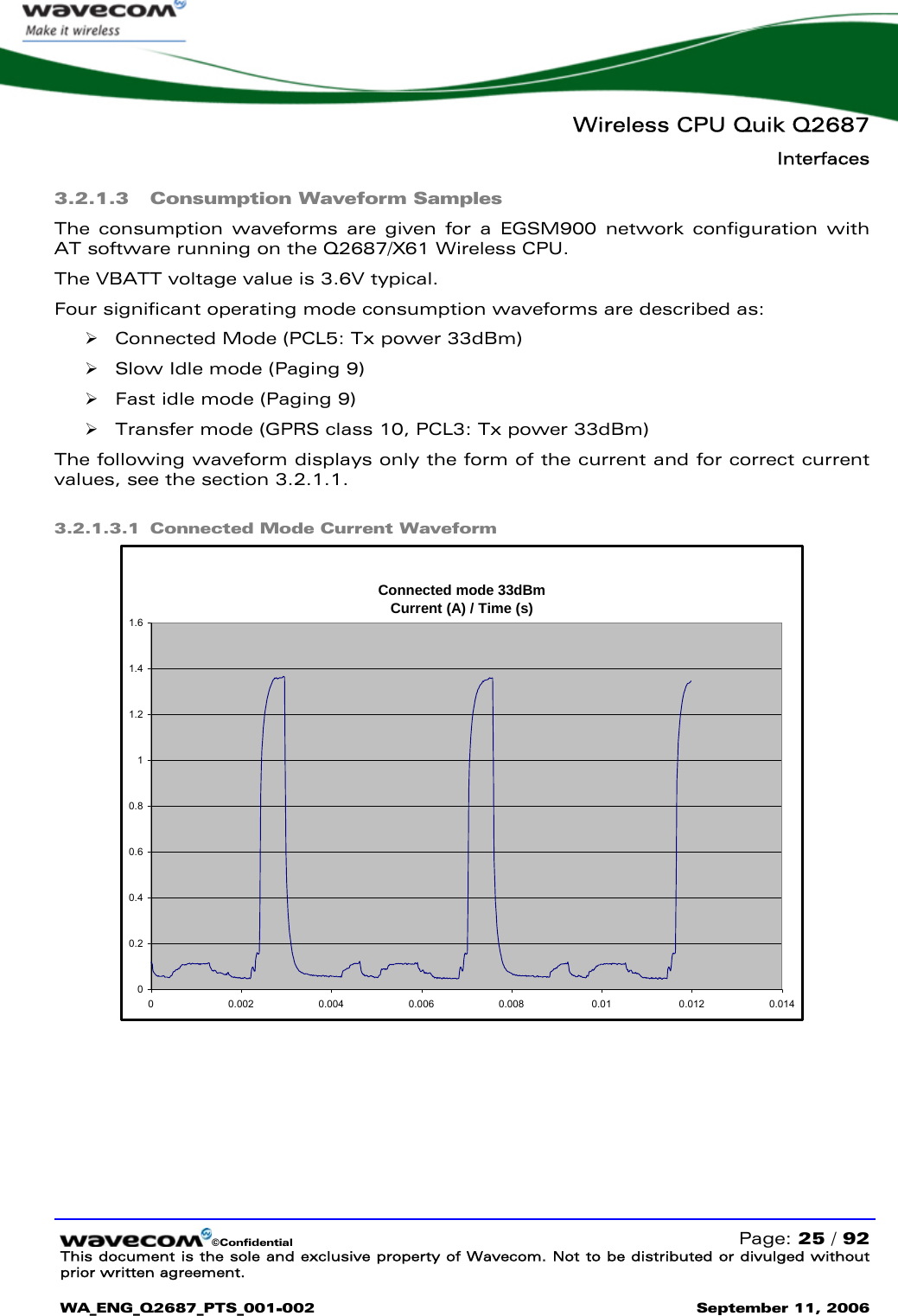
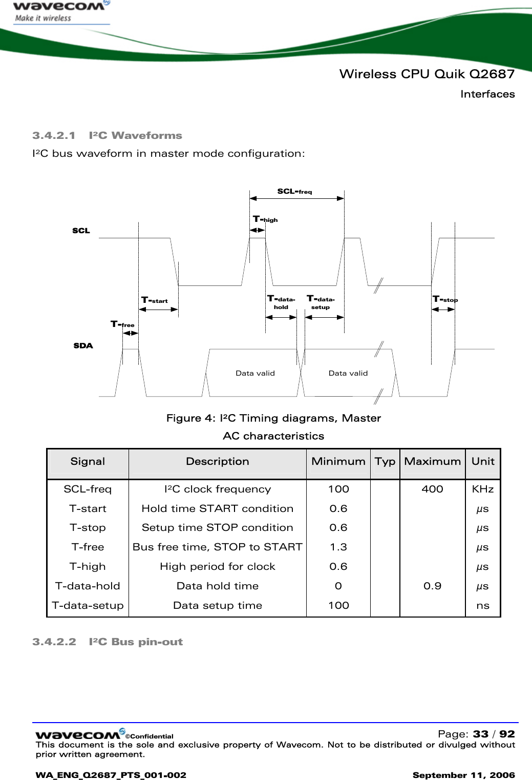
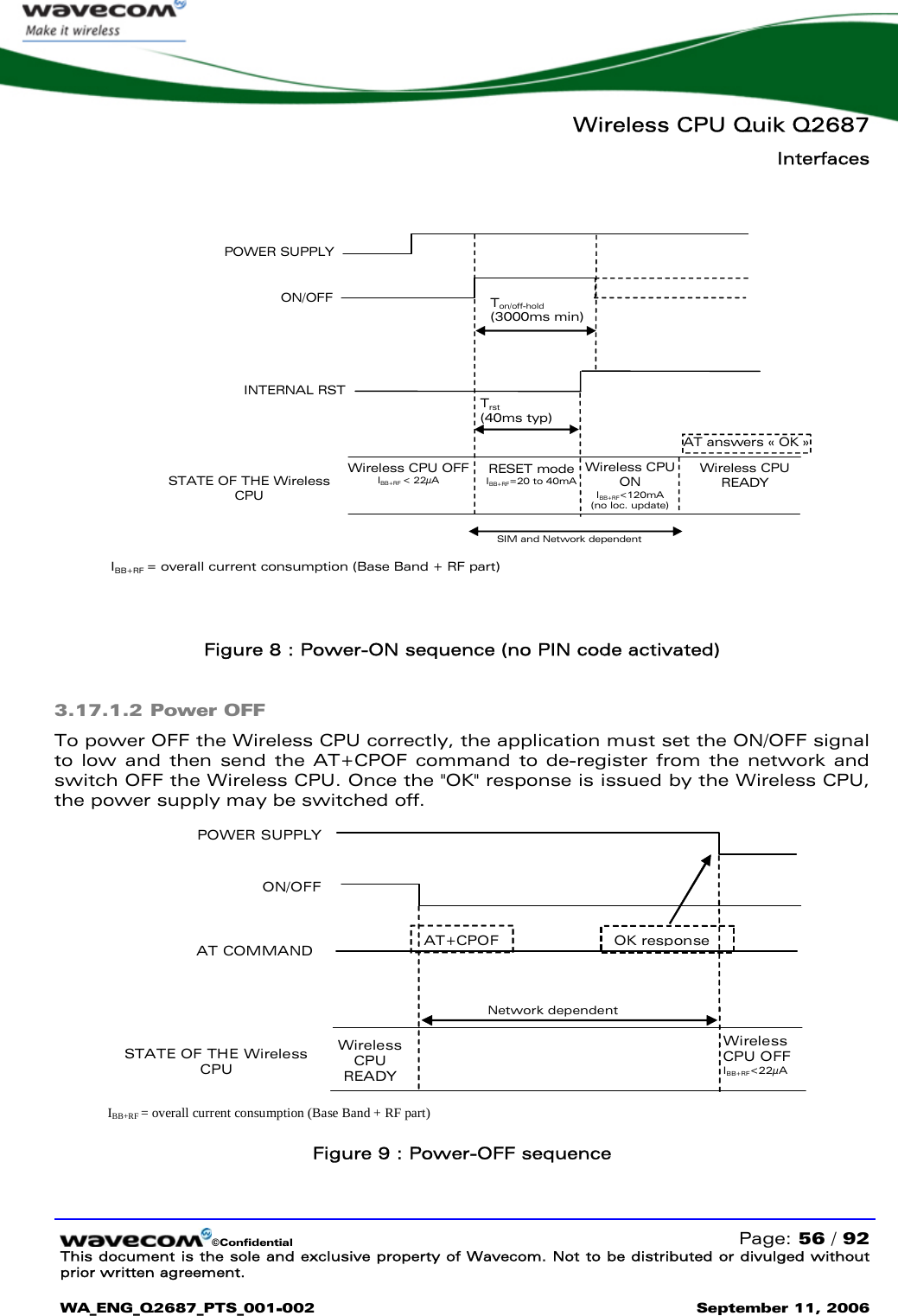
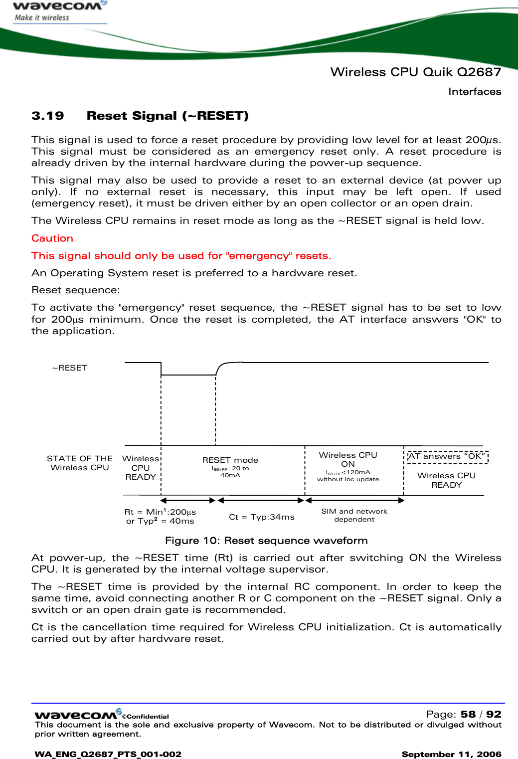
Sierra Wireless Q2687 Wireless CPU (850/900/1800/1900 MHz) User Manual Q2687 PTS rev002
Sierra Wireless, Inc. Wireless CPU (850/900/1800/1900 MHz) Q2687 PTS rev002
UserManual.wiki
>
Sierra Wireless
>
Q2687 User Manual
>
User Manual
Contents
1.
User Manual
2.
Users Manual
User Manual
Navigation menu
Upload a User Manual
Namespaces
Wiki Guide
HTML
PDF
Info
Views
User Manual
Discussion / Help
Navigation
![Wireless CPU Quik Q2687 References ©Confidential Page: 11 / 92 This document is the sole and exclusive property of Wavecom. Not to be distributed or divulged without prior written agreement. WA_ENG_Q2687_PTS_001-002 September 11, 2006 1 References 1.1 Reference Documents For more details, several reference documents may be consulted. The Wavecom reference documents are provided in the Wavecom documents package, contrary to the general reference documents which are not authored by Wavecom. 1.1.1 Wavecom Reference Documents [1] Automotive Environmental Control Plan for Q2687 Wireless CPU WM_QUA_Q2687_DCP_001 [2] Q2687 Wireless CPU Customer Design Guidelines WM_DEV_Q2687_PTS_007 [3] Q2687 Wireless CPU Process Customer Guidelines WM_PRJ_Q2686_PTS_004 [4] AT Commands Interface Guide for OS 6.61 WM_DEV_OAT_UGD_014 1.1.2 General Reference Document [5] "I²C Bus Specification", Version 2.0, Philips Semiconductor 1998 [6] ISO 7816-3 Standard 1.2 List of abbreviations Abbreviations Definition AC Alternating Current ADC Analog to Digital Converter A/D Analog to Digital conversion AF Audio-Frequency AT ATtention (prefix for modem commands) AUX AUXiliary CAN Controller Area Network CB Cell Broadcast](https://usermanual.wiki/Sierra-Wireless/Q2687.User-Manual/User-Guide-725678-Page-11.png)
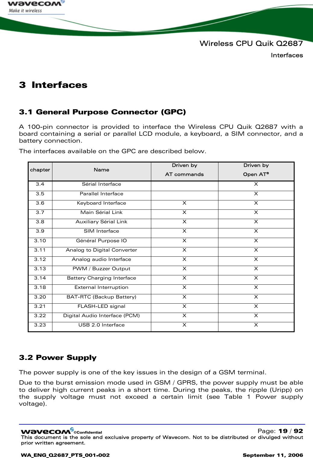

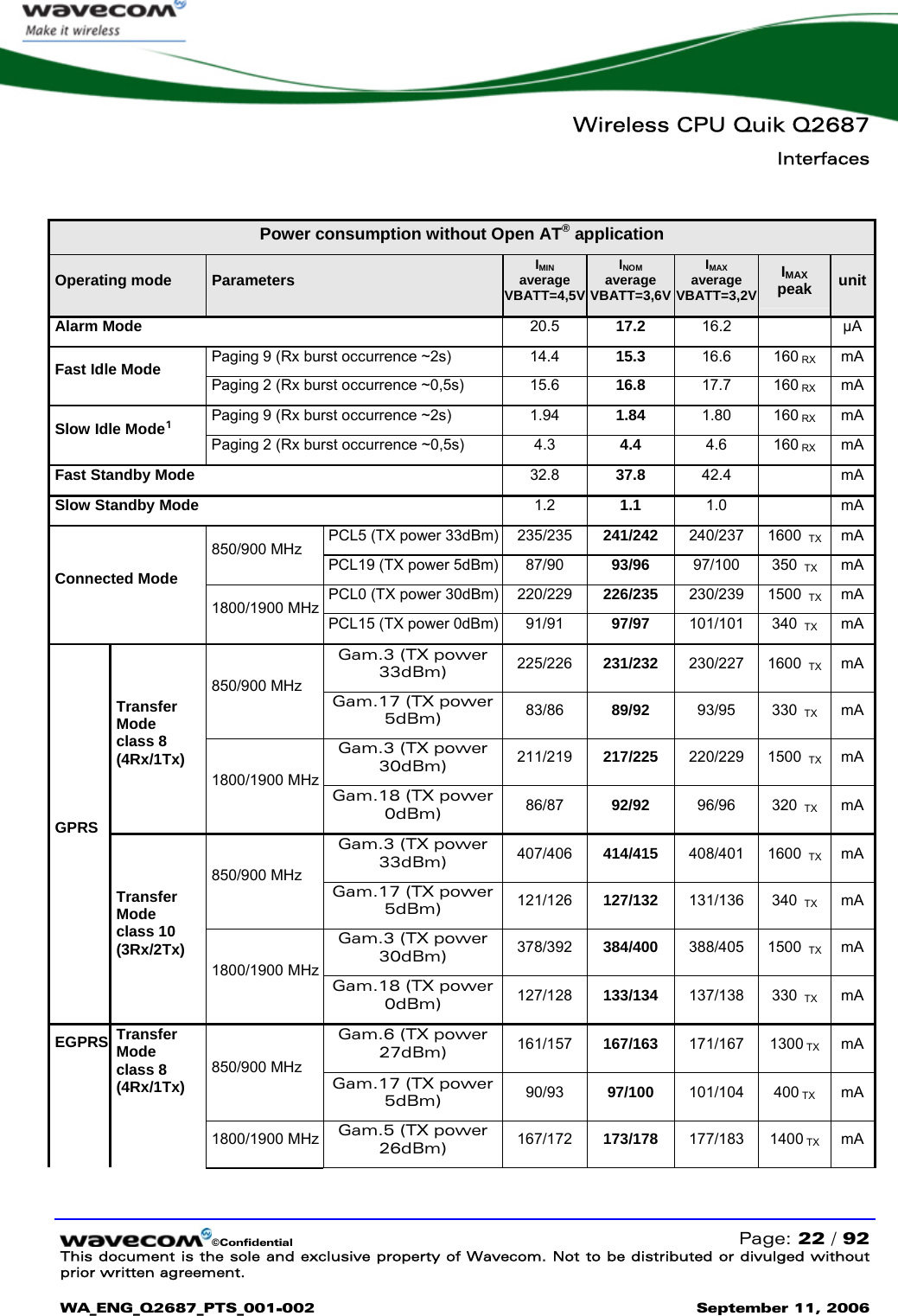
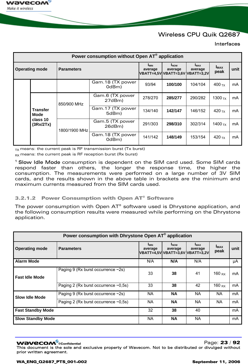
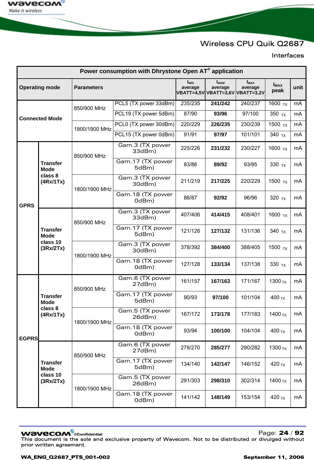
![Wireless CPU Quik Q2687 Interfaces ©Confidential Page: 21 / 92 This document is the sole and exclusive property of Wavecom. Not to be distributed or divulged without prior written agreement. WA_ENG_Q2687_PTS_001-002 September 11, 2006 (1): This value has to be maintained during the burst (with 2.0A Peak in GSM, GPRS or EGPRS mode) (2): The maximum operating Voltage Stationary Wave Ratio (VSWR) is 2:1 When supplying the Wireless CPU from a battery, the total impedance (battery + protections + PCB) should be <150 mOhms. Caution: When the Wireless CPU is in Alarm mode, no voltage must be applied on any pin of the 100-pin connector except on BAT-RTC (pin 7) for RTC operation or ON/~OFF (pin 19) to power ON the Wireless CPU. 3.2.1 Power Consumption Power consumption is dependent on the configuration used. It is for this reason that the following consumption values are given for each mode, RF band and type of software used (AT or Open AT™). All the following information is given assuming a 50 Ω RF output. The following consumption values were obtained by performing measurements on Wireless CPU samples at a temperature of 25° C. Three VBATT values are used to measure the consumption, VBATTmin (3.2V), VBATTmax (4.5V) and VBATTtyp (3.6V). The average current is given for the three VBATT values and the peak current given is the maximum current peak measured with the three VBATT voltages. For a more detailed description of the operating modes, see the Appendix of the AT Command Interface Guide OS 6.61 [4] For more information about the consumption measurement procedure, see Wireless CPU Quik Q2687 Customer Design Guidelines [2]. 3.2.1.1 Power Consumption without Open AT® Processing The following measurement results are relevant only when: ¾ There is no Open AT® application ¾ The Open AT® application is disabled ¾ No processing is required by the Open AT® application](https://usermanual.wiki/Sierra-Wireless/Q2687.User-Manual/User-Guide-725678-Page-21.png)
![Wireless CPU Quik Q2687 Interfaces ©Confidential Page: 34 / 92 This document is the sole and exclusive property of Wavecom. Not to be distributed or divulged without prior written agreement. WA_ENG_Q2687_PTS_001-002 September 11, 2006 Pin description Signal Pin number I/O I/O type Reset state Description Multiplexed with SCL 44 O Open drain Z Serial Clock GPIO26 SDA 46 I/O Open drain Z Serial Data GPIO27 See section 3.3, "Electrical information for digital I/O" for Open drain, 2V8 and 1V8 voltage characteristics and Reset state definition. 3.5 Parallel Interface The Wireless CPU Quik Q2687 offers a 16-bit wide parallel bus interface. Few signals are multiplexed. It is possible to have these configurations. For software information, see the document [4]. • CS3*, A1, GPIO1, GPIO2 • CS3*, A1, A24, GPIO1 • CS3*, A1, A24, A25 • CS3*, CS2*, A1, GPIO2 • CS3*, CS2*, A1, A24](https://usermanual.wiki/Sierra-Wireless/Q2687.User-Manual/User-Guide-725678-Page-34.png)
![Wireless CPU Quik Q2687 Interfaces ©Confidential Page: 38 / 92 This document is the sole and exclusive property of Wavecom. Not to be distributed or divulged without prior written agreement. WA_ENG_Q2687_PTS_001-002 September 11, 2006 3.8 Auxiliary Serial Link (UART2) The Bluetooth application on auxiliary serial interface (UART2) is available on Wireless CPU Quik Q2687 product. See the Application Note WM_ASW_AOT_APN_016 and the document [4]. Pin description of UART2 interface Signal Pin number I/O I/O type Reset state Description Multiplexed with CT103 / TXD2* 31 I 1V8 Z Transmit serial data GPIO14 CT104 / RXD2* 30 O 1V8 Z Receive serial data GPIO15 ~CT106 / CTS2* 32 O 1V8 Z Clear To Send GPIO16 ~CT105 / RTS2* 33 I 1V8 Z Request To Send GPIO17 See Section 3.3, "Electrical information for digital I/O" for Open drain, 2V8 and 1V8 voltage characteristics and Reset state definition. * According to PC view The Q2687 is designed to operate using all the serial interface signals. In particular, it is mandatory to use RTS and CTS for hardware flow control in order to avoid data corruption during transmission. The maximum baud rate of UART2 is 115 Kbit/s. 3.9 SIM Interface The Subscriber Identification Module (SIM) may be directly connected to the Wireless CPU Quik Q2687 via this dedicated interface. 3.9.1 General Description The five signals are: • SIM-VCC: SIM power supply • ~SIM-RST: reset • SIM-CLK: clock • SIM-IO: I/O port • SIMPRES: SIM card detect The SIM interface controls a 3V/1V8 SIM. This interface is fully compliant with the GSM 11.11 recommendations related to SIM functions.](https://usermanual.wiki/Sierra-Wireless/Q2687.User-Manual/User-Guide-725678-Page-38.png)
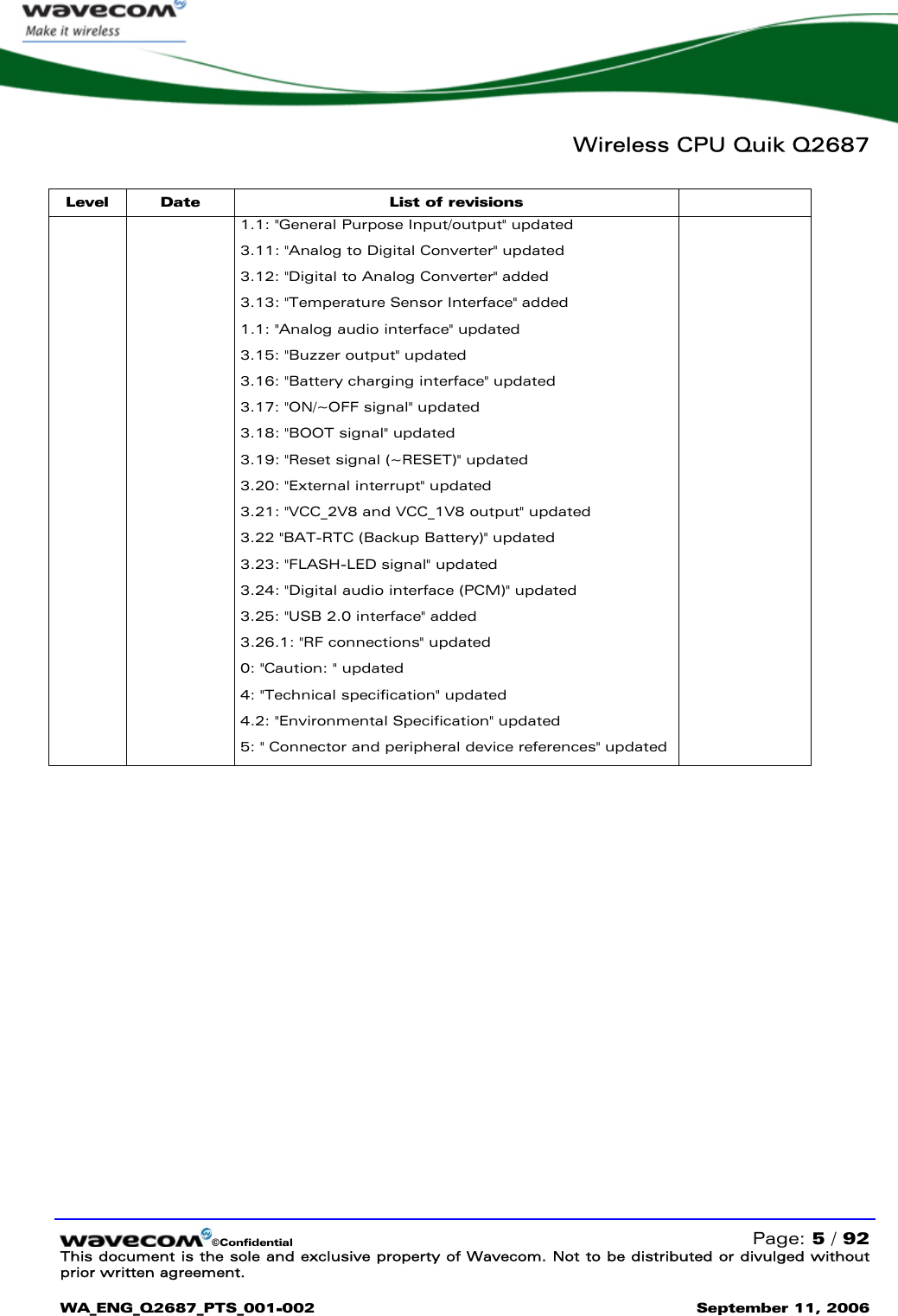
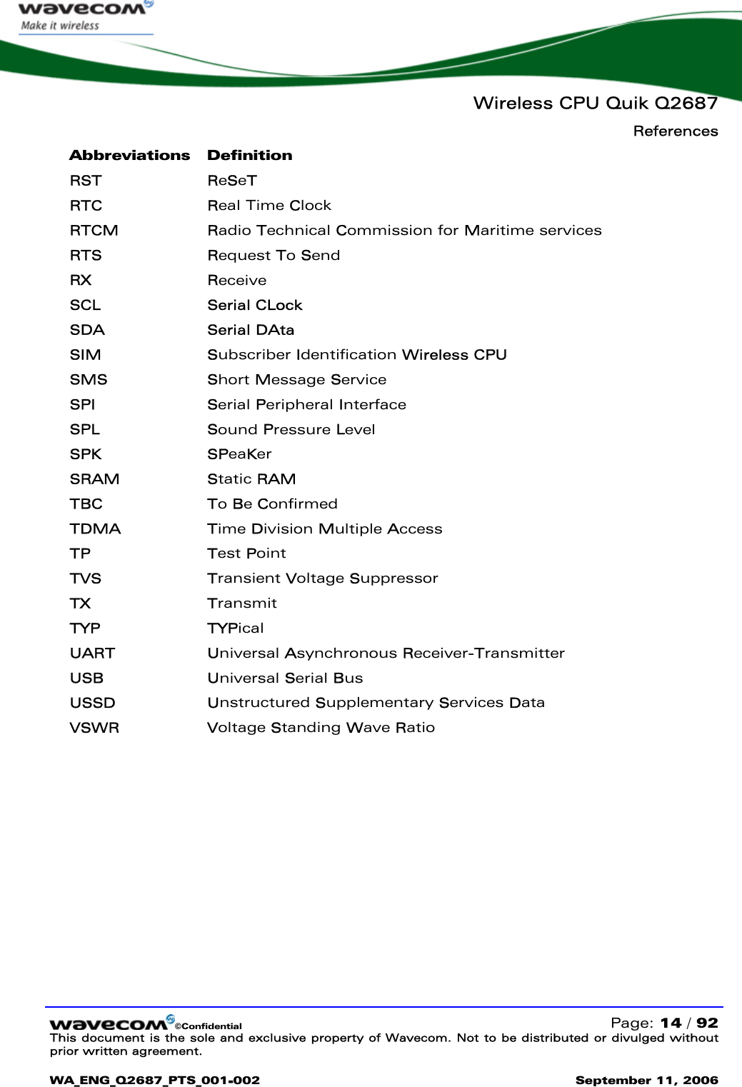
![Wireless CPU Quik Q2687 Interfaces ©Confidential Page: 45 / 92 This document is the sole and exclusive property of Wavecom. Not to be distributed or divulged without prior written agreement. WA_ENG_Q2687_PTS_001-002 September 11, 2006 3.13 Temperature Sensor Interface A temperature sensor is implanted in the Q2687 Wireless CPU. The software may inform (via an ADC) the temperature in the Q2687 Wireless CPU. The following waveform describes the characteristic of this function. For more details, see the document [4]. The average step is 15mV / °C. Characteristic of the Temperature Sensor00,20,40,60,811,21,41,61,82-50 -40 -30 -20 -10 0 10 20 30 40 50 60 70 80 90 100Temperature (°C)Voltage (V) Figure 5: Characteristics of the Temperature Sensor](https://usermanual.wiki/Sierra-Wireless/Q2687.User-Manual/User-Guide-725678-Page-45.png)
![Wireless CPU Quik Q2687 Interfaces ©Confidential Page: 57 / 92 This document is the sole and exclusive property of Wavecom. Not to be distributed or divulged without prior written agreement. WA_ENG_Q2687_PTS_001-002 September 11, 2006 Pin description Signal Pin number I/O I/O type Description ON/∼OFF 19 I CMOS Wireless CPU Power ON Electrical characteristics of the signal Parameter I/O type Minimum Maximum Unit VIL CMOS VBATT x 0.2 V VIH CMOS VBATT x 0.8 VBATT V 3.18 BOOT Signal A specific BOOT control pin is available to download the Wireless CPU Quik Q2687 (only if the standard Xmodem download, controlled with AT command, is not possible). A specific PC software program, provided by Wavecom, is needed to perform this specific download. The BOOT pin must be connected to VCC_1V8 for this specific download. Operating mode description BOOT Operating mode Comment Leave open Normal use No download Leave open Download XMODEM AT command for Download AT+WDWL 1 Download specific Need Wavecom PC software For more information, see AT Commands Interface Guide for OS6.61 [4]. This BOOT pin must be left open for normal use or to download Xmodem. However, in order to render the development and maintenance phases easier, it is highly recommended to set a test point, either a jumper or a switch on the VCC_1V8 (pin 5) power supply. Pin description Signal Pin number I/O I/O type Description BOOT 16 I 1V8 Download mode selection](https://usermanual.wiki/Sierra-Wireless/Q2687.User-Manual/User-Guide-725678-Page-57.png)
![Wireless CPU Quik Q2687 Design Guidelines ©Confidential Page: 81 / 92 This document is the sole and exclusive property of Wavecom. Not to be distributed or divulged without prior written agreement. WA_ENG_Q2687_PTS_001-002 September 11, 2006 6 Design Guidelines The purpose of the following paragraphs is to give design guidelines. 6.1 Hardware and RF 6.1.1 EMC Recommendations The EMC tests must be performed on the application as soon as possible to detect any potential problems. When designing, special attention should be paid to: • Possible spurious emission radiated by the application to the RF receiver in the receiver band • ESD protection is mandatory on all signals which have external accessibility (typically human accessibility). See Q2687 Wireless CPU Customer Design Guidelines WM_DEV_Q2687_PTS_007 [2] for ESD protection samples. o Similarly, ESD protection is mandatory for the: SIM (if accessible from outside) Serial link • EMC protection on audio input/output (filters against 900MHz emissions) • Biasing of the microphone inputs • Length of the SIM interface lines (preferably <10cm) • Ground plane: Wavecom recommends a common ground plane for analog/digital/RF grounds. • A metallic case or plastic casing with conductive paint are recommended Note: The Wireless CPU does not include any protection against over-voltage. 6.1.2 Power Supply The power supply is one of the key issues in the design of a GSM terminal. A weak power supply design could, in particular, affect: • EMC performance • The emission spectrum • The phase error and frequency error](https://usermanual.wiki/Sierra-Wireless/Q2687.User-Manual/User-Guide-725678-Page-81.png)