Sierra Wireless WMP100 Quadband GSM Module User Manual Wireless Microprocessor WMP100 OASS1 0
Sierra Wireless, Inc. Quadband GSM Module Wireless Microprocessor WMP100 OASS1 0
UserManual.wiki
>
Sierra Wireless
>
WMP100 User Manual
>
User Manual
Contents
1.
User Manual
2.
User Guide
User Manual
Navigation menu
Upload a User Manual
Namespaces
Wiki Guide
HTML
PDF
Info
Views
User Manual
Discussion / Help
Navigation

![WM_DEV_WUP_PTS_005 March 19, 2007 confidential © Page : 13 / 152 This document is the sole and exclusive property of WAVECOM. Not to be distributed or divulged without prior written agreement. Ce document est la propriété exclusive de WAVECOM. Il ne peut être communiqué ou divulgué à des tiers sans son autorisation préalable. 1 References 1.1 Reference documents For more details, several documents are referenced in this specification. The WAVECOM documents references herein are provided in the WAVECOM documentation package; the general reference documents which are not WAVECOM owned are not provided in the documentation package. 1.1.1 WAVECOM reference documentation [1] Wireless Microprocessor® WMP100 Technical Specification Reference: WM_DEV_WUP_PTS_004 [2] WMP100 Development Kit User Guide Reference: WM_DEV_WUP_UGD_001 [3] AT Command Interface Guide for Open AT® Firmware v6.5 Reference: WM_DEV_OAT_UGD_035 1.1.2 General reference documentation [4] “I²C Bus Specification”, Version 2.0, Philips Semiconductor 1998 [5] ISO 7816-3 Standard](https://usermanual.wiki/Sierra-Wireless/WMP100.User-Manual/User-Guide-778441-Page-14.png)
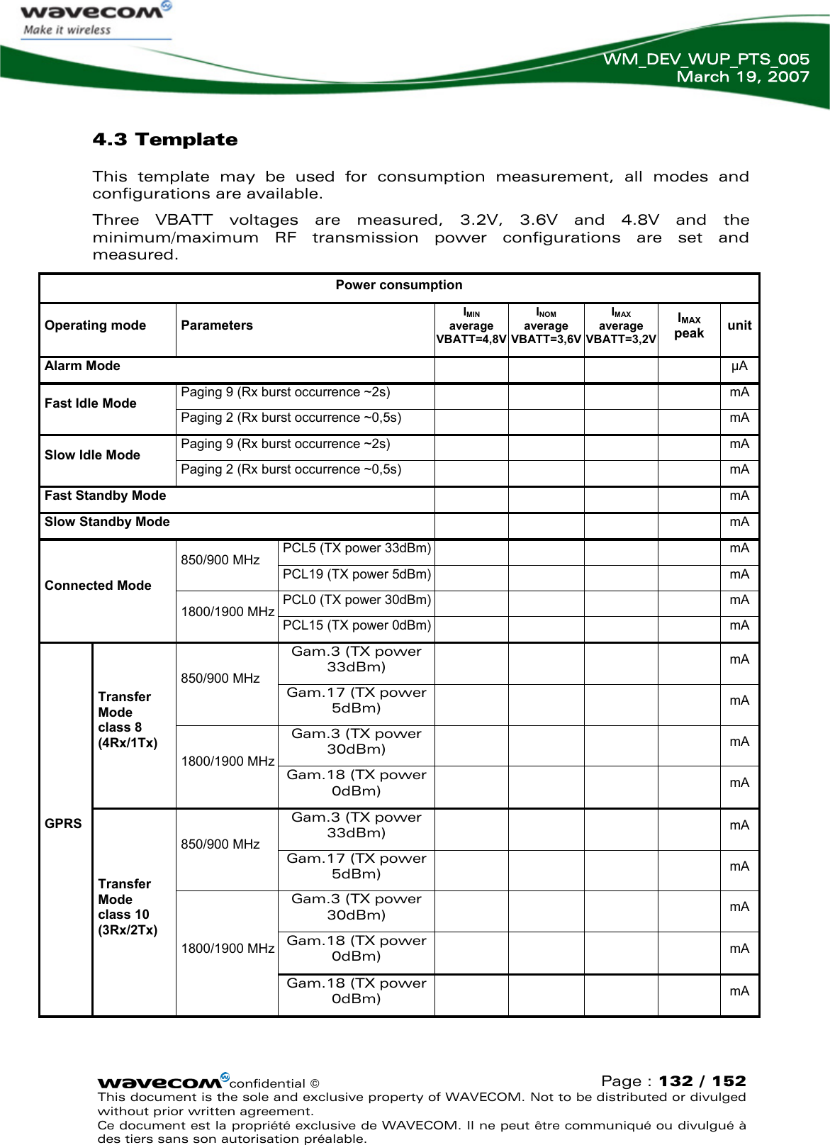
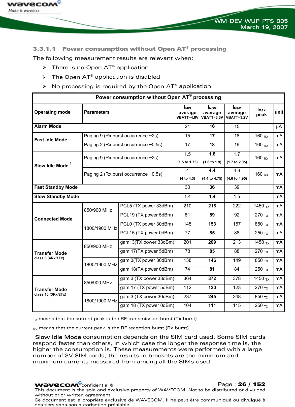
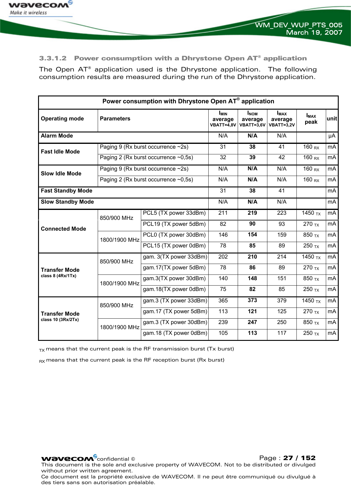
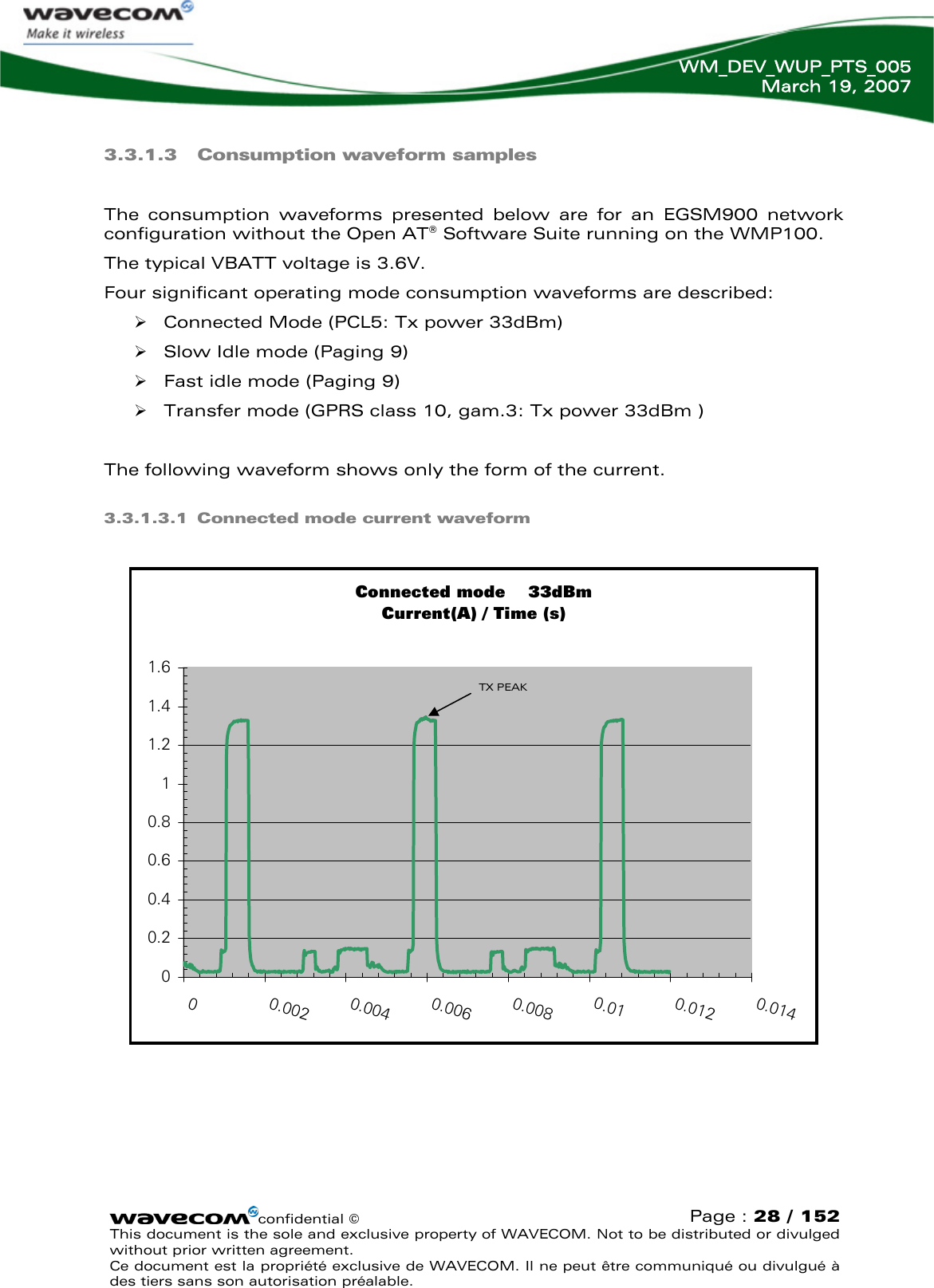
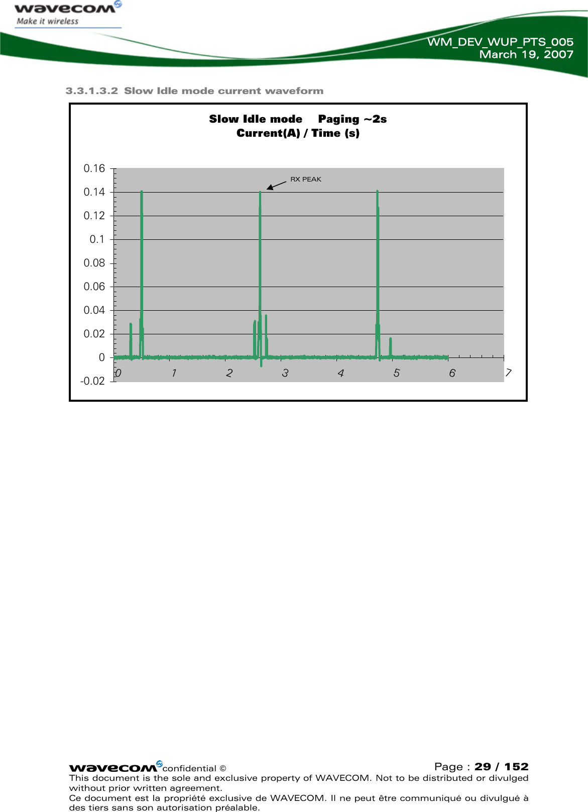
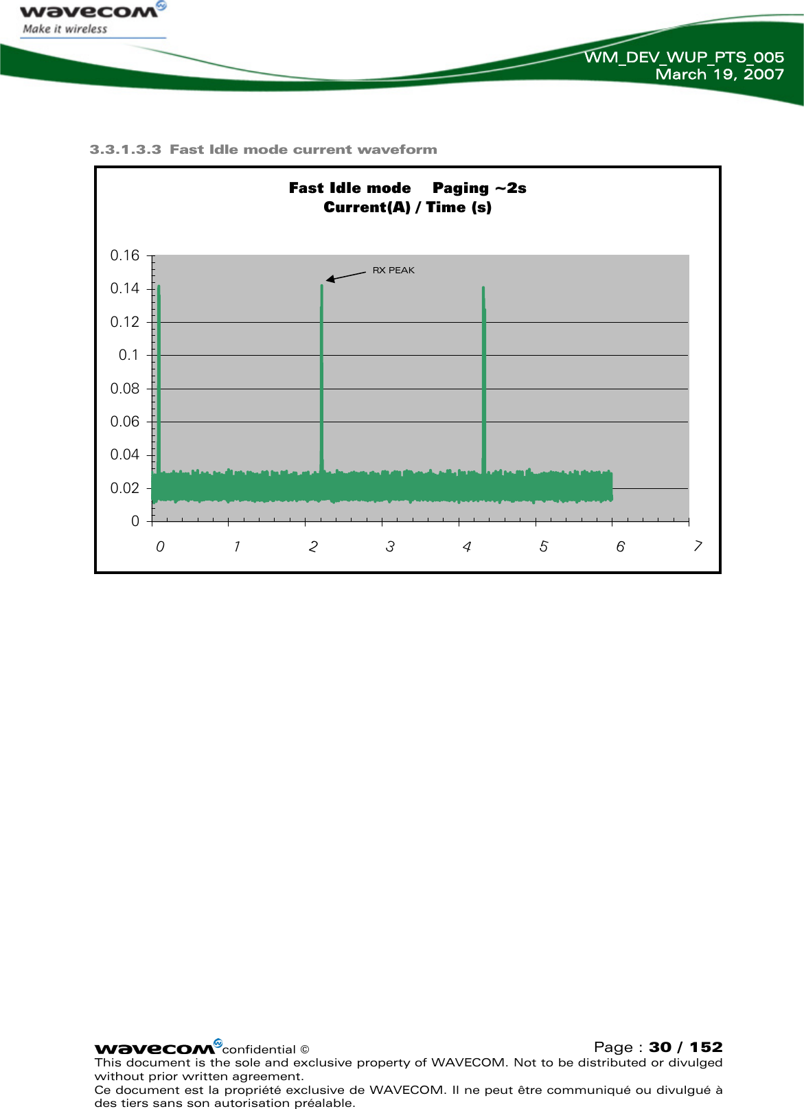
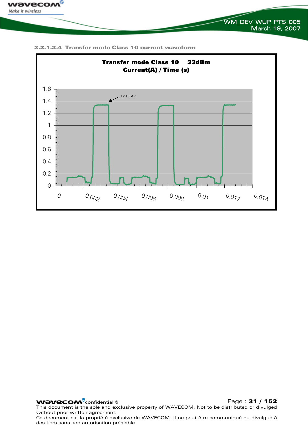
![WM_DEV_WUP_PTS_005 March 19, 2007 3.3 Power consumption Power consumption depends on the configuration used. It is for this reason that the following consumption values are given for each mode, RF band and type of software used (with or without an Open AT® application). Note: All of the following information is given assuming a 50 Ω RF output. The following consumption values were obtained by performing measurements on WMP100 samples at a temperature of 25° C. Three VBATT values are used to measure the consumption, VBATTMIN (3.2V), VBATTMAX (4.8V) and VBATTTYP (3.6V). The average current is given for the three VBATT values and the peak current given is the maximum current peak measured with the three VBATT voltages. For a more detailed description of the operating modes, (refer to the document [3] AT Command Interface Guide for Open AT® Firmware v6.5). For more information about the consumption measurement procedure, refer to § 4. All following consumption measurement values have to be confirmed. confidential © Page : 25 / 152 This document is the sole and exclusive property of WAVECOM. Not to be distributed or divulged without prior written agreement. Ce document est la propriété exclusive de WAVECOM. Il ne peut être communiqué ou divulgué à des tiers sans son autorisation préalable.](https://usermanual.wiki/Sierra-Wireless/WMP100.User-Manual/User-Guide-778441-Page-26.png)
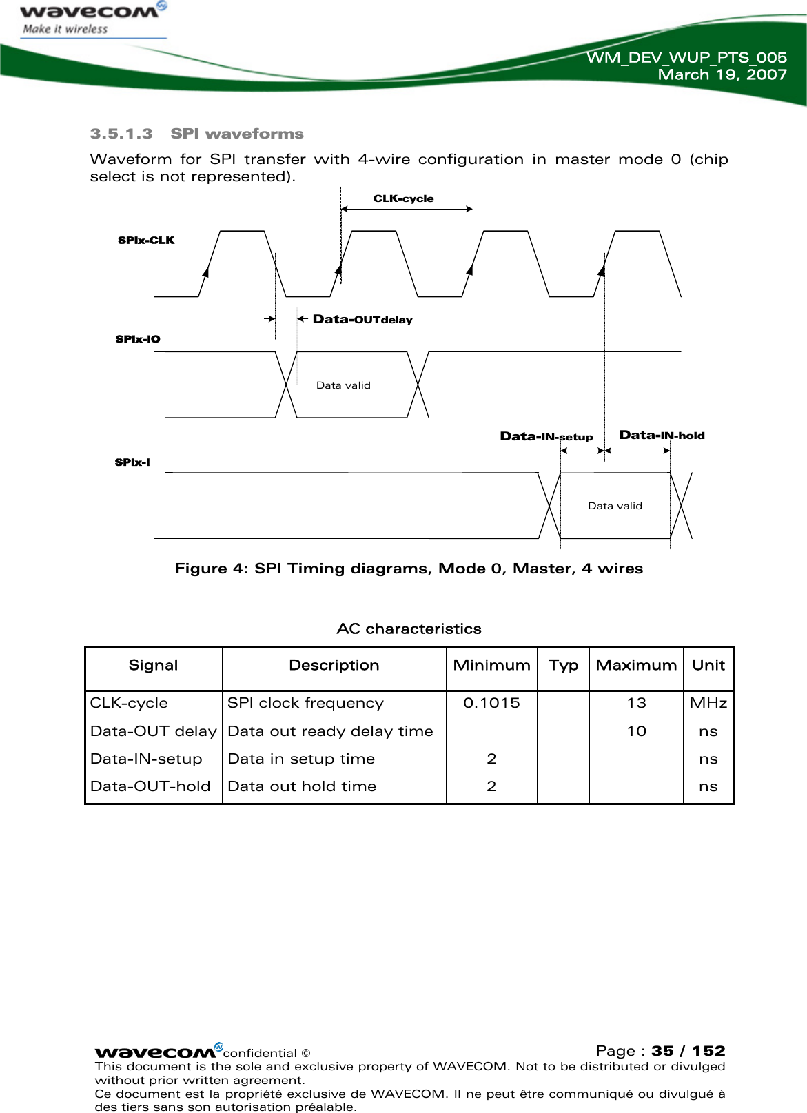
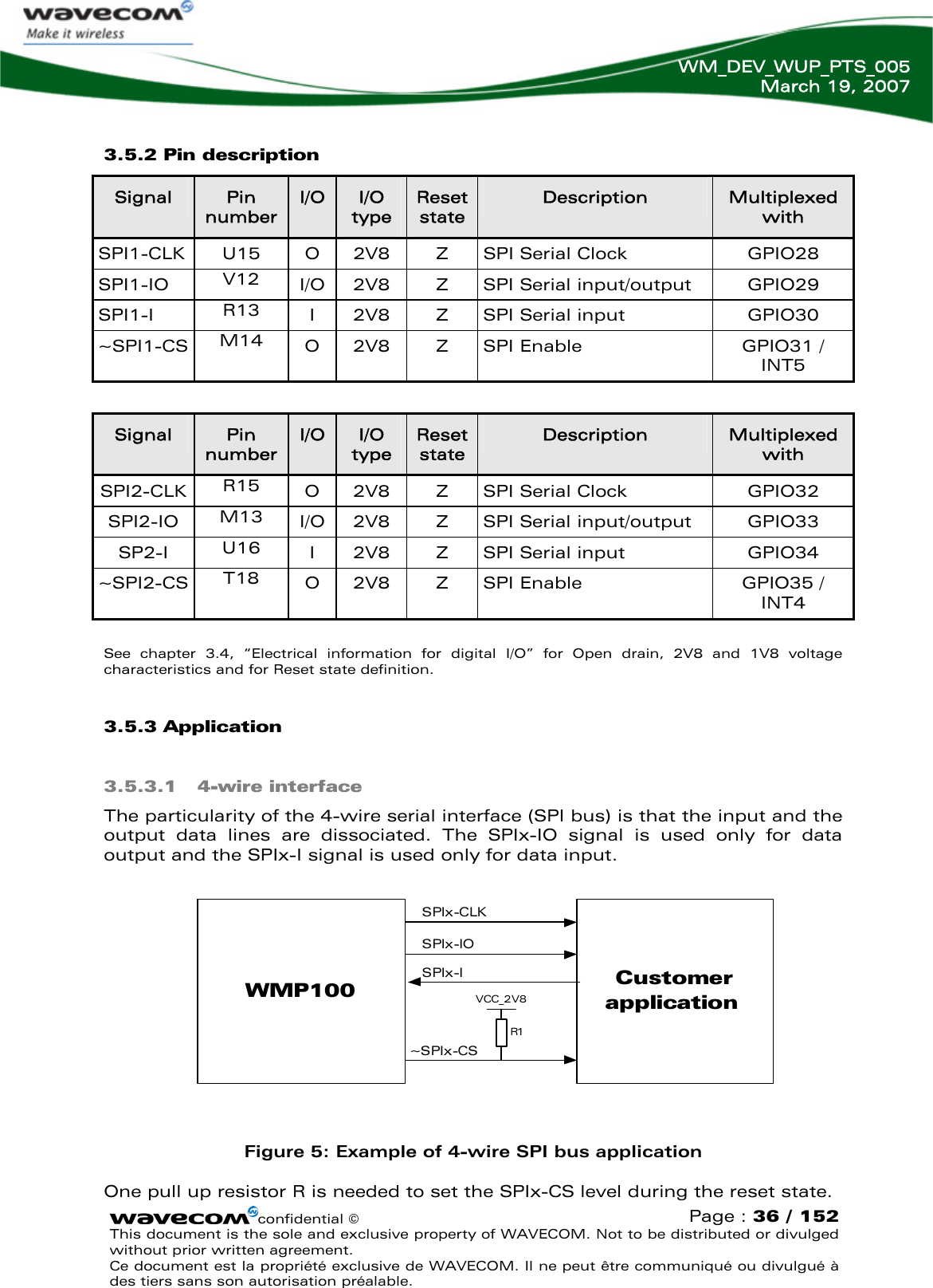
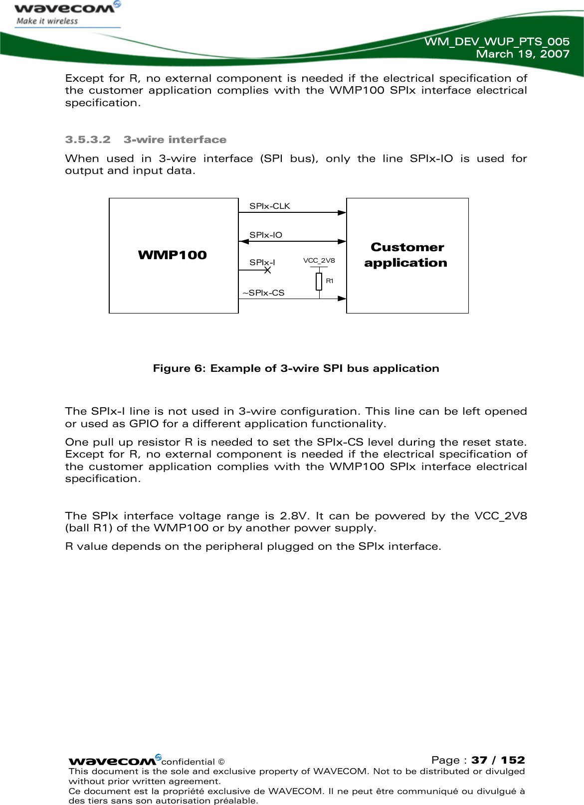
![WM_DEV_WUP_PTS_005 March 19, 2007 confidential © Page : 34 / 152 This document is the sole and exclusive property of WAVECOM. Not to be distributed or divulged without prior written agreement. Ce document est la propriété exclusive de WAVECOM. Il ne peut être communiqué ou divulgué à des tiers sans son autorisation préalable. 3.5 SPI Bus The WMP100 provides two SPI bus (i.e. for LCD, memories…). 3.5.1 Features • a CLK signal • an I/O signal • an I signal • a CS signal complying with standard SPI bus. 3.5.1.1 Characteristics • Master mode operation • The Hardware CS is usable only for word handling mode. In normal mode the CS can be any GPIO. • The SPI speed is from 102 Kbit/s up to 13 Mbit/s in master mode operation • 3 or 4-wire interface • SPI-mode configuration: 0 to 3 (for more details, refer to document [3] AT Command Interface Guide for Open AT® Firmware v6.5). • 1 to 16 bits data length 3.5.1.2 SPI configuration Operation Maximum Speed SPI-Mode Duplex 3-wire type 4-wire type Master 13 Mb/s 0,1,2,3 Half SPIx-CLK; SPIx-IO; ~SPIx-CS SPIx-CLK; SPIx-IO; SPIx-I; ~SPIx-CS For the 4-wire configuration, SPIx-I/O is used as output only, SPIx-I is used as input only. For the 3-wire configuration, SPIx-I/O is used as input and output.](https://usermanual.wiki/Sierra-Wireless/WMP100.User-Manual/User-Guide-778441-Page-35.png)
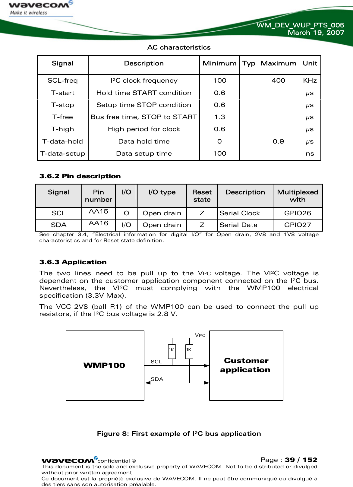
![WM_DEV_WUP_PTS_005 March 19, 2007 3.6 I2C bus 3.6.1 Features The I2C interface includes a clock signal (SCL) and a data signal (SDA) complying with a 100Kbit/s-standard interface (standard mode: s-mode). 3.6.1.1 Characteristics The I²C bus is always master. The maximum speed transfer range is 400Kbit/s (Fast mode: f-mode). For more information on the bus, see document [4] “I²C Bus Specification”, Version 2.0, Philips Semiconductor 1998. 3.6.1.2 I²C waveforms I²C bus waveform in master mode configuration: confidential © Page : 38 / 152 This document is the sole and exclusive property of WAVECOM. Not to be distributed or divulged without prior written agreement. Ce document est la propriété exclusive de WAVECOM. Il ne peut être communiqué ou divulgué à des tiers sans son autorisation préalable. Data validSCL-freqT-freeT-startT-highT-data-setupT-data-holdT-stopSCLSDAData valid Figure 7: I²C Timing diagrams, Master](https://usermanual.wiki/Sierra-Wireless/WMP100.User-Manual/User-Guide-778441-Page-39.png)
![WM_DEV_WUP_PTS_005 March 19, 2007 For the use case with 5-wire serial interface • Signal: CT103/TXD1*, CT104/RXD1*, ~CT105/RTS1*, ~CT106/CTS1* • The signal ~CT108-2/DTR1* must be managed following the V24 protocol signalling if we want to use the slow idle mode • The other signals and their multiplexed are not available • Please refer to the document [3] AT Command Interface Guide for Open AT® Firmware v6.5 for more information. For the use case with 4-wire serial interface • CT103/TXD1*, CT104/RXD1*, ~CT105/RTS1*, ~CT106/CTS1* • The signal ~CT108-2/DTR1* must be configured at the low level • The other signals and their multiplexed are not available • Please refer to the document [3] AT Command Interface Guide for Open AT® Firmware v6.5 for more information. For the use case with 2-wire serial interface • This case is possible for connected external chip but not recommended (and forbidden for AT command or modem use) • The external chip must be a flow control • CT103/TXD1*, CT104/RXD1* • The signal ~CT108-2/DTR1* must be configured at the low level • The signals ~CT105/RTS1*, ~CT106/CTS1* are not used, please configure the AT command (AT+IFC=0,0 see document [3] AT Command Interface Guide for Open AT® Firmware v6.5). • The signal ~CT105/RTS1* must be configured at the low level • The other signals and their multiplexed are not available • Please refer to the document [3] AT Command Interface Guide for Open AT® Firmware v6.5 for more information. confidential © Page : 44 / 152 This document is the sole and exclusive property of WAVECOM. Not to be distributed or divulged without prior written agreement. Ce document est la propriété exclusive de WAVECOM. Il ne peut être communiqué ou divulgué à des tiers sans son autorisation préalable.](https://usermanual.wiki/Sierra-Wireless/WMP100.User-Manual/User-Guide-778441-Page-45.png)
![WM_DEV_WUP_PTS_005 March 19, 2007 Customerapplication( DTE )WMP100( DCE )GND~RESET~CT107-DSR1 / GPIO40~CT109-DCD1 / GPIO43~CT108-2-DTR1 / GPIO41~CT125-RI1 / GPIO42AB16M16AA18V6T12GNDDCDDTRRIGNDDSRON / ~OFFU5CT103-TXD1 / GPIO36CT104-RXD1 / GPIO37~CT105-RTS1 / GPIO38~CT106-CTS1 / GOPI39N15Y18T13R17RxRTSCTSTx2x 15K2.8Volt Figure 14: Example of full modem V24/CMOS serial link implementation for UART1 It is recommended to add a 15K-ohm pull-up resistor on ~CT125-RI1 and ~CT109-DCD1 to set high level during reset state. The UART1 interface is 2.8 Volt type, but is 3 Volt tolerant. The WMP100 UART1 is designed to operate using all the serial interface signals. In particular, it is mandatory to use RTS and CTS for hardware flow control in order to avoid data corruption during transmission. Warning: If you want to activate Power Down mode (Wavecom 32K mode) in your Open AT® application, you need to wire the DTR ball to a GPIO. Please refer to the document [3] AT Command Interface Guide for Open AT® Firmware v6.5 (see the “Appendixes”) for more information on Wavecom 32K mode activation using the Open AT® Software Suite. confidential © Page : 49 / 152 This document is the sole and exclusive property of WAVECOM. Not to be distributed or divulged without prior written agreement. Ce document est la propriété exclusive de WAVECOM. Il ne peut être communiqué ou divulgué à des tiers sans son autorisation préalable.](https://usermanual.wiki/Sierra-Wireless/WMP100.User-Manual/User-Guide-778441-Page-50.png)
![WM_DEV_WUP_PTS_005 March 19, 2007 3.9 Auxiliary serial link (UART2) An auxiliary serial interface (UART2) is available on WMP100. This interface may be used to connect a Bluetooth or a GPS chip controlled by an Open AT® Plug-in. 3.9.1 Features Maximum baud rate of the UART2 is 460 Kbit/s. The signals are the follows: • TX data (CT103/TX) • RX data (CT104/RX) • Request To Send (~CT105/RTS) • Clear To Send (~CT106/CTS) The WMP100 is designed to operate using all the serial interface signals. In particular, it is mandatory to use RTS and CTS for hardware flow control in order to avoid data corruption during transmission. For the use case with 2-wire serial interface • This case is possible for connected external chip but not recommended (and forbidden for AT command or modem use) • The external chip must be a flow control • CT103/TXD2*, CT104/RXD2* • The signals ~CT105/RTS2*, ~CT106/CTS2* are not used, please configure the AT command (AT+IFC=0,0. Please refer to the document [3] AT Command Interface Guide for Open AT® Firmware v6.5. • The signal ~CT105/RTS2* must be configured at the low level • The other signal and their multiplexed are not available • Please refer to the document [3] AT Command Interface Guide for Open AT® Firmware v6.5 (see the “Appendixes”). confidential © Page : 50 / 152 This document is the sole and exclusive property of WAVECOM. Not to be distributed or divulged without prior written agreement. Ce document est la propriété exclusive de WAVECOM. Il ne peut être communiqué ou divulgué à des tiers sans son autorisation préalable.](https://usermanual.wiki/Sierra-Wireless/WMP100.User-Manual/User-Guide-778441-Page-51.png)
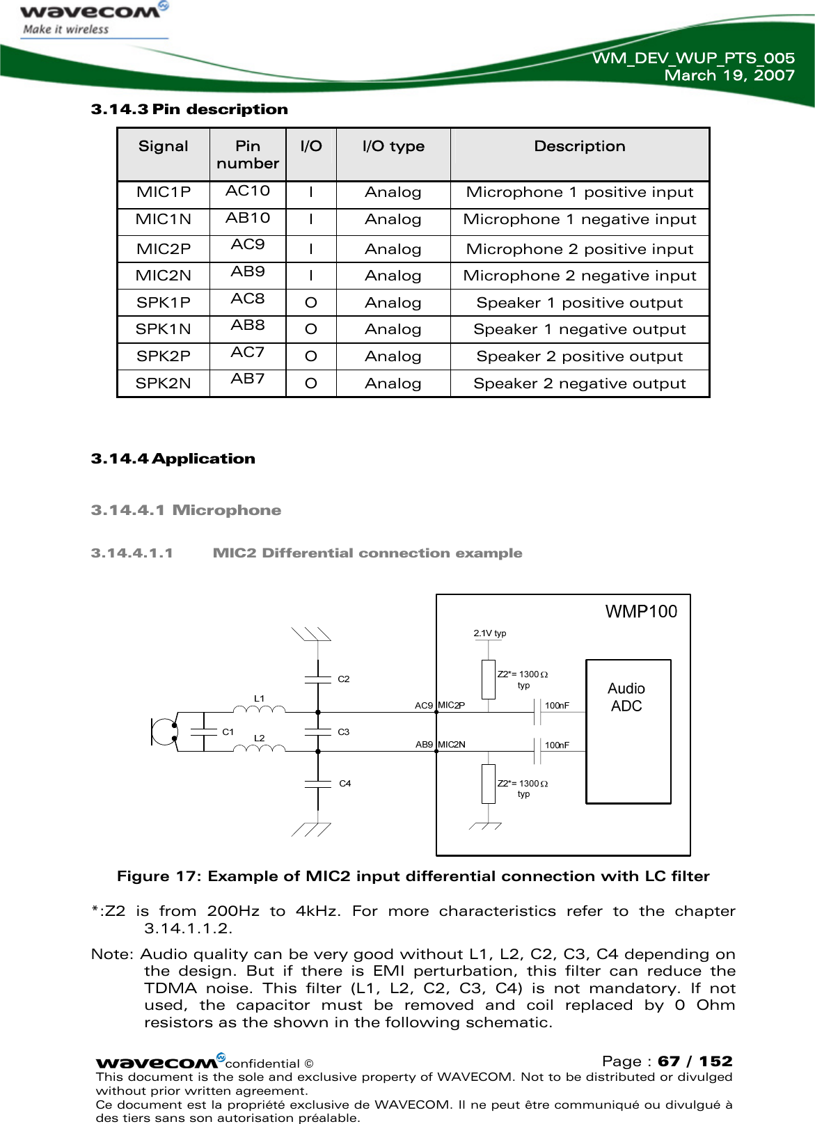
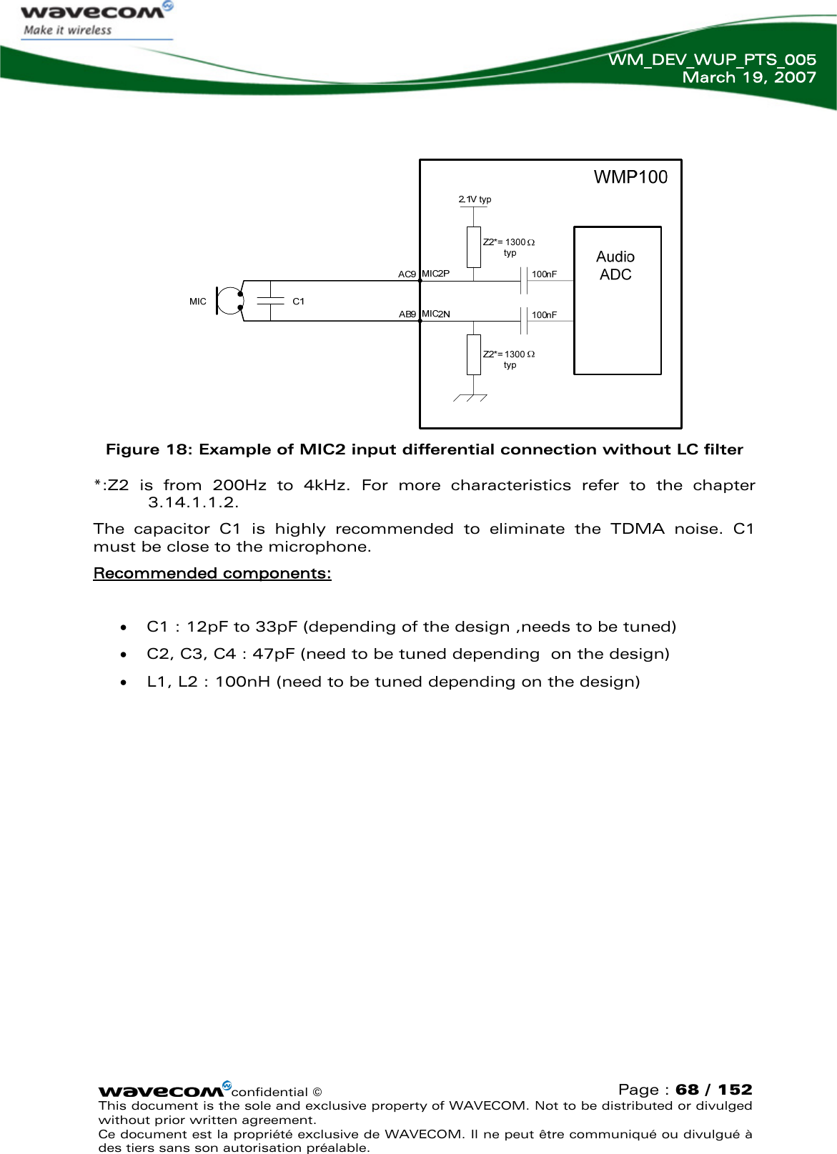
![WM_DEV_WUP_PTS_005 March 19, 2007 Parameters Min Typ Max Unit DC Characteristics N/A V AC Characteristics 200 Hz<F<4 kHz Z1 70 120 160 KΩ AT+VGT*=2 13.8 mVrms AT+VGT*=1 77.5 confidential © Page : 62 / 152 This document is the sole and exclusive property of WAVECOM. Not to be distributed or divulged without prior written agreement. Ce document est la propriété exclusive de WAVECOM. Il ne peut être communiqué ou divulgué à des tiers sans son autorisation préalable. Maximum working voltage ( MIC1P-MIC1N) AT+VGT*=0 346 Positive +7.35 V Maximum rating voltage (MIC1P or MIC1N) Negative -0.9 • *The input voltage depends of the input micro gain set by AT command. Please refer to the document [3] AT Command Interface Guide for Open AT® Firmware v6.5. 3.14.1.1.2 MIC2 Microphone Inputs By default, the MIC2 inputs are differential ones, but it can be configured in single ended. They already include the convenient biasing for an electret microphone. The electret microphone can be directly connected on those inputs, thus allowing easy connection to a handset. AC coupling is already embedded in the Wireless Microprocessor®. Equivalent circuits of MIC2 DC equivalent circuit AC equivalent circuit Electrical Characteristics of MIC2 MIC2P MIC2N Z2 Z2 GND MIC2+ MIC2P MIC2N RRGND](https://usermanual.wiki/Sierra-Wireless/WMP100.User-Manual/User-Guide-778441-Page-63.png)
![WM_DEV_WUP_PTS_005 March 19, 2007 Parameters Min Typ Max Unit MIC2+ 2 2.1 2.2 V Output current 0.5 1.5 confidential © Page : 63 / 152 This document is the sole and exclusive property of WAVECOM. Not to be distributed or divulged without prior written agreement. Ce document est la propriété exclusive de WAVECOM. Il ne peut être communiqué ou divulgué à des tiers sans son autorisation préalable. mA Internal biasing DC Characteristics R2 1650 1900 2150 Ω Z2 MIC2P (MIC2N=Open) Z2 MIC2N (MIC2P=Open) 1.1 1.3 1.6 Z2 MIC2P (MIC2N=GND) Z2 MIC2N (MIC2P=GND) 0.9 1.1 1.4 AC Characteristics 200 Hz<F<4 kHz Impedance between MIC2P and MIC2N 1.3 1.6 2 KΩ AT+VGT*=2 13.8 AT+VGT*=1 77.5 Maximum working voltage ( MIC2P-MIC2N) AT+VGT*=0 346 mVrms Positive +7.35** Maximum rating voltage (MIC2P or MIC2N) Negative -0.9 V • *The input voltage depends of the input micro gain set by AT command. Please refer to the document [3] AT Command Interface Guide for Open AT® Firmware v6.5 • **Because MIC2P is internally biased, it is necessary to use a coupling capacitor to connect an audio signal provided by an active generator. Only a passive microphone can be directly connected to the MIC2P and MIC2N inputs.](https://usermanual.wiki/Sierra-Wireless/WMP100.User-Manual/User-Guide-778441-Page-64.png)
![WM_DEV_WUP_PTS_005 March 19, 2007 Parameters Min Typ Max Unit Biasing voltage - 1.30 V RL=16Ω: AT+VGR=6; single-ended - 1.7 - Vpp Output swing voltage RL=32Ω; AT+VGR=6; single-ended - 1.9 2.75 Vpp RL Load resistance 14.5 32 - Ω RL=16Ω - 40 85 mA IOUT Output current; single-ended; peak value RL=32Ω - 22 - mA RL=16Ω; AT+VGR*=6 - 25 mW POUT RL=32Ω; AT+VGR*=6 - 16 27 mW RPD Output pull-down resistance at power-down 28 40 52 KΩ *The output voltage depends of the output speaker gain set by AT command. Please refer to the document [3] AT Command Interface Guide for Open AT® Firmware v6.5. confidential © Page : 65 / 152 This document is the sole and exclusive property of WAVECOM. Not to be distributed or divulged without prior written agreement. Ce document est la propriété exclusive de WAVECOM. Il ne peut être communiqué ou divulgué à des tiers sans son autorisation préalable.](https://usermanual.wiki/Sierra-Wireless/WMP100.User-Manual/User-Guide-778441-Page-66.png)
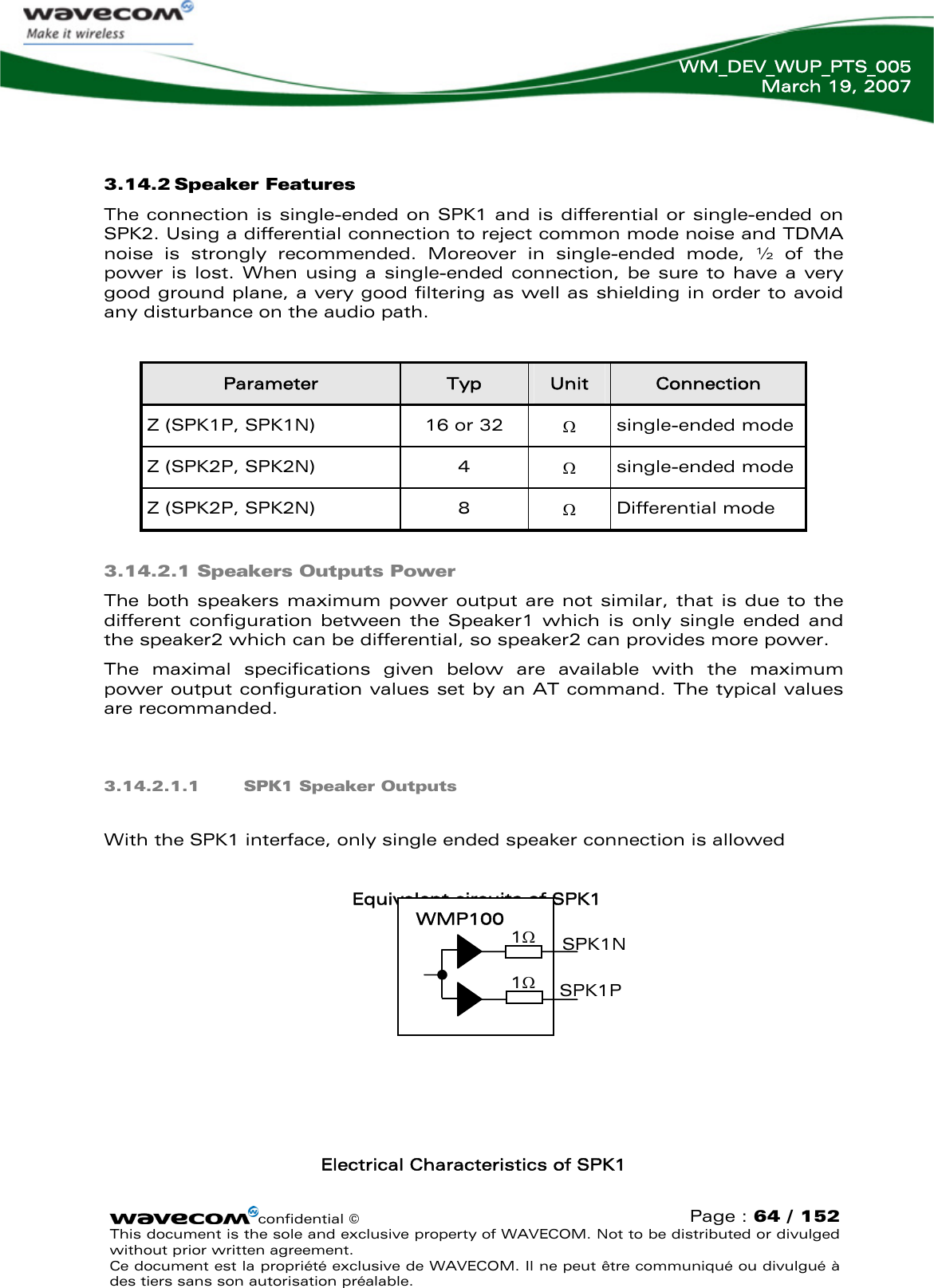
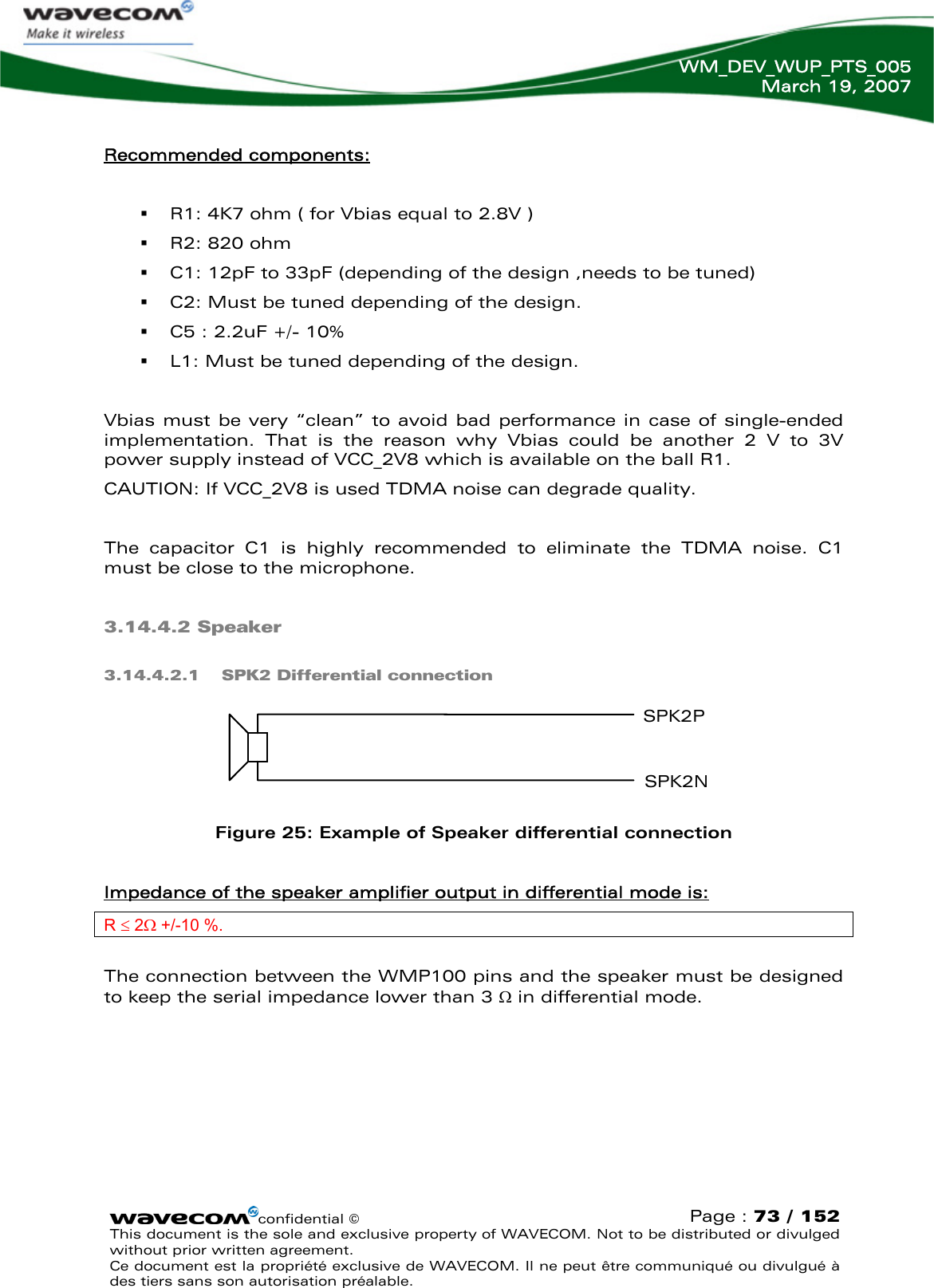
![WM_DEV_WUP_PTS_005 March 19, 2007 confidential © Page : 66 / 152 This document is the sole and exclusive property of WAVECOM. Not to be distributed or divulged without prior written agreement. Ce document est la propriété exclusive de WAVECOM. Il ne peut être communiqué ou divulgué à des tiers sans son autorisation préalable. 3.14.2.1.2 SPK2 Speaker Outputs The SPK2 interface allows differential and single ended speaker connection Equivalent circuits of SPK2 Electrical Characteristics of SPK2 Parameters Min Typ Max Unit Biasing voltage SPK2P and SPK2N 1.30 V RL=8Ω: AT+VGR=6*; single ended - - 2 Vpp RL=8Ω: AT+VGR=6*; differential - - 4 Vpp RL=32Ω: AT+VGR=6*; single ended - - 2.5 Vpp Output swing voltage RL=32Ω: AT+VGR=6*; differential - - 5 Vpp RL Load resistance 6 8 - Ω IOUT Output current; peak value; RL=8Ω - - 180 mA POUT RL=8Ω; AT+VGR=6*; - - 250 mW RPD Output pull-down resistance at power-down 28 40 52 KΩ VPD Output DC voltage at power-down - - 100 mV *The output voltage depends of the output speaker gain set by AT command. Please refer to the document [3] AT Command Interface Guide for Open AT® Firmware v6.5. If a singled ended solution is used with the speaker2 output, only one of the both SPK2 has to be chosen. The result is a maximal output power divided by 2. 1Ω 1Ω SPKWMP100 + SPK2N SPK2P](https://usermanual.wiki/Sierra-Wireless/WMP100.User-Manual/User-Guide-778441-Page-67.png)
![WM_DEV_WUP_PTS_005 March 19, 2007 The recommended way to de-assert the ON/~OFF signal is to use either an AT command or WIND indicators: the application has to detect the end of the power-up initialization and de-assert ON/~OFF afterwards. • Send an “AT” command and wait for the “OK” answer: once the initialization is complete the AT interface answers « OK » to “AT” message1. • Wait for the “+WIND: 3” message: after initialization, the WMP100/Open AT® Software Suite v1.0, if configured to do so, will return an unsolicited “+WIND: 3” message. The generation of this message is enabled or disabled via an AT command. Note: • Please refer to the document [3] AT Command Interface Guide for Open AT® Firmware v6.5 for more information on these commands. Proceeding thus – by software detection - will always prevent the application from de-asserting the ON/~OFF signal too early. If WIND indicators are disabled or AT commands unavailable or not used, it is still possible to de-assert ON/~OFF after a delay long enough (Ton/off-hold) to ensure that the firmware has already completed its power-up initialization. The table below gives the minimum values of Ton/off-hold: Ton/off-hold minimum values Ton/off-hold Open AT® Firmware Safe evaluations of the firmware power-up time 6.65 & above 8 s The above figure take the worst cases into account: power-loss recovery operations, slow flash memory operations in high temperature conditions, and so on. But they are safe because they are large enough to ensure that ON/~OFF is not de-asserted too early. Additional notes: 1. Typical power-up initialization time figures for best cases conditions (no power-loss recovery, fast and new flash memory…) approximate 3.5 seconds in every firmware version. But releasing ON/~OFF after this delay does not guarantee that the application will actually start-up if for example the power plug has been pulled off during a flash memory operation, like a phone book entry update or an AT&W command… 2. The ON/~OFF signal can be left at a high level until switch OFF. But this is not recommended as it will prevent the AT+CPOF command from performing a clean power-off. (see also <<<NOTE IN POWER OFF CHAPTER>>> for an alternate usage) confidential © Page : 86 / 1521 If the application manages hardware flow control, the AT command can be sent during the initialisation phase. This document is the sole and exclusive property of WAVECOM. Not to be distributed or divulged without prior written agreement. Ce document est la propriété exclusive de WAVECOM. Il ne peut être communiqué ou divulgué à des tiers sans son autorisation préalable.](https://usermanual.wiki/Sierra-Wireless/WMP100.User-Manual/User-Guide-778441-Page-87.png)
![WM_DEV_WUP_PTS_005 March 19, 2007 It’s recommended to add an ESD protection component on the antenna line, in order to increase the final product ESD tolerance. ESD protection Figure 64: RF connector and ESD protection example This ESD protection component can be an 82 nH Multi-Layer HF inductor (0603 case). It must be connected between RF output and ground as short as possible. It’s also possible to use an antenna chip or to choose to design an antenna directly on the same PCB. WARNING: Wavecom strongly recommends working with an antenna manufacturer either to develop an antenna adapted to the application or to adapt an existing solution to the application. Both the mechanical and electrical antenna adaptation is one of the key issues in the design of the GSM terminal. 4 Consumption measurement procedure This chapter describes the consumption measurement procedure used to obtain the Wireless Microprocessor consumption specification WMP100/OASS1.0 consumption specification values are measured for all operating modes available on this product. See the appendix of document [3] AT Command Interface Guide for Open AT® Firmware v6.5. Consumption results are highly dependent on the hardware configuration used during measurement, this chapter describes the hardware configuration settings to be used to obtain optimum consumption measurements. 4.1 Hardware configuration The hardware configuration includes both the measurement equipment and the Wireless Microprocessor with its motherboard. 4.1.1 Equipment Four devices are used to perform consumption measurement. ¾ A communication tester ¾ A current measuring power supply confidential © Page : 127 / 152 This document is the sole and exclusive property of WAVECOM. Not to be distributed or divulged without prior written agreement. Ce document est la propriété exclusive de WAVECOM. Il ne peut être communiqué ou divulgué à des tiers sans son autorisation préalable.](https://usermanual.wiki/Sierra-Wireless/WMP100.User-Manual/User-Guide-778441-Page-128.png)
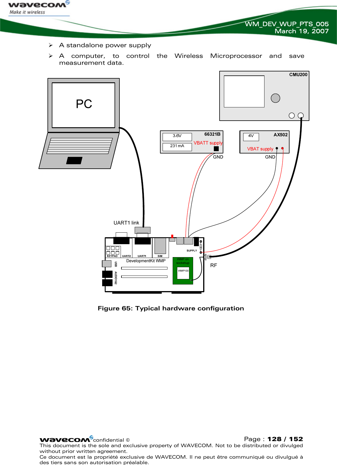
![WM_DEV_WUP_PTS_005 March 19, 2007 confidential © Page : 129 / 152 This document is the sole and exclusive property of WAVECOM. Not to be distributed or divulged without prior written agreement. Ce document est la propriété exclusive de WAVECOM. Il ne peut être communiqué ou divulgué à des tiers sans son autorisation préalable. The communication tester is a CMU 200 from Rhode & Schwartz. This tester offers all GSM/GPRS network configurations required and allows a wide range of network configurations to be set. The AX502 standalone power supply is used to supply all motherboard components except the Wireless Microprocessor. The goal is to separate motherboard consumption from Wireless Microprocessor consumption -which is measured by the other power supply, the 66321B “current measuring power supply”. The “current measuring power supply” is also connected and controlled by the computer (GPIB control not shown in the previous figure). A SIM must be inserted in the Development Kit Wireless Microprocessor during all consumption measurements. Equipment reference list: Device Manufacturer Reference Communication Tester Rhode & Schwartz CMU 200 Quad Band GSM/DCS/GPRS Current measuring power supply Agilent 66321B Used for VBATT (for WMP alone) Stand alone power supply Metrix AX502 Used for VBAT (for boards peripherals) 4.1.2 Wireless Microprocessor motherboard The Wireless Microprocessor board used is the Development Kit Wireless Microprocessor V2. This board can be used to perform consumption measurement with several settings. For a description of the settings, see document [2] WMP100 Development Kit User Guide. The Wireless Microprocessor is only powered by VBATT. The Development Kit board is powered by the standalone power supply at VBAT. It is for this reason that the link between VBATT and VBAT (J605) must be opened (by removing the solder at the top of board in the SUPPLY area). ¾ VBATT powered by the current measuring power supply (66321B). ¾ VBAT powered by the standalone power supply (AX502). The R600, resistor, and D603,D604 diodes (around the BAT-TEMP connector) must be removed. The UART2 link is not used, therefore J201, J202, J203, J204 must be opened (by removing the solder). The “FLASH-LED” must be not used, so J602 must be opened (by removing the solder).](https://usermanual.wiki/Sierra-Wireless/WMP100.User-Manual/User-Guide-778441-Page-130.png)
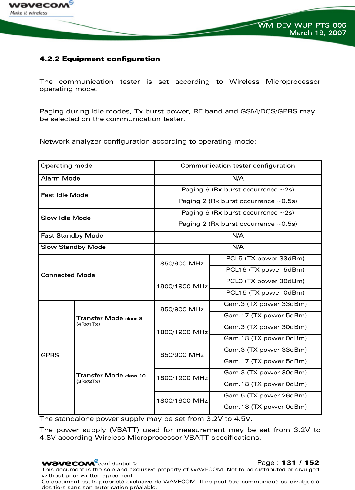
![WM_DEV_WUP_PTS_005 March 19, 2007 The USB link is not used, therefore J301, J302, J303, J304, J305 must be opened (by removing the solder). Around “CONFIG” area, the switch BOOT must be to OFF position. The goal of the settings is to eliminate all bias current from VBATT and to supply the entire board (except the Wireless Microprocessor) via VBAT only. The standalone power supply may be set to 4 Volts. 4.1.3 SIM cards used Consumption measurement may be performed with 3-Volt or 1.8-Volt SIM cards. However, all specified consumption values are for a 3-Volt SIM card. CAUTION: The SIM card is supplied by the Wireless Microprocessor, consumption measurement results may vary depending of the SIM card used. 4.2 Software configurations Software configuration for the equipment and Wireless Microprocessor settings. 4.2.1 Wireless Microprocessor configuration Wireless Microprocessor software configuration is simply performed by selecting the operating mode to be used to perform the measurement. A description of the operating modes and the procedure used to change operating mode are given in the appendix of document [3] AT Command Interface Guide for Open AT® Firmware v6.5. An overview of the WMP100/OASS1.0 operating modes is given below: ¾ Alarm Mode ¾ Fast Idle Mode ¾ Slow Idle Mode ¾ Fast Standby Mode ¾ Slow Standby Mode ¾ Connected Mode ¾ Transfer Mode class 8 (4Rx/1Tx) (in GPRS mode) ¾ Transfer Mode class 10 (3Rx/2Tx) (in GPRS mode) confidential © Page : 130 / 152 This document is the sole and exclusive property of WAVECOM. Not to be distributed or divulged without prior written agreement. Ce document est la propriété exclusive de WAVECOM. Il ne peut être communiqué ou divulgué à des tiers sans son autorisation préalable.](https://usermanual.wiki/Sierra-Wireless/WMP100.User-Manual/User-Guide-778441-Page-131.png)