Sierra Wireless WMP100 GSM Module User Manual User Guide
Sierra Wireless Inc. GSM Module User Guide
Contents
- 1. User Manual
- 2. User Guide
User Guide

WA_DEV_WMPR_PTS_001
001
September 20, 2010
AirPrime WMP Series
User Guide (DRAFT)

WA_DEV_WMPR_PTS_001 Rev 001 September 20, 2010 2
User Guide
Important Notice
Due to the nature of wireless communications, transmission and reception of data can never be
guaranteed. Data may be delayed, corrupted (i.e., have errors) or be totally lost. Although significant
delays or losses of data are rare when wireless devices such as the Sierra Wireless modem are used
in a normal manner with a well-constructed network, the Sierra Wireless modem should not be used
in situations where failure to transmit or receive data could result in damage of any kind to the user or
any other party, including but not limited to personal injury, death, or loss of property. Sierra Wireless
accepts no responsibility for damages of any kind resulting from delays or errors in data transmitted or
received using the Sierra Wireless modem, or for failure of the Sierra Wireless modem to transmit or
receive such data.
Safety and Hazards
Do not operate the Sierra Wireless modem in areas where blasting is in progress, where explosive
atmospheres may be present, near medical equipment, near life support equipment, or any equipment
which may be susceptible to any form of radio interference. In such areas, the Sierra Wireless modem
MUST BE POWERED OFF. The Sierra Wireless modem can transmit signals that could interfere with
this equipment. Do not operate the Sierra Wireless modem in any aircraft, whether the aircraft is on
the ground or in flight. In aircraft, the Sierra Wireless modem MUST BE POWERED OFF. When
operating, the Sierra Wireless modem can transmit signals that could interfere with various onboard
systems.
Note: Some airlines may permit the use of cellular phones while the aircraft is on the ground and the door
is open. Sierra Wireless modems may be used at this time.
The driver or operator of any vehicle should not operate the Sierra Wireless modem while in control of
a vehicle. Doing so will detract from the driver or operator’s control and operation of that vehicle. In
some states and provinces, operating such communications devices while in control of a vehicle is an
offence.
Limitations of Liability
This manual is provided “as is”. Sierra Wireless makes no warranties of any kind, either expressed or
implied, including any implied warranties of merchantability, fitness for a particular purpose, or
noninfringement. The recipient of the manual shall endorse all risks arising from its use.
The information in this manual is subject to change without notice and does not represent a
commitment on the part of Sierra Wireless. SIERRA WIRELESS AND ITS AFFILIATES
SPECIFICALLY DISCLAIM LIABILITY FOR ANY AND ALL DIRECT, INDIRECT, SPECIAL,
GENERAL, INCIDENTAL, CONSEQUENTIAL, PUNITIVE OR EXEMPLARY DAMAGES INCLUDING,
BUT NOT LIMITED TO, LOSS OF PROFITS OR REVENUE OR ANTICIPATED PROFITS OR
REVENUE ARISING OUT OF THE USE OR INABILITY TO USE ANY SIERRA WIRELESS
PRODUCT, EVEN IF SIERRA WIRELESS AND/OR ITS AFFILIATES HAS BEEN ADVISED OF THE
POSSIBILITY OF SUCH DAMAGES OR THEY ARE FORESEEABLE OR FOR CLAIMS BY ANY
THIRD PARTY.
Notwithstanding the foregoing, in no event shall Sierra Wireless and/or its affiliates aggregate liability
arising under or in connection with the Sierra Wireless product, regardless of the number of events,
occurrences, or claims giving rise to liability, be in excess of the price paid by the purchaser for the
Sierra Wireless product.

WA_DEV_WMPR_PTS_001 Rev 001 September 20, 2010 3
User Guide
Patents
This product includes technology licensed from QUALCOMM® 3G.
Manufactured or sold by Sierra Wireless Inc. or its Licensees under one or more patents licensed
from InterDigital Group.
Copyright
© 2010 Sierra Wireless. All rights reserved.
Trademarks
AirCard® and Watcher® are registered trademarks of Sierra Wireless. Sierra Wireless™, AirPrime™,
AirLink™, AirVantage™ and the Sierra Wireless logo are trademarks of Sierra Wireless.
, , ®, inSIM®, WAVECOM®, WISMO®, Wireless Microprocessor®,
Wireless CPU®, Open AT® are filed or registered trademarks of Sierra Wireless S.A. in France and/or
in other countries.
Windows® and Windows Vista® are registered trademarks of Microsoft Corporation.
Macintosh and Mac OS are registered trademarks of Apple Inc., registered in the U.S. and other
countries.
QUALCOMM® is a registered trademark of QUALCOMM Incorporated. Used under license.
Other trademarks are the property of the respective owners.
Contact Information
Sales Desk:
Phone:
1-604-232-1488
Hours:
8:00 AM to 5:00 PM Pacific Time
E-mail:
sales@sierrawireless.com
Post:
Sierra Wireless
13811 Wireless Way
Richmond, BC
Canada V6V 3A4
Fax:
1-604-231-1109
Web:
www.sierrawireless.com
Consult our website for up-to-date product descriptions, documentation, application notes, firmware
upgrades, troubleshooting tips, and press releases: www.sierrawireless.com


WA_DEV_WMPR_PTS_001 Rev 001 September 20, 2010 5
Contents
1. INTRODUCTION .................................................................................................. 9
1.1. Physical Dimensions ......................................................................................................... 9
1.2. GSM/GPRS/EDGE-RX Features ...................................................................................... 9
1.3. Interfaces ........................................................................................................................... 9
1.4. Operating System ............................................................................................................ 10
1.5. Connection Interfaces ..................................................................................................... 10
1.6. Environment and Mechanics ........................................................................................... 10
1.6.1. RoHS Directive Compliant ....................................................................................... 10
1.6.2. Disposing of the Product .......................................................................................... 10
2. FUNCTIONAL SPECIFICATIONS ...................................................................... 11
2.1. RF Functionalities ............................................................................................................ 11
2.2. Operating System ............................................................................................................ 11
3. TECHNICAL SPECIFICATIONS ........................................................................ 12
3.1. Power Supply .................................................................................................................. 12
3.2. Mechanical Specifications ............................................................................................... 13
3.3. Physical Characteristics .................................................................................................. 13
3.3.1. Mechanical Drawings for the WMP100 and WMP150 ............................................. 13
4. INTERFACES ..................................................................................................... 18
4.1. Ball Grid Array Pin Description ........................................................................................ 18
4.2. RF Interface ..................................................................................................................... 25
4.2.1. RF Connections ....................................................................................................... 25
4.2.2. Antenna Specifications ............................................................................................. 25
5. CERTIFICATION COMPLIANCE AND RECOMMENDED STANDARDS ......... 26
5.1. Certification Compliance ................................................................................................. 26
5.2. Applicable Standards Listing ........................................................................................... 26
6. REFERENCES ................................................................................................... 28
6.1. Web Site Support ............................................................................................................ 28
6.2. Reference Documents ..................................................................................................... 29
6.2.1. Sierra Wireless Reference Documentation .............................................................. 29
6.2.2. General Reference Documentation ......................................................................... 29
6.3. List of Abbreviations ........................................................................................................ 30
7. SAFETY RECOMMENDATIONS (FOR INFORMATION ONLY) ....................... 33
7.1. RF Safety ......................................................................................................................... 33
7.1.1. General Information ................................................................................................. 33
7.1.2. Exposure to RF Energy ............................................................................................ 33
7.1.3. Efficient Terminal Operation..................................................................................... 33
7.1.4. Antenna Care and Replacement .............................................................................. 33

WA_DEV_WMPR_PTS_001 Rev 001 September 20, 2010 6
User Guide
7.2. General Safety................................................................................................................. 34
7.2.1. Driving ...................................................................................................................... 34
7.2.2. Electronic Devices .................................................................................................... 34
7.2.3. Vehicle Electronic Equipment .................................................................................. 34
7.2.4. Medical Electronic Equipment .................................................................................. 34
7.2.5. Aircraft ...................................................................................................................... 34
7.2.6. Children .................................................................................................................... 35
7.2.7. Blasting Areas .......................................................................................................... 35
7.2.8. Potentially Explosive Atmospheres .......................................................................... 35

WA_DEV_WMPR_PTS_001 Rev 001 September 20, 2010 7
List of Figures
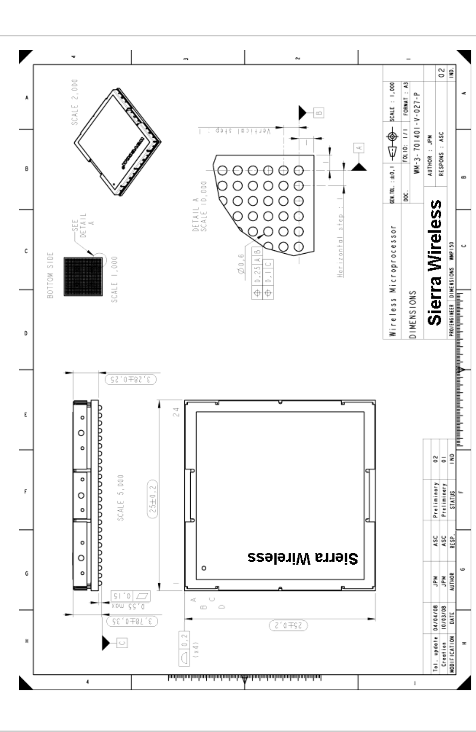
Figure 1. Mechanical Drawing of WMP100 (Bottom View) ............................................................ 14
Figure 2. Mechanical Drawing of WMP100 (Top View) .................................................................. 15
Figure 3. Mechanical Drawing of WMP150 (Bottom View) ............................................................ 16
Figure 4. Mechanical Drawing of WMP150 (Top View) .................................................................. 17

WA_DEV_WMPR_PTS_001 Rev 001 September 20, 2010 8
List of Tables
Table 1. List of RF Frequency Ranges .......................................................................................... 11
Table 2. Input Power Supply Voltage ............................................................................................ 12
Table 3. Maximal Voltage Ripple (Uripp) Versus Frequency ........................................................ 12
Table 4. Mechanical Difference of WMP modules ........................................................................ 13
Table 5. WMP Series Pin Description ........................................................................................... 18
Table 6. Antenna Specifications .................................................................................................... 25
Table 7. Standards Conformity for the WMP Series Embedded Module ...................................... 26
Table 8. Applicable Standards and Requirements for the WMP Series Embedded Module ........ 26

WA_DEV_WMPR_PTS_001 Rev 001 September 20, 2010 9
1. Introduction
The AirPrime WMP50/100/150 and WMP100ESIM/150ESIM Intelligent Embedded Modules are self-
contained E-GSM/GPRS 900/1800 and 850/1900 quad-band embedded modules. In addition, they
are EDGE-Rx capable except for the WMP50.
1.1. Physical Dimensions
Length: 25 mm
Width: 25 mm
Thickness: 3.65 mm for WMP50, WMP100, and WMP100ESIM
3.78 mm for WMP150 and WMP150ESIM
Weight: 4.25 g
1.2. GSM/GPRS/EDGE-RX Features
2 Watts EGSM 900/GSM 850 radio section running under 3.6 Volts
1 Watt GSM1800/1900 radio section running under 3.6 Volts
Hardware GPRS class 10 capable
Hardware EDGE-Rx class 10 capable
1.3. Interfaces
Digital section running under 2.8 Volts and 1.8Volts.
3V/1V8 SIM interface
1.8V Parallel interface for devices (memories, LCD, etc.)
Power supplies
Watchdog
Serial links (UART)
Analogue audio
ADC / DAC
PCM digital audio
Keyboard
USB 2.0 slave
Serial buses (I2C, SPI)
PWM (BUZZER)
GPIOs
SIM (external SIM and optional embedded SIM)

WA_DEV_WMPR_PTS_001 Rev 001 September 20, 2010 10
User Guide
Introduction
1.4. Operating System
Real Time Clock with calendar
Echo Cancellation + noise reduction (quadri codec)
Full GSM or GSM/GPRS/EDGE-Rx Operating System stack
1.5. Connection Interfaces
The WMP series embedded module has a ball grid array pin out that includes:
An RF connection
Baseband signals connection
1.6. Environment and Mechanics
1.6.1. RoHS Directive Compliant
The WMP Series modules are compliant with RoHS Directive 2002/95/EC which sets
limits for the use of certain restricted hazardous substances. This directive states that
“from 1st July 2006, new electrical and electronic equipment put on the market does
not contain lead, mercury, cadmium, hexavalent chromium, polybrominated biphenyls
(PBB) or polybrominated diphenyl ethers (PBDE)”.
1.6.2. Disposing of the Product
This electronic product is subject to the EU Directive 2002/96/EC for Waste Electrical
and Electronic Equipment (WEEE). As such, this product must not be disposed off at
a municipal waste collection point. Please refer to local regulations for directions on
how to dispose of this product in an environmental friendly manner.

WA_DEV_WMPR_PTS_001 Rev 001 September 20, 2010 11
2. Functional Specifications
2.1. RF Functionalities
The Radio Frequency (RF) range complies with the Phase II EGSM 900/DCS 1800 and GSM
850/PCS 1900 recommendation. The frequencies are listed in the table below.
Table 1. List of RF Frequency Ranges
RF Bandwidth
Transmit band (Tx)
Receive band (Rx)
GSM 850
824 to 849 MHz
869 to 894 MHz
E-GSM 900
880 to 915 MHz
925 to 960 MHz
DCS 1800
1710 to 1785 MHz
1805 to 1880 MHz
PCS 1900
1850 to 1910 MHz
1930 to 1990 MHz
The RF part is based on a specific quad band chip including:
a Digital low-IF receiver
a Quad-band LNAs (Low Noise Amplifier)
an Offset PLL (Phase Locked Loop) transmitter
a Frequency synthesizer
a Digitally controlled crystal oscillator (DCXO)
a Tx/Rx FEM (Front-End Module) for quad-band GSM/GPRS/EDGE-Rx
2.2. Operating System
The AirPrime WMP Series embedded module is Sierra Wireless Software Suite compliant. With the
Sierra Wireless Software Suite and the AirPrime WMP Series embedded module, customers can
embed their own applications with the AirPrime WMP and turn the WMP Series embedded module
into a solution for their specific market need.
The operating system allows for the AirPrime WMP Series embedded module to be controlled by AT
commands. However, some interfaces in the AirPrime WMP Series embedded module may still not
be available even with AT command control as these interfaces are dependent on the peripheral
devices connected to the AirPrime WMP Series embedded module.
WA_DEV_WMPR_PTS_001 Rev 001 September 20, 2010 12
3. Technical Specifications
3.1. Power Supply
The following table describes the electrical characteristics of the input power supply voltage that will
guarantee nominal functioning of the AirPrime WMP Series Embedded Modules.
Table 2. Input Power Supply Voltage
VMIN4
VNOM
VMAX
ITYP.
IMAX
Ripple max (Uripp)
VBATT-BB1
3.2
3.6
4.8
0.1 A
0.3 A
100mV3
VBATT-RF1,2
3.2
3.6
4.8
1.4 A
1.5 A
See Table 3 Maximal Voltage
Ripple (Uripp) Versus
Frequency
(1): This value has to be guaranteed during the burst (with 1.5A Peak in GSM or GPRS mode)
(2): Maximum operating Voltage Stationary Wave Ratio (VSWR) 2:1
(3): Take the VBATT-RF ripple max in consideration only if you use the same power supply for VBATT-RF and VBATT-
BB.
(4): The minimum start-up voltage must be 3.3V for WMP100ESIM and WMP150ESIM.
Note: The ESIM version WMP modules require at least 3.3V start-up voltage.
Table 3. Maximal Voltage Ripple (Uripp) Versus Frequency
Freq.
(kHz)
Uripp Max
(mVpp)
Freq.
(kHz)
Uripp Max
(mVpp)
Freq.
(kHz)
Uripp Max
(mVpp)
<100
96
800
27
1500
>60
200
51
900
67
1600
>60
300
37
1000
67
1700
>60
400
15
1100
>60
1800
>60
500
54
1200
>60
>1900
>60
600
21
1300
>60
700
55
1400
>60

WA_DEV_WMPR_PTS_001 Rev 001 September 20, 2010 13
User Guide
Technical Specifications
3.2. Mechanical Specifications
3.3. Physical Characteristics
The WMP modules have a complete self-contained shield. They differ from mechanical dimensions as
described below.
Table 4. Mechanical Difference of WMP modules
Mechanical Difference
WMP50, WMP100, WMP100ESIM
WMP150, WMP150ESIM
Shield Type
Soldered can
Soldered belt and Clip-on cover
Dimension, Thickness
25x25x3.65 mm
25x25x3.78 mm
Weight
4.25 g
4.25 g
3.3.1. Mechanical Drawings for the WMP100 and
WMP150
Refer to the following pages for the mechanical specifications of WMP100 and WMP150 modules.

WA_DEV_WMPR_PTS_001 Rev 001 September 20, 2010 18
4. Interfaces
4.1. Ball Grid Array Pin Description
Pin labeling on the WMP module with Sierra Wireless Software Suite v2.0 is shown below.
Table 5. WMP Series Pin Description
Signal Name
Description
I/O
Voltage Domain
MUX
MUX
MUX
Ball Number
VBATT-RF
Power Supply
I
VBATT
VBATT-RF
_
_
A12, A13, A14, B12,
B13, B14
VBATT-BB
Power Supply
I
VBATT
VBATT-BB
_
_
AC1, AC2, AD1, AD2
RF-OUT
Radio antenna connection
I/O
Analog RF
RF-OUT
_
_
B23
VCC_2V8
Power Supply
O
VCC_2V8
VCC_2V8
_
_
R1
VCC_1V8
Power Supply
O
VCC_1V8
VCC_1V8
_
_
AD5
BAT-RTC
Power Supply
I/O
BAT-RTC
BAT-RTC
_
_
U6
SIM-CLK
SIM clock
O
1V8 / 2V9
SIM-CLK
_
_
Y2
~SIM-RST
SIM reset
O
1V8 / 2V9
~SIM-RST
_
_
Y1
SIM-IO
SIM data
I/O
1V8 / 2V9
SIM-IO
_
_
W1
SIM-VCC
SIM power supply
O
1V8 / 2V9
SIM-VCC
_
_
W2
SIMPRES
SIM presence detection
I/O
VCC_1V8
SIMPRES
INT8
GPIO18
Y3
MIC1P
Microphone input 1 positive
I
Analog
MIC1P
_
_
AC10
MIC1N
Microphone input 1 negative
I
Analog
MIC1N
_
_
AB10
MIC2P
Microphone input 2 positive
I
Analog
MIC2P
_
_
AC9
MIC2N
Microphone input 2 negative
I
Analog
MIC2N
_
_
AB9
SPK1P
Speaker output 1 positive
O
Analog
SPK1P
_
_
AC8
SPK1N
Speaker output 1 negative
O
Analog
SPK1N
_
_
AB8
SPK2P
Speaker output 2 positive
O
Analog
SPK2P
_
_
AC7

WA_DEV_WMPR_PTS_001 Rev 001 September 20, 2010 19
User Guide
Interfaces
Signal Name
Description
I/O
Voltage Domain
MUX
MUX
MUX
Ball Number
SPK2N
Speaker output 2 negative
O
Analog
SPK2N
_
_
AB7
CHG-IN
Charger input voltage
I
Analog
CHG-IN
_
_
V2, V3
CHG-GATE
Charger transistor control output
O
Analog current
CHG-GATE
_
_
V4
ADC1 / BAT-TEMP
Analog to Digital converter 1
I
Analog
ADC1 / BAT-TEMP
_
_
N18
ADC3
Analog to Digital converter 3
I
Analog
ADC3
_
_
M17
ADC2
Analog to Digital converter 2
I
Analog
ADC2
_
_
N17
DAC0
Digital to Analog converter
O
Analog
DAC0
_
_
V14
XIN_32K
Oscillator crystal input
I
Analog
XIN_32K
_
_
AC24
XOUT_32K
Oscillator crystal output
O
Analog
XOUT_32K
_
_
AB24
~RESET
Input Reset signal
I/O
VCC_1V8
~RESET
_
_
V6
~EXT-RESET
Output External reset
O
VCC_1V8
~EXT-RESET
_
_
AB14
ON/~OFF
Power ON
I
VBATT-BB
ON/~OFF
-
-
U5
BOOT
BOOT control
I
VCC_1V8
BOOT
_
_
W18
LED0
WMP100 & WMP150 Status LED
O
Open Drain
VBATT
LED0
_
_
U3
BUZZER0
Buzzer output control
O
Open Drain
VBATT
BUZZER0
_
_
U4
ROW0
Row Scan of keypad
I/O
VCC_1V8
ROW0
GPIO9
_
AC23
ROW1
Row Scan of keypad
I/O
VCC_1V8
ROW1
GPIO10
_
AD22
ROW2
Row Scan of keypad
I/O
VCC_1V8
ROW2
GPIO11
_
AD21
ROW3
Row Scan of keypad
I/O
VCC_1V8
ROW3
GPIO12
_
AC22
ROW4
Row Scan of keypad
I/O
VCC_1V8
ROW4
GPIO13
_
AD23
COL0
Column Scan of keypad
I/O
VCC_1V8
COL0
GPIO4
_
AD19
COL1
Column Scan of keypad
I/O
VCC_1V8
COL1
GPIO5
_
AD20
COL2
Column Scan of keypad
I/O
VCC_1V8
COL2
GPIO6
_
AC20
COL3
Column Scan of keypad
I/O
VCC_1V8
COL3
GPIO7
_
AC19
COL4
Column Scan of keypad
I/O
VCC_1V8
COL4
GPIO8
_
AC21

WA_DEV_WMPR_PTS_001 Rev 001 September 20, 2010 20
User Guide
Interfaces
Signal Name
Description
I/O
Voltage Domain
MUX
MUX
MUX
Ball Number
PCM-SYNC
PCM frame synchronization
O
VCC_1V8
PCM-SYNC
_
_
Y21
PCM-CLK
PCM clock
O
VCC_1V8
PCM-CLK
_
_
W21
PCM-OUT
PCM data output
O
VCC_1V8
PCM-OUT
_
_
W22
PCM-IN
PCM data input
I
VCC_1V8
PCM-IN
_
_
AA22
CT103 / TXD1
Transmit serial data
I/O
VCC_2V8
CT103 / TXD1
GPIO36
_
R17
CT104 / RXD1
Receive serial data
I/O
VCC_2V8
CT104 / RXD1
GPIO37
_
T13
~CT105 / RTS1
Ready To Send
I/O
VCC_2V8
~CT105 / RTS1
GPIO38
_
Y18
~CT106 / CTS1
Clear To Send
I/O
VCC_2V8
~CT106 / CTS1
GPIO39
_
N15
~CT107 / DSR1
Data Set Ready
I/O
VCC_2V8
~CT107 / DSR1
GPIO40
_
T12
~CT108-2 / DTR1
Data Serial Ready
I/O
VCC_2V8
~CT108-2 / DTR1
GPIO41
_
M16
~CT109 / DCD1
Data Carrier Detect
I/O
VCC_2V8
~CT109 / DCD1
GPIO43
_
AB16
~CT125 / RI1
Ring Indicator
I/O
VCC_2V8
~CT125 / RI1
GPIO42
_
AA18
CT103 / TXD2
Transmit serial data
I/O
VCC_1V8
CT103 / TXD2
INT6
GPIO14
T16
CT104 / RXD2
Receive serial data
I/O
VCC_1V8
CT104 / RXD2
GPIO15
_
U17
~CT105 / RTS2
Ready To Send
I/O
VCC_1V8
~CT105 / RTS2
INT7
GPIO17
V13
~CT106 / CTS2
Clear To Send
I/O
VCC_1V8
~CT106 / CTS2
GPIO16
_
W17
SCL1
I²C serial clock
I/O
Open drain
SCL1
GPIO26
_
AA15
SDA1
I²C serial data
I/O
Open Drain
SDA1
GPIO27
_
AA16
SPI1_CLK
SPI serial clock
I/O
VCC_2V8
SPI1-CLK
GPIO28
_
U15
SPI1_IO
SPI serial data input and output
I/O
VCC_2V8
SPI1-IO
GPIO29
_
V12
SPI1-I
SPI serial data input only input
I/O
VCC_2V8
SPI1-I
GPIO30
_
R13
SPI1-LOAD
SPI load
I/O
VCC_2V8
SPI1-LOAD
INT5
GPIO31
M14
SPI2-CLK
SPI serial clock
I/O
VCC_2V8
SPI2-CLK
GPIO32
_
R15
SPI2-IO
SPI serial data input and output
I/O
VCC_2V8
SPI2-IO
GPIO33
_
M13
SPI2-I
SPI serial data input only input
I/O
VCC_2V8
SPI2-I
GPIO34
_
U16
SPI2- LOAD
SPI load
I/O
VCC_2V8
SPI2-LOAD
INT4
GPIO35
T18
INT3
Interruption input
I/O
VCC_2V8
INT3
GPIO46
_
V18

WA_DEV_WMPR_PTS_001 Rev 001 September 20, 2010 21
User Guide
Interfaces
Signal Name
Description
I/O
Voltage Domain
MUX
MUX
MUX
Ball Number
VPAD-USB
USB power supply
I
VPAD-USB
VPAD-USB
-
-
AB19
USB-DP
Universal Serial Bus Data positive
I/O
VPAD-USB
USB-DP
_
_
W19
USB-DM
Universal Serial Bus Data negative
I/O
VPAD-USB
USB-DM
_
_
AA20
USB-CN
Universal Serial Bus Connect
O
VPAD-USB
USB-CN
_
_
Y20
USB-DET
Universal Serial Bus interruption
I
VCC_1V8
USB-DET
_
_
R14
GPIO44
General Purpose Input Output
I/O
VCC_2V8
GPIO44
_
_
AB13
GPIO19
General Purpose Input Output
I/O
VCC_2V8
GPIO19
_
_
AA17
GPIO21
General Purpose Input Output
I/O
VCC_2V8
GPIO21
_
_
AA13
GPIO20
General Purpose Input Output
I/O
VCC_2V8
GPIO20
_
_
Y13
GPIO47
General Purpose Input Output
I/O
VCC_1V8
GPIO47
_
_
Y15
GPIO48
General Purpose Input Output
I/O
VCC_1V8
GPIO48
_
_
Y16
GPIO0
General Purpose Input Output
I/O
VCC_1V8
GPIO0
_
_
W15
GPIO24
General Purpose Input Output
I/O
VCC_2V8
GPIO24
_
_
N16
GPIO22
General Purpose Input Output
I/O
VCC_2V8
GPIO22
_
_
M15
GPIO23
General Purpose Input Output
I/O
VCC_2V8
GPIO23
_
_
V17
INT0
Interruption input
I/O
VCC_1V8
INT0
A26
GPIO3
V16
INT1
Interruption input
I/O
VCC_2V8
INT1
GPIO25
_
Y19
INT2
Interruption input
I/O
VCC_1V8
INT2
GPIO45
_
Y17
A0
Address bus
O
VCC_1V8
A0
_
_
T19
A1
Address bus
O
VCC_1V8
A1
_
_
U18
A2
Address bus
O
VCC_1V8
A2
_
_
U24
A3
Address bus
O
VCC_1V8
A3
_
_
P24
A4
Address bus
O
VCC_1V8
A4
_
_
N24
A5
Address bus
O
VCC_1V8
A5
_
_
M21
A6
Address bus
O
VCC_1V8
A6
_
_
M24
A7
Address bus
O
VCC_1V8
A7
_
_
N23
A8
Address bus
O
VCC_1V8
A8
_
_
R24

WA_DEV_WMPR_PTS_001 Rev 001 September 20, 2010 22
User Guide
Interfaces
Signal Name
Description
I/O
Voltage Domain
MUX
MUX
MUX
Ball Number
A9
Address bus
O
VCC_1V8
A9
_
_
R22
A10
Address bus
O
VCC_1V8
A10
_
_
P22
A11
Address bus
O
VCC_1V8
A11
_
_
T22
A12
Address bus
O
VCC_1V8
A12
_
_
R23
A13
Address bus
O
VCC_1V8
A13
_
_
M22
A14
Address bus
O
VCC_1V8
A14
_
_
P21
A15
Address bus
O
VCC_1V8
A15
_
_
R21
A16
Address bus
O
VCC_1V8
A16
_
_
P23
A17
Address bus
O
VCC_1V8
A17
_
_
T21
A18
Address bus
O
VCC_1V8
A18
_
_
T24
A19
Address bus
O
VCC_1V8
A19
_
_
M23
A20
Address bus
O
VCC_1V8
A20
_
_
N21
A21
Address bus
O
VCC_1V8
A21
_
_
N22
A22
Address bus
O
VCC_1V8
A22
_
_
M20
A23
Address bus
O
VCC_1V8
A23
_
_
N19
A24
Address bus
I/O
VCC_1V8
A24
GPIO2
_
U22
D0
Data bus
I/O
VCC_1V8
D0
_
_
W24
D1
Data bus
I/O
VCC_1V8
D1
_
_
W23
D2
Data bus
I/O
VCC_1V8
D2
_
_
AA24
D3
Data bus
I/O
VCC_1V8
D3
_
_
Y23
D4
Data bus
I/O
VCC_1V8
D4
_
_
U21
D5
Data bus
I/O
VCC_1V8
D5
_
_
Y22
D6
Data bus
I/O
VCC_1V8
D6
_
_
Y24
D7
Data bus
I/O
VCC_1V8
D7
_
_
V21
D8
Data bus
I/O
VCC_1V8
D8
_
_
V20
D9
Data bus
I/O
VCC_1V8
D9
_
_
U20
D10
Data bus
I/O
VCC_1V8
D10
_
_
V24

WA_DEV_WMPR_PTS_001 Rev 001 September 20, 2010 23
User Guide
Interfaces
Signal Name
Description
I/O
Voltage Domain
MUX
MUX
MUX
Ball Number
D11
Data bus
I/O
VCC_1V8
D11
_
_
V22
D12
Data bus
I/O
VCC_1V8
D12
_
_
V23
D13
Data bus
I/O
VCC_1V8
D13
_
_
AA23
D14
Data bus
I/O
VCC_1V8
D14
_
_
U23
D15
Data bus
I/O
VCC_1V8
D15
_
_
T23
~WAIT
Burst Wait signal
I
VCC_1V8
~WAIT
_
_
R19
~CS0
Chip select Flash
O
VCC_1V8
~CS0
_
_
P19
~CS1
Chip select RAM
O
VCC_1V8
~CS1
_
_
R20
~CS2
Chip select
I/O
VCC_1V8
~CS2
A25
GPIO1
R18
~CS3
Chip select
O
VCC_1V8
~CS3
_
_
T17
CLKBURST
Burst clock
O
VCC_1V8
CLKBURST
_
_
M19
~ADV
Burst address valid signal
O
VCC_1V8
~ADV
_
_
U19
~WE-E
Write enable
O
VCC_1V8
~WE-E
_
_
P20
~OE-R/W
Read enable
O
VCC_1V8
~OE-R/W
_
_
N20
~BE1
2nd byte enable
O
VCC_1V8
~BE1
_
_
P18
InSIM-Test 1
ESIM personalization
I
1V8 / 2V9
InSIM-Test
_
_
U2

WA_DEV_WMPR_PTS_001 Rev 001 September 20, 2010 24
User Guide
Interfaces
Signal Name
Description
I/O
Voltage Domain
MUX
MUX
MUX
Ball Number
GND
Ground
A1, A10, A11, A15, A16, A17, A18, A19, A2, A20, A21, A22, A23, A24, A3, A4, A5, A6, A7, A8, A9, B1, B10, B11,
B15, B16, B17, B18, B19, B20, B21, B22, B24, B3, B4, B5, B6, B7, B8, B9, C1, C10, C11, C12, C13, C14, C15,
C16, C17, C18, C19, C20, C21, C22, C23, C24, C3, C4, C5, C6, C7, C8, C9, D1, D10, D11, D12, D13, D14, D15,
D16, D17, D18, D19, D2, D20, D21, D22, D23, D24, D3, D4, D5, D6, D7, D8, D9, E1, E10, E11, E12, E13, E14,
E15, E16, E17, E18, E19, E2, E20, E21, E22, E23, E24, E3, E4, E5, E6, E7, E8, E9, F1, F10, F11, F12, F13, F14,
F15, F16, F17, F18, F19, F2, F20, F21, F22, F23, F24, F3, F4, F5, F6, F7, F8, F9, G1, G10, G11, G12, G13, G14,
G15, G16, G17, G18, G19, G2, G20, G21, G22, G23, G24, G3, G4, G5, G6, G7, G8, G9, H1, H10, H11, H12,
H13, H14, H15, H16, H17, H18, H19, H2, H20, H21, H22, H23, H24, H3, H4, H5, H6, H7, H8, H9, J1, J10, J11,
J12, J13, J14, J15, J16, J17, J18, J19, J2, J20, J21, J22, J23, J24, J3, J4, J5, J6, J7, J8, J9, K1, K10, K11, K12,
K13, K14, K15, K16, K17, K18, K19, K2, K20, K21, K22, K23, K24, K3, K4, K5, K6, K7, K8, K9, L1, L10, L11, L12,
L13, L14, L15, L16, L17, L18, L19, L2, L20, L21, L22, L23, L24, L3, L4, L5, L6, L7, L8, L9, M1, M10, M11, M12,
M18, M2, M3, M4, M5, M6, M7, M8, M9, N1, N10, N2, N3, N7, N8, N9, P1, P10, P13, P14, P15, P2, P3, P4, P5,
P6, P7, P8, P9, R10, R11, R12, R2, R3, R4, R5, R6, R7, R8, R9, T1, T10, T11, T14, T15, T2, T8, T9, U1, U10,
U11, U12, U13, U14, U7, U8, U9, V1, V10, V11, V15, V7, V8, V9, W10, W11, W12, W13, W14, W16, W3, W6,
W7, W8, W9, Y10, Y12, Y14, Y7, AA1, AA10, AA11, AA12, AA14, AA19, AA2, AA21, AA3, AA4, AA5, AA6, AA7,
AA8, AA9, AB1, AB12, AB15, AB17, AB18, AB2, AB21, AB22, AB23, AB3, AB4, AB5, AB6, AC12, AC13, AC14,
AC15, AC16, AC17, AC18, AC3, AC4, AC5, AC6, AD10, AD11, AD12, AD13, AD14, AD15, AD16, AD17, AD18,
AD24, AD3, AD4, AD6, AD7, AD8, AD9
RESERVED
Do not connect.
(Left opened)
B2, C2, N11, N12, N13, N14, N4, N5, N6, P11, P12, P16, P17, R16, T20, T3, T4, T5, T6, T7, V19, V5, W20, W4,
W5, Y11, Y4, Y5, Y6, Y8, Y9, AB11, AB20, AC11
(1): Pin “InSIM-Test” is connected to ground in normal operation mode. There is no impact on current application.
Note: The I/O direction information is concerning only the nominal signal. When the signal is configured in GPIO, it can always be an Input or an Output.
WA_DEV_WMPR_PTS_001 Rev 001 September 20, 2010 25
User Guide
Interfaces
4.2. RF Interface
The RF (radio frequency) interface of the AirPrime WMP Series embedded modules allow the
transmission of RF signals. This interface has a 50Ω nominal impedance and a 0Ω DC resistance.
4.2.1. RF Connections
The RF antenna connection uses a unique BGA Ball associated with grounded BGA balls all around.
4.2.2. Antenna Specifications
The antenna must fulfill the requirements that are specified in the table below. The optimum operating
frequency depends on the application. A dual band or a quad band antenna shall work in these
frequency bands and have the following characteristics:
Table 6. Antenna Specifications
Characteristics
E-GSM 900
DCS 1800
GSM 850
PCS 1900
TX Frequency
880 to 915 MHz
1710 to 1785 MHz
824 to 849 MHz
1850 to 1910 MHz
RX Frequency
925 to 960 MHz
1805 to 1880 MHz
869 to 894 MHz
1930 to 1990 MHz
Impedance
50 Ohms
VSWR
Rx max
1.5 :1
Tx max
1.5 :1
Typical radiated gain
0dBi in one direction at least
WA_DEV_WMPR_PTS_001 Rev 001 September 20, 2010 26
5. Certification Compliance and
Recommended Standards
5.1. Certification Compliance
The AirPrime WMP Series embedded module connected on a development kit board application is
compliant with the following requirements.
Table 7. Standards Conformity for the WMP Series Embedded Module
Domain
Applicable Standard
Safety standard
EN 60950-1 (ed.2006)
Health standard (EMF Exposure Evaluation)
EN 62311 (ed. 2008)
Efficient use of the radio frequency spectrum
EN 301 511 (V 9.0.2)
EMC
EN 301 489-1 (v1.8.1)
EN 301 489-7 (v1.3.1)
FCC
FCC Part 22, 24
IC
RSS-132 Issue 2
RSS-133 Issue 5
5.2. Applicable Standards Listing
The table hereafter gives the basic list of standards applicable for the AirPrime WMP Series
embedded module (2G (R99/Rel. 4)).
Note: References to any features can be found from these standards.
Table 8. Applicable Standards and Requirements for the WMP Series Embedded Module
Document
Current
Version
Title
GCFGCF
3.38.03.7.
1
Global Certification Forum – Certification criteria
NAPRD.03NA
PRD.03
5.42.6.0
Overview of PCS Type certification review board (PTCRB) Mobile Equipment
Type Certification and IMEI control
TS 51.010-1TS
51.010-1
9.2.05.0.0
3rd Generation Partnership Project; Technical Specification Group GSM/EDGE
Radio Access Network; Digital cellular telecommunications system (Phase 2+);
Mobile Station (MS) conformance specification; Part 1: Conformance
specification
TS 51.011TS
51.011
9.2.05.0.0
Technical Specification Group Terminals; Specification of the Subscriber Identity
Module - Mobile Equipment (SIM - ME) interface (Release 5)

WA_DEV_WMPR_PTS_001 Rev 001 September 20, 2010 27
User Guide
Certification Compliance and
Recommended Standards
The AirPrime WMP Series embedded module has been granted modular approval for mobile
applications. Integrators may use this device in their final products without additional FCC/IC (Industry
Canada) certification if the following conditions are met. Otherwise, additional FCC/IC approvals must
be obtained.
1. At least 20 cm separation distance between the antenna and the user’s body must be
maintained at all times.
2. To comply with FCC / IC regulations limiting both maximum RF output power and human
exposure to RF radiation, the maximum antenna gain including cable loss in a mobile-only
exposure condition must not exceed 6 dBi in cellular band and 3.5 dBi in PCS band.
3. The AirPrime WMP Series embedded module and its antenna must not be co-located or
operating in conjunction with any other transmitter within a host device.
4. A label must be affixed to the outside of the end product into which the AirPrime WMP Series
embedded module is incorporated, with a statement similar to the following:
This device contains FCC ID: N7NWMP100
This equipment contains device certified under IC: 2417C-WMP100
5. A user manual with the end product must clearly indicate the operating requirements and
conditions that must be observed to ensure compliance with current FCC/IC RF exposure
guidelines.
The end product with an AirPrime WMP Series embedded module may also need to pass the FCC
Part 15 unintentional emission testing requirements and be properly authorized per FCC Part 15.
Note: If this module is intended for use in a portable device, you are responsible for separate approval to
satisfy the SAR requirements of FCC Part 2.1093 and IC RSS
‐
102.
Please note that changes or modifications not expressly approved by the party responsible for
compliance could void the user’s authority to operate the equipment.

WA_DEV_WMPR_PTS_001 Rev 001 September 20, 2010 28
6. References
6.1. Web Site Support
Content
Web Site
General information about AirPrime
WMP Series embedded module
http://www.sierrawireless.com/en/productsandservices/AirPrime/
Embedded_Modules/WMP_Series.aspx
Specific support about
the AirPrime WMP
Series embedded
module
WMP 50
http://www.sierrawireless.com/en/productsandservices/AirPrime/
Embedded_Modules/WMP_Series/WMP50.aspx
WMP100
http://www.sierrawireless.com/en/productsandservices/AirPrime/
Embedded_Modules/WMP_Series/WMP100.aspx
WMP150
http://www.sierrawireless.com/en/productsandservices/AirPrime/
Embedded_Modules/WMP_Series/WMP150.aspx
Carrier/Operator
approvals
WMP 50
http://www.sierrawireless.com/Support/Downloads/AirPrime/WM
P_Series/AirPrime_WMP50.aspx
WMP100
http://www.sierrawireless.com/Support/Downloads/AirPrime/WM
P_Series/AirPrime_WMP100.aspx
WMP150
http://www.sierrawireless.com/Support/Downloads/AirPrime/WM
P_Series/AirPrime_WMP150.aspx
Sierra Wireless Software Suite
Introduction
http://www.sierrawireless.com/productsandservices/AirPrime/Sier
ra_Wireless_Software_Suite/Open_AT_Operating_System.aspx
Developer support for software and
hardware
http://forum.sierrawireless.com/

WA_DEV_WMPR_PTS_001 Rev 001 September 20, 2010 29
User Guide
References
6.2. Reference Documents
For more details, several reference documents can be consulted. The Sierra Wireless documents
referenced herein are provided in the Sierra Wireless documentation package; however, the general
reference documents which are not Sierra Wireless owned are not provided in the documentation
package.
Check the Sierra Wireless website at http://sierrawireless.com for the latest documentation available.
6.2.1. Sierra Wireless Reference Documentation
[1] AirPrime WMP100 & WMP150 Embedded Module Technical Specification
Reference: WM_DEV_WMP150_PTS_002
[2] AirPrime WMP100 & WMP150 Embedded Module Development Kit User Guide
Reference: WM_DEV_WMP150_UGD_001
[3] AT Command Interface Guide for Firmware v7.0 or later
Reference: WM_DEV_OAT_UGD_079
[4] Manufacturing Guidelines
Reference: WM_PGM_WUP_UGD_001
[5] DWLWin Download Application User Guide
Reference: WM_DEV_TOO_UGD_010
[6] ADL User Guide for OS v6.00 or later
Reference: WM_DEV_OAT_UGD_080
6.2.2. General Reference Documentation
[7] “I2C Bus Specification”, Version 2.0, Philips Semiconductor 1998
[8] ISO 7816-3 Standard

WA_DEV_WMPR_PTS_001 Rev 001 September 20, 2010 30
User Guide
References
6.3. List of Abbreviations
Abbreviation
Definition
AC
Alternative Current
ADC
Analog to Digital Converter
A/D
Analog to Digital conversion
AF
Audio-Frequency
AT
ATtention (prefix for modem commands)
AUX
AUXiliary
CAN
Controller Area Network
CB
Cell Broadcast
CEP
Circular Error Probable
CLK
CLocK
CMOS
Complementary Metal Oxide Semiconductor
CS
Coding Scheme
CTS
Clear To Send
DAC
Digital to Analogue Converter
dB
Decibel
DC
Direct Current
DCD
Data Carrier Detect
DCE
Data Communication Equipment
DCS
Digital Cellular System
DR
Dynamic Range
DSR
Data Set Ready
DTE
Data Terminal Equipment
DTR
Data Terminal Ready
EFR
Enhanced Full Rate
E-GSM
Extended GSM
EMC
ElectroMagnetic Compatibility
EMI
ElectroMagnetic Interference
EMS
Enhanced Message Service
EN
ENable
ESD
ElectroStatic Discharges
FIFO
First In First Out
FR
Full Rate
FTA
Full Type Approval
GND
GrouND
GPI
General Purpose Input
GPC
General Purpose Connector
GPIO
General Purpose Input Output
GPO
General Purpose Output
GPRS
General Packet Radio Service
GPS
Global Positioning System
GSM
Global System for Mobile communications

WA_DEV_WMPR_PTS_001 Rev 001 September 20, 2010 31
User Guide
References
Abbreviation
Definition
HR
Half Rate
I/O
Input / Output
JTAG
Joint Test Action Group
LED
Light Emitting Diode
LNA
Low Noise Amplifier
MAX
MAXimum
MIC
MICrophone
MIN
MINimum
MMS
Multimedia Message Service
MO
Mobile Originated
MT
Mobile Terminated
na
Not Applicable
NF
Noise Factor
NMEA
National Marine Electronics Association
NOM
NOMinal
NTC
Négative Temperature Coefficient
PA
Power Amplifier
Pa
Pascal (for speaker sound pressure measurements)
PBCCH
Packet Broadcast Control CHannel
PC
Personal Computer
PCB
Printed Circuit Board
PDA
Personal Digital Assistant
PFM
Power Frequency Modulation
PSM
Phase Shift Modulation
PWM
Pulse Width Modulation
RAM
Random Access Memory
RF
Radio Frequency
RFI
Radio Frequency Interference
RHCP
Right Hand Circular Polarization
RI
Ring Indicator
RST
ReSeT
RTC
Real Time Clock
RTCM
Radio Technical Commission for Maritime services
RTS
Request To Send
RX
Receive
SCL
Serial CLock
SDA
Serial DAta
SIM
Subscriber Identification Module
SMS
Short Message Service
SPI
Serial Peripheral Interface
SPL
Sound Pressure Level
SPK
SPeaKer
SW
SoftWare

WA_DEV_WMPR_PTS_001 Rev 001 September 20, 2010 32
User Guide
References
Abbreviation
Definition
PSRAM
Pseudo Static RAM
TBC
To Be Confirmed
TDMA
Time Division Multiple Access
TP
Test Point
TVS
Transient Voltage Suppressor
TX
Transmit
TYP
TYPical
UART
Universal Asynchronous Receiver-Transmitter
USB
Universal Serial Bus
USSD
Unstructured Supplementary Services Data
VSWR
Voltage Standing Wave Ratio
WMP
Wireless MicroProcessor

WA_DEV_WMPR_PTS_001 Rev 001 September 20, 2010 33
7. Safety Recommendations (For
Information Only)
For the safe and efficient operation of your GSM application based on the WMP module, please read
the following information carefully.
7.1. RF Safety
7.1.1. General Information
Your GSM terminal is based on the GSM standard for cellular technology. The GSM standard is
spread all over the world. It covers Europe, Asia and some parts of America and Africa. This is the
most used telecommunication standard.
Your GSM terminal is actually a low power radio transmitter and receiver. It sends out and receives
radio frequency energy. When you use your GSM application, the cellular system which handles your
calls controls both the radio frequency and the power level of your cellular modem.
7.1.2. Exposure to RF Energy
There has been some public concern about possible health effects of using GSM terminals. Although
research on health effects from RF energy has focused on the current RF technology for many years,
scientists have begun research regarding newer radio technologies, such as GSM. After existing
research had been reviewed, and after compliance to all applicable safety standards had been tested,
it has been concluded that the product was fitted for use.
If you are concerned about exposure to RF energy there are things you can do to minimize exposure.
Obviously, limiting the duration of your calls will reduce your exposure to RF energy. In addition, you
can reduce RF exposure by operating your cellular terminal efficiently by following the below
guidelines.
7.1.3. Efficient Terminal Operation
For your GSM terminal to operate at the lowest power level, consistent with satisfactory call quality:
If your terminal has an extendible antenna, extend it fully. Some models allow you to place a call with
the antenna retracted. However your GSM terminal operates more efficiently with the antenna fully
extended.
Do not hold the antenna when the terminal is « IN USE ». Holding the antenna affects call quality and
may cause the modem to operate at a higher power level than needed.
7.1.4. Antenna Care and Replacement
Do not use the GSM terminal with a damaged antenna. If a damaged antenna comes into contact with
the skin, a minor burn may result. Replace a damaged antenna immediately. Consult your manual to
see if you may change the antenna yourself. If so, use only a manufacturer-approved antenna.
Otherwise, have your antenna repaired by a qualified technician.

WA_DEV_WMPR_PTS_001 Rev 001 September 20, 2010 34
User Guide
Safety Recommendations (For
Information Only)
Use only the supplied or approved antenna. Unauthorized antennas, modifications or attachments
could damage the terminal and may contravene local RF emission regulations or invalidate type
approval.
7.2. General Safety
7.2.1. Driving
Check the laws and the regulations regarding the use of cellular devices in the area where you have
to drive as you always have to comply with them. When using your GSM terminal while driving,
please:
give full attention to driving,
pull off the road and park before making or answering a call if driving conditions so require.
7.2.2. Electronic Devices
Most electronic equipment, for example in hospitals and motor vehicles is shielded from RF energy.
However RF energy may affect some improperly shielded electronic equipment.
7.2.3. Vehicle Electronic Equipment
Check your vehicle manufacturer representative to determine if any on-board electronic equipment is
adequately shielded from RF energy.
7.2.4. Medical Electronic Equipment
Consult the manufacturer of any personal medical devices (such as pacemakers, hearing aids, etc.) to
determine if they are adequately shielded from external RF energy.
Turn your terminal OFF in health care facilities when any regulations posted in the area instruct you to
do so. Hospitals or health care facilities may be using RF monitoring equipment.
7.2.5. Aircraft
Turn your terminal OFF before boarding any aircraft.
Use it on the ground only with crew permission.
Do not use it in the air.
To prevent possible interference with aircraft systems, Federal Aviation Administration (FAA)
regulations require you to have permission from a crew member to use your terminal while the aircraft
is on the ground. To prevent interference with cellular systems, local RF regulations prohibit using
your modem while airborne.

WA_DEV_WMPR_PTS_001 Rev 001 September 20, 2010 35
User Guide
Safety Recommendations (For
Information Only)
7.2.6. Children
Do not allow children to play with your GSM terminal. It is not a toy. Children could hurt themselves or
others (by poking themselves or others in the eye with the antenna, for example). Children could
damage the modem, or make calls that increase your modem bills.
7.2.7. Blasting Areas
To avoid interfering with blasting operations, turn your unit OFF when in a « blasting area » or in
areas posted: « turn off two-way radio ». Construction crews often use remote control RF devices to
set off explosives.
7.2.8. Potentially Explosive Atmospheres
Turn your terminal OFF when in any area with a potentially explosive atmosphere. It is rare, but your
application or its accessories could generate sparks. Sparks in such areas could cause an explosion
or fire resulting in bodily injuries or even death.
Areas with a potentially explosive atmosphere are often, but not always, clearly marked. They include
fuelling areas such as petrol stations; below decks on boats; fuel or chemical transfer or storage
facilities; and areas where the air contains chemicals or particles, such as grain, dust, or metal
powders.
Do not transport or store flammable gas, liquid, or explosives, in the compartment of your vehicle
which contains your terminal or accessories.
Before using your terminal in a vehicle powered by liquefied petroleum gas (such as propane or
butane) ensure that the vehicle complies with the relevant fire and safety regulations of the country in
which the vehicle is to be used.