Sigma Designs WINDEO Windeo Reference Desisign Module User Manual
Sigma Designs Inc Windeo Reference Desisign Module Users Manual
Contents
- 1. Users Manual
- 2. OEM Installation Manual
Users Manual

SIGMA DESIGNS
Windeo Reference Design Module
USER GUIDE
Title Windeo Reference Design module User Guide
Document Number
Product Windeo Chipset
Authors Can Nguyen
This device complies with Part 15 of the FCC Rules. Operation is subject to the
following two conditions: (1) this device may not cause harmful interference, and
(2) this device must accept any interference received, including interference that may
cause undesired operation.
SIGMA DESIGNS Windeo Reference Design Module User Guide
Page 2/9
Table of Contents
1. Introduction...........................................................................................................................................3
1.1 Sigma Chip set
1.1.1 Baseband Chip
1.1.2 RF chip
1.2 Main External Components
2. Theory of Operation .............................................................................................................................4
2.1 Transmit section
2.1.1 Baseband transmitter
2.1.1.1 MAC Packet Transmission
2.1.1.2 PHY Transmitter
2.1.2 RF Transmitter
2.2 Receive section
2.2.1 RF Receiver
2.2.2 Baseband Receiver
2.2.2.1 PHY Receiver
2.2.2.2 MAC Packet Reception
3. Software control....................................................................................................................................7
4. Test Configuration................................................................................................................................8
5. Basic Test Procedure ............................................................................................................................9
List of Figures
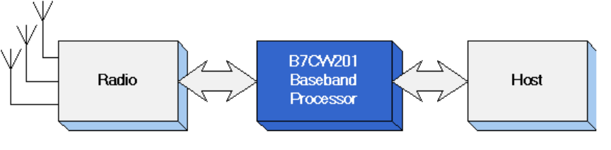
Figure 1. Windeo Block Diagram.................................................................................................................. 4
Figure 2. TX Test setup.................................................................................................................................. 8
Figure 3. TX/RX PER Test setup ……………………………………………………………………………….8
SIGMA DESIGNS Windeo Reference Design Module User Guide
Page 3/9
1. Introduction
This user’s guide provides information for operating the Windeo Reference Design Module. This
Reference board is the RF/Baseband UWB Transceiver using Sigma Windeo Chipset. The Windeo chip set
is based on the Wimedia Aliance Multi-band OFDM (MBOA) PHY v1.1 and MAC v1.0 Specifications and
is comprised of two devices:
• Windeo RF IC (B7CW101)
• Windeo Baseband IC (B7CW201)
The Reference Board supports PCI/SPI interface and is capable of transmit multiple HD video streams
over-the-air to multiple HDTVs simultaneously.
1.1 Sigma Chip set
1.1.1 Windeo Baseband IC (B7CW201)
The B7CW201 is divided into three main blocks.
1. Medium Access Control (MAC)
2. Physical Layer (PHY)
3. RF Macro (ADC, DAC and PLL)
The B7CW201 requires 33-MHz system clock supplied by an external oscillator from RF section. PLL use
this 33Mhz clock to generate 528Mhz clock require for ADC and DAC. Clock divider circuit generate all
required clocks for PHY and MAC.
1.1.2 Windeo RF IC (B7CW101)
• A RF transmitter and receiver for Ultra Wideband (UWB) frequencies
• Based on the WiMedia Alliance Multi-Band Orthogonal Frequency Division Modulation
(MBOFDM) communications Specifications for frequencies between 3168MHz
to 4752MHz
• Supports data rates up to 480Mbps
• Uses multiple receivers to permit non line-of-site reception with the Windeo® Baseband
B7CW201 processor device
• Supports the 3 MBOA Group 1 bands, centered at 3.43GHz, 3.96GHz and 4.48GHz,
with a bandwidth of 528MHz each.
• Supports Band hopping and the ability to select or change the channel
• Supports TFI and FFI modes
• Supports power save mode
• Only a single external resistor and RF baluns required
1.2 Main external components.
Main external components include:
• Flash
• SDRAM
• Regulators
• RF baluns
• RF BPFs
• T/R switch.
SIGMA DESIGNS Windeo Reference Design Module User Guide
Page 4/9
2. Theory of operation
Figure 1 Windeo Block Diagram
2.1 Transmit section:
2.1.1 Baseband Transmitter
2.1.1.1 MAC Packet Transmission
If the host is PCI, then Windeo supports a multi-packet and multi-fragment gather process. There are
no restrictions on the size or alignment of any of the packet buffer fragments. Furthermore,
fragmentation on one MSDU or MCDU (if needed) is supported through the effort of both the HW
and the CPU.
The following describes a typical transmit process.
1.Packets are handed to the driver by the OS, if PCI; or packet data comes from SPI channels.
2.Device driver prepares TX descriptor and programs the on-chip memory-mapped register files.
3.On detecting the newly prepared descriptor, the PCI bus master transmitter DMA extracts address
and length from the descriptor, initiates the PCI bus request, and transfers data from the host memory
into on-chip PCI TX FIFO.
4.When there are enough data words in the PCI_TX_FIFO, HostTxDma requests or prefetches a cell
pointer from the MacCpCtrl.
5.HostTxDma transfers the payload data from the PCI TX FIFO in to the external SDRAM, addressed
by the cell pointer.
6.Once the entire packet has been downloaded into the SDRAM, the data structure TCL (Transmit
Control List), consisting of frame length and the cell pointers associated with this packet is then sent
to TCL queue for later processing by the CPU. An interrupt is generated.
7.On receiving the interrupt, the CPU reads the data structures off the TCL queue and processes each
individual data structure. After finishing the processing of one data structure, the CPU writes the data
structure(s) to this frame’s stream queue in MacTxQScheduler for transmission (note that the CPU
also prepares the 16-byte of PLCP header and writes to the location that is pointed to by the MAC
frame header pointer).
8.The packet data goes through the CCM block and if the security service is enabled, then the
encrypted data is sent to the PHY through the WiMedia MAC-PHY interface protocol. This process
repeats until the entire packet is transmitted to the PHY. The FCS, calculated over the encrypted
payload, is appended at the end of payload and sent to the PHY as well.
SIGMA DESIGNS Windeo Reference Design Module User Guide
Page 5/9
9.Once the entire packet has been transmitted to the PHY and if no-ACK is indicated, MacTxDma
informs CPU of the completion of the transmission. In response, the CPU would pop the queue entry
and write the cell pointers to release buffer so that hardware can put them back to free pool of
pointers. If IMM-ACK is indicated, then TX_EN is deasserted and RX_EN is asserted. Within a
specified time interval, the expected ACK packet should arrive. If not, the frame may be re-
transmitted, or an interrupt may be generated and sent to CPU for further action.
2.1.1.2 PHY transmitter
The PHY Transmitter is designed to meet the WiMedia PHY standard, version 1.1a. Windeo
implements data rates 53.3 through 200 Mbps, with parameters summarized in the following table:
Data Rate and Other Parameters Implemented in Windeo (from WiMedia standard)
Data
Rate
(Mb/s)
Rate
Code
(R1-R5)
Modulation Code
Rate Conjugate
Symmetry
at IFFT
Input
Time
Spreading
Factor
(TSF)
Overall
Spreadin
g Gain
Coded
Bits/6 OFDM
Symbols
(NCBP6S)
Info Bits/6
OFDM
Symbols
(NIBP6S)
53.3 00000 QPSK 1/3 Yes 2 4 300 100
80 00001 QPSK 1/2 Yes 2 4 300 150
106.7 00010 QPSK 1/3 No 2 2 600 200
160 00011 QPSK 1/2 No 2 2 600 300
200 00100 QPSK 5/8 No 2 2 600 375
2.1.2 RF transmitter
The RFIC transmitter accepts both I and Q differential inputs from a pair of DACs on the
B7CW201 processor and contains I and Q base-band filters, up-converters and an on chip PA
(Power Amplifier).
The transmitter incorporates matched low pass filters in both the I and Q channels. The
base-band signal is up converted to an RF frequency through mixers driven by a VCO. As
in the receiver, the VCO frequency is selected through the band selection input pins
BAND[3:1]. The I and Q channel RF signals are combined in a summing circuit and
passed on to the power amplifier. The output of the power amplifier is differential with
each output presenting a nominal 50 Ohm impedance. The power amplifier must then be
matched to the 50 Ohm antenna load through a 2:1 balun. An external band-pass filter covering the
lower three bands of the UWB spectrum (3.1 –t 4.8 passband) is incorporated at the output of the
power amplifier. The UWB transmission will be sending to omnidirectional antenna via T/R switch
that allows Transceiver to operate in TDD mode.
SIGMA DESIGNS Windeo Reference Design Module User Guide
Page 6/9
2.2. Receive section:
2.2.1. RF receiver
The B7CW101 contains 3 receive channels. Each of the receiver channels provides both I
and Q outputs and contains an LNA (Low Noise Amplifier), down-converters, I and Q
base-band filters, variable gain amplifiers (VGA’s) and a final fixed gain block. All inputs
and outputs are differential. Each side of the differential RF input is nominally 50 Ohms.
So, the RF inputs are driven from an antenna through a 1:2 differential balun. Each side of
the RX outputs is a source follower with typically a 1.5mA source current.
Each receive channel has typically,
• 3.1GHz to 4.8GHz receive bandwidth
• Sensitivity of -80dBm
• Output capability of 560mV peak to peak for driving an ADC
• Independently controlled VGA gains
Each receiver LNA incorporates a band-pass filter which covers the lower 3 bands of the
UWB spectrum. The RF signal is down converted to a base-band frequency through mixers
driven by a VCO. The VCO frequency is selected through the band selection input pins
BAND[3:1] on the B7CW101. The base-band signal is then filtered and amplified through
the VGA blocks.
Each VGA provides a variable gain range of 31dB in 1dB steps. The 2 VGA’s within each
receiver channel (I and Q) always have the same gain, although the gain can be different
between channels. Each VGA is followed by a fixed gain block to provide a
low voltage, differential analog, output signal to an ADC on the B7CW201 Baseband processor.
2.2.2 Baseband Receiver
2.2.2.1 PHY Receiver
The Windeo PHY receiver of the Baseband chip features the 3-channel Intelligent Array Radio (IAR)
PHY receiver. The front ends and the back end together include all of the signal processing and
decoding blocks required for reliable reception of user data. The signal processing and decoding
functions implemented in the Windeo PHY receiver include the following:
•Packet detection and synchronization
•Automatic gain control
•Overlap-and-add
•Fast Fourier transform for OFDM demodulation
•Channel equalization
•Carrier frequency offset correction
•Sampling frequency offset correction
•Despreading, demapping, deinterleaving
•Viterbi decoding
SIGMA DESIGNS Windeo Reference Design Module User Guide
Page 7/9
•Descrambling
•Header decoding
•Receive signal strength calculation and reporting to MAC
•Link quality (SNR) calculation and reporting to MAC
•Error reporting to MAC
2.2.2.2 MAC Packet Reception
The Windeo supports a receive process where the incoming packets from the PHY are moved to the
system memory buffers.
The basic receive process is as follows.
1.While receiving an incoming packet, the MAC performs FCS check on the fly.
2.If the header error bit(s) is set, then the MAC HW discards the frame.
3.If the security bit is set in the frame header, then it performs the AES-128 decryption algorithm on
the incoming packet and further verifies the authentication tag. It checks for anti-replay as well.
4.Once the entire incoming packet data has been received into the SDRAM, the used cell pointer(s),
frame length, and other header information (in relation to the frame) are constructed as a Receive
Packet Status Descriptor (RxPSD) and the final RxPSD is pushed into RCL queue for further process
by the CPU. An interrupt event to the CPU could ensue.
5.Once the CPU is interrupted and processes the RxPSD, it forms the RDT for uploading. Note that
the CPU may have to perform re-assembly for the incoming packets, if needed.
6.On receiving the entries from RDT, HostRxDma makes request to SdramArb and transfers the data
to the targeted host device. The DMA checks the “More Fragments” bit and if it is set, it continues to
upload the second fragment, and so on. If the “More Fragment” is set to 0, the DMA completes the
uploading process for current MSDU or MCDU. If the fourth “More Fragment” bit in the current entry
is set to 1, the DMA then uses the “Next Pointer” to continue uploading the rest of the fragments
pertaining to the current MSDU or MCDU to the host. This process repeats until the HW sees the end
of fragment.
7.Once the entire MSDU data has been transferred to the host device, HostRxDma releases the index
to the CPU for re-cycling.
3. Software Control
Flash Memory
Flash memory used in Windeo baseband ASIC is an asynchronous, parallel, 8-bit data bus device, with a
size of 2MB. It stores boot code and micro code. Right after power on reset, NIOS both executes boot code
from flash memory and copies micro code from flash memory to SDRAM. Upon completion of this task,
NIOS executes its instruction from SDRAM.
SIGMA DESIGNS Windeo Reference Design Module User Guide
Page 8/9
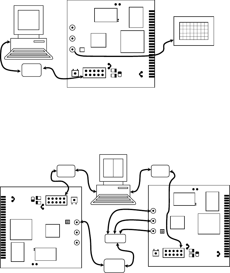
4. Test Configuration
Figure 2. TX test Setup
Figure 3. TX/RX PER Test Setup
DU
R
T/R
R
Windeo Mini
5GND
R
BBan
Flash
R
A
M
Res
Head
C9
SW
A
C
B
DU
R
T/R
R
Windeo
Mini
5
GND
RBBan
Flash R
A
M
Res Head
C9
SW
A
CB
1/10dB
step Atten
USB
Combiner
USB
DU
R
T/R
R
Windeo Mini
5
GND
RBBan
Flash R
A
M
Res Head
C9
SW
A
C B
LeCro
y
/S
p
ectrum
USB Blaste
r

SIGMA DESIGNS Windeo Reference Design Module User Guide
Page 9/9
5. Basic Test Procedure
1) Connect the DUT as shown in Fig.7 for TX quality test and Fig. 8 for TX/RX PER test .
a) With RF cable between T/Rx Port and LeCroy/Spectrum Analyzer
b) US blaster cable to JTAG header on DUT
c) DC Power to 5V pin
2) Load program “ XXXX” from computer and follow instructions from screen
Tx Packet Error Rate Tests
The spectral mask tests focus on whether the Tx signal falls within the WiMedia-specified
spectral mask, as determined using the LeCroy or other tester. A simple pass or fail should be
recorded based on the LeCroy measurement.
Tx Packet Error Rate Tests
Tx packet error rate tests require a previously tested reference PHY on the Rx side. As in the
WiMedia PHY test spec, these tests are carried out in a conducted (wired) environment with the
device under test in Tx mode and the reference PHY in Rx mode. The receive level should be set
to -50dBm. Below is a draft template for measurements. It is recommended that all tests be
carried out for packet lengths of 188, 1024, and 4088 bytes as indicated.
PHY data
rate
(Mbps)
Length(bytes) number of
packets
TFC PER, 1500 bytes
pass: < 0.01%
53.3 1500 10000 5
6
106.7 1500 10000 5
6
4) Rx Packet Error Rate Tests
Rx packet error rate tests require a previously tested reference PHY on the Tx side. As in the
WiMedia PHY test spec, these tests are carried out in a conducted (wired) environment with the
device under test in Rx mode and the reference PHY in Tx mode. Below is a draft template for
measurements. As indicated, all tests are to be carried out for Rx signal levels of -55 dBm and -65
dBm.
PHY data
rate (Mbps)
length (bytes) number of
packets
TFC PER, -55 dBm Rx
level
pass: < 1%
PER, -65 dBm Rx
level
pass: < 8%
53.3 1500 10000 5
6
106.7 1500 10000 5
6