Silicon Laboratories Finland EM35X2 ETRX35x-LR Series Zigbee Modules User Manual TG ETRX35x LR PM 011 102
Telegesis (UK) Ltd ETRX35x-LR Series Zigbee Modules TG ETRX35x LR PM 011 102
manual
Telegesis TG-ETRX35X-LR-PM-011-101
ETRX351-LR AND ETRX357-LR Preliminary Product Manual
©2010 Telegesis (UK) Ltd ETRX35x-LR Preliminary Product Manual
ETRX35x-LR ZIGBEE® MODULES
PRODUCT MANUAL

ETRX351-LR AND ETRX357-LR
©2010 Telegesis (UK) Ltd - 2 - ETRX35x-LR Preliminary Product Manual
Table of Contents
1 INTRODUCTION................................................................................................................... 5
1.1 Hardware Description ........................................................................................................ 5
2 PRODUCT APPROVALS..................................................................................................... 6
2.1 FCC Approvals...................................................................................................................6
2.1.1 FCC Labelling Requirements............................................................................................. 6
2.2 European Certification ....................................................... Error! Bookmark not defined.
2.3 Declarations of Conformity................................................. Error! Bookmark not defined.
2.4 IEEE 802.15.4.................................................................................................................... 6
2.5 The ZigBee® Protocol ....................................................................................................... 6
3 MODULE PINOUT................................................................................................................ 8
4 HARDWARE DESCRIPTION ............................................................................................. 10
4.1 Hardware Interface .......................................................................................................... 10
5 FIRMWARE DESCRIPTION............................................................................................... 11
5.1 Custom Firmware............................................................................................................. 11
5.2 Software Interface............................................................................................................ 12
6 ABSOLUTE MAXIMUM RATINGS..................................................................................... 13
7 RECOMMENDED OPERATING CONDITIONS ................................................................. 13
8 DC ELECTRICAL CHARACTERISTICS............................................................................ 14
9 DIGITAL I/O SPECIFICATIONS......................................................................................... 15
10 A/D CONVERTER CHARACTERISTICS ........................................................................... 16
11 AC ELECTRICAL CHARACTERISTICS............................................................................ 16
11.1 TX Power Characteristics ................................................................................................ 18
12 PHYSICAL DIMENSIONS .................................................................................................. 19
13 SOLDERING TEMPERATURE TIME PROFILE (FOR REFLOW SOLDERING) .............. 20
13.1 For Leaded Solder ........................................................................................................... 20
13.2 For Lead-free Solder........................................................................................................ 20
14 PRODUCT LABEL DRAWING........................................................................................... 21
15 RECOMMENDED FOOTPRINT ......................................................................................... 22
15.1 Example carrier board...................................................................................................... 23
16 RELIABILITY TESTS ......................................................................................................... 24
17 APPLICATION NOTES ...................................................................................................... 24
17.1 Safety Precautions........................................................................................................... 24
17.2 Design Engineering Notes ............................................................................................... 24
17.3 Storage Conditions .......................................................................................................... 25

ETRX351-LR AND ETRX357-LR
©2010 Telegesis (UK) Ltd - 3 - ETRX35x-LR Preliminary Product Manual
18 PACKAGING ...................................................................................................................... 25
18.1 Embossed Tape............................................................................................................... 25
18.2 Component Orientation.................................................................................................... 26
18.3 Reel Dimensions.............................................................................................................. 26
18.4 Packaging ........................................................................................................................ 26
19 ORDERING INFORMATION .............................................................................................. 27
20 TRADEMARKS................................................................................................................... 28
21 DISCLAIMER......................................................................................................................28
22 ROHS DECLARATION....................................................................................................... 28
23 DATA SHEET STATUS...................................................................................................... 28
24 LIFE SUPPORT POLICY.................................................................................................... 28
25 RELATED DOCUMENTS................................................................................................... 29
26 CONTACT INFORMATION ................................................................................................ 29
ETRX351-LR AND ETRX357-LR
©2010 Telegesis (UK) Ltd - 4 - ETRX35x-LR Preliminary Product Manual
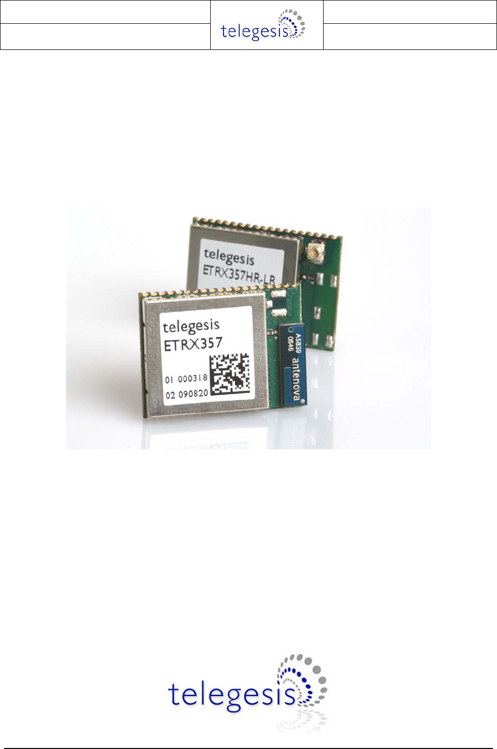
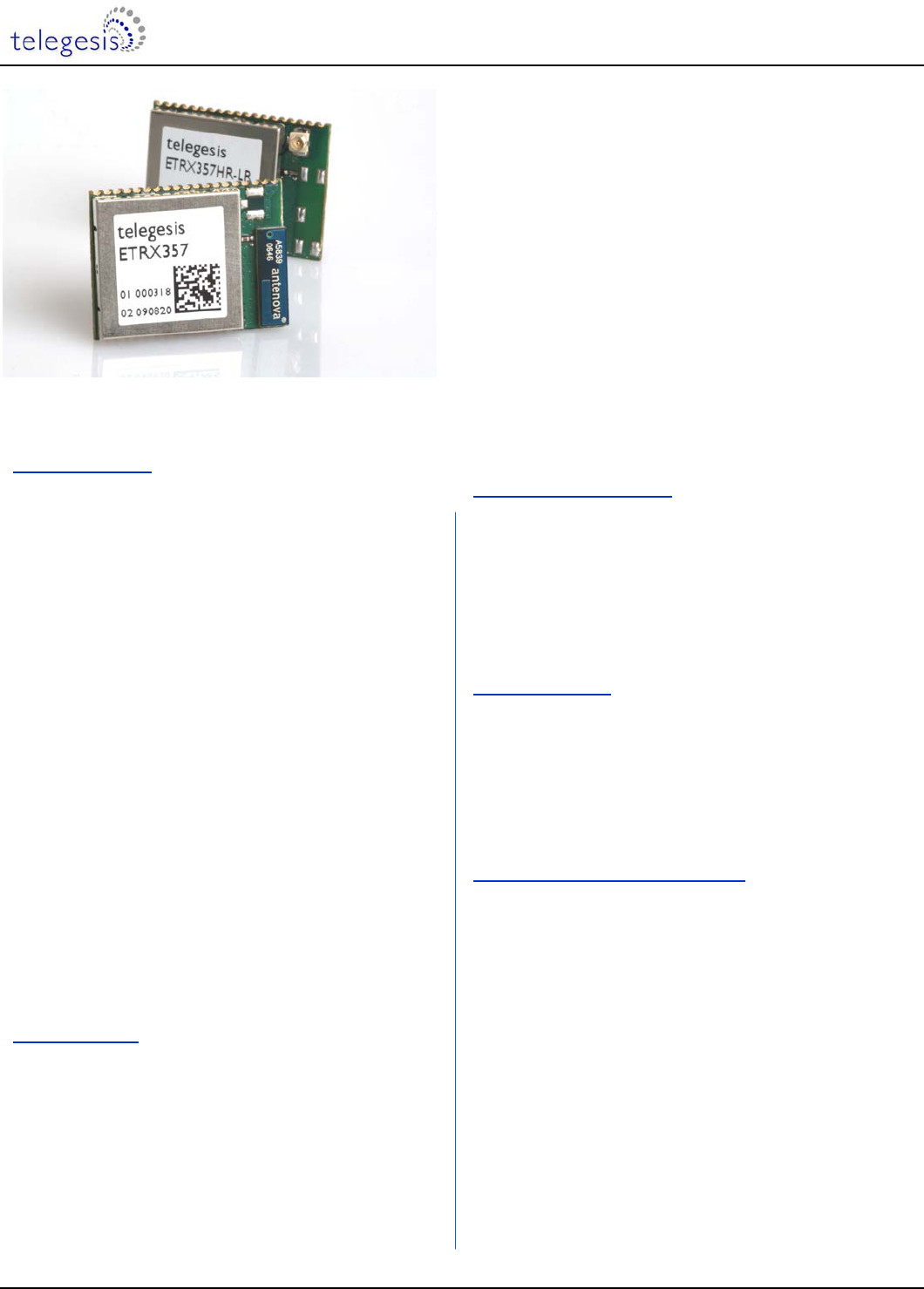
The Telegesis ETRX351-LR and ETRX357-LR modules
are low power 2.4GHz ZigBee modules with an added PA
and LNA for highest possible link budget.
Based on the latest Ember EM351 and EM357 single chip
ZigBeeTM solution the new long range modules are footprint
compatible with the ETRX351 and ETRX357, thus
representing a drop-in replacement for all applications
where a high link budget is required.
The module’s unique AT-style command line interface
allows designers to quickly integrate ZigBee technology
without complex software engineering. For custom
application development the ETRX35x series integrates
with ease into Ember’s InSi
g
ht develo
p
ment environment.
Image not shown actual size; enlarged to show detail.
Module Features
• Small form factor, SMT module 25mm x 19mm
• Side Castellations for easy soldering and inspection
• 2 antenna options: Integrated chip antenna or U.FL
coaxial connector
• Industry’s first ARM® Cortex-M3 based family of ZigBee
modules
• Industry standard JTAG Programming and real time
network level debugging via the Ember InSight Port
• 192kB (ETRX357) and 128kB (ETRX351) flash and
12kbytes of RAM
• Lowest Deep Sleep Current of sub 1µA and multiple
sleep modes
• Wide supply voltage range (2.1 to 3.5V)
• 32.768kHz watch crystal can be added externally
• Module ships with standard Telegesis AT-style
command interface based on the ZigBee PRO feature
set
• Can act as an End Device, Router or Coordinator
• 24 general-purpose I/O lines including analogue inputs
(all GPIOs of the EM35x are accessible)
• Firmware upgrades via serial port or over the air
(password protected)
• Hardware supported encryption (AES-128)
• CE and FCC compliance, FCC modular approval
pending
• Operating temperature range: -40°C to +85°C
• Standard version without LNA and PA available in the
same form factor
Radio Features
• Based on the Ember EM351 and EM357 single chip
ZigBeeTM / IEEE802.15.4 solutions
• 2.4GHz ISM Band
• 250kbit/s over the air data rate
• 16 channels (IEEE802.15.4 Channel 11 to 26)
• +18dBm output power (adjustable down to -21dBm)
• High sensitivity of -105dBm typ. @ 1% packet error rate
• RX Current: 28mA, TX Current: approx 100mA at
18dBm
• Robust Wi-Fi and Bluetooth coexistence
Suggested Applications
• AMR – ZigBee Smart Energy applications
• Wireless Alarms and Security
• Home/Building Automation
• Wireless Sensor Networks
• M2M Industrial Controls
• Lighting and ventilation control
• Remote monitoring
• Environmental monitoring and control
Development Kit
• New Development kit containing everything required to
set up a mesh network quickly and evaluate range and
performance of the ETRX35x and its long range
version.
• AT-style software interface command dictionary can be
modified for high volume customers.
• Custom software development available upon request.
Example AT-Style Commands
AT+BCAST Send a Broadcast
AT+UCAST:<address> Send a Unicast
AT+EN Establish PAN network
AT+JN Join PAN
At power-up the last configuration is loaded from non-
volatile S-Registers, which can eliminate the need for an
additional host controller.

ETRX351-LR AND ETRX357-LR
©2010 Telegesis (UK) Ltd - 5 - ETRX35x-LR Preliminary Product Manual
1 Introduction
This document describes the Telegesis ETRX351-LR and ETRX357-LR ZigBee® long range
modules which have been designed to be easily integrated into another device and to provide a
fast, simple and low cost wireless mesh networking interface.
The Telegesis ETRX3 series modules are based on the Ember ZigBee® platform consisting of the
single chip EM351 or EM357 combined with the ZigBee PRO compliant EmberZNet meshing
stack. Integration into a wide range of applications is made easy using a simple AT style
command interface and advanced hardware design.
The configurable functionality of the Telegesis AT Commandset often allows the ETRX3 series
ZigBee modules to be used without an additional host microcontroller saving even more integration
time and costs. In addition to the Telegesis AT Commandset, the ETRX351-LR and ETRX357-LR
modules can be used with custom-built firmware and they represent an ideal platform for custom
firmware development in conjunction with the Ember development kits. The ETRX3 series shares
the same R3xx Telegesis firmware as the ETRX2 and the two devices can be used in the same
network.
No RF experience or expertise is required to add this powerful wireless networking capability to
your products. The ETRX351-LR and ETRX357-LR offer fast integration opportunities and the
shortest possible time to market for your product.
1.1 Hardware Description
The main building blocks of the ETRX351-LR and ETRX357-LR are the single chip EM351 and
EM357 from Ember, a Power Amplifier as well as a Low Noise Amplifier, a 24MHz reference
crystal and RF front-end circuitry optimized for best RF performance. The modules are available
with on-board antenna or alternatively a U.FL connector for attaching external antennae. Modules
with the U.FL connector are identified by the “HR” suffix.
The LNA and RF power amplifier of the LR devices improve the output power by 10dB and the
sensitivity by 5dB which will increase the range by approximately 600% relative to the standard
devices (where local regulations permit the use of the maximum output power).
The integrated antenna is an Antenova Rufa, and details of the radiation pattern etc are available
from the Antenova website [5].
Module Chip Flash RAM
ETRX351-LR EM351 128kB 12kB
ETRX351HR-LR EM351 128kB 12kB
ETRX357-LR EM357 192kB 12kB
ETRX357HR-LR EM357 192kB 12kB
Table 1: Memories
The ETRX351-LR and ETRX357-LR are used for ZigBee® (www.zigbee.org) applications. If you
wish to create your own custom firmware, and not use the pre-loaded Telegesis AT-Command
interface, you will need the InSight toolchain, consisting of InSight Desktop™ together with a
comprehensive integrated development environment (IDE) and C-language compiler toolchain
from Ember. The Ember development environment is not suitable for an 802.15.4-only application
that does not use the ZigBee layer.
ETRX351-LR AND ETRX357-LR
©2010 Telegesis (UK) Ltd - 6 - ETRX35x-LR Preliminary Product Manual
2 Product Approvals
The ETRX351-LR and ETRX357-LR have been designed to meet all national regulations for world-
wide use. In particular the following certifications have been obtained:
2.1 FCC Approvals
The Telegesis ETRX351-LR and ETRX357-LR with integrated Antenna has been tested to comply
with FCC CFR Part 15 (USA). The devices meet the requirements for modular transmitter
approval as detailed in the FCC public notice DA00.1407.transmitter.
This device complies with Part 15 of the FCC rules. Operation is subject to the following
two conditions: (1) this device may not cause harmful interference, and (2) this device must
accept any interference received, including interference that may cause undesired
operation.
While the applicant for a device into which the ETRX351-LR or ETRX357-LR or ETRX351HR-LR is
installed is not required to obtain a new authorization for the module, this does not preclude the
possibility that some other form of authorization or testing may be required for the end product.
The FCC requires the user to be notified that any changes or modifications made to this device
that are not expressly approved by Telegesis (UK) Ltd. may void the user's authority to operate the
equipment.
2.2 FCC Labelling Requirements
When integrating the ETRX351-LR or ETRX357-LR into a product if must be ensured that the FCC
labelling requirements are met. This includes a clearly visible label on the outside of the finished
product specifying the Telegesis FCC identifier (FCC ID: S4GEM35X2) as well as the notice
above. This exterior label can use wording such as “Contains Transmitter Module FCC ID:
S4GEM35X2” or “Contains FCC ID: S4GEM35X2” although any similar wording that expresses
the same meaning may be used.
2.3 IEEE 802.15.4
IEEE 802.15.4 is a standard for low data rate, wireless networks (raw bit-rate within a radio packet
of 250kbps @2.4GHz) which focuses on low cost, low duty cycle, long primary battery life
applications as well as mains-powered applications. It is the basis for the open ZigBee® Protocol.
2.4 The ZigBee® Protocol
The ZigBee® Protocol is a set of standards for wireless connectivity for use between any devices
over short to medium distances. The specification was originally ratified in December 2004, paving
the way for companies to start making low-power networks a reality.
ZigBee® uses an IEEE 802.15.4 radio specification running on the 2.4GHz band, plus three
additional layers for networking, security and applications. What makes the specification unique is
its use of a mesh network architecture which, in bucket chain style, passes data from one node to
the next until it lands at its destination. The network is self-healing and adapts its routing as link
quality changes or nodes move. Furthermore, nodes can be defined as End Devices which do not
act as routers, but can therefore be put into a low-power sleep state.
FCC ID: S4GEM35X2

ETRX351-LR AND ETRX357-LR
©2010 Telegesis (UK) Ltd - 7 - ETRX35x-LR Preliminary Product Manual
The enhanced version of the ZigBee® standard (or ZigBee® 2006) was released in December
2006, adding new features and improvements to the only global wireless communication standard
enabling the development of easily deployable low-cost, low-power, monitoring and control
products for homes, commercial buildings and industrial plant monitoring. In 2007 the ZigBee
Alliance introduced the PRO featureset which offers advantages over earlier versions, including
• Truly self healing mesh networking
• Messages can now travel up to 30 hops
• Source-Routing for improved point to multipoint message transmission
• Improved security including Trust-Centre link keys
• New message types and options
The Telegesis AT Commandset, which by default ships on all ETRX3 series products is based on
the ZigBee PRO featureset. For more information on the Telegesis AT Commandset please refer
to the separate documentation at www.telegesis.com.
ETRX351-LR AND ETRX357-LR
©2010 Telegesis (UK) Ltd - 8 - ETRX35x-LR Preliminary Product Manual
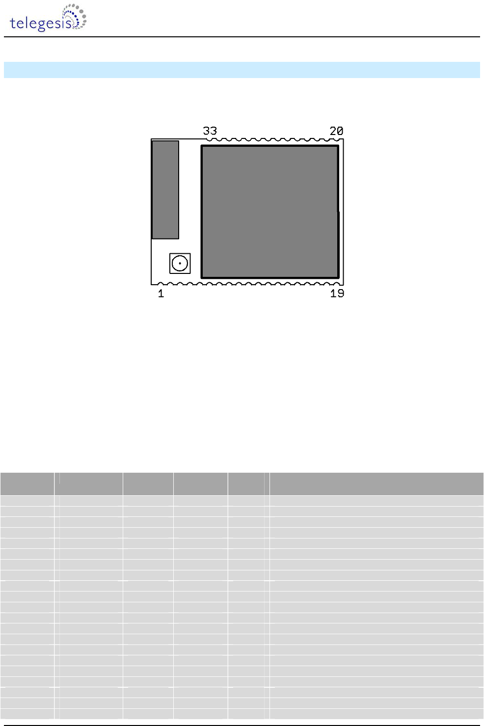
3 Module Pinout
Figure 1: ETRX3 series Module Pinout (top view)
The table below gives details about the pin assignment for direct SMD soldering of the ETRX3
series modules to the application board. For more information on the alternate functions please
refer to [2]. Also refer to the Telegesis AT Commandset documentation to understand how the pre-
programmed firmware makes use of the individual I/Os.
All GND pads are connected within the module, but for best RF performance all of them should be
grounded externally.
ETRX35x
pad Designation Normal
function Alternate
function EM35x
pin Ember designation
1 GND GND GND
2 PC5 {1} I/O 11 TX_ACTIVE
3 PC6 I/O 13 OSC32B, nTX_ACTIVE
4 PC7 I/O 14 OSC32A, OSC32_EXT
5 PA7 {4} I/O 18 TIM1C4
6 PB3 {2} I/O CTS 19 SC1nCTS, SC1SCLK, TIM2C3
7 nReset nReset 12
8 PB4 {2} I/O RTS 20 TIM2C4, SC1nRTS, SC1nSSEL
9 PA0 I/O 21 TIM2C1, SC2MOSI
10 PA1 I/O 22 TIM2C3, SC2SDA, SC2MISO
11 PA2 I/O 24 TIM2C4, SC2SCL, SC2SCLK
12 PA3 I/O 25 SC2nSSEL, TRACECLK, TIM2C2
13 GND GND GND
14 PA4 I/O 26 ADC4, PTI_EN, TRACEDATA
15 PA5 {3} I/O 27 ADC5, PTI_DATA, nBOOTMODE, TRACEDATA3
16 PA6 {4} I/O 29 TIM1C3
17 PB1 TXD 30 SC1MISO, SC1MOSI, SC1SDA, SC1TXD, TIM2C1
18 PB2 RXD 31 SC1MISO, SC1MOSI, SC1SCL, SC1RXD, TIM2C2
19 GND GND GND
20 GND GND GND
21 JTCK JTCK 32 SWCLK

ETRX351-LR AND ETRX357-LR
©2010 Telegesis (UK) Ltd - 9 - ETRX35x-LR Preliminary Product Manual
ETRX35x
pad Designation Normal
function Alternate
function EM35x
pin Ember designation
22 PC2 I/O 33 JTDO, SWO
23 PC3 I/O 34 JTDI
24 PC4 I/O 35 JTMS, SWDIO
25 PB0 I/O 36 VREF, IRQA, TRACECLK, TIM1CLK, TIM2MSK
26 PC1 I/O ADC3 38 ADC3, SWO, TRACEDATA0
27 PC0 {4} I/O 40 JRST, IRQD, TRACEDATA1
28 PB7 {4} I/O ADC2 41 ADC2, IRQC, TIM1C2
29 PB6 {4} I/O ADC1 42 ADC1, IRQB, TIM1C1
30 PB5 I/O ADC0 43 ADC0, TIM2CLK, TIM1MSK
31 GND GND GND
32 Vcc Vcc Vcc
33 GND GND GND
Table 2. Pin Information
Alternate functions depend on the firmware, but the R3xx functions are indicated here for
convenience.
Notes:
{1} PC5 is not usable on these long range versions of the ETRX35x as this GPIO is used as
TX_ACTIVE to control the external RF frontend.
{2} When using the Telegesis AT Commandset, RTS/CTS handshaking is selectable in firmware. See
the AT Command Manual.
{3} If PA5 is driven low at power-up or reset the module will boot up in the bootloader
{4} PA6, PA7, PB6, PB7 and PC0 can drive high current (see section 9)
ETRX351-LR AND ETRX357-LR
©2010 Telegesis (UK) Ltd - 10 - ETRX35x-LR Preliminary Product Manual
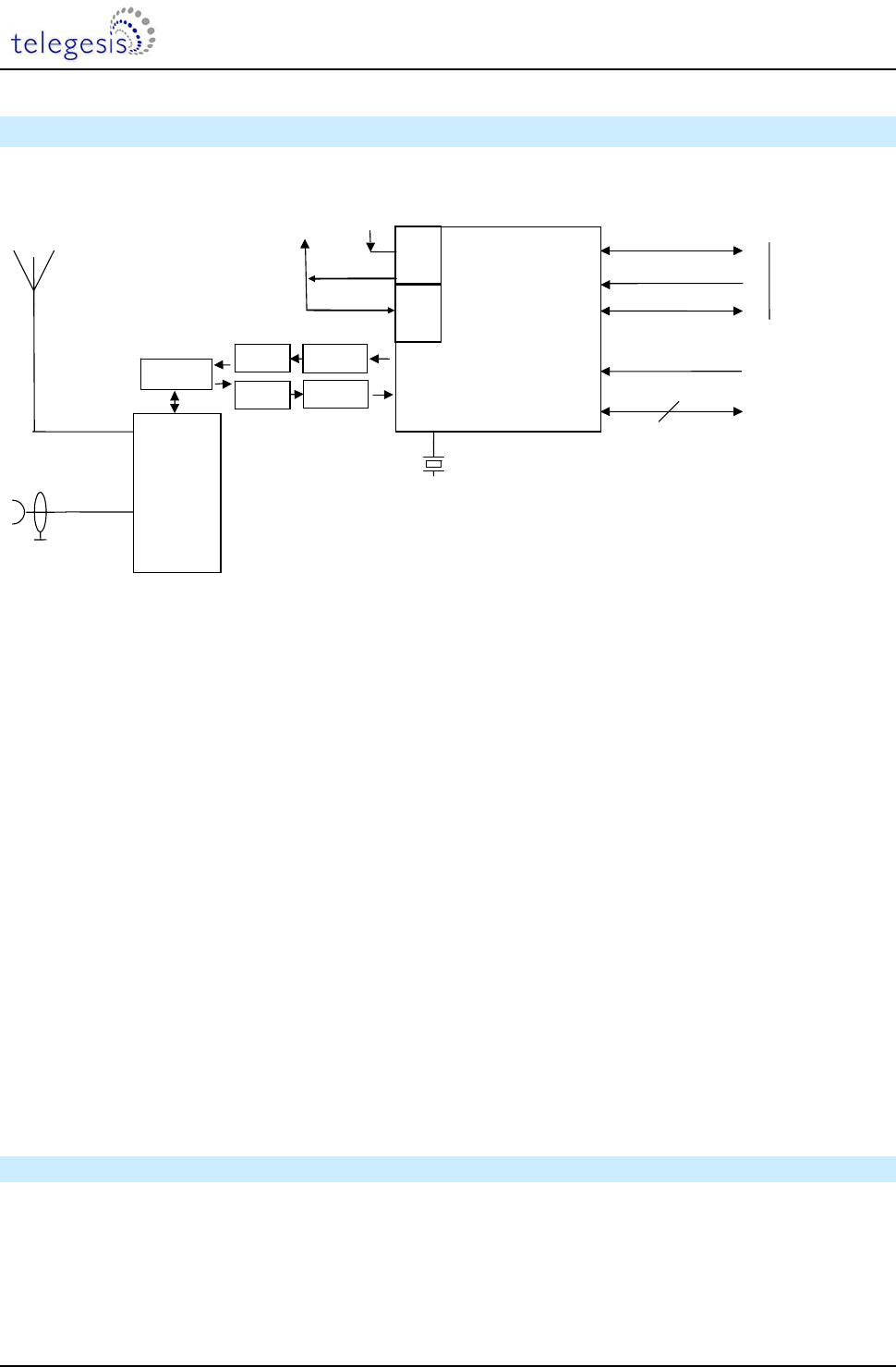
4 Hardware Description
24MHz
EM35x
I/O
UART
I / O
programming
5JTAG
Vcc
Vreg
RESET
RESET
Balun
integrated
antenna
U.FL socket
rf
terminal
selection,
filtering and
matching
circuitry
LDO
1V8
1,8Vdc
A
/D
LDO
1V25
Balun
PA
LNA
Switch
Figure 2: Hardware Diagram
The ETRX351-LR and ETRX357-LR are based on the Ember EM351 and EM357 respectively in
addition to a discrete PA, LNA and RF switch added to the RF-Frontend. The EM351 and EM357
are fully integrated 2.4GHz ZigBee transceivers with a 32-bit ARM® Cortex M3TM microprocessor,
flash and RAM memory, and peripherals.
The industry standard serial wire and JTAG programming and debugging interfaces together with
the standard ARM system debug components help to streamline any custom software
development.
In addition to this a number of MAC functions are also implemented in hardware to help maintain
the strict timing requirements imposed by the ZigBee and IEEE802.15.4 standards.
The new advanced power management features allow faster wakeup from sleep and new power
down modes allow this 3rd generation module to offer a longer battery life than any 2nd generation
modules on the market.
The EM35x has fully integrated voltage regulators for both required 1.8V and 1.25V supply
voltages. The voltages are monitored (brown-out detection) and the built in power-on-reset circuit
eliminates the need for any external monitoring circuitry. A 32.768kHz watch crystal can be
connected externally to pads 3 and 4 in case more accurate timing is required.
4.1 Hardware Interface
All GPIO pins of the EM351 or EM357 are accessible on the module’s pads. Whether signals are
used as general purpose I/Os, or assigned to a peripheral function like ADC is set by the firmware.
When using the Telegesis AT Commandset please refer to the AT Commandset manual for this
information and when developing custom firmware please refer to the EM35x datasheet.

ETRX351-LR AND ETRX357-LR
©2010 Telegesis (UK) Ltd - 11 - ETRX35x-LR Preliminary Product Manual
5 Firmware Description
The modules will be pre-loaded with a standalone bootloader which supports over-the-air
bootloading as well as serial bootloading of new firmware.
In order to enter the standalone bootloader using a hardware trigger pull PA5 to ground and
power-cycle or reset the module. To avoid entering the standalone bootloader unintentionally
make sure not to pull this pin down during boot-up unless the resistance to ground is >10k. (A
pull-up is not required).
In addition to the standalone bootloader the modules also contain the current release of the
Telegesis AT-style command interface as described in the Telegesis AT command dictionary and
the Telegesis user guide. Check www.telegesis.com for updates. Each module comes with a
unique 64-bit 802.15.4 identifier which is stored in non-volatile memory. The commands and
responses pass through the serial port of the ETRX35x-LR as ASCII text, so a simple terminal
application will usually suffice. We provide Telegesis Terminal but it is not an essential feature.
The pre-loaded AT-style command interface firmware is based on the latest EmberZNet meshing
stack which implements routers/coordinators as well as (sleepy) end devices. [End devices have
no routing responsibility and therefore are allowed to go to sleep, whilst still being able to send and
receive messages via a parent router. In addition to a classical (sleepy) end device the module
firmware also supports mobile (sleepy) end devices capable of changing their parent quickly
whenever they change their position within the network.]
A router is typically a mains powered device whilst a sleepy end device (SED) can be battery
powered.
The module is also able to act as a PAN coordinator and Trust Centre through external host
control. The AT style command line supplies all the tools required to set up and manage a ZigBee
network by allowing easy access to the low-level functionality of the stack.
The Telegesis firmware uses the meshing and self healing EmberZNet PRO stack to overcome
many of the limitations of the tree network topology of the ZigBee® 2006 stack by using the ZigBee
PRO featureset.
The Telegesis firmware also allows low-level access to physical parameters such as channel and
power level. Parameters that define the functionality of the ETRX35x module and also allow
standalone functionality are saved in non-volatile memory organised in so-called S-Registers. The
SPI and I2C buses are not supported by the current firmware release, but can be used with custom
firmware.
5.1 Custom Firmware
For high volume customers the firmware can be customised on request. Customers can use the
ETRX35x module as hardware only and develop their own firmware based on the EmberZNet
stack. In order to develop custom firmware the Ember Insight toolchain is required.

ETRX351-LR AND ETRX357-LR
©2010 Telegesis (UK) Ltd - 12 - ETRX35x-LR Preliminary Product Manual
5.2 Software Interface
Using the default firmware the ETRX35x-LR is controlled using a simple AT-style command
interface and (mostly) non-volatile S-Registers. In order to get a full listing of all the available AT-
Commands, please refer to the AT command dictionary document which corresponds to the
firmware revision you intend to use.
In addition to the command dictionary there are user guides explaining the features of the firmware
in more detail. If you need to find out which firmware resides on your module simply type “ATI”
followed by a carriage return and you will be prompted with the module’s manufacturing
information.
The Development Kit manual describes how to upgrade the firmware either via a serial link or over
the air.
ETRX351-LR AND ETRX357-LR
©2010 Telegesis (UK) Ltd - 13 - ETRX35x-LR Preliminary Product Manual
6 Absolute Maximum Ratings
Supply: 3.5V
Inputs: -0.3V to Vcc + 0.3V
Operating temperature: -40 to 85°C
No. Item Symbol Absolute Maximum Ratings Unit
1 Supply voltage VCC -0.3 to +3.5 Vdc
2
Voltage on any I/O[11:0] ,
SIF_CLK, SIF_MISO, SIF_MOSI,
SIF_LOADB, RESET
Vin -0.3 to VCC +0.3 Vdc
3 Storage temperature range Tstg -40 to +105 °C
4 Operating temperature range Top -40 to +85 °C
5 Input RF level Pmax 15 dBm
6
ESD on any pin {1} according to
Human Body Model (HBM) circuit
description
VTHHBM ±2 kV
7 Reflow temperature TDeath Please refer to chapter 13 °C
Table 3. Absolute Maximum Ratings
Note:
{1} Input must be current limited to the value specified.
The absolute maximum ratings given above should under no circumstances be violated.
Exceeding one or more of the limiting values may cause permanent damage to the device.
Caution! ESD sensitive device. Precautions should be used when handling the device
in order to prevent permanent damage.
7 Recommended Operating Conditions
No. Item Condition /
Remark Symbol Value Unit
Min Typ Max
1 Supply voltage VCC 2.1 3.5 Vdc
2 RF Input Frequency fC 2405 2480 MHz
3 RF Input Power pIN 0 dBm
4 Operating temperature
range Top -40 +85 °C
Table 4. Recommended Operating Conditions
ETRX351-LR AND ETRX357-LR
©2010 Telegesis (UK) Ltd - 14 - ETRX35x-LR Preliminary Product Manual
8 DC Electrical Characteristics
VCC = 3.0V, TAMB = 25°C, NORMAL MODE unless otherwise stated
No. Item Condition /
Remark Symbol Value Unit
Min Typ Max
1 Module supply voltage VCC 2.1 3.5 Vdc
2
Quiescent current,
internal RC oscillator
disabled
ISLEEP 2.4 µA
3
Quiescent current,
internal RC oscillator
enabled
ISLEEP 2.8 µA
4
Quiescent current,
including
32.768kHz oscillator
ISLEEP 3.3 µA
5 Transmit current
consumption
at +18dBm
module output
power
ITXVCC 90 mA
6
Transmit Current
consumption
BOOST MODE
at +18dBm
module output
power
ITXVCC 100 mA
7 Transmit current
consumption
at min. module
output power ITXVCC tbd mA
8 Receive current
consumption
Total, 12MHz
clock speed IRX 30 mA
9 Receive current
consumption
Total, 24MHz
clock speed IRX 31 mA
10
Receive current
consumption
BOOST MODE
Total, 12MHz
clock speed IRX 31 mA
11
Receive current
consumption
BOOST MODE
Total, 24MHz
clock speed IRX 32 mA
12 MCU, RAM and flash,
radio off
12MHz clock
speed IMCU 7 mA
13 MCU, RAM and flash,
radio off
24MHz clock
speed IMCU 8 mA
14 Serial Controller Max data rate ISC 0.2 mA
15 Timer Max clock rate ITMR 0.25 mA
16 ADC Max sample rate IADC 1.1 mA
17 Wake time from deep
sleep
From wakeup
event to 1st
instruction
100 µs
18 Shutdown time
From last
instruction into
deep sleep
5 µs
Table 5. DC Electrical Characteristics
Please Note: The average current consumption during operation is dependent on the firmware
and the network load, therefore these figures are given in the command dictionary of the
respective firmware.

ETRX351-LR AND ETRX357-LR
©2010 Telegesis (UK) Ltd - 15 - ETRX35x-LR Preliminary Product Manual
9 Digital I/O Specifications
The digital I/Os of the ETRX35x module have the ratings shown below.
VCC = 3.0V, TAMB = 25°C, NORMAL MODE unless otherwise stated
No. Item Condition /
Remark Symbol Value Unit
Min Typ Max
1 Low Schmitt switching
threshold
Schmitt input
threshold going
from high to low
VSWIL 0.42 x VCC 0.5 x VCC Vdc
2 High Schmitt switching
threshold
Schmitt input
threshold going
from low to high
VSWIH 0.62 x VCC 0.8 x VCC MHz
3 Input current for logic 0 IIL -0.5 µA
4 Input current for logic 1 IIH 0.5 µA
5 Input Pull-up resistor
value RIPU 24 29 34 k
6 Input Pull-down resistor
value RIPD 24 29 34 k
7 Output voltage for logic 0
IOL = 4mA (8mA) for
standard (high
current) pads
VOL 0 0.18 x VCC V
8 Output voltage for logic 1
IOH = 4mA (8mA)for
standard (high
current) pads
VOH 0.82 x VCC VCC V
9 Output Source Current Standard current
pad IOHS 4 mA
10 Output Sink current Standard current
pad IOLS 4 mA
11 Output Source Current High current pad IOHH 8 mA
12 Output Sink current High current pad IOLH 8 mA
13 Total output current IOH + IOL 40 mA
Table 6. Recommended Operating Conditions
ETRX351-LR AND ETRX357-LR
©2010 Telegesis (UK) Ltd - 16 - ETRX35x-LR Preliminary Product Manual
10 A/D Converter Characteristics
The ADC is a first-order sigma-delta converter. For additional information on the ADC please refer
to section 10 of the EM35x datasheet.
No. Item
1 A/D resolution Up to 12 bits
2 A/D sample time for 5-bit conversion 5.33µs
3 A/D sample time for 12-bit conversion 682µs
4 Reference Voltage 1.25V or Vcc
Table 7. A/D Converter Characteristics
11 AC Electrical Characteristics
VCC = 3.0V, TAMB = 25°C, NORMAL MODE measured at 50Ω terminal load connected to the U.FL socket
No. Receiver Value Unit
Min Typ Max
1 Frequency range 2400 2500 MHz
2 Sensitivity for 1% Packet Error Rate (PER) -106 -105 -99 dBm
3 Sensitivity for 1% Packet Error Rate (PER) BOOST MODE -106 -105 -100 dBm
4 Saturation (maximum input level for correct operation) 0 dBm
5 High-Side Adjacent Channel Rejection
(1% PER and desired signal –82dBm acc. to [1]) 35 dB
6 Low-Side Adjacent Channel Rejection
(1% PER and desired signal –82dBm acc. to [1]) 35 dB
7 2nd High-Side Adjacent Channel Rejection
(1% PER and desired signal –82dBm acc. to [1]) 43
8 2nd Low-Side Adjacent Channel Rejection
(1% PER and desired signal –82dBm acc. to [1]) 43
9 Channel Rejection for all other channels
(1% PER and desired signal –82dBm acc. to [1]) 40 dB
10 802.11g rejection centred at +12MHz or –13MHz
(1% PER and desired signal –82dBm acc. to [1]) 35 dB
11 Co-channel rejection
(1% PER and desired signal –82dBm acc. to [1]) -6 dBc
12 Relative frequency error
(2x40ppm required by [1]) -120 120 ppm
13 Relative timing error
(2x40ppm required by [1]) -120 120 ppm
14 Linear RSSI range 35 dB
15
Output power at highest power setting
NORMAL MODE
BOOST MODE
16
17
18
18
19
19 dBm
16 Output power at lowest power setting tbd dBm
17 Error vector magnitude as per IEEE802.15.4 7 15 %
18 Carrier frequency error -40 40 ppm
19 PSD mask relative
3.5MHz distance from carrier -20 dB
20 PSD mask absolute
3.5MHz distance from carrier -30 dBm
Table 8. AC Electrical Characteristics
ETRX351-LR AND ETRX357-LR
©2010 Telegesis (UK) Ltd - 17 - ETRX35x-LR Preliminary Product Manual
Please Note: For the relationship between EM35x power settings and module output power
please relate to chapter 11.1 of this document. When developing custom firmware the output
power settings described in this document relate directly to the EM35x power settings accessible
via the Ember stack API.
No. Synthesiser Characteristics Limit Unit
Min Typ Max
22 Frequency range 2400 2500 MHz
23 Frequency resolution 11.7 kHz
24 Lock time from off state, with correct VCO DAC settings 100 µs
25 Relock time, channel change or Rx/Tx turnaround 100 µs
26 Phase noise at 100kHz offset -71dBc/Hz
27 Phase noise at 1MHz offset -91dBc/Hz
28 Phase noise at 4MHz offset -103dBc/Hz
29 Phase noise at 10MHz offset -111dBc/Hz
Table 9. Synthesiser Characteristics
No. Power On Reset (POR) Specifications Limit Unit
Min Typ Max
30 VCC POR release 0.62 0.95 1.2 Vdc
31 VCC POR assert 0.45 0.65 0.85 Vdc
Table 10. Power On Reset Specifications
No. nRESET Specifications Limit Unit
Min Typ Max
32 Reset Filter Time constant 2.1 12 16 µs
33 Reset Pulse width to guarantee a reset 26 µs
34 Reset Pulse width guaranteed not to cause reset 0 1 µs
Table 11. nReset Specifications

ETRX351-LR AND ETRX357-LR
©2010 Telegesis (UK) Ltd - 18 - ETRX35x-LR Preliminary Product Manual
11.1 TX Power Characteristics
Important Note: For Band edge compliance it is required to limit the output power out of the
EM357 on channel 26 to a setting of -22dBm. Because of this it is recommended to not use
channel 26 on the ETRX35x-LR modules as the range will be significantly reduced on this channel.
The diagrams below show the typical output power and module current in dependency on module
supply voltage and EM35x power setting in NORMAL MODE and BOOST MODE.
Figure 3. Output Power vs. Power Setting
Figure 4. Output Power vs. Power Setting
Figure 5. Module Current vs. Power Setting
Figure 6. Output Power vs. Power Setting (BOOST MODE)
Figure 7. Module Current vs. Power Setting (BOOST MODE)
t.b.d
t.b.d
t.b.d
t.b.d
t.b.d
ETRX351-LR AND ETRX357-LR
©2010 Telegesis (UK) Ltd - 19 - ETRX35x-LR Preliminary Product Manual
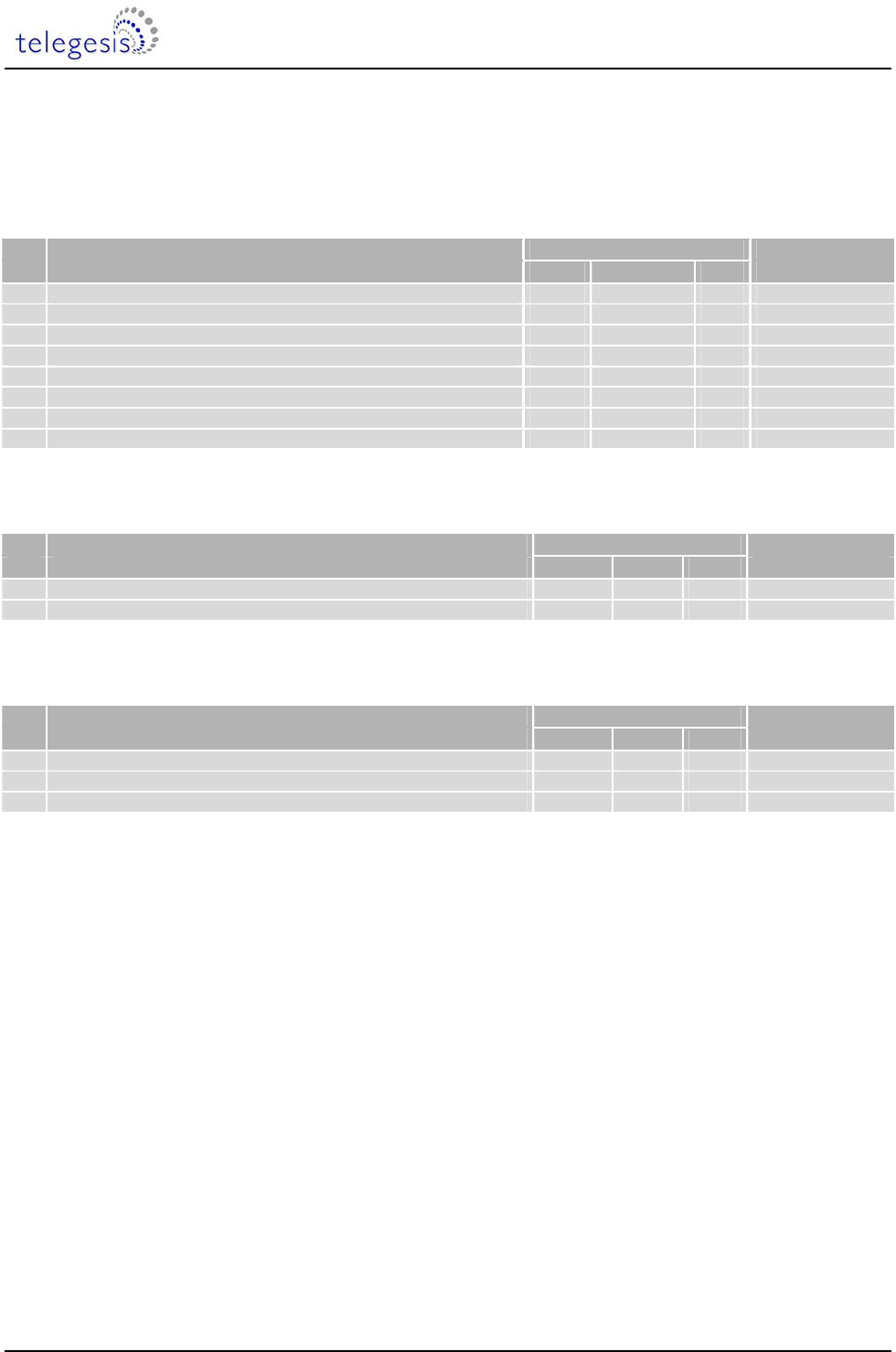
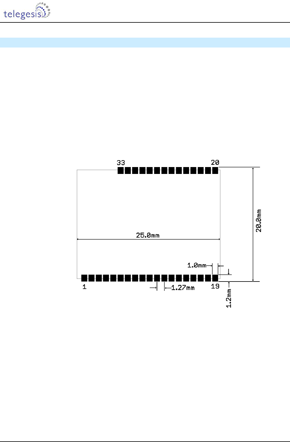
12 Physical Dimensions
Figure 8. ETRX3 Physical Dimensions
Symbol Explanation Distance
L Length of the module 25.0mm
W Width of the module 19.0mm
H Height of the module 3.0mm
A1 Distance centre of pad PCB edge 0.9mm
A2 Pitch 1.27mm
R1 Keep-out Zone from corner of PCB 17.5mm
R2 Keep-out Zone from corner of PCB 4.1mm
X1 Distance centre of Antenna connector PCB edge 3.8mm
X2 Distance centre of Antenna connector PCB edge 2.8mm
Table 12. ETRX3 Physical Dimensions
For ideal RF performance when using the on-board antenna, the antenna should be located at the
corner of the carrier PCB. There should be no components, tracks or copper planes in the “keep-
out” area which should be as large as possible. When using the U.FL RF connector the “keep-out”
area doesn’t have to be kept. NB: The module transmit/receive range will depend on the antenna
used and also the housing of the finished product.
ETRX351-LR AND ETRX357-LR
©2010 Telegesis (UK) Ltd - 20 - ETRX35x-LR Preliminary Product Manual
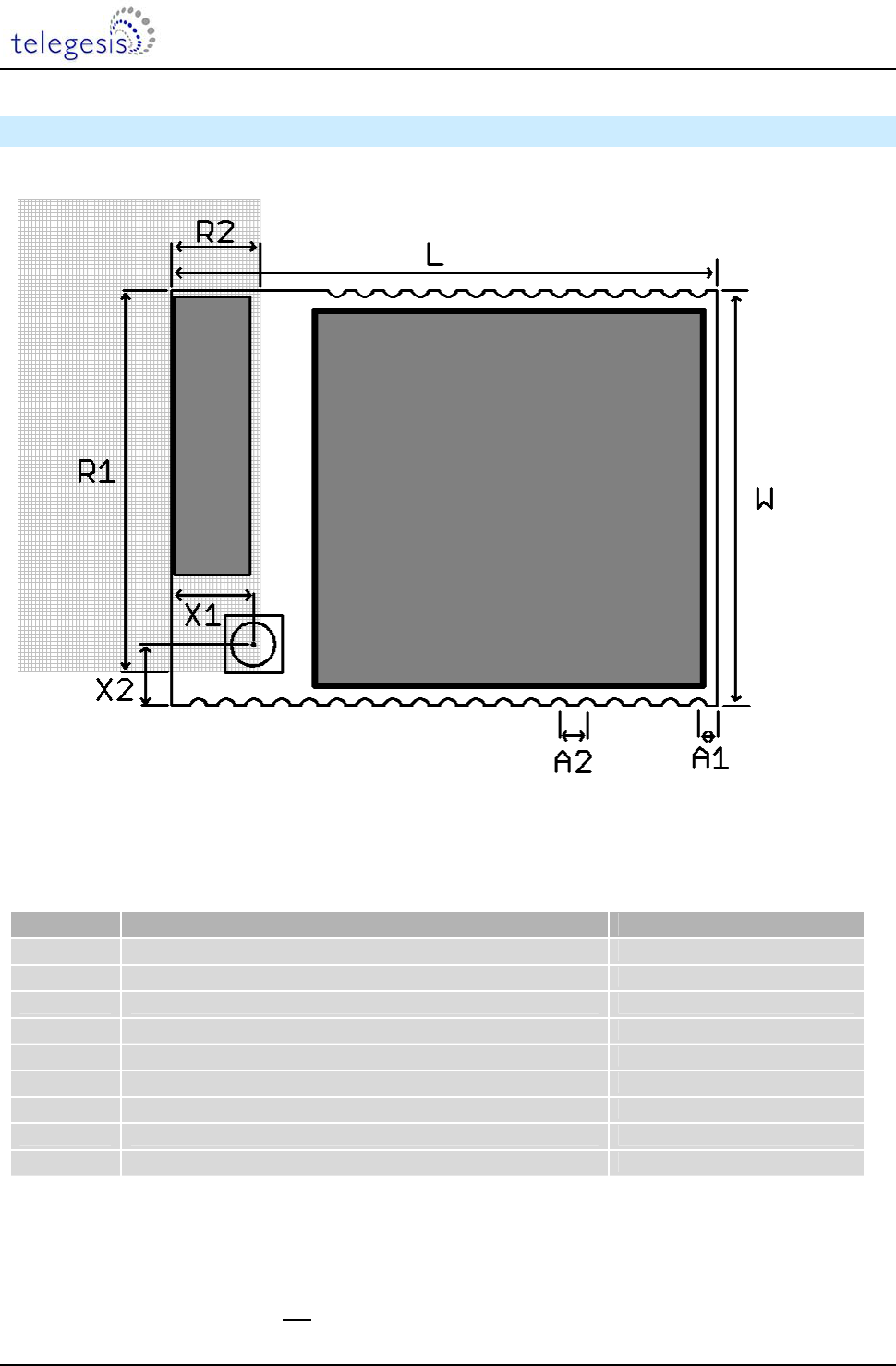
13 Soldering Temperature Time Profile (for reflow soldering)
13.1 For Leaded Solder
Recommended temp. profile
for reflow soldering
Tem
p
.
[
°C
]
Time [s]
235°C max.
220
±
5°C
200°C
150 ±10°C
90 ±30s
10 ±1s
30 +20/-10s
Figure 9. Temperature Profile for Lead Solder
13.2 For Lead-free Solder
Our used temp. profile
for reflow soldering
Temp.[°C]
Time [s]
230°C -250°C max.
220°C
150°C – 190°C
90 ±30s
30 +20/-10s
Figure 10. Temperature Profile for Lead-free Solder
NB:
Maximum Reflow Cycles: 2
Opposite-side reflow is prohibited due to the module’s weight. (i.e. you must not place the
module on the bottom / underside of your pcb and re-flow).
ETRX351-LR AND ETRX357-LR
©2010 Telegesis (UK) Ltd - 21 - ETRX35x-LR Preliminary Product Manual
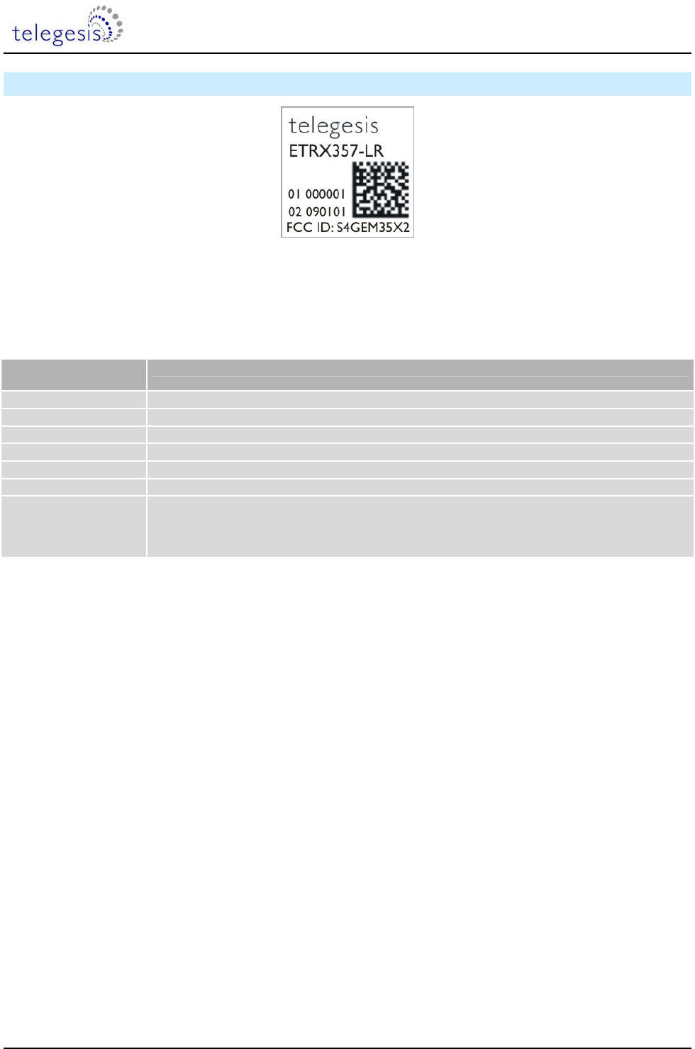
14 Product Label Drawing
Figure 11. Product Label
The label dimensions are 17.0mm x 17.0 mm. The label will withstand temperatures used during
reflow soldering. The characters “HR” are only present on the versions with the Hirose connector,
Imprint Description
ETRX357-LR Module Order code
000001 Indication for the serial number.
090101 Production Date Code in the format YYMMDD, e.g. 090602
01 Indication for batch number
02 Indication for the hardware revision
FCC ID: S4GEM35X2 FCC ID code for this product
2D-Barcode
Information in the Datamatrix 2D-Barcode are the serial number [6 characters], the Part-Order
code [12 characters], identifier for the batch number [2 characters], the identifier for the
hardware release [2 characters] and the production date code in the format Year-Month-Day
[6 characters], separated by a semicolon.
Table 13. ETRX35x-LR Label Details
ETRX351-LR AND ETRX357-LR
©2010 Telegesis (UK) Ltd - 22 - ETRX35x-LR Preliminary Product Manual
15 Recommended Footprint
In order to surface mount a ETRX3 series module, we recommend that you use pads which are
1mm wide and 1.2mm high. You must retain the “keep-out” zone shown in section 12, and ensure
that this area is free of copper tracks and/or copper planes/layers.
You must also ensure that there is no exposed copper on your layout which may contact with the
backside of the ETRX3 series module.
For best RF performance it is required to provide good ground connections to the ground pads of
the module. It is recommended to use multiple vias between each ground pad and a solid ground
plane to minimize inductivity in the ground path.
Figure 12. Recommended Footprint
The land pattern dimensions above serve as a guideline.
We recommend that you use the same pad dimensions for the solder paste screen as you have for
the copper pads. However these sizes and shapes may need to be varied depending on your
soldering processes and your individual production standards. We recommend a paste screen
thickness of 120µm to 150µm.
Although the undersides of the ETRX3 series modules are fully coated, no exposed copper, such
as through-hole vias, planes or tracks on your board component layer, should be located below the
ETRX3 series module in order to avoid ‘shorts’. All ETRX3 series modules use a multilayer PCB
containing an inner RF shielding ground plane, therefore there is no need to have an additional
copper plane directly under the ETRX3 series module.
ETRX351-LR AND ETRX357-LR
©2010 Telegesis (UK) Ltd - 23 - ETRX35x-LR Preliminary Product Manual
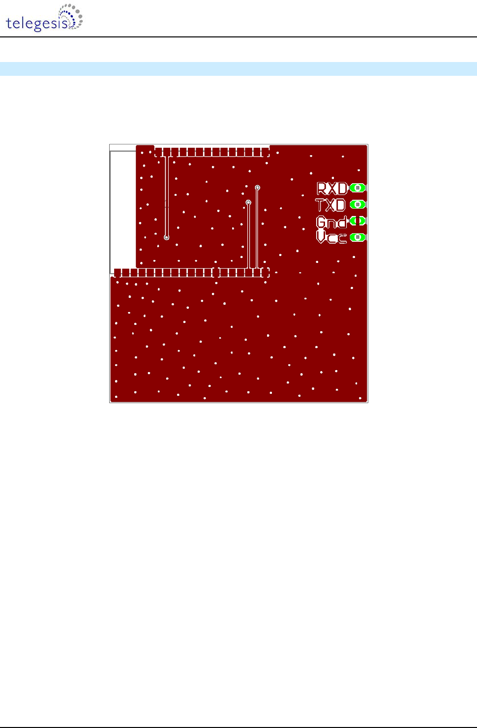
15.1 Example carrier board
Since the RF performance of the module with the on board antenna is strongly dependent on the
proper location of the module on its carrier board, Figure 13 shows the reference carrier board
which was used during testing by Telegesis.
Figure 13. Reference Board
For best performance it is recommended to locate the antenna towards the corner of the carrier
board and to respect the recommended keep-out areas as described in section 12.
Finally to provide a good reference ground to the on board antenna, the carrier board should have
a ground plane spanning no less than 40 x 40mm. In many cases a smaller ground plane will
suffice, but a degradation in radio performance could be the result.

ETRX351-LR AND ETRX357-LR
©2010 Telegesis (UK) Ltd - 24 - ETRX35x-LR Preliminary Product Manual
16 Reliability Tests
The measurements will be conducted after the module has been exposed to standard room
temperature and humidity for 1 hour.
No Item Limit Condition
1 Vibration test Electrical parameter should be
in specification
a) Freq.:10~50Hz,Amplitude:1.5mm
a) 20min. / cycle,1hrs. each of XYZ axis
b) Freq.:30~100Hz, 6G
b) 20min. / cycle,1hrs. each of XYZ axis
2 Shock test the same as the above Dropped onto hard wood from height of
50cm for 3 times
3 Heat cycle test the same as the above -40°C for 30min. and +85°C for 30min.;
each temperature 300 cycles
4 Moisture test the same as the above +60°C, 90% RH, 300h
5 Low temp. test the same as the above -40°C, 300h
6 High temp. test the same as the above +85°C, 300h
Table 14. Reliability Tests
17 Application Notes
17.1 Safety Precautions
These specifications are intended to preserve the quality assurance of products as individual
components.
Before use, check and evaluate their operation when mounted on your products. Abide by
these specifications when using the products. These products may short-circuit. If electrical
shocks, smoke, fire, and/or accidents involving human life are anticipated when a short
circuit occurs, then provide the following failsafe functions as a minimum:
(1) Ensure the safety of the whole system by installing a protection circuit and a protection
device.
(2) Ensure the safety of the whole system by installing a redundant circuit or another
system to prevent a single fault causing an unsafe status.
17.2 Design Engineering Notes
(1) Heat is the major cause of shortening the life of these products. Avoid assembly and
use of the target equipment in conditions where the product’s temperature may exceed
the maximum allowable.
(2) Failure to do so may result in degrading of the product’s functions and damage to the
product.
(3) If pulses or other transient loads (a large load applied in a short time) are applied to the
products, before use, check and evaluate their operation when assembled onto your
products.
(4) These products are not intended for other uses, other than under the special conditions
shown below. Before using these products under such special conditions, check their

ETRX351-LR AND ETRX357-LR
©2010 Telegesis (UK) Ltd - 25 - ETRX35x-LR Preliminary Product Manual
performance and reliability under the said special conditions carefully, to determine
whether or not they can be used in such a manner.
(5) In liquid, such as water, salt water, oil, alkali, or organic solvent, or in places where
liquid may splash.
(6) In direct sunlight, outdoors, or in a dusty environment
(7) In an environment where condensation occurs.
(8) In an environment with a high concentration of harmful gas (e.g. salty air, HCl, Cl2,
SO2, H2S, NH3, and NOx)
(9) If an abnormal voltage is applied due to a problem occurring in other components or
circuits, replace these products with new products because they may not be able to
provide normal performance even if their electronic characteristics and appearances
appear satisfactory.
(10) Mechanical stress during assembly of the board and operation has to be avoided.
(11) Pressing on parts of the metal cover or fastening objects to the metal cover is not
permitted.
17.3 Storage Conditions
(1) The module must not be stressed mechanically during storage.
(2) Do not store these products in the following conditions or the performance
characteristics of the product, such as RF performance, may well be adversely
affected:
(3) Storage in salty air or in an environment with a high concentration of corrosive gas,
such as Cl2, H2S, NH3, SO2, or NOX
(4) Storage in direct sunlight
(5) Storage in an environment where the temperature may be outside the range of 5°C to
35°C range, or where the humidity may be outside the 45 to 85% range.
(6) Storage (before assembly of the end product) of the modules for more than one year
after the date of delivery at your company even if all the above conditions (1) to (3)
have been met, should be avoided.
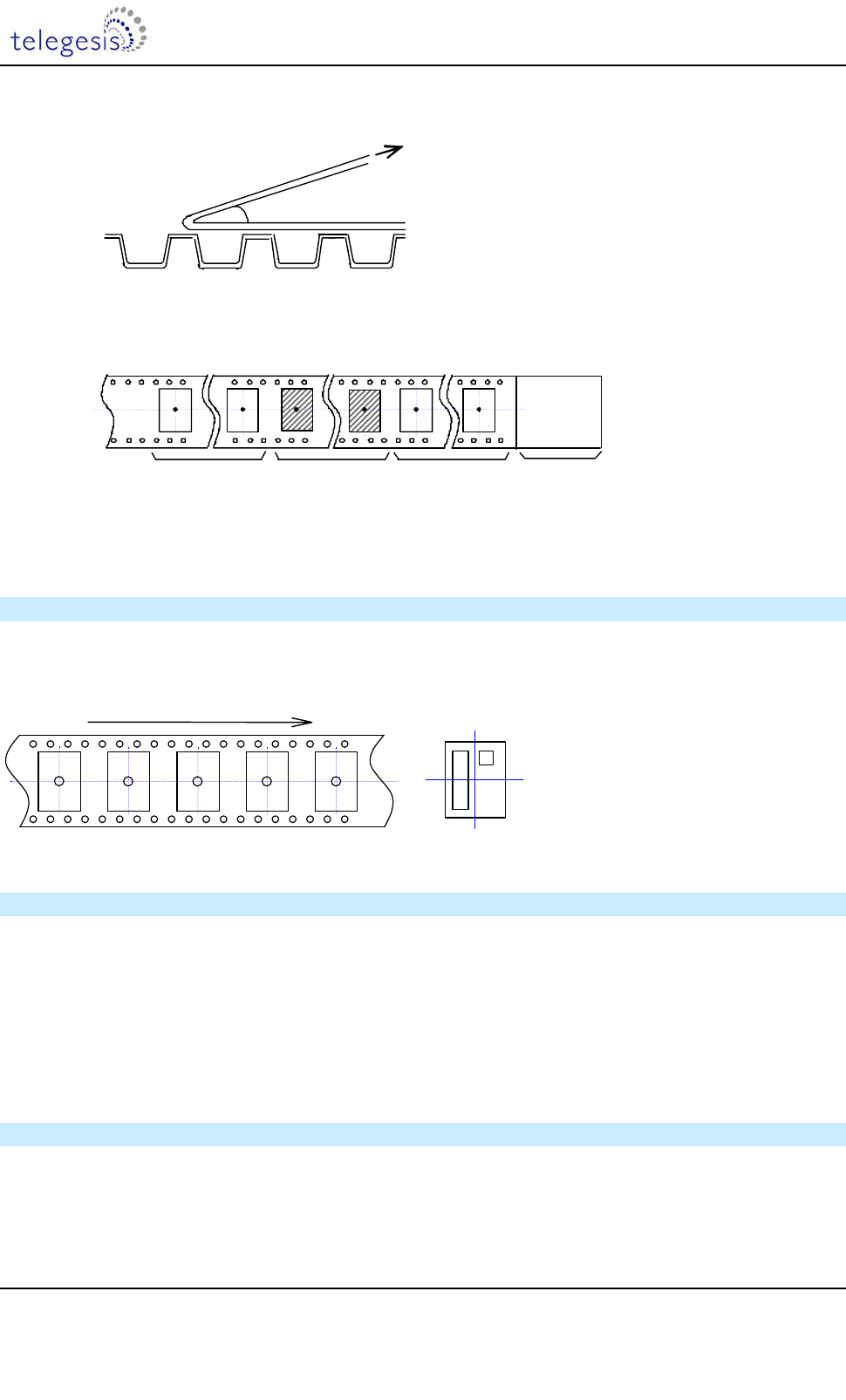
18 Packaging
18.1 Embossed Tape
(1) Dimension of the tape
t.b.d.
ETRX351-LR AND ETRX357-LR
©2010 Telegesis (UK) Ltd - 26 - ETRX35x-LR Preliminary Product Manual
(2) Cover tape peel force
Force direction
Speed = 300mm/min.
Cover tape peel force
=0.098~0.68N ( 10~70g)
= 10deg
(3) Empty pockets
Empty pockets
Components
Empty pockets Top cover
Direction of
g
NB: Empty pockets in the component packed area will be less than two per reel and those empty
pockets will not be consecutive.
18.2 Component Orientation
Top cover tape will not obstruct the carrier tape holes and will not extend beyond the edges of the
carrier tape
(top view)
Component Orientation
Part No.
Direction
18.3 Reel Dimensions
(4) Quantity per reel: 400 pieces
(5) Marking: Part No. / Quantity / Lot No. and manufacturer part# with bar-code will be on
the reel
t.b.d.
18.4 Packaging
(6) Each reel will be packed in a hermetically-sealed bag
(7) Marking : Part No. / Quantity / Lot No. and manufacturer part# with bar-code

ETRX351-LR AND ETRX357-LR
©2010 Telegesis (UK) Ltd - 27 - ETRX35x-LR Preliminary Product Manual
19 Ordering Information
Ordering/Product Code Description
ETRX351-LR
ETRX357-LR
Telegesis Long Range ZigBee Module with Ember ZigBee®
Technology:
• Based on Ember EM351 or EM357
• Telegesis AT Style Command Interpreter and
• EmberZNet3.xx meshing and self-healing ZigBee PRO
stack
• Integrated 2.4GHz Antenna
ETRX3DVK Telegesis Development Kit with:
• 3 x USB Development Boards
• 3 x USB Cable
• 2 x ETRX35x on Carrier-Board
• 2 x ETRX35xHR on Carrier-Board
• 2 x ETRX35x-LR on Carrier-Board
• 2 x ETRX35xHR-LR on Carrier-Board
• 1 x ETRX2USB stick
• 2 x Large Antenna
• 2 x Small Stubby Antenna
Notes:
• Customers’ PO’s must state the Ordering/Product Code.
• There is no “blank” version of the ETRX35x-LR modules available. All Modules are pre-
programmed with the Telegesis AT style command interpreter based on the EmberZNet
stack. (Where customers wish to add their own firmware they can erase and write it to the
flash memory of the EM35x).

ETRX351-LR AND ETRX357-LR
©2010 Telegesis (UK) Ltd - 28 - ETRX35x-LR Preliminary Product Manual
20 Trademarks
All trademarks, registered trademarks and products names are the sole property of their respective
owners.
21 Disclaimer
Product and company names and logos referenced may either be trademarks or registered
trademarks of their respective companies. We reserve the right to make modifications and/or
improvements without prior notification. All information is correct at time of issue. Telegesis (UK)
Ltd does not convey any license under its patent rights or assume any responsibility for the use of
the described product
22 RoHS Declaration
Declaration of environmental compatibility for supplied products:
Hereby we declare to our best present knowledge based on the declaration of our suppliers that
this product does not contain the following substances which are banned by Directive 2002/95/EC
(RoHS) or if they do, contain a maximum concentration of 0,1% by weight in homogeneous
materials for:
• Lead and lead compounds
• Mercury and mercury compounds
• Chromium (VI)
• PBB (polybrominated biphenyl) category
• PBDE (polybrominated biphenyl ether) category
And a maximum concentration of 0.01% by weight in homogeneous materials for:
• Cadmium and cadmium compounds
23 Data Sheet Status
Telegesis (UK) Ltd. reserves the right to change the specification without notice, in order to
improve the design and supply the best possible product. Please consult the most recently issued
data sheet before initiating or completing a design.
24 Life Support Policy
This product is not designed for use in life support appliances, devices, or systems where
malfunction can reasonably be expected to result in a significant personal injury to the user, or as a
critical component in any life support device or system whose failure to perform can be reasonably
expected to cause the failure of the life support device or system, or to affect its safety or
effectiveness. Customers using or selling these products for use in such applications do so at their
own risk and agree to fully indemnify Telegesis (UK) Ltd. for any damages resulting.

ETRX351-LR AND ETRX357-LR
©2010 Telegesis (UK) Ltd - 29 - ETRX35x-LR Preliminary Product Manual
25 Related Documents
[1] IEEE Standard 802.15.4 –2003 Wireless Medium Access Control (MAC) and Physical
Layer (PHY) Specifications for Low-Rate Wireless Personal Area Networks (LR-
WPANs)
[2] Datasheet EM35x, Ember. (www.ember.com)
[3] Datasheet U.FL-Series 2004.2 Hirose Ultra Small Surface Mount Coaxial Connectors -
Low Profile 1.9mm or 2.4mm Mated Height
[4] The ZigBee® specification (www.zigbee.org)
[5] Specification for Antenova Rufa Antenna (www.antenova.com)
26 Contact Information
Website: www.telegesis.com
E-mail sales@telegesis.com
Telegesis (UK) Limited
Abbey Barn Business Centre
Abbey Barn Lane
High Wycombe
Bucks
HP10 9QQ
UK
Tel: +44 (0)1494 510199
Fax: +44 (0)5603 436999