Silicon Laboratories Finland WT32AE Bluetooth Audio Module User Manual WT32 Datasheet Preliminary
Silicon Laboratories Finland Oy Bluetooth Audio Module WT32 Datasheet Preliminary
Contents
- 1. User Manual
- 2. FCC Audio single
- 3. VH_Audio_Handbook_EN
User Manual
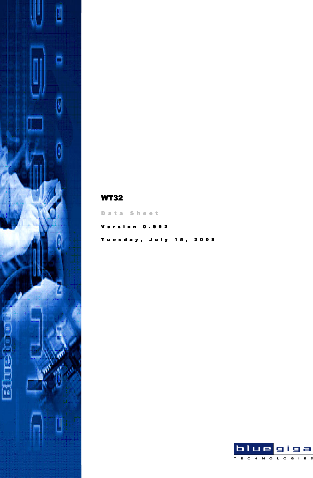
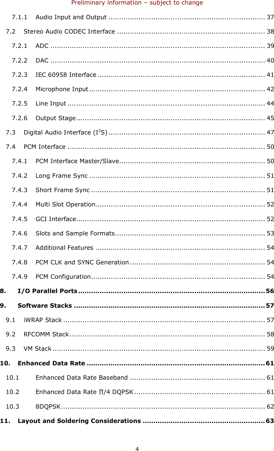
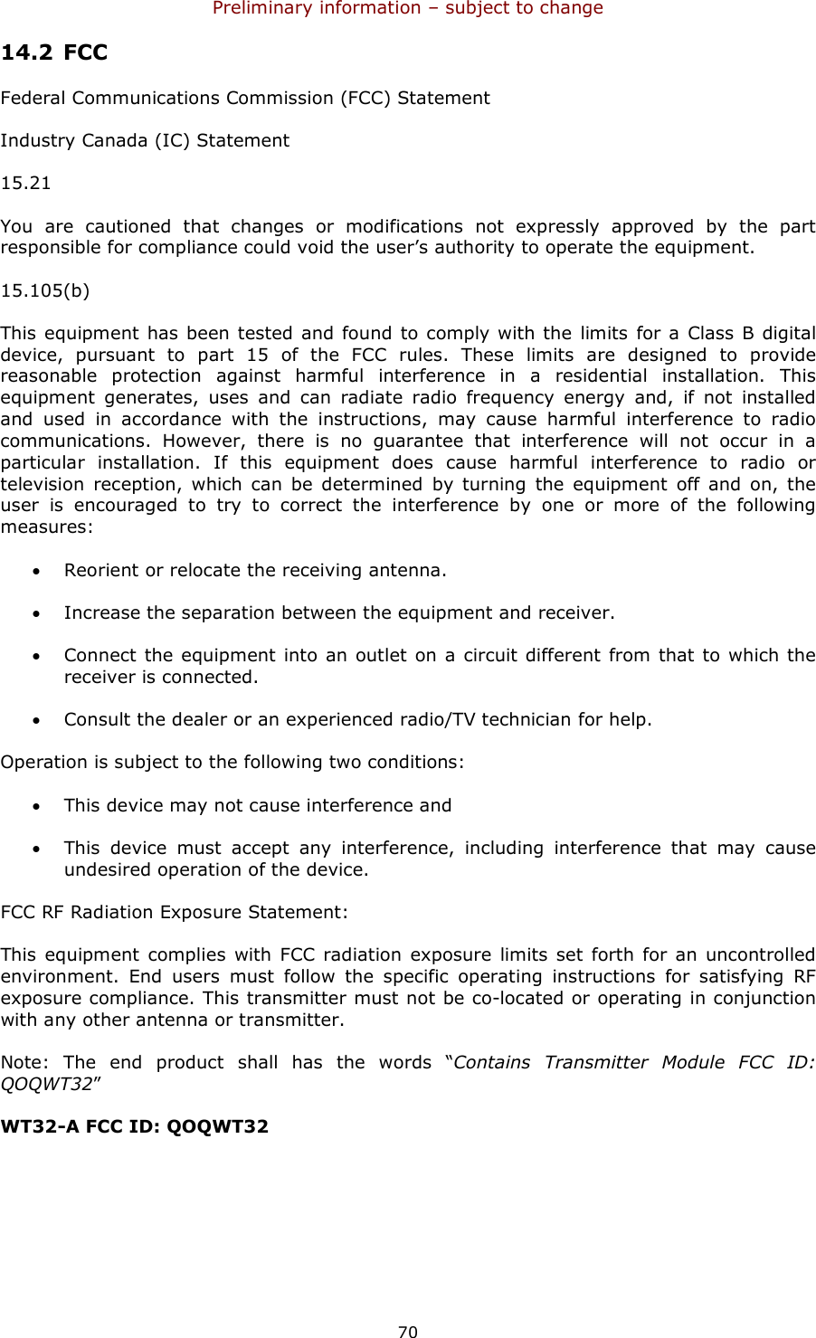
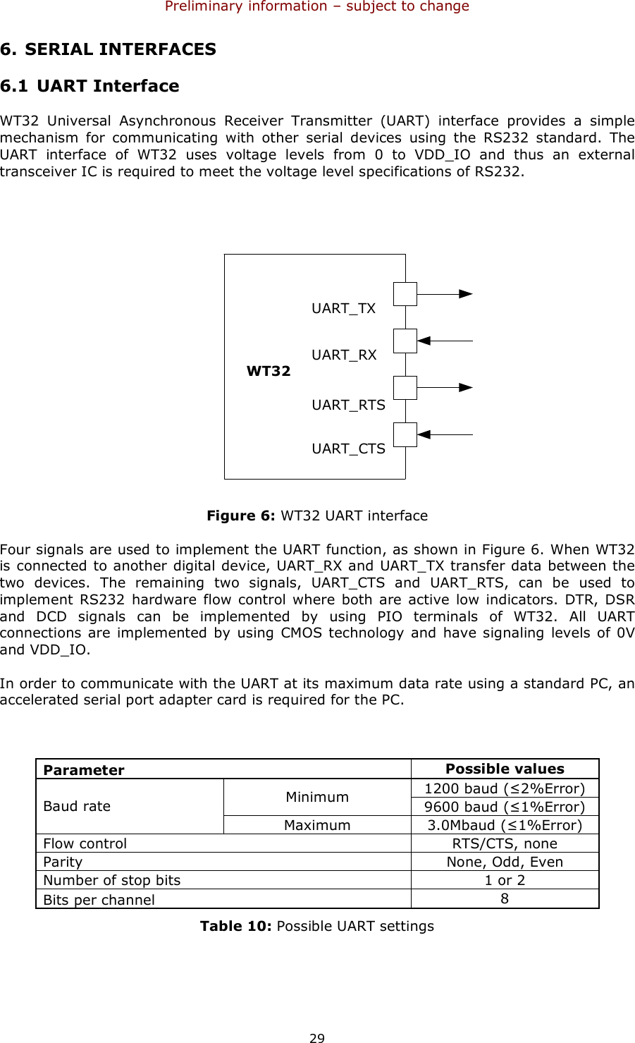
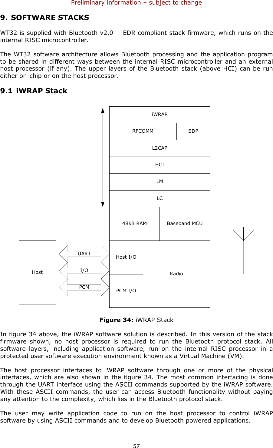
![Preliminary information – subject to change 28 The chip status after a reset is as follows: • Warm Reset: data rate and RAM data remain available • Cold Reset(10): data rate and RAM data are not available Table 8 shows the pin states of WT32 on reset. Pull-up (PU) and pull-down (PD) default to weak values unless specified otherwise. Pin Name / Group I/O Type State on Reset USB_D+ Digital bi-directional N/A USB_D- Digital bi-directional N/A UART_RX Digital input with PD PD UART_CTS Digital input with PD PD UART_TX Digital bi-directional with PU PU UART_RTS Digital bi-directional with PU PU SPI_MOSI Digital input with PD PD SPI_CLK Digital input with PD PD SPI_CS# Digital input with PU PU SPI_MISO Digital tri-state output with PD PD PCM_IN Digital input with PD PD PCM_CLK Digital bi-directional with PD PD PCM_SYNC Digital bi-directional with PD PD PCM_OUT Digital tri-state output with PD PD PIO[10:0] Digital bi-directional with PU/PD PD Table 9: Pin states on reset](https://usermanual.wiki/Silicon-Laboratories-Finland/WT32AE.User-Manual/User-Guide-976248-Page-29.png)
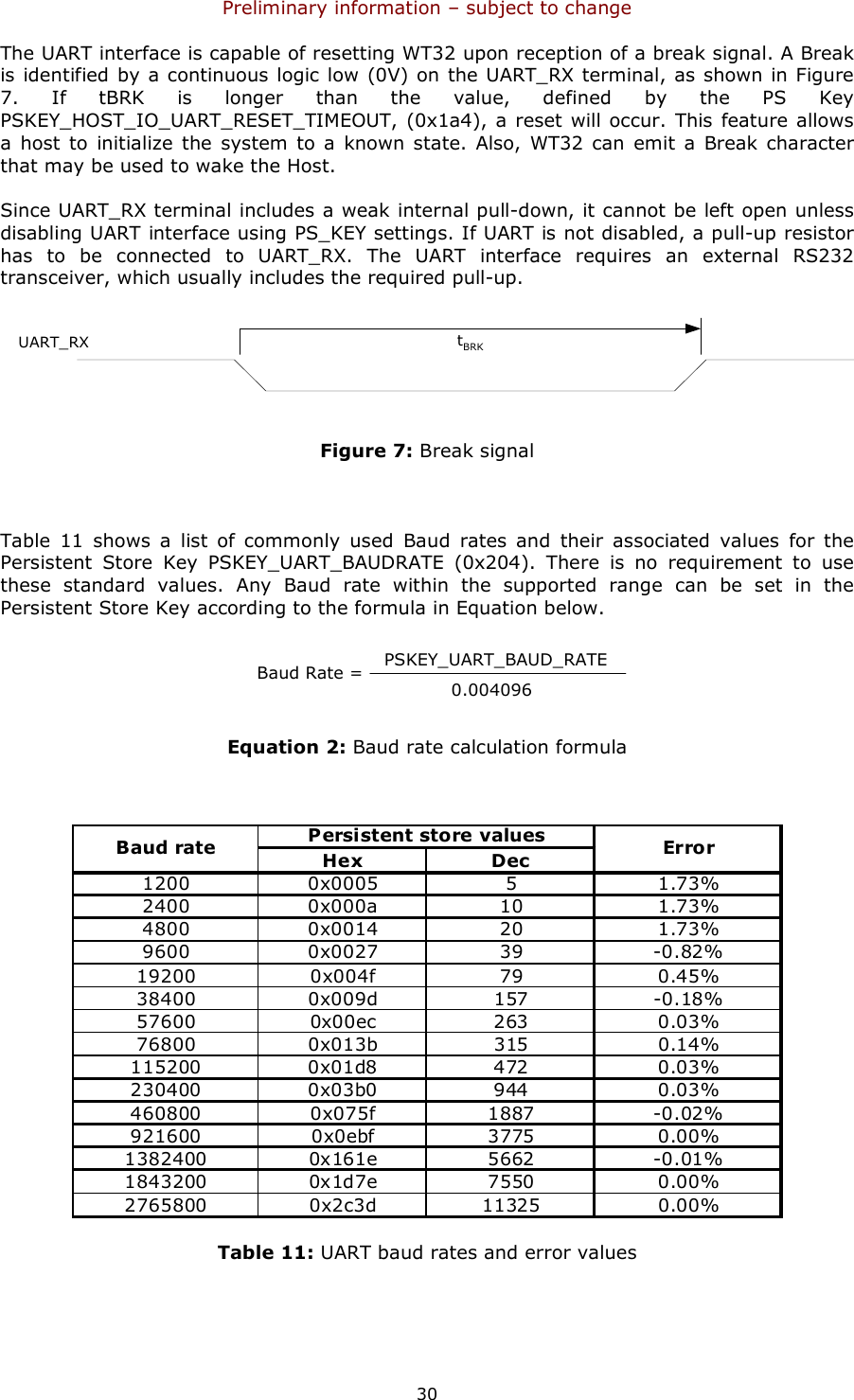
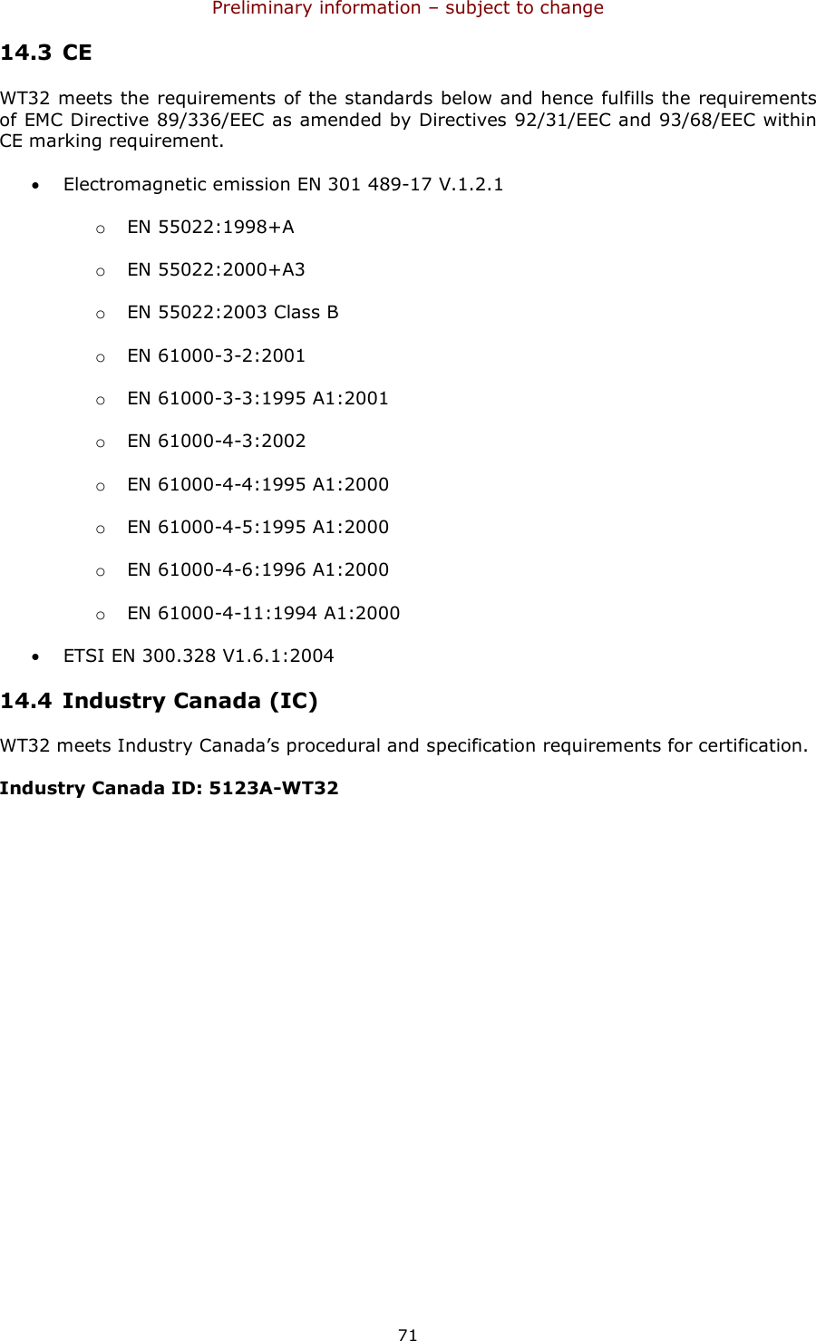
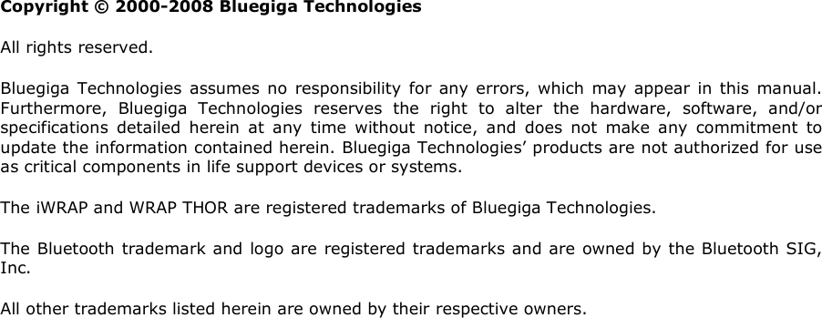
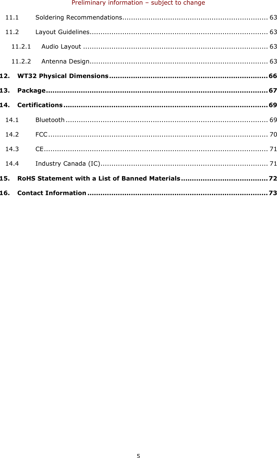
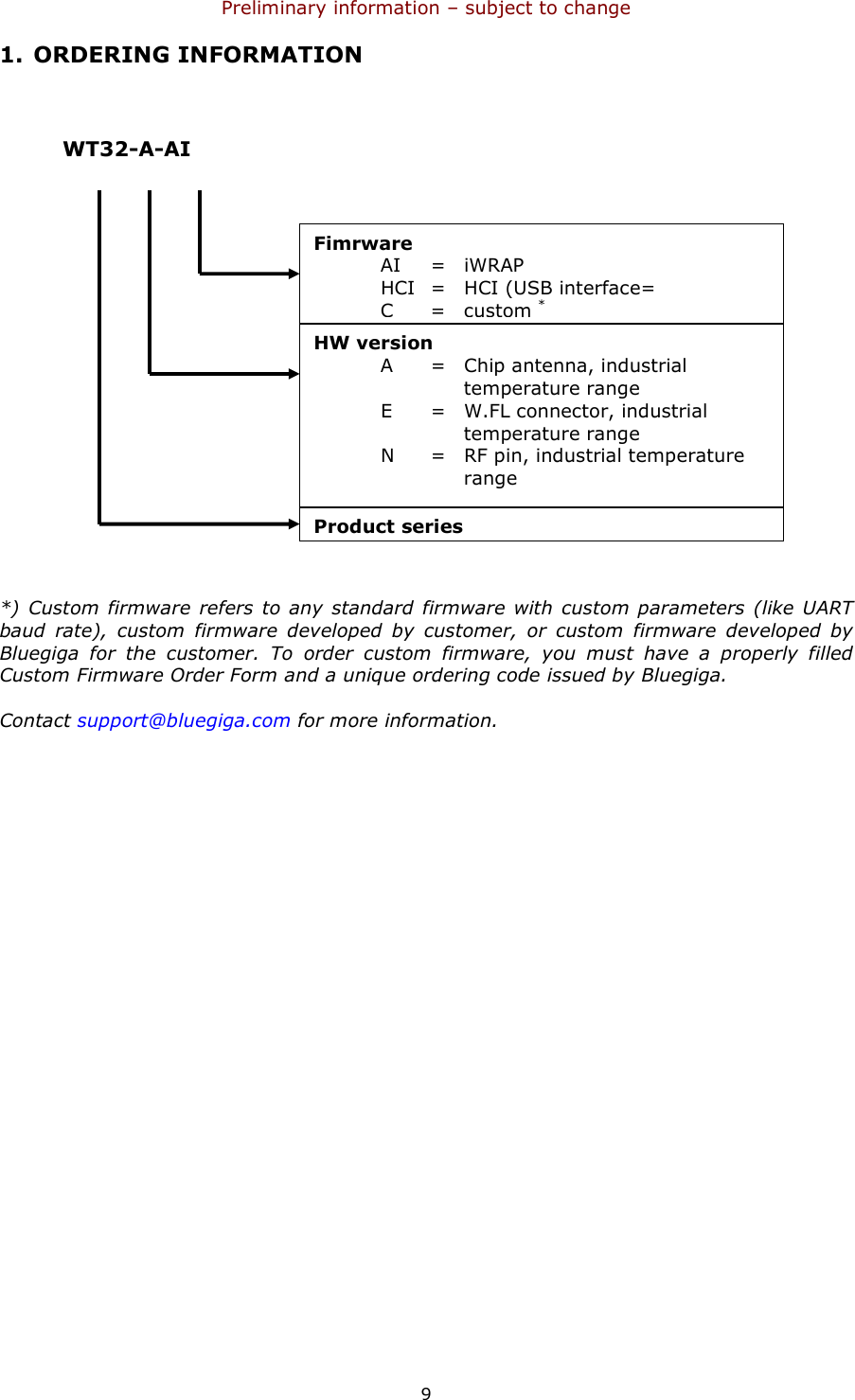
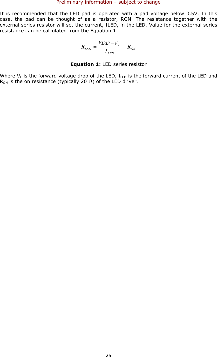
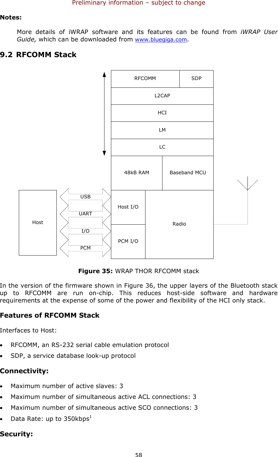
![Preliminary information – subject to change 31 6.1.1 UART Configuration While RESET is Active The UART interface for WT32 while the chip is being held in reset is tri-state. This will allow the user to daisy chain devices onto the physical UART bus. The constraint on this method is that any devices connected to this bus must tri-state when a WT32 reset is de-asserted and the firmware begins to run. 6.1.2 UART Bypass Mode Alternatively, for devices that do not tri-state the UART bus, the UART bypass mode on WT32 can be used. The default state of WT32 after reset is de-asserted, this is for the host UART bus to be connected to the WT32 UART, thereby allowing communication to WT32 via the UART. In order to apply the UART bypass mode, a BCCMD command will be issued to WT32. Upon this, WT32 will switch the bypass to PIO[7:4] as shown in Figure 8. Once the bypass mode has been invoked, WT32 will enter the deep sleep state indefinitely. In order to re-establish communication with WT32, the chip must be reset so that the default configuration takes effect. It is important for the host to ensure a clean Bluetooth disconnection of any active links before the bypass mode is invoked. Therefore, it is not possible to have active Bluetooth links while operating the bypass mode. The current consumption for a device in UART Bypass Mode is equal to the values quoted for a device in standby mode. WT12HostprocessorTestinterfaceRXDCTSRTSTXDAnotherdeviceTXRTSCTSRXUART_TXUART_RTSUART_CTSUART_RXRESETPIO5PIO6PIO7PIO4UARTWTxx Figure 8: UART bypass mode](https://usermanual.wiki/Silicon-Laboratories-Finland/WT32AE.User-Manual/User-Guide-976248-Page-32.png)
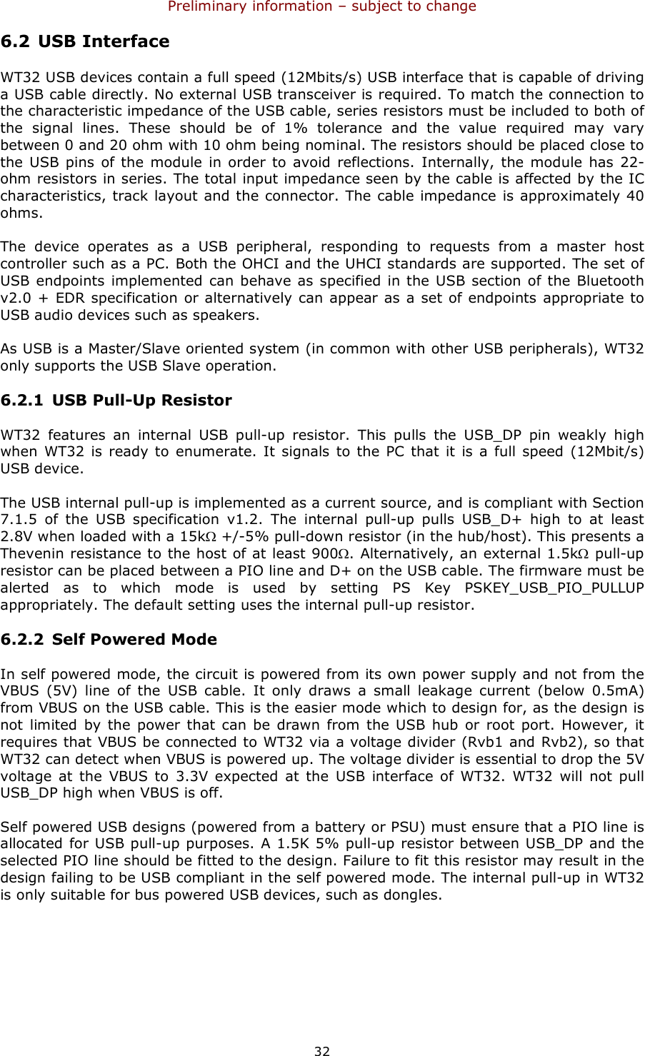
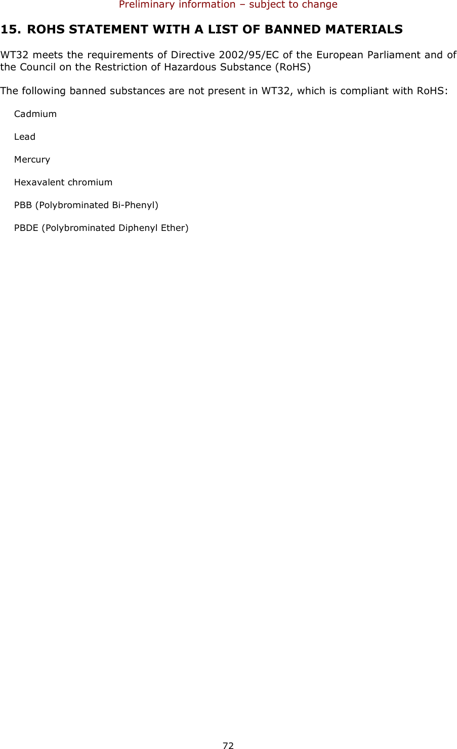
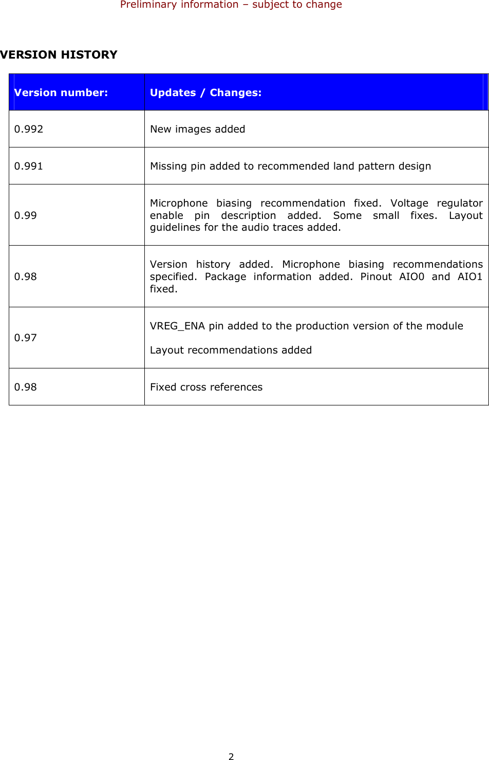
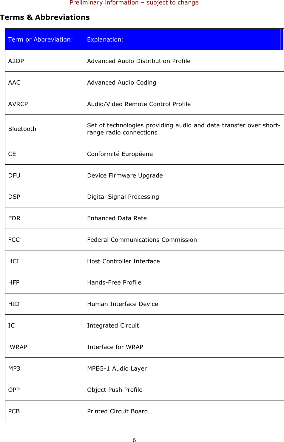
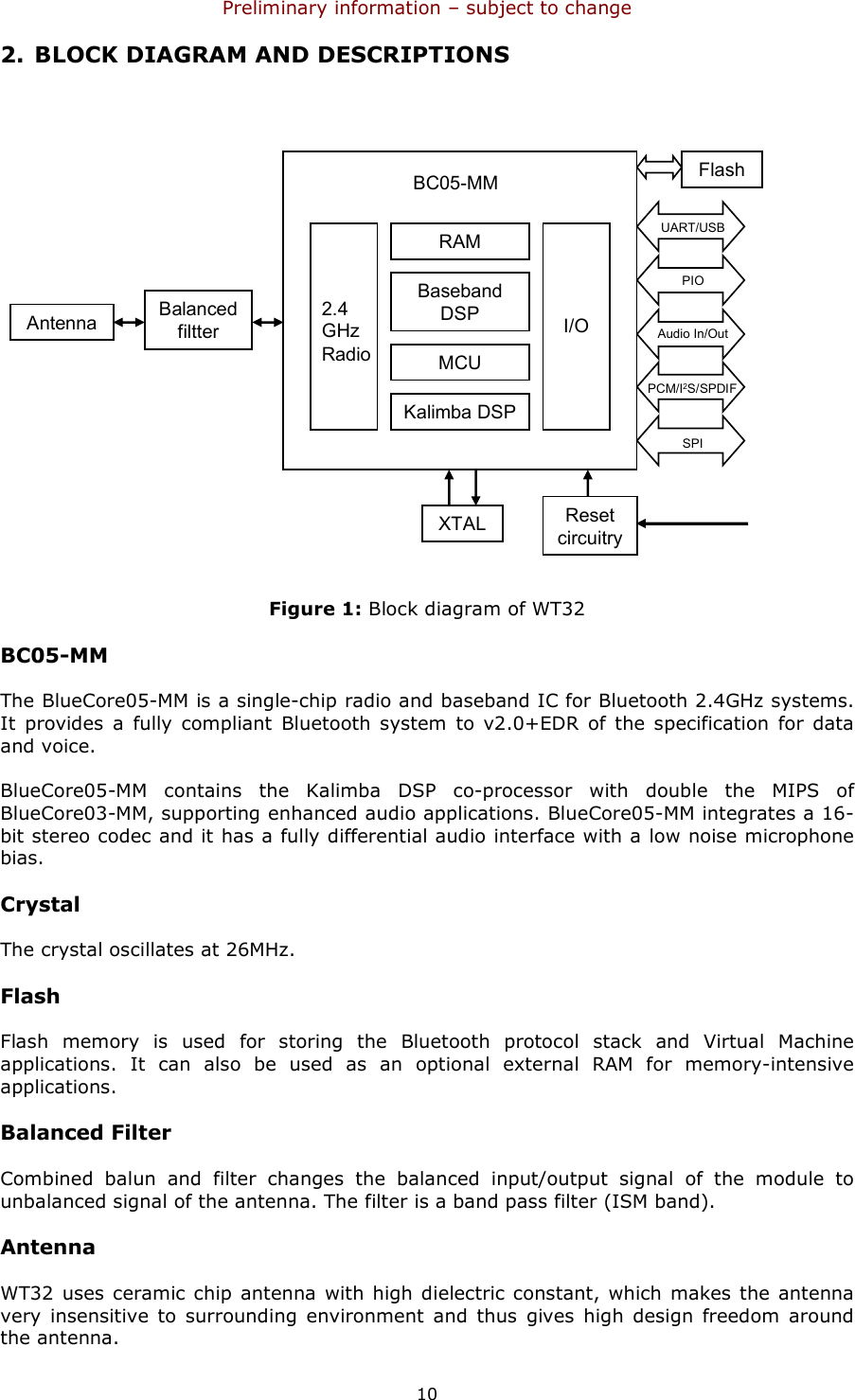
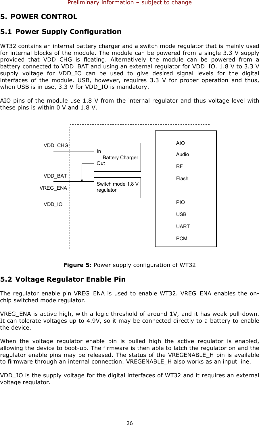
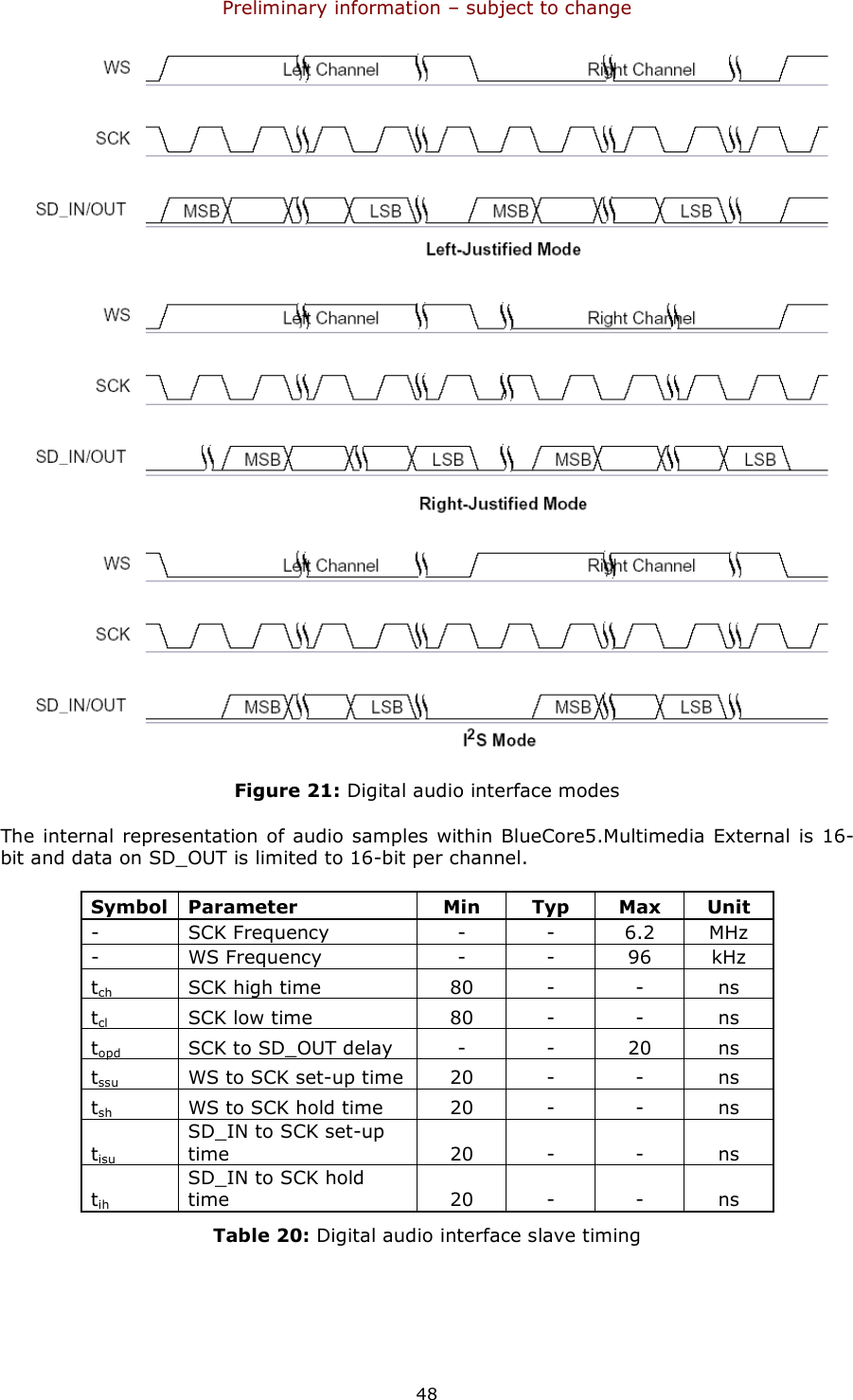
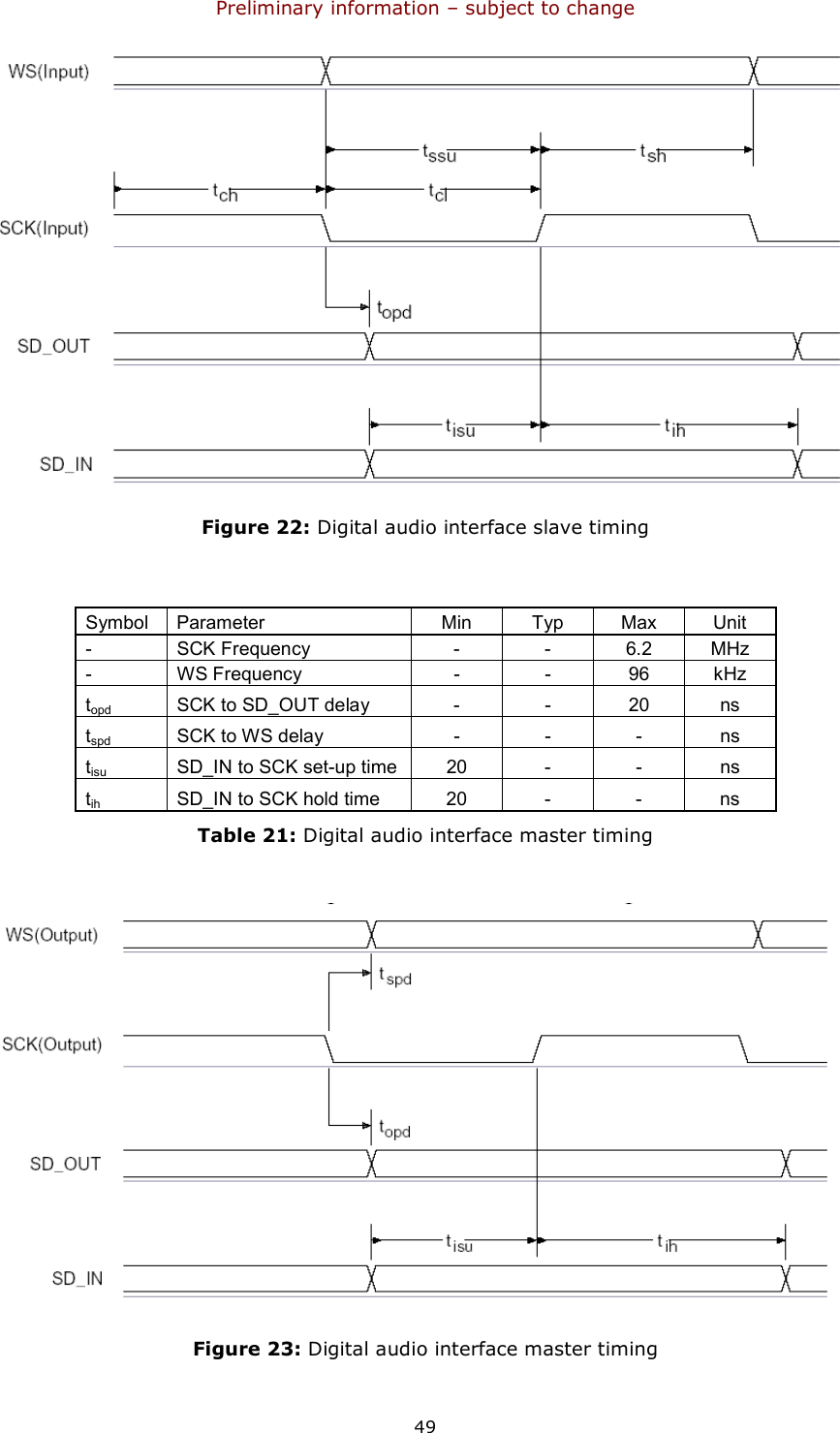
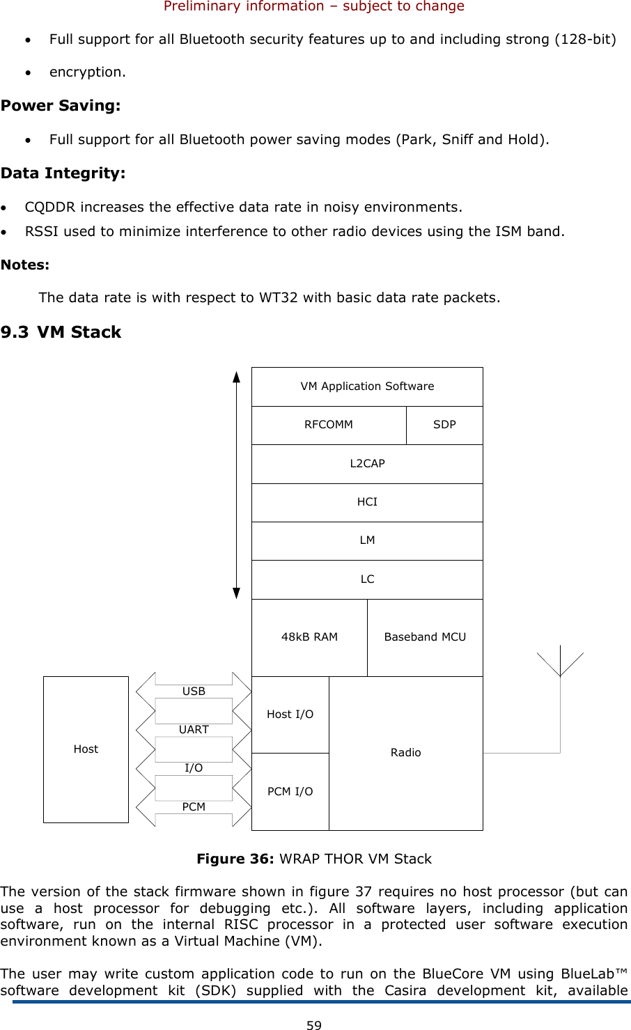
![Preliminary information – subject to change 47 7.3 Digital Audio Interface (I2S) The digital audio interface supports the industry standard formats for I2S, left-justified (LJ) or right-justified(RJ). The interface shares the same pins as the PCM interface, which means that each audio bus is mutually exclusive in its usage. Table 18 lists these alternative functions. Figure 21 shows the timing diagram. PCM Interface I2S Interface PCM_OUT SD_OUT PCM_IN SD_IN PCM_SYNC WS PCM_CLK SCK Table 18: Alternative Functions of the Digital Audio Bus Interface on the PCM Interface Table 19 describes the values for the PS Key (PSKEY_DIGITAL_AUDIO_CONFIG) that is used to set-up the digital audio interface. For example, to configure an I2S interface with 16-bit SD data set PSKEY_DIGITAL_CONFIG to 0x0406. Bit Mask Name Description D[0] 0x0001 CONFIG_JUSTIFY_FORMAT 0 for left justified, 1 for right justified D[1] 0x0002 CONFIG_LEFT_JUSTIFY_DELAY For left justified formats: 0 is MSB of SD data occurs in the first SCLK period following WS transition. 1 is MSB of SD data occurs in the second SCLK period. D[2] 0x0004 CONFIG_CHANNEL_POLARITY For 0, SD data is left channel when WS is high. For 1 SD data is right channel. D[3] 0x0008 CONFIG_AUDIO_ATTEN_EN For 0, 17 bit SD data is rounded down to 16 bits. For 1, the audio attenuation defined in CONFIG_AUDIO_ATTEN is applied over 24 bits with saturated rounding. Requires CONFIG_16_BIT_CROP_EN to be 0. D[7:4] 0x00F0 CONFIG_AUDIO_ATTEN Attenuation in 6 dB steps. D[9:8] 0x0300 CONFIG_JUSTIFY_RESOLUTION Resolution of data on SD_IN, 00=16 bit, 01=20 bit, 10=24 bit, 11=Reserved. This is required for right justified format and with left justified LSB first. D[10] 0x0400 CONFIG_16_BIT_CROP_EN For 0, 17 bit SD_IN data is rounded down to 16 bits. For 1 only the most significant 16 bits of data are received. Table 19: PSKEY_DIGITAL_AUDIO_CONFIG](https://usermanual.wiki/Silicon-Laboratories-Finland/WT32AE.User-Manual/User-Guide-976248-Page-48.png)
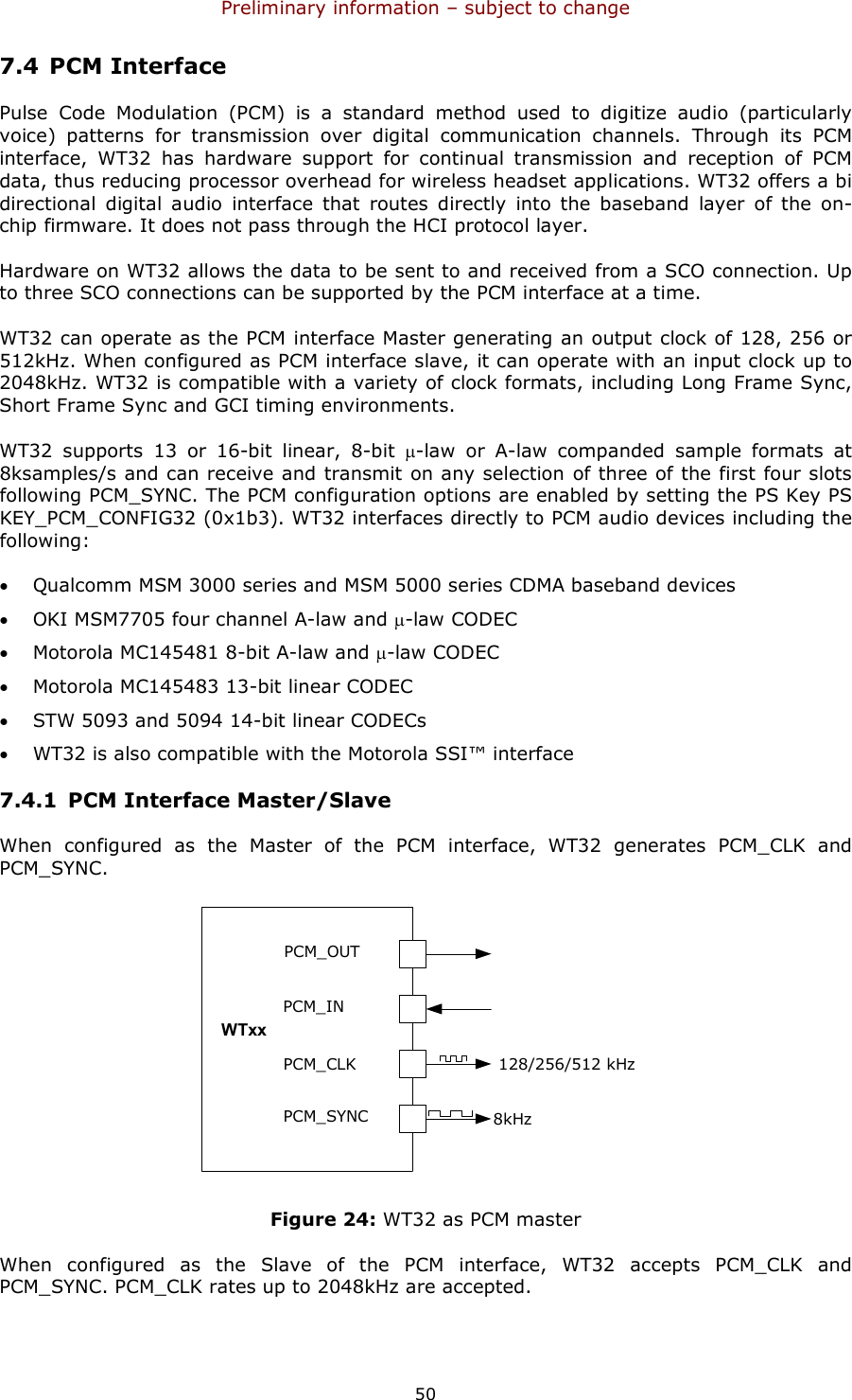
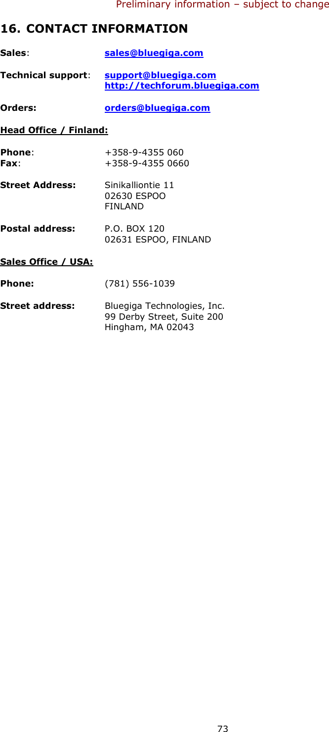
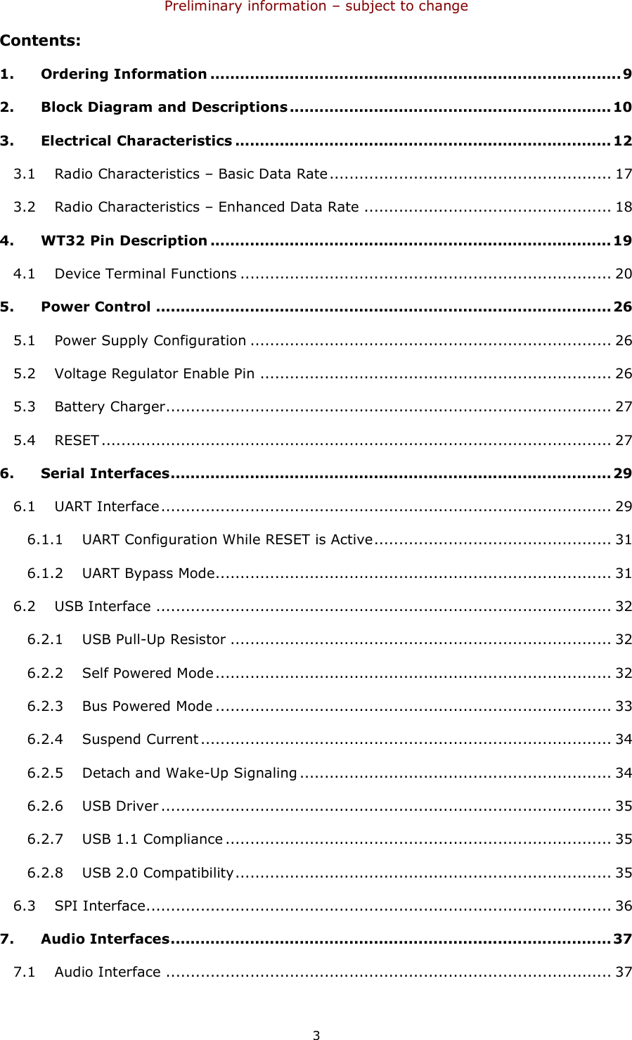
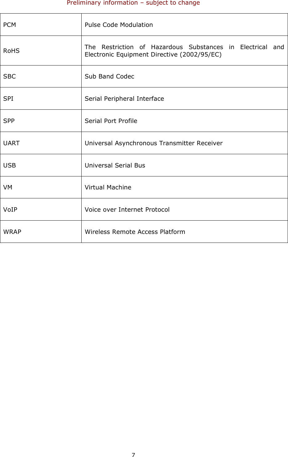
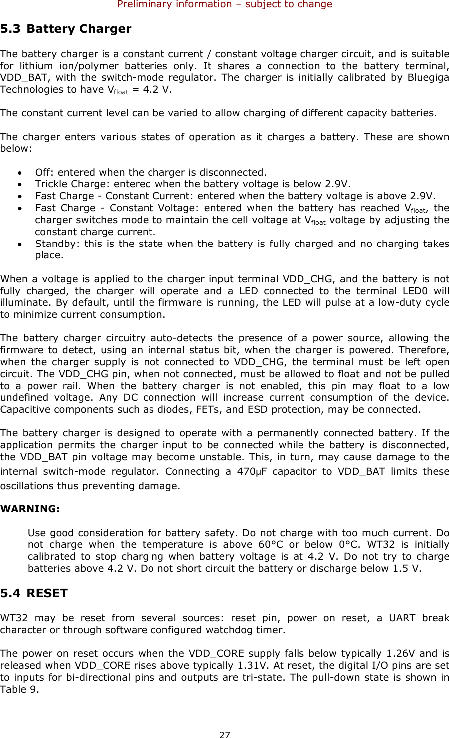
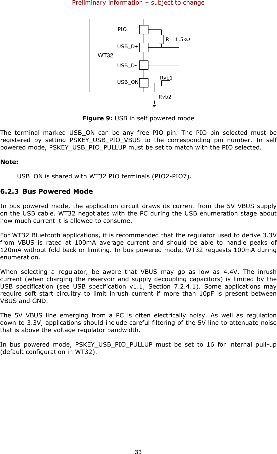
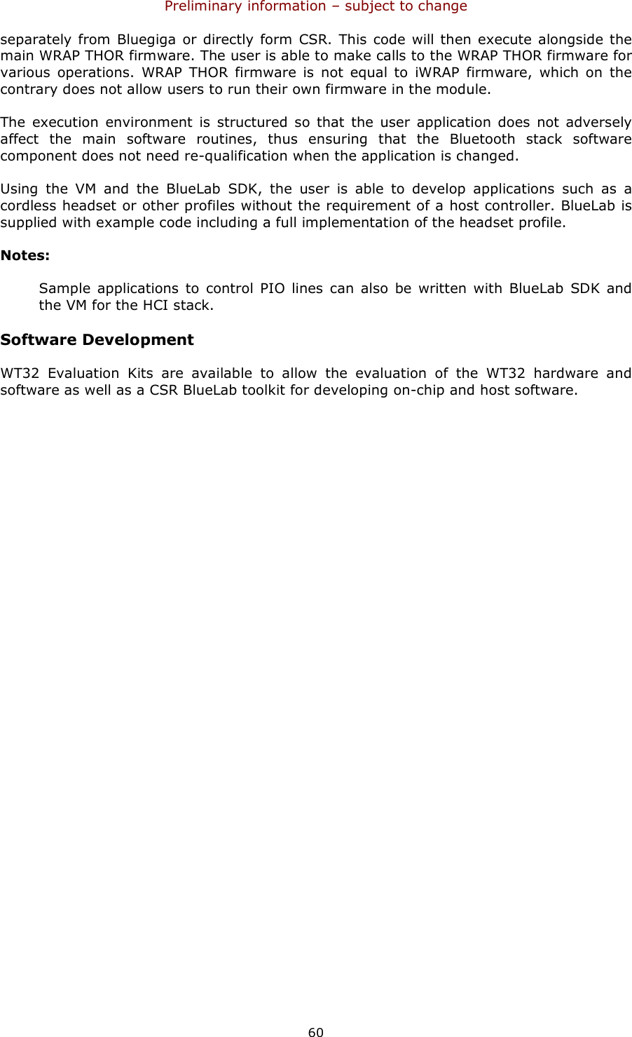
![Preliminary information – subject to change 55 Name Bit position Description- 0 Set to 0SLAVE MODE EN 10 selects Master mode with internal generation of PCM_CLK and PCM_SYNC. 1 selects Slave mode requiring externally generated PCM_CLK and PCM_SYNC. This should be set to 1 if 48M_PCM_CLK_GEN_EN (bit 11) is set.SHORT SYNC EN 2 0 selects long frame sync (rising edge indicates start of frame), 1 selects short frame sync (falling edge indicates start of frame).- 3 Set to 0SIGN EXTENDED EN 40 selects padding of 8 or 13-bit voice sample into a 16- bit slot by inserting extra LSBs, 1 selects sign extension. When padding is selected with 3-bit voice sample, the 3 padding bits are the audio gain setting; with 8-bit samples the 8 padding bits are zeroes.LSB FIRST EN 5 0 transmits and receives voice samples MSB first, 1 uses LSB first.TX TRISTATE EN 60 drives PCM_OUT continuously, 1 tri-states PCM_OUT immediately after the falling edge of PCM_CLK in the last bit of an active slot, assuming the next slot is not active.TX TRISTATE RISING EDGE EN 70 tristates PCM_OUT immediately after the falling edge of PCM_CLK in the last bit of an active slot, assuming the next slot is also not active. 1 tristates PCM_OUT after the rising edge of PCM_CLK.SYNC SUPPRESS EN 80 enables PCM_SYNC output when master, 1 suppresses PCM_SYNC whilst keeping PCM_CLK running. Some CODECS utilize this to enter a low power state.GCI MODE EN 9 1 enables GCI mode.MUTE EN 10 1 forces PCM_OU T to 0.48M PCM CLK GEN EN 110 sets PCM_CLK and PCM_SYNC generation via DDS from internal 4 MHz clock, as for BlueCore4-External. 1 sets PCM_CLK and PCM_SYNC generation via DDS from internal 48 MHz clock.LONG LENGTH SYNC EN 120 sets PCM_SYNC length to 8 PCM_CLK cycles and 1 sets length to 16 PCM_CLK cycles. Only applies for long frame sync and with 48M_PCM_CLK_GEN_EN set to 1.- [20:16] Set to 0b00000.MASTER CLK RATE [22:21] Selects 128 (0b01), 256 (0b00), 512 (0b10) kHz PCM_CLK frequency when master and 48M_PCM_CLK_GEN_EN (bit 11) is low. Table 22: PSKEY_PCM_CONFIG32 description NameBit positionDescriptionCNT LIMIT[12:0]Sets PCM_CLK counter limitCNT RATE[23:16]Sets PCM_CLK count rate.SYNC LIMIT [31:24] Sets PCM_SYNC division relative to PCM_CLK. Table 23: PSKEY_PCM_LOW_JITTER_CONFIG Description](https://usermanual.wiki/Silicon-Laboratories-Finland/WT32AE.User-Manual/User-Guide-976248-Page-56.png)
![Preliminary information – subject to change 56 8. I/O PARALLEL PORTS The Parallel Input Output (PIO) Port is a general-purpose I/O interface to WT32. The port consists of eleven programmable, bi-directional I/O lines, PIO[10:0]. Programmable I/O lines can be accessed either through an embedded application running on WT32 or through private channel or manufacturer-specific HCI commands. All PIO lines are configured as inputs with weak pull downs at reset. PIO[2] / USB_PULL_UP (1) The function depends on whether WT32 is a USB or UART capable version. On UART versions, this terminal is a programmable I/O. On USB versions, it can drive a pull-up resistor on USB_D+. For applications using external RAM, this terminal may be programmed for chip select. PIO[3] / USB_WAKE_UP (1) On UART versions of WT32, this terminal is a programmable I/O. On USB versions, its function is selected by setting the Persistent Store Key PSKEY_USB_PIO_WAKEUP (0x2cf) either as a programmable I/O or as a USB_WAKE_UP function. PIO[4] / USB_ON (1) On UART versions of WT32, this terminal is a programmable I/O. On USB versions, the USB_ON function is also selectable. PIO[5] / USB_DETACH (1) On UART versions of WT32, this terminal is a programmable I/O. On USB versions, the USB_DETACH function is also selectable. PIO[6] / CLK_REQ Function is determined by Persistent Store Keys. Using PSKEY_CLOCK_REQUEST_ENABLE, (0x246) this terminal can be configured to be low when WT32 is in deep sleep and high when a clock is required. The clock must be supplied within 4ms of the rising edge of PIO[6] to avoid losing timing accuracy in certain Bluetooth operating modes. PIO[7] Programmable I/O terminal. PIO[8] Programmable I/O terminal. PIO[9] Programmable I/O terminal. PIO[10] Programmable I/O terminal.](https://usermanual.wiki/Silicon-Laboratories-Finland/WT32AE.User-Manual/User-Guide-976248-Page-57.png)
![Preliminary information – subject to change 69 14. CERTIFICATIONS WT32 is compliant to the following specifications. 14.1 Bluetooth WT32 module is Bluetooth qualified and listed as Controller Subsystem. When WT32 is combined with a Bluetooth upper layer stack listed as Host Subsystem, such as Bluegiga Technologies’ iWRAP, WT32 forms a full Bluetooth end-device which can be listed as End Product for free. If not modified in any way, it is a complete Bluetooth entity, containing software and hardware functionality as well as the whole RF-part including the antenna. If changes are made in the parameter set, added profiles or in the antenna design, it is required to be submitted to a BQB (Bluetooth Qualification Body) for evaluation on what needs to be tested. With HCI firmware WT32 will not meet the requirements of end product qualification. WT32 is Bluetooth compliant to the following specifications RF as defined in Part A of the Bluetooth specification v2.1+EDR, Vol.2 Core System Package [Controller volume] (Class 1 operation) with all optional and mandatory features supported. BB as defined in Part B of the Bluetooth specification v2.1+EDR, Vol.2 Core System Package [Controller volume], and specified in the covered functionality of the Software Integrated Component (Bluetooth ID: B013295) LM as defined in Part C of the Bluetooth specification v2.0+EDR, Vol.2 Core System Package [Controller volume], and specified in the covered functionality of the Software Integrated Component (Bluetooth ID: B013295) WT32 Bluetooth QD ID: B014372](https://usermanual.wiki/Silicon-Laboratories-Finland/WT32AE.User-Manual/User-Guide-976248-Page-70.png)