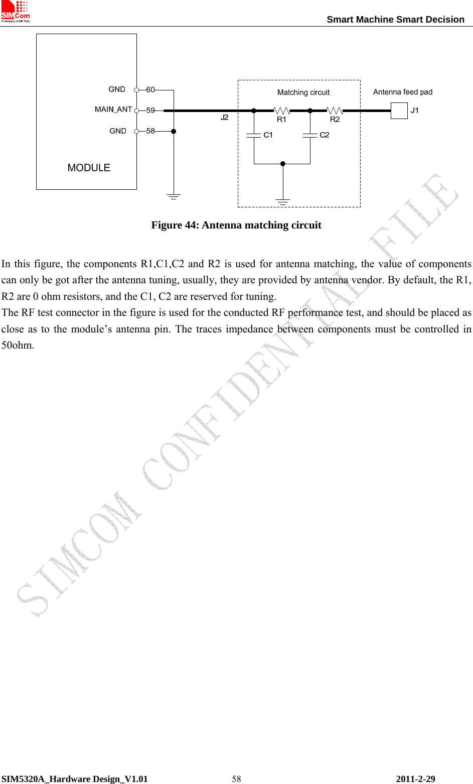
Simcom 1103022011008 GSM/GPRS/EDGE/WCDMA/HSDPA module User Manual SIM5320 HD V1 01
Shanghai Simcom Ltd. GSM/GPRS/EDGE/WCDMA/HSDPA module SIM5320 HD V1 01
UserManual.wiki
>
Simcom
>
1103022011008 User Manual
User Manual
Navigation menu
Upload a User Manual
Namespaces
Wiki Guide
HTML
PDF
Info
Views
User Manual
Discussion / Help
Navigation
![Smart Machine Smart Decision Document Title SIM5320A Hardware Design Version 1.01 Date 2011-2-29 Status Release Document Control ID SIM5320A_Hardware Design_V1.01 General Notes SIMCom offers this information as a service to its customers, to support application and engineering efforts that use the products designed by SIMCom. The information provided is based upon requirements specifically provided to SIMCom by the customers. SIMCom has not undertaken any independent search for additional relevant information, including any information that may be in the customer’s possession. Furthermore, system validation of this product designed by SIMCom within a larger electronic system remains the responsibility of the customer or the customer’s system integrator. All specifications supplied herein are subject to change. NOTICE: This device complies with Part 15 of the FCC Rules [and with RSS-210 of Industry Canada]. Operation is subject to the following two conditions: (1) this device may not cause harmful interference, and (2) this device must accept any interference received, including interference that may cause undesired operation. Changes or modifications made to this equipment not expressly approved by SIMCOM may void the FCC authorization to operate this equipment. This equipment has been tested and found to comply with the limits for a Class B digital device, pursuant to Part 15 of the FCC Rules. These limits are designed to provide reasonable protection against harmful interference in a residential installation. This equipment generates, uses and can radiate radio frequency energy and, if not installed and used in accordance with the instructions, may cause harmful interference to radio communications. However, there is no guarantee that interference will not occur in a particular installation. If this equipment does cause harmful interference to radio or television reception, which can be determined by turning the equipment off and on, the user is encouraged to try to correct the interference by one or more of the following measures: • Reorient or relocate the receiving antenna. • Increase the separation between the equipment and receiver. • Connect the equipment into an outlet on a circuit different from that to which the receiver is connected. • Consult the dealer or an experienced radio/TV technician for help. This Class [B] digital apparatus complies with Canadian ICES-003. Cet appareil numérique de la classe [B] est conforme à la norme NMB-003 du Canada.](https://usermanual.wiki/Simcom/1103022011008/User-Guide-1484828-Page-2.png)
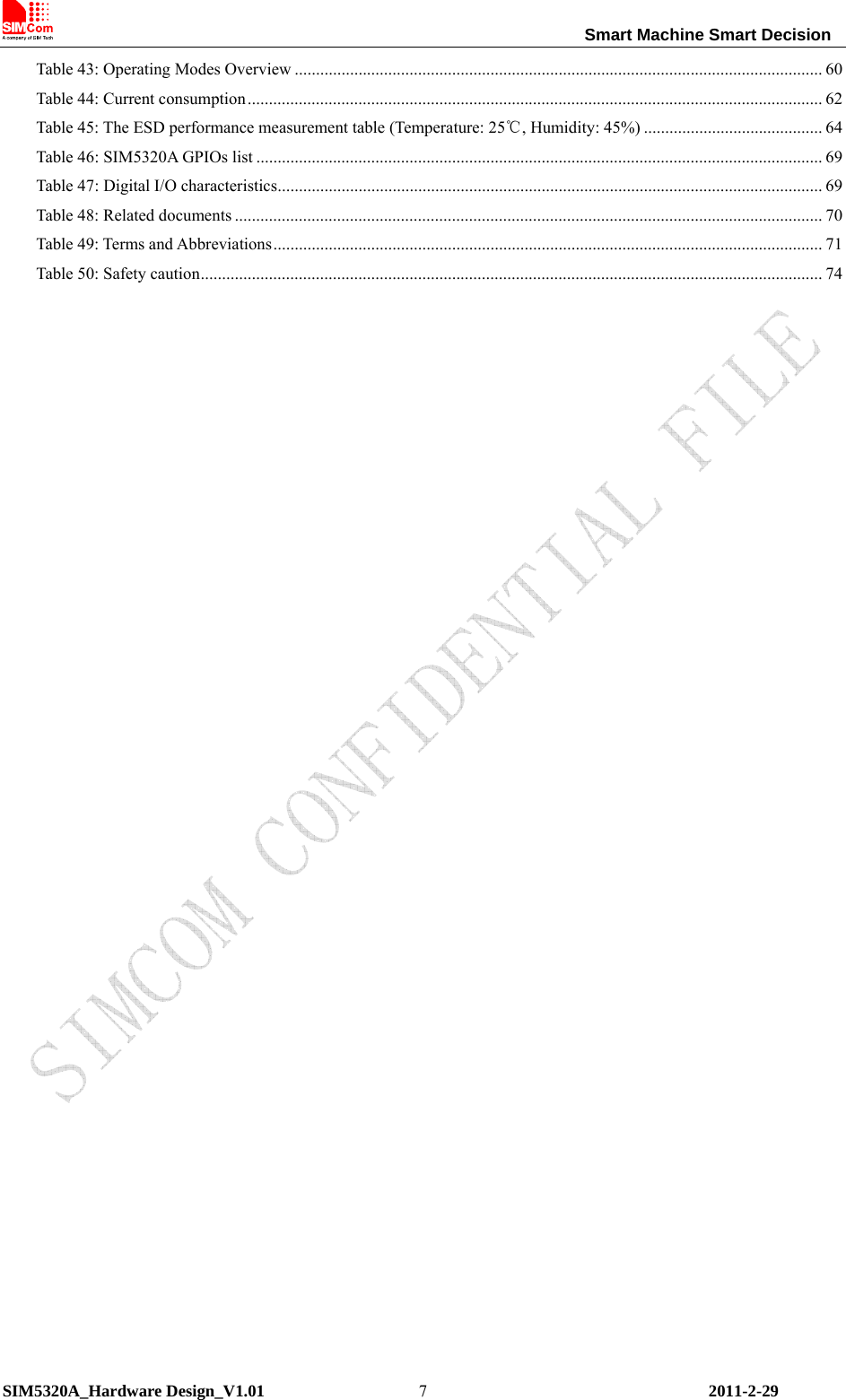
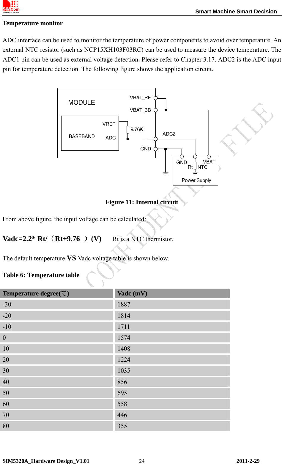
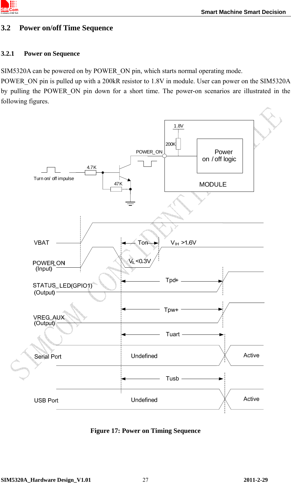
![Smart Machine Smart Decision SIM5320A_Hardware Design_V1.01 2011-2-29 23Vin VoutON/OFFGNDFB3+PWR_CTRLR102R101FB101 VBAT100K43K270 OHM+C103330uFC104100nFU101 MIC293025412C101 C102100uF 1uFDC INPUT Figure 9: Reference circuit of the LDO power supply If there is a big difference between the input voltage and the desired output (VBAT), a switching converter power will be preferable because of its better efficiency, especially at the high current situation. The following figure is the reference circuit. Note that DCDC may deprave RF performance because of ripple current intrinsically. Figure 10: Reference circuit of the DCDC power supply Voltage monitor To monitor the power supply voltage, user can use the AT command “AT+CBC”, this command has two parameters: the battery status and the voltage value (mV). It will return the capacity percentage and actual value of battery (at the VBAT_BB pin). The voltage is continuously measured at intervals, whenever the measured battery voltage is lower than a specific value set by the AT command “AT+CVALARM”. For example, if the voltage value is set to be 3.4V, the following URC will be presented: “warning! voltage is low: 3.3v”. If the voltage is lower than a specific value which is set by the AT command “AT+CPMVT”, the module will be powered off automatically and AT commands cannot be executed any more. Note: Under-voltage warning function is disabled by default, user can enable it by the AT command “AT+CVALARM”. Auto power off feature is disabled by default, user should set it by the AT command “AT+CPMVT” to an appropriate value. Please refer to Document [1].](https://usermanual.wiki/Simcom/1103022011008/User-Guide-1484828-Page-23.png)
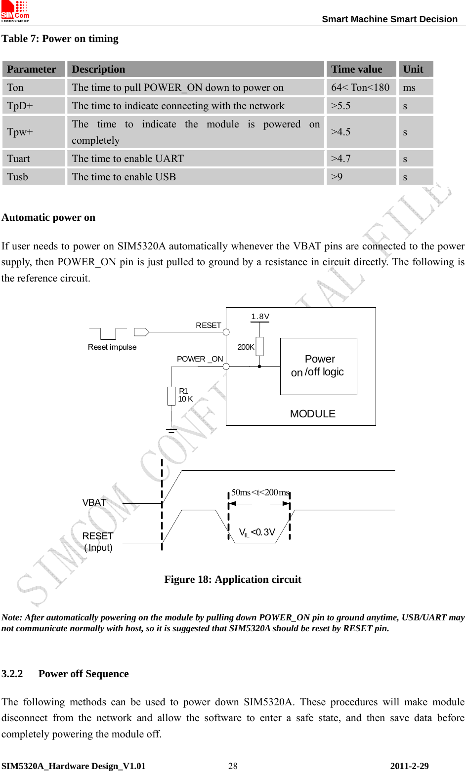
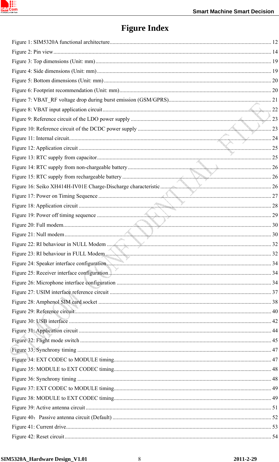
![Smart Machine Smart Decision SIM5320A_Hardware Design_V1.01 2011-2-29 29 ● Method 1: Power off SIM5320A by pulling the POWER_ON pin down ● Method 2: Power off SIM5320A by AT command User can power off the SIM5320A by pulling POWER_ON down for a specific time. The power off scenario is illustrated in the following figure. Figure 19: Power off timing sequence Table 8: Power off timing Parameter Description Time value Unit Toff The time pulling POWER_ON down to power off 0.5< Toff<5 s TpD- The time to indicate disconnecting from the network >7 s Tpw- The time to indicate the module power off completely >7.5 s Tuart_off The time to disable UART >6 s Tusb_off The time to disable USB >7.5 s User can also use the AT command “AT+ C POF ” to power down the module. After that, the AT commands cannot be executed any longer. The module enters the POWER DOWN mode, only the RTC is still active. For details, refer to Document [1].](https://usermanual.wiki/Simcom/1103022011008/User-Guide-1484828-Page-29.png)
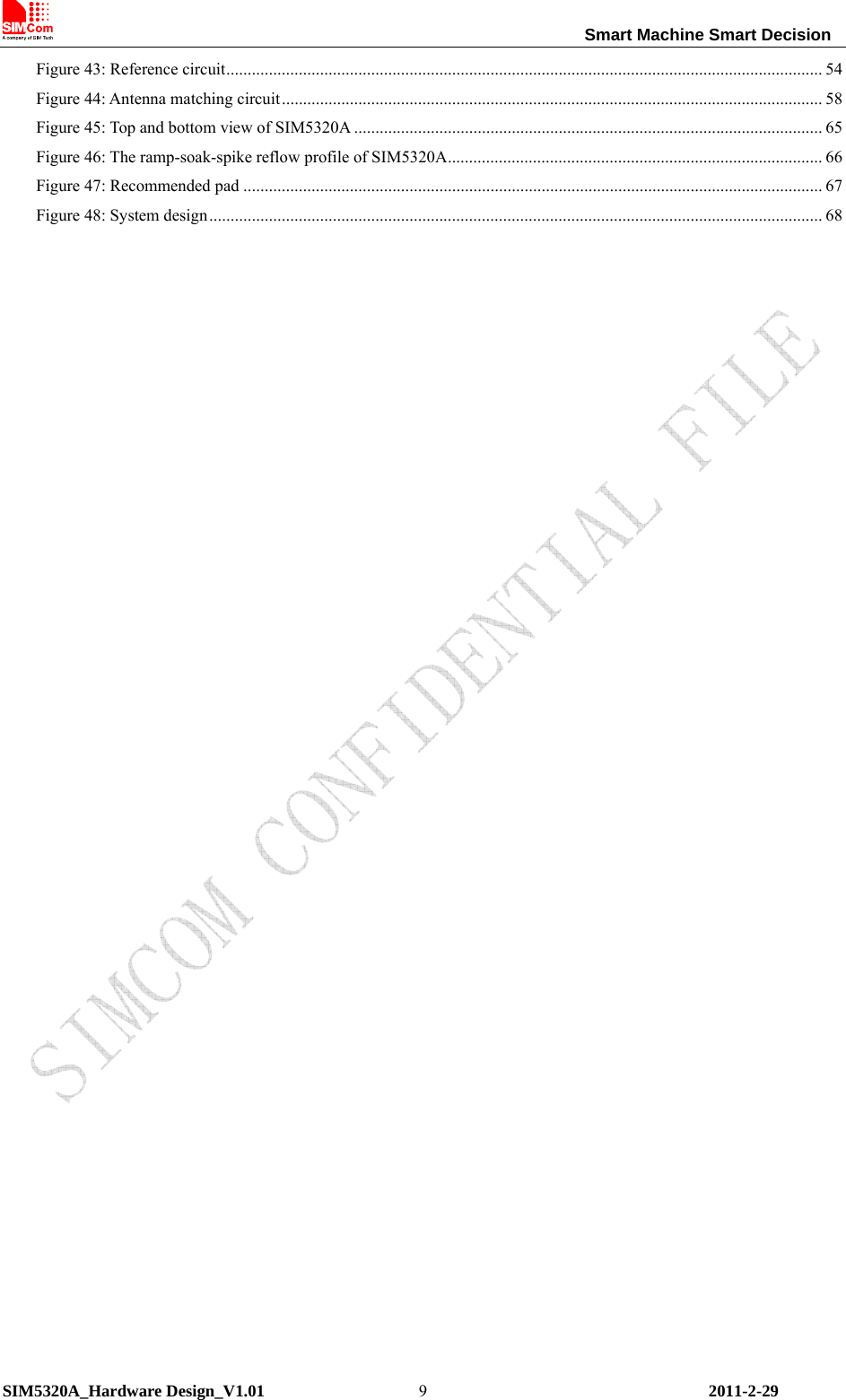
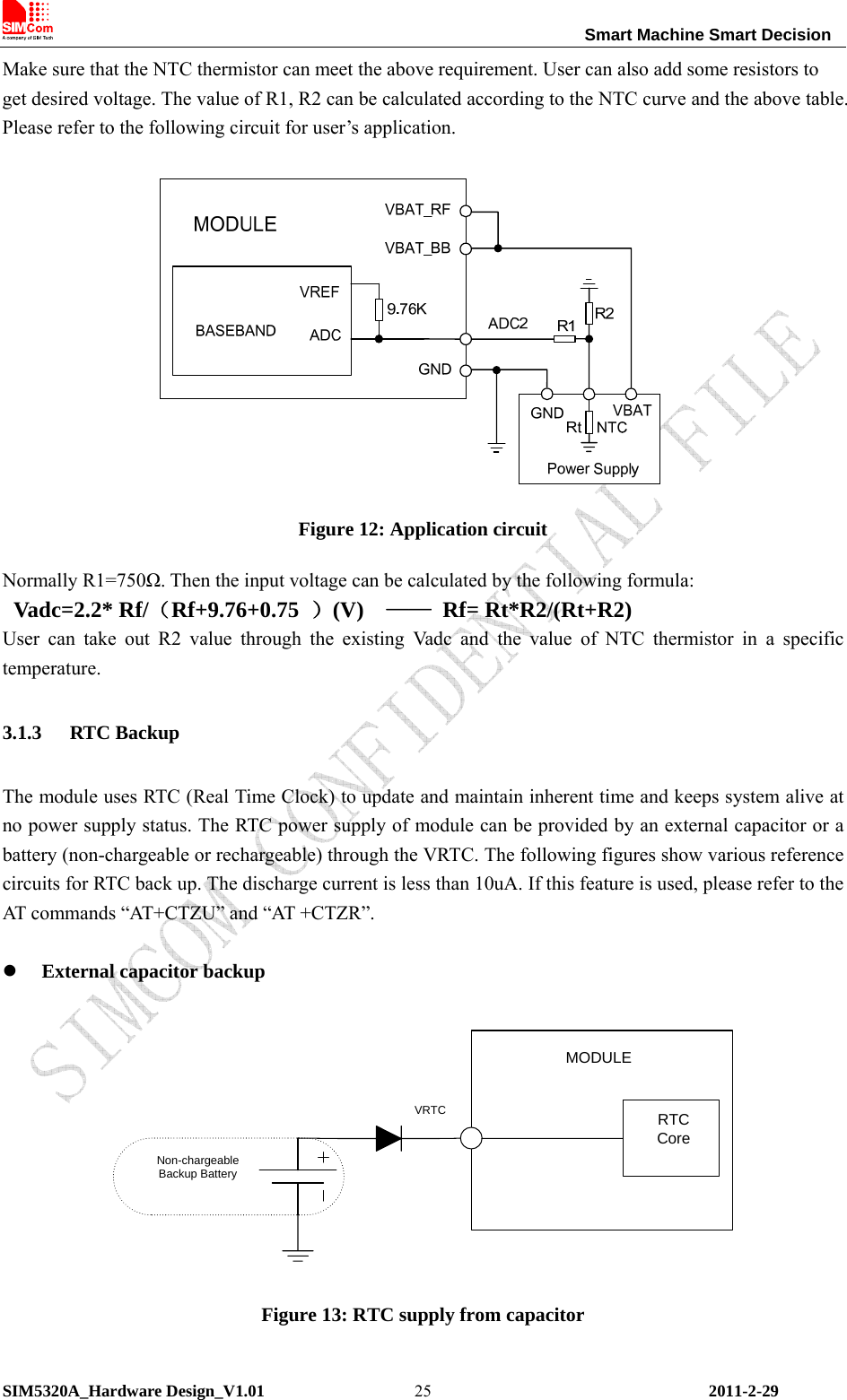
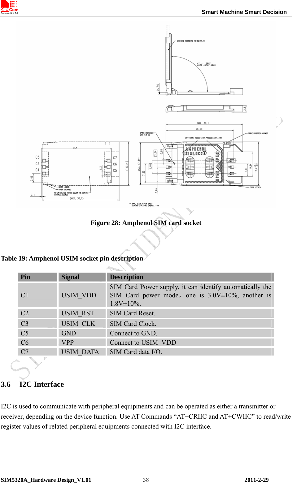
![Smart Machine Smart Decision SIM5320A_Hardware Design_V1.01 2011-2-29 37 Figure 27: USIM interface reference circuit Note: USIM_DATA has been pulled up with a 22kR resistor to V_USIM in module. A 220nF shut capacitor on V_USIM is used to reduce interference. Use AT Commands to get information in USIM card. For more detail, please refer to document [1]. 3.5.3 Recommend Components For 6 pins USIM socket, SIMCom recommend to use Amphenol C707 10M006 512 2. User can visit http://www.amphenol.com for more information about the holder.](https://usermanual.wiki/Simcom/1103022011008/User-Guide-1484828-Page-37.png)
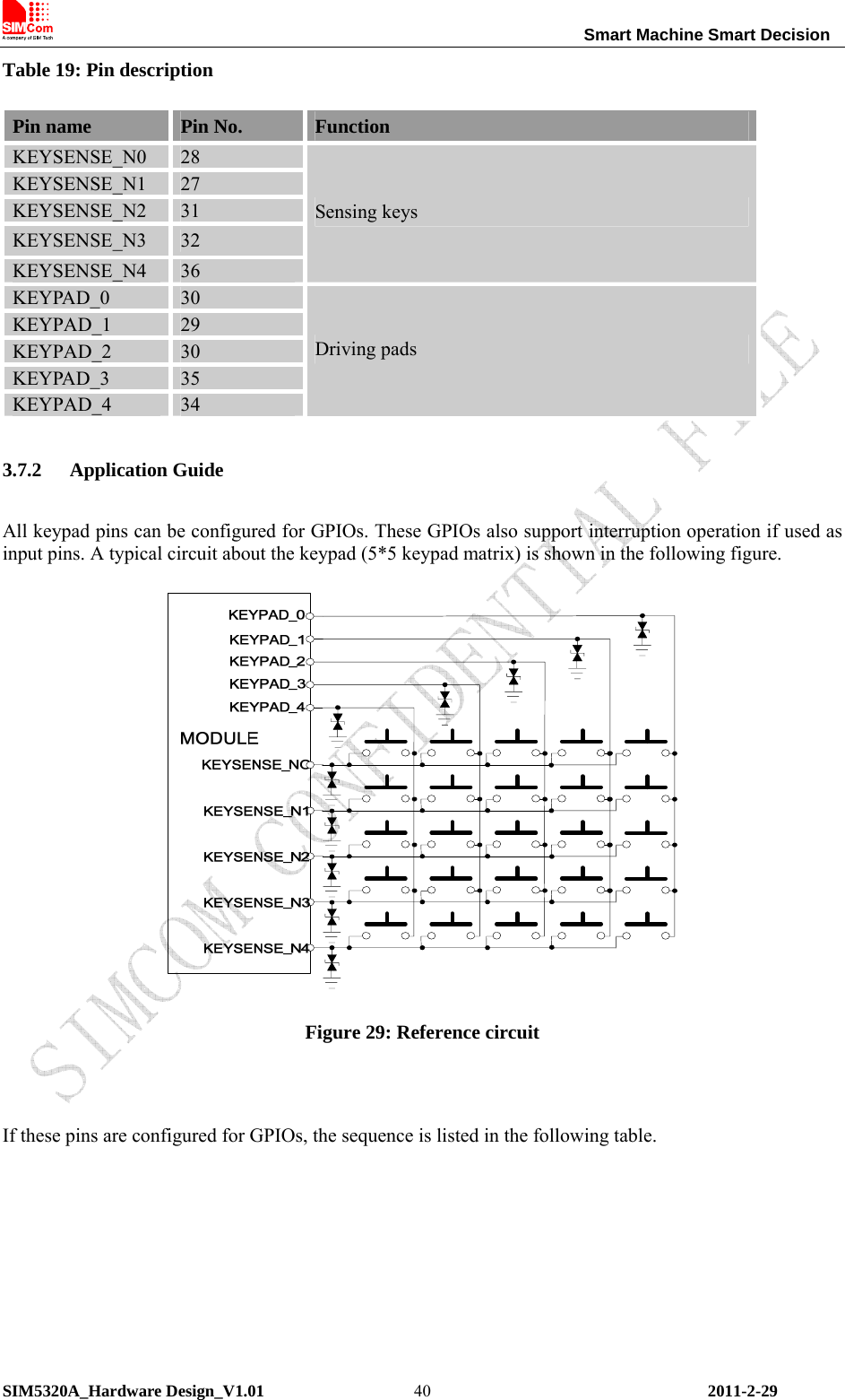
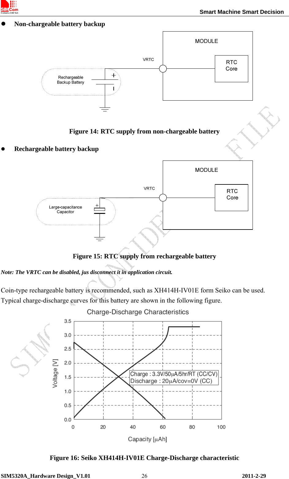
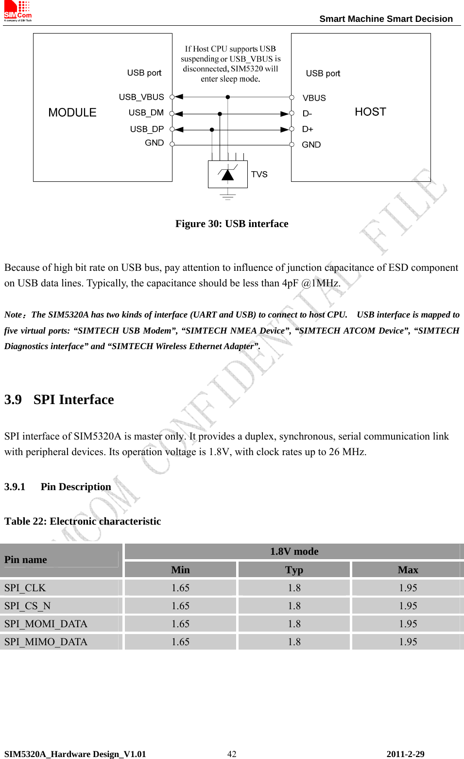
![Smart Machine Smart Decision SIM5320A_Hardware Design_V1.01 2011-2-29 41Table 20: GPIO configuration Keypad interface GPIO No. KEYPAD_4 GPIO6 KEYPAD_3 GPIO7 KEYPAD_2 GPIO8 KEYPAD_1 GPIO9 KEYPAD_0 GPIO10 KEYSENSE_N4 GPIO11 KEYSENSE_N 3 GPIO12 KEYSENSE_N 2 GPIO13 KEYSENSE_N 1 GPIO14 KEYSENSE_N 0 GPIO15 Note: Refer to document [23] for detailed information of Keypad Application Note. 3.8 USB Interface SIM5320A module contains a USB interface. This interface is compliant with the USB2.0 specification. The USB2.0 specification requires hosts such as the computer to support all three USB speeds, namely low-speed (1.5Mbps), full-speed (12Mbps) and high-speed (480Mbps). USB charging and USB-OTG is not supported. Table 21: Electronic characteristic Input voltage scope( V ) Pin name Pin No. Min Typ Max USB_VBUS 11 4.4 5.0 5.25 USB_DP 13 USB_DM 12 They are compliant with the USB 2.0 specification. 3.8.1 Application Guide Currently SIM5320A supports the USB suspend and resume mechanism which can help to save power. If no transaction is on USB bus, SIM5320A will enter suspend mode. When some events such as voice call or receiving SMS happen, SIM5320A will resume normal mode automatically.](https://usermanual.wiki/Simcom/1103022011008/User-Guide-1484828-Page-41.png)
![Smart Machine Smart Decision SIM5320A_Hardware Design_V1.01 2011-2-29 45Table 26: LED status LED Status Module Status Always On Searching Network/Call Connect 200ms ON, 200ms OFF Data Transmit 800ms ON, 800ms OFF Registered network Off Power off / Sleep Flight mode control GPIO4 controls SIM5320A module to enter or exit the Flight mode. In Flight mode, SIM5320A closes RF function to prevent interference with other equipments or minimize current consumption. Bidirectional ESD protection component is suggested to add on GPIO4. Figure 32: Flight mode switch Table 27: Control status GPIO4 Status Module operation Low Level Flight Mode: RF is closed. High Level Normal Mode: RF is working. Note:1. For SIM5320A, GPIO0, GPIO2, GPIO3 and GPIO5 have multiplex function, user can use them as PCM interface to connect extend codec. Refer to section 3.10 and document [1] for details. 2. When the module is powered off, make sure all digital interfaces (PCM UART, etc) connected with peripheral devices have no voltage higher than 0.3V. If users’ design cannot meet above conditions, high level voltages maybe occur in GPIO pins because current leakage from above digital interfaces may occur.](https://usermanual.wiki/Simcom/1103022011008/User-Guide-1484828-Page-45.png)
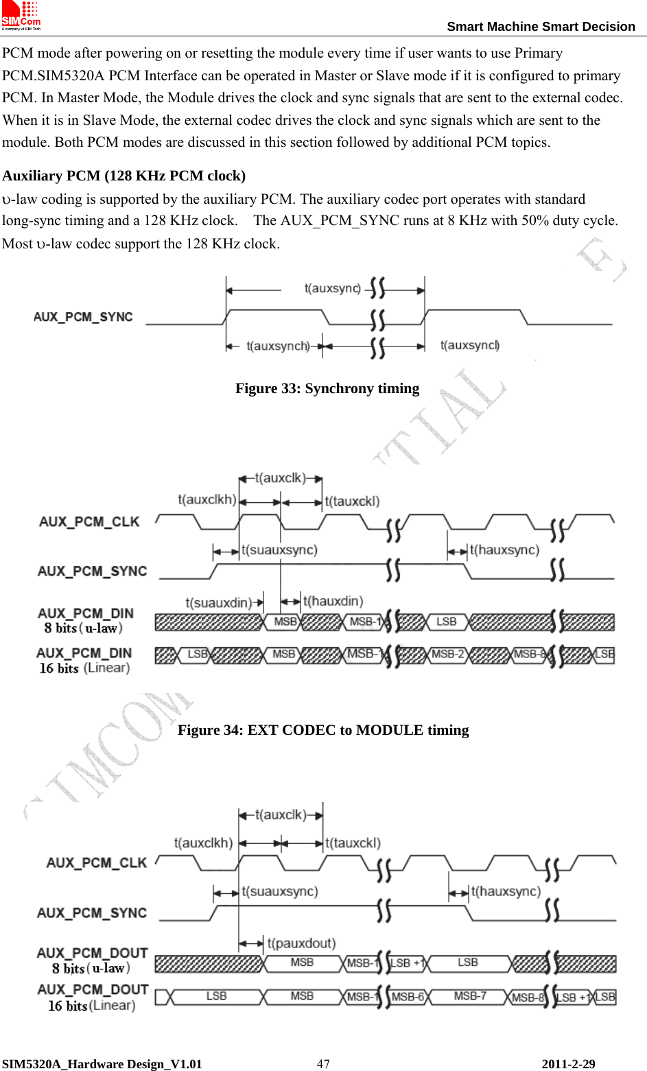
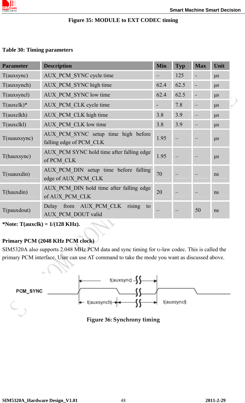
![Smart Machine Smart Decision SIM5320A_Hardware Design_V1.01 2011-2-29 463.11 PCM Interface SIM5320A provides hardware PCM interface for external codec. The PCM interface enables communication with an external codec to support hands-free applications. SIM5320A PCM interface can be used in two modes: the default mode is auxiliary PCM (8 KHz long sync mode at 128 KHz PCM CLK); the other mode is primary PCM (8 KHz short sync mode at 2048 KHz PCM CLK). In short-sync (primary PCM) mode, SIM5320A can be a master or a slave. In long-sync (auxiliary PCM) mode, SIM5320A is always a master. SIM5320A also supports 3 kinds of coding formats: 8 bits (υ-law or A-law) and 16 bits (linear). Note: PCM interface is multiplexed from GPIO (default setting). The AT command “AT+CPCM” is used to switch between PCM and GPIO functions. Please refer to document [22] and document [1] for details. 3.11.1 Pin Description Table 28: Electronic characteristic 2.6V mode Pin name Min Typ Max PCM_CLK 2.5 2.6 2.7 PCM_SYNC 2.5 2.6 2.7 PCM_DOUT 2.5 2.6 2.7 PCM_DIN 2.5 2.6 2.7 Table 29: Pin description Pins Pin No. AUX_PCM functionality Primary PCM functionality Description PCM_DIN/GPIO0 74 AUX_PCM_DIN PCM_DIN PCM data input PCM_SYNC/GPIO2 75 AUX_PCM_SYNC PCM_SYNC PCM data synchronyPCM_DOUT/GPIO5 73 AUX_PCM_DOUT PCM_DOUT PCM data output PCM_CLK/GPIO3 76 AUX_PCM_CLK PCM_CLK PCM data clock 3.11.2 Signal Description The default PCM interface in SIM5320A is the auxiliary PCM interface. The data changes on the high level of PCM_CLK and is sampled at the falling edge of PCM_CLK in one period. Primary PCM is disabled after every power-on or every reset event. So user must use AT command to enable the primary](https://usermanual.wiki/Simcom/1103022011008/User-Guide-1484828-Page-46.png)
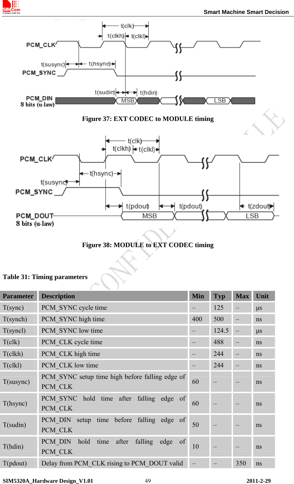
![Smart Machine Smart Decision SIM5320A_Hardware Design_V1.01 2011-2-29 50T(zdout) Delay from PCM_CLK falling to PCM_DOUT HIGH-Z – 160 – ns Note: SIM5320A can transmit PCM data by USB except for PCM interface. Please refer to document [22] for more information of PCM Application Note. 3.12 Global Positioning System SIM5320A merges GPS satellite and network information to provide a high-availability solution that offers industry-leading accuracy and performance. This solution performs well, even in very challenging environmental conditions where conventional GPS receivers fail, and provides a platform to enable wireless operators to address both location-based services and emergency mandates. 3.12.1 Technical specification Tracking sensitivity -157 dBm Cold-start sensitivity -144 dBm Accuracy (Open Sky) <2m (CEP50) TTFF (Open Sky) Hot start <1s Cold start 35s(good signal)/ 100s(weak signal) Receiver Type 12-channel, GPS L1 Frequency (1575.42MHz), C/A Code Update rate Default 1 Hz GPS data format NMEA-0183 GPS Current consumption (WCDMA/GSM Sleep mode) 100mA (Total supply current) GPS antenna Passive/Active antenna Note: Performance will vary depending on the environment, antenna type and signal conditions and so on. 3.12.2 Operate Mode SIM5320A supports both A-GPS and S-GPS, and then provides three operating modes: mobile-assisted mode, mobile-based mode and standalone mode. A-GPS includes mobile-assisted and mobile-based mode. In mobile-assisted mode, when a request for position location is issued, available network information is provided to the location server (e.g. Cell-ID) and assistance is requested from the location server. The location server sends the assistance information to the handset. The handset/mobile unit measures the GPS observables and provides the GPS measurements along with available network data (that is appropriate for the given air interface technology) to the location server. The location server then calculates the position location and returns results to the requesting entity. In mobile-based mode, the assistant data provided by the location server encompasses not only the information required to assist the handset in measuring the satellite signals, but also the information required to calculate the handset’s position. Therefore, rather than provide the GPS measurements and](https://usermanual.wiki/Simcom/1103022011008/User-Guide-1484828-Page-50.png)
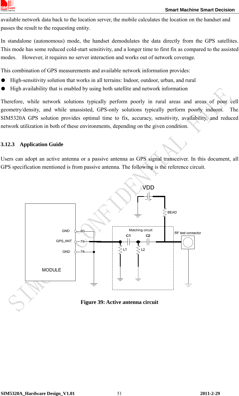
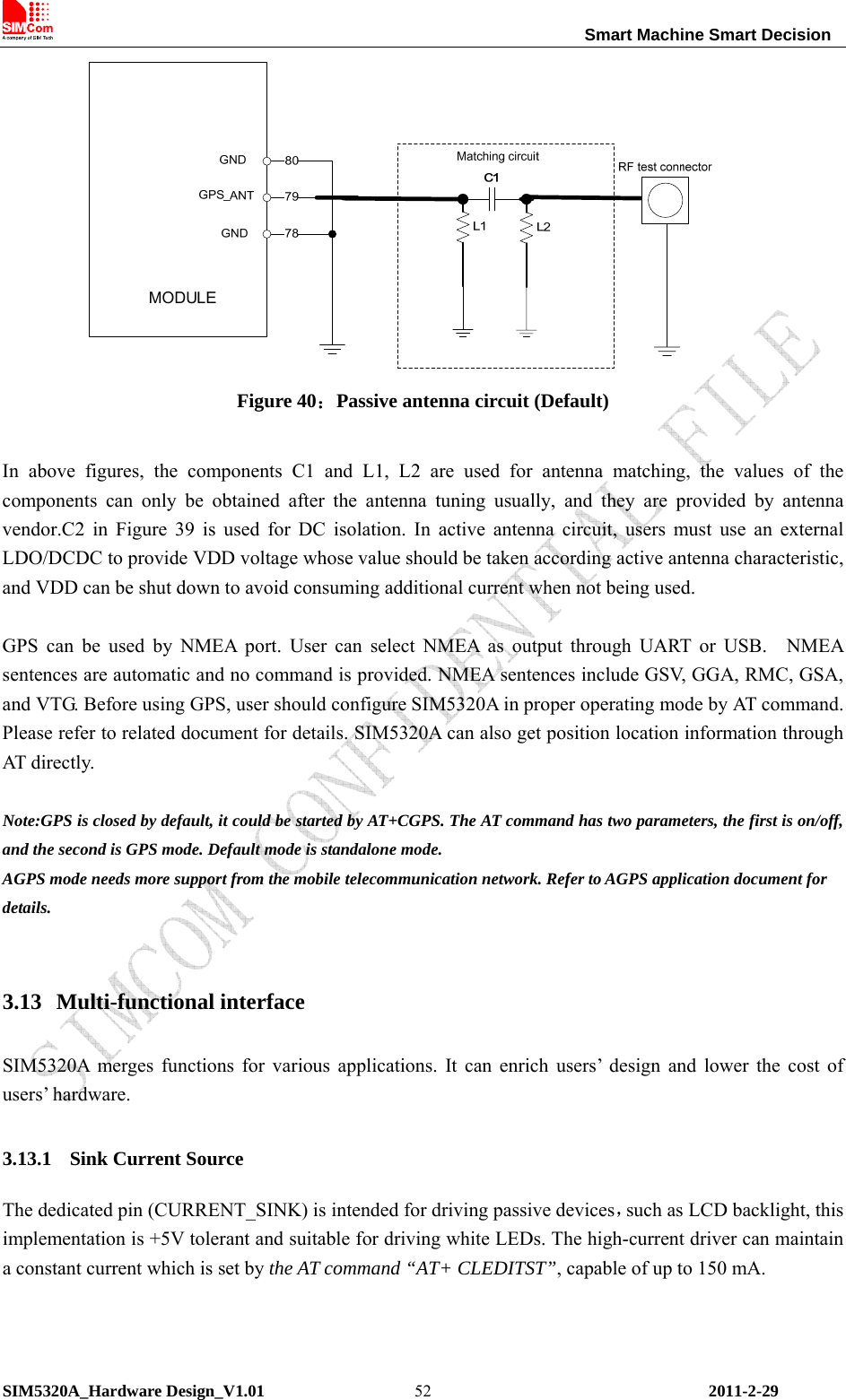
![Smart Machine Smart Decision SIM5320A_Hardware Design_V1.01 2011-2-29 54 Figure 42: Reset circuit Note:50ms<t<200ms. ESD components are suggested to be used on Reset pin. 3.13.3 ADC SIM5320A has a dedicated ADC that is available for digitizing analog signals such as battery voltage and so on; it is on PIN 47, namely ADC1. This ADC1 is 8 bit successive-approximation circuit, and electronic specification is shown in the following table. Table 33: Electronic Characteristics Specification Min Typ Max Unit Comments/Conditions Resolution 8 Bits Differential nonlinearity -4 +4 LSB Integral nonlinearity -8 +8 LSB Gain Error -2.5 +2.5 % Offset Error -4 +40 LSB Analog Vdd = ADC reference 2.4MHz sample rate Input Range GND 2.2V V Input serial resistance 2 kΩ Sample and hold switch resistance Input capacitance 53 pF Power-down to wakeup 9.6 19.2 μs User can introduce a signal in the ADC pin directly and use the AT command “AT+CADC” to get the raw data which is between 0 and 255. The data can be transformed to any type such as voltage, temperature etc. Please refer to Chapter 3.1.2 and document [1]. Figure 43: Reference circuit](https://usermanual.wiki/Simcom/1103022011008/User-Guide-1484828-Page-54.png)
![Smart Machine Smart Decision SIM5320A_Hardware Design_V1.01 2011-2-29 615.2.2 Minimize Power Consumption There are two modes that SIM5320A achieves low power consumption. Sleep mode If peripheral equipments stops working, and there is no on air or hardware interrupts (such as GPIO interrupts or data on UART), SIM5320A will enter sleep mode automatically. In this mode, SIM5320A can still receive paging,voice call or SMS from network. If USB interface of SIM5320A is connected to host CPU, but host CPU does not support USB suspending, then SIM5320A will not enter sleep mode. After USB is disconnected, SIM5320A will enter sleep mode. Note: When UART interface is connected with host CPU, SIM5320A can not enter sleep mode until RXD is pulled down by the host CPU. If the module is in the idle mode, make sure to pull the RXD to low level by host CPU. SIMCom recommends using GPIO43 or UART_DTR to wake up the module from host CPU and to use GPIO41 or UART_RI to wake up the host CPU. Before designing, pay attention to how to realize waking function and refer to Document[24] and Document[25] for more detail. Minimum functionality mode Minimum functionality mode ceases a majority function of module, thus minimizing the power consumption. This mode is set by the AT command which provides a choice of the functionality levels. ● AT+CFUN=0: Minimum functionality ● AT+CFUN=1: Full functionality (Default) ● AT+CFUN=4: Disable RF function of the module (Flight mode) If SIM5320A has been set to minimum functionality mode, the module will firstly enter sleep mode, then the RF function and SIM card function will be closed. In this case, the serial port is still accessible, but RF function or SIM card will be unavailable. When SIM5320A is in minimum functionality or flight mode, it can return to full functionality by the AT command “AT+CFUN=1”. Note: For flight mode, please refer to Chapter 2.12.2. 5.3 Current Consumption The current consumption in suspended mode and without USB connection is listed in the table below. Here, “suspended mode” means that SIM5320A is connected to USB bus, but it does not transfer data.](https://usermanual.wiki/Simcom/1103022011008/User-Guide-1484828-Page-61.png)
![Smart Machine Smart Decision SIM5320A_Hardware Design_V1.01 2011-2-29 66 Figure 46: The ramp-soak-spike reflow profile of SIM5320A For details about secondary SMT, please refer to document [26]. 6.3 Moisture Sensitivity Level (MSL) SIM5320A is qualified to Moisture Sensitivity Level (MSL) 3 in accordance with JEDEC J-STD-020. After the prescribed time limit exceeded, users should bake modules for 192 hours in drying equipment (<5% RH) at 40° C +5° C/-0° C, or 72 hours at 85° C +5° C/-5° C. Note that plastic tray is not heat-resistant, users must not use the tray to bake at 85° C or the tray may be damaged. 6.4 Stencil Foil Design Recommendation The recommended thickness of stencil foil is more than 0.18mm.](https://usermanual.wiki/Simcom/1103022011008/User-Guide-1484828-Page-66.png)
![Smart Machine Smart Decision SIM5320A_Hardware Design_V1.01 2011-2-29 69B. SIM5320A GPIOs List Table 46: SIM5320A GPIOs list Name GPIO Index Default Function Alternate Function PCM_DIN 0 GPIO Interrupt [LEVEL/LOW] PCM_DIN STATUS_LED 1 Status led GPIO PCM_SYNC 2 GPIO [IN] PCM_SYNC PCM_CLK 3 GPIO [OUT/LOW] PCM_CLK RF_SWITCH 4 RF Switch Enable/Disable RF subsystem PCM_OUT 5 GPIO [OUT/LOW] PCM_OUT KEYPAD_4 6 Keypad GPIO KEYPAD_3 7 Keypad GPIO KEYPAD_2 8 Keypad GPIO KEYPAD_1 9 Keypad GPIO KEYPAD_0 10 Keypad GPIO KEYSENSE_N4 11 Keypad GPIO KEYSENSE_N3 12 Keypad GPIO KEYSENSE_N2 13 Keypad GPIO KEYSENSE_N1 14 Keypad GPIO KEYSENSE_N0 15 Keypad GPIO UART1_CTS 33 CTS GPIO UART1_RFR 34 RTS GPIO UART1_DTR 35 DTR wake up module GPIO UART_DCD 36 DCD GPIO UART_RI 37 RI wake up host GPIO GPIO40 40 Module power up status GPIO GPIO41 41 Wake up host GPIO GPIO42 42 GPIO GPIO GPIO43 43 Wake up module GPIO GPIO44 44 GPIO GPIO C. Digital I/O Characteristics Table 47: Digital I/O characteristics 2.6V Mode 1.8V Mode Parameter Description Min Typ Max Min Typ Max Unit VREG_AUX LDO output 0 2.6 2.9 0 1.8 1.84 V VIH High-level input voltage 1.69 2.6 2.9 1.17 1.8 2.1 V VIL Low-level input voltage -0.3 0 0.91 -0.3 0 0.63 V VOH High-level 1.17 2.6 2.6 0.81 1.8 1.8 V](https://usermanual.wiki/Simcom/1103022011008/User-Guide-1484828-Page-69.png)
![Smart Machine Smart Decision SIM5320A_Hardware Design_V1.01 2011-2-29 70output voltage VOL Low-level output voltage 0 0 0.45 0 0 0.45 V IIH Input high leakage current - - 1 - - 1 uA IIL Input low leakage current -1 - - -1 - - uA CIN Input capacitance - - 7 - - 7 pF Note: These parameters are for digital interface pins, such as keypad, GPIO, I2C, UART, SPI and DEBUG. The SIM5320A includes two kinds of voltages: 1.8v and 2.6v. Digital I/O specifications under both conditions are presented in the above tables. D. Related Documents Table 48: Related documents SN Document name Remark [1] SIM5320A_ATC_V1.00 SIM5320A_ATC_V1.00 [2] ITU-T Draft new recommendationV.25ter Serial asynchronous automatic dialing and control [3] GSM 07.07 Digital cellular telecommunications (Phase 2+); AT command set for GSM Mobile Equipment (ME) [4] GSM 07.10 Support GSM 07.10 multiplexing protocol [5] GSM 07.05 Digital cellular telecommunications (Phase 2+); Use of Data Terminal Equipment – Data Circuit terminating Equipment (DTE – DCE) interface for Short Message Service (SMS) and Cell Broadcast Service (CBS) [6] GSM 11.14 Digital cellular telecommunications system (Phase 2+); Specification of the SIM Application Toolkit for the Subscriber Identity Module – Mobile Equipment (SIM – ME) interface [7] GSM 11.11 Digital cellular telecommunications system (Phase 2+); Specification of the Subscriber Identity Module – Mobile Equipment (SIM – ME) interface [8] GSM 03.38 Digital cellular telecommunications system (Phase 2+); Alphabets and language-specific information [9] GSM 11.10 Digital cellular telecommunications system (Phase 2); Mobile Station (MS) conformance specification; Part 1: Conformance specification [10] 3GPP TS 51.010-1 Digital cellular telecommunications system (Release 5); Mobile Station (MS) conformance specification [11] 3GPP TS 34.124 Electromagnetic Compatibility (EMC) for mobile terminals and](https://usermanual.wiki/Simcom/1103022011008/User-Guide-1484828-Page-70.png)
![Smart Machine Smart Decision SIM5320A_Hardware Design_V1.01 2011-2-29 71ancillary equipment. [12] 3GPP TS 34.121 Electromagnetic Compatibility (EMC) for mobile terminals and ancillary equipment. [13] 3GPP TS 34.123-1 Technical Specification Group Radio Access Network; Terminal conformance specification; Radio transmission and reception (FDD) [14] 3GPP TS 34.123-3 User Equipment (UE) conformance specification; Part 3: Abstract Test Suites. [15] EN 301 908-02 V2.2.1 Electromagnetic compatibility and Radio spectrum Matters (ERM); Base Stations (BS) and User Equipment (UE) for IMT-2000. Third Generation cellular networks; Part 2: Harmonized EN for IMT-2000, CDMA Direct Spread (UTRA FDD) (UE) covering essential requirements of article 3.2 of the R&TTE Directive [16] EN 301 489-24 V1.2.1 Electromagnetic compatibility and Radio Spectrum Matters (ERM); Electromagnetic Compatibility (EMC) standard for radio equipment and services; Part 24: Specific conditions for IMT-2000 CDMA Direct Spread (UTRA) for Mobile and portable (UE) radio and ancillary equipment [17] IEC/EN60950-1(2001) Safety of information technology equipment (2000) [18] 3GPP TS 51.010-1 Digital cellular telecommunications system (Release 5); Mobile Station (MS) conformance specification [19] GCF-CC V3.23.1 Global Certification Forum - Certification Criteria [20] 2002/95/EC Directive of the European Parliament and of the Council of 27 January 2003 on the restriction of the use of certain hazardous substances in electrical and electronic equipment (RoHS) [21] Audio Application Note V1.01 Audio Application Note V1.01 [22] PCM Application Note V1.02 PCM Application Note V1.02 [23] Keypad Application Note V1.01 Keypad Application Note V1.01 [24] Sleep_Application_Note Sleep_Application_Note [25] Waking_up_Application_Note Waking_up_Application_Note [26] Module secondary-SMT-UGD SMT Note E. Terms and Abbreviations Table 49: Terms and Abbreviations Abbreviation Description ADC Analog-to-Digital Converter ARP Antenna Reference Point BER Bit Error Rate BTS Base Transceiver Station CS Coding Scheme](https://usermanual.wiki/Simcom/1103022011008/User-Guide-1484828-Page-71.png)