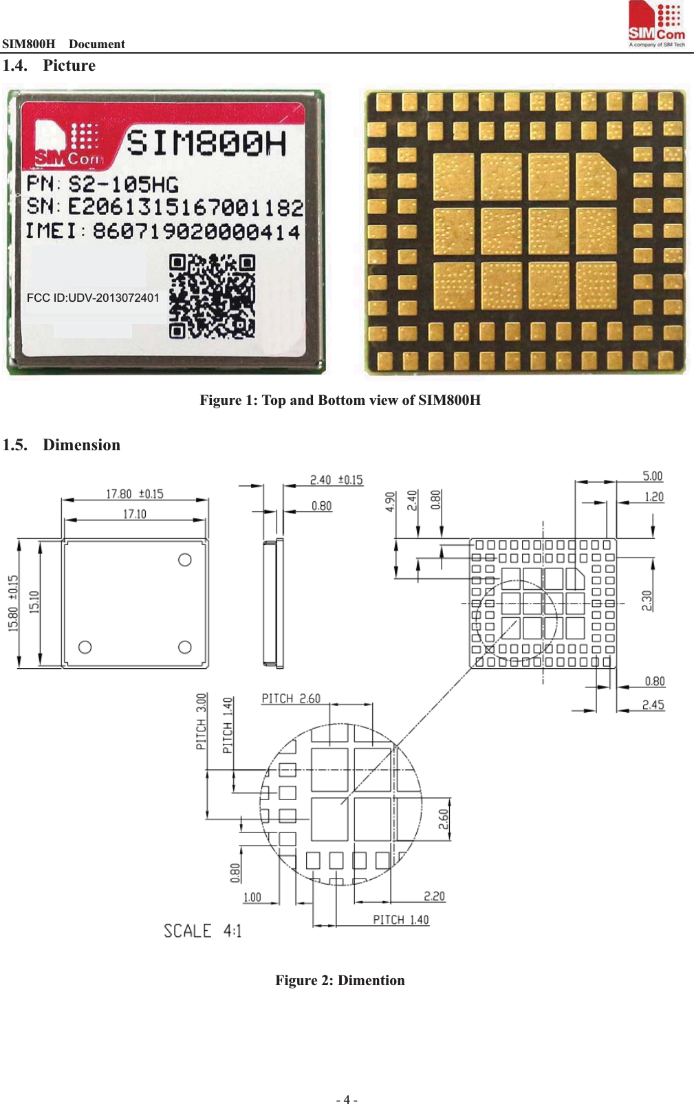
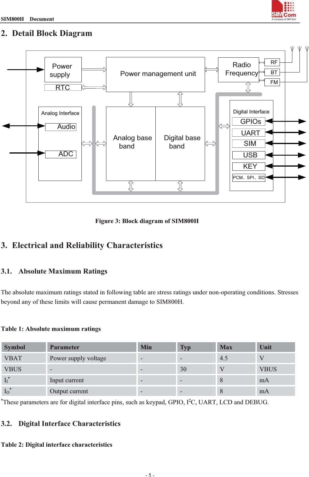
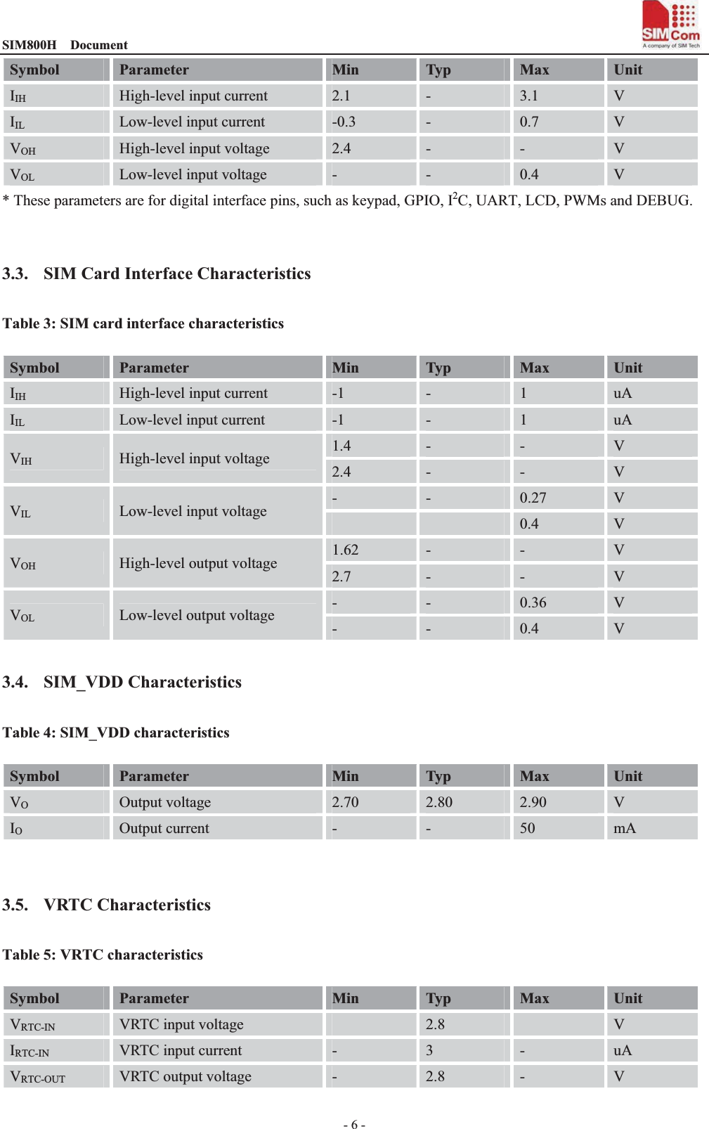
Simcom 2013072401 GSM/GPRS/BT Wireless Data Module User Manual
Shanghai Simcom Ltd. GSM/GPRS/BT Wireless Data Module
UserManual.wiki
>
Simcom
>
2013072401 User Manual
User Manual
Navigation menu
Upload a User Manual
Namespaces
Wiki Guide
HTML
PDF
Info
Views
User Manual
Discussion / Help
Navigation
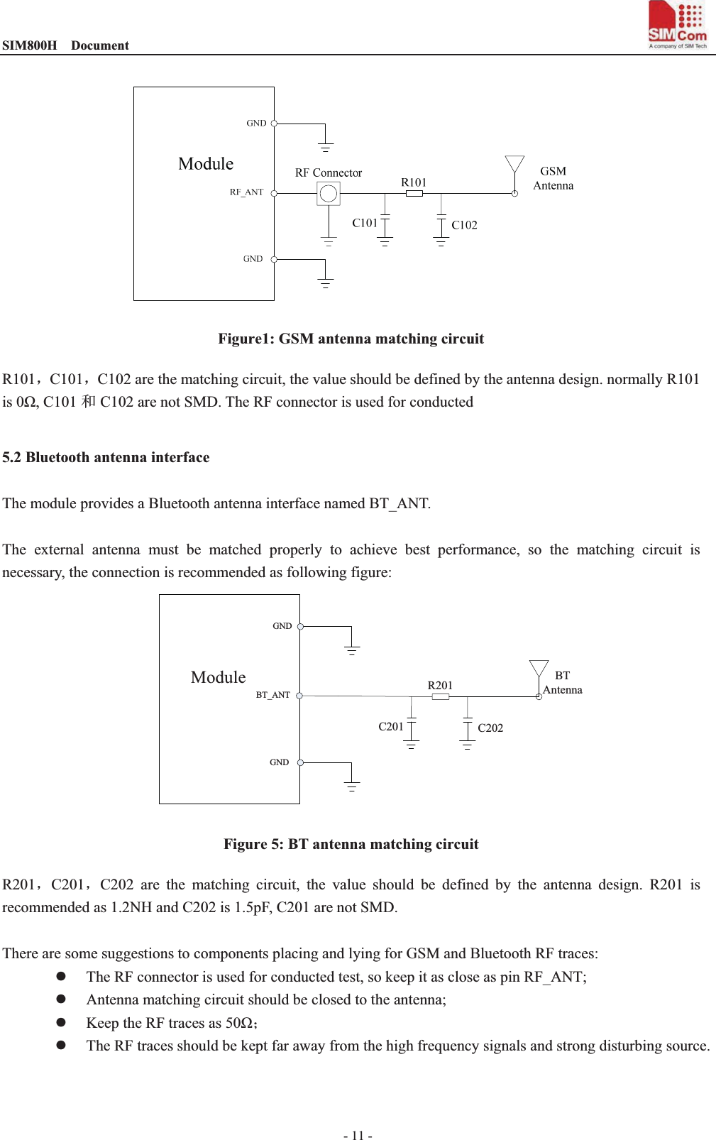
![SIM800H Document - 10 - 4.2. Module RF Receive Sensitivity The following table shows the module’s conducted receive sensitivity, it is tested under static condition. Table 10: SIM800H conducted RF receive sensitivity Frequency Receive sensitivity˄Typical˅Receive sensitivity(Max) GSM850 -108dBm -106dBm EGSM900 -108dBm -106dBm DCS1800 -108dBm -106dBm PCS1900 -108dBm -106dBm 4.3. Module Operating Frequencies The following table shows the module’s operating frequency range; it is followed by the 3GPP TS 05.05 technical specification requirement. Table 11: SIM800H operating frequencies Frequency Receive Transmit GSM850 869 ~ 894MHz 824 ~ 849 MHz EGSM900 925 ~ 960MHz 880 ~ 915MHz DCS1800 1805 ~ 1880MHz 1710 ~ 1785MHz PCS1900 1930 ~ 1990MHz 1850 ~ 1910MHz 5. Antenna interface There are three antenna ports for SIM800H, GSM antenna port named RF_ANT, Bluetooth antenna port named BT_ANT and FM antenna port named FM_ANT_P, The RF interface of the three antenna ports has an impedance of 50.The maximum gain of the GSM antenna gain should not exceed 3dBi considering the SAR radio. And the maximum gain of the Bluetooth antenna gain shout not exceed 2dBi.1RDQWHQQDJDLQPD\EHXVHGWKDWZRXOGH[FHHGWKH:(,53SRZHUOLPLWLQ0+]EDQG zThe input impendence of the antenna should be 50, and the VSWR should be less than 2. zIt is recommended that the GSM antenna and the BT antenna be placed as far as better. zThe isolations of the three antenna should be bigger than 30d% 5.1 GSM Antenna Interface There is a GSM antenna pad named RF_ANT for SIM800H the connection of the antenna must be decoupled from DC voltage. This is necessary because the antenna connector is DC coupled to ground via an inductor for ESD protection. The external antenna must be matched properly to achieve best performance, so the matching circuit is necessary, the connection is recommended as following:](https://usermanual.wiki/Simcom/2013072401/User-Guide-2039740-Page-10.png)