Simcom 2013072401 GSM/GPRS/BT Wireless Data Module User Manual
Shanghai Simcom Ltd. GSM/GPRS/BT Wireless Data Module
Simcom >
User Manual

SIM800H Document
- 1 -
SIM800H User Manual
Compliance Information
FCC Compliance Statement: This device complies with Part 15 of the FCC Rules . Operation is subject to the
following two conditions: 1. This device may not cause harmful interference, and 2. This device must accept
any interference received, including interference that may cause undesired operation. This device must accept
any interference received, including interference that may cause undesired operation. Product that is a radio
transmitter is labeled with FCC ID.
FCC Caution:
(1)Exposure to Radio Frequency Radiation. This equipment must be installed and operated in accordance with
provided instructions and the antenna(s) used for this transmitter must be installed to provide a separation
distance of at least 20 cm from all persons and must not be collocated or operating in conjunction with any other
antenna or transmitter. End-users and installers must be provided with antenna installation instructions and
transmitter operating conditions for satisfying RF exposure compliance.
(2) Any changes or modifications not expressly approved by the grantee of this device could void the user's
authority to operate the equipment.
(3) This Transmitter must not be co-located or operating in conjunction with any other antenna or transmitter.
(4) Changes or modifications to this unit not expressly approved by the party responsible for compliance could
void the user authority to operate the equipment.
(5) the modules FCC ID is not visible when installed in the host, or
(6) if the host is marketed so that end users do not have straight forward commonly used methods for access to
remove the module so that the FCC ID of the module is visible; then an additional permanent label referring to
the enclosed module: Contains Transmitter Module FCC ID: UDV-2013072401 or Contains FCC ID:
UDV-2013072401 must be used.
1. SIM800H Description
1.1. Summarize
SIM800H designed by SIMCom is a quad band module which supports GSM/GPRS. The baseband circuit is
based on MTK and RF circuit is based on RFMD. It works at quad bands------GSM850, EGSM900, DCS1800,
and PCS1900. CPU clock is based on 26MHz crystal. The main IC includes MT6260D and RF7176.
1.2. Feature
ƽ Quad-Band 850/900/1800/1900MHz
ƽ GPRS multi-slot class 12/10
ƽ GPRS mobile station class B
ƽ Bluetooth output power class 1
ƽ Bluetooth v3.0 with data rates 3.0Mbps
ƽ Compliant to GSM phase 2/2+

SIM800H Document
- 2 -
–Class 4 (2 W @ 850/900 MHz)
–Class 1 (1 W @ 1800/1900MHz)
ƽ Dimensions: 15.8*17.8*2.4 mm
ƽ Weight: 1.25 g
ƽ Control via AT commands (3GPP TS 27.007, 27.005 and SIMCom enhanced AT Commands)
ƽ Supply voltage range 3.6~4.2 V
ƽ Low power consumption
ƽ Operation temperature:-30~80ć
ƽ 88 LGA pads include
–Interface to external SIM 3V/1.8V
–Analog audio interface
–RTC backup
–Serial interface
–USB interface
–Keypad interface
–LCD interface
–Antenna pad
–PCM
–GPIO
–ADC
SIM800H Document
- 3 -
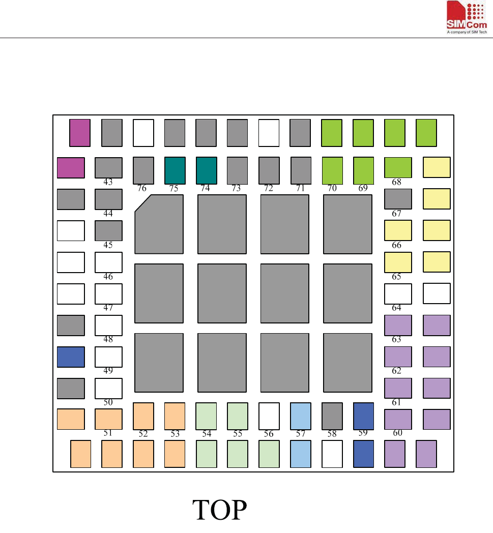
1.3. Pin
GND
VBAT
VBAT
GPIO
1
GND
GND
ISINK0
USB_DP
USB_
DP
GND
GND
STATUS ISINK1
VBUS
ADC
RESET
GND
PCMIN
PCM
CLK
GPIO
3
ROW4
ROW0
ROW1 COL2
COL0
GND
PWM
COL4
ROW3ROW2
COL3
COL1
VRTC
ANT RXD
PWR
KEY
CTS TXDRTS
SCL
SDA UART
_DTR
BPI_
BUS1
UART
_DCD
UART_
RI
PCM
OUT
PCM
SYNC
NETLI
GHT
SPK1P
MIC1P
MIC1N
MIC2P
MIC2N
GND
VSIM
SIM_
RST
SPK1NSPK2N
SPK2P
BT_
ANT
SIM_
CLK
SIM
PRE
SIM_
DATA
VDD
EXT
GND
86 85 84
GND 87 88 83
GND 80 81 82
1
2
3
4
5
6
7
8
9
10
FM_
ANT_N
FM_
ANT_P
USB_
DM
GNDGND
GND
GNDGND
GND
GND
GND
78
79
21
22
30
3142
GPIO
2
11 12 13 14 15 16 17 18 19 20
23
24
25
26
27
28
29
40 39 38 37 36 35 34 33 3241
77
SIM800H Document
- 4 -
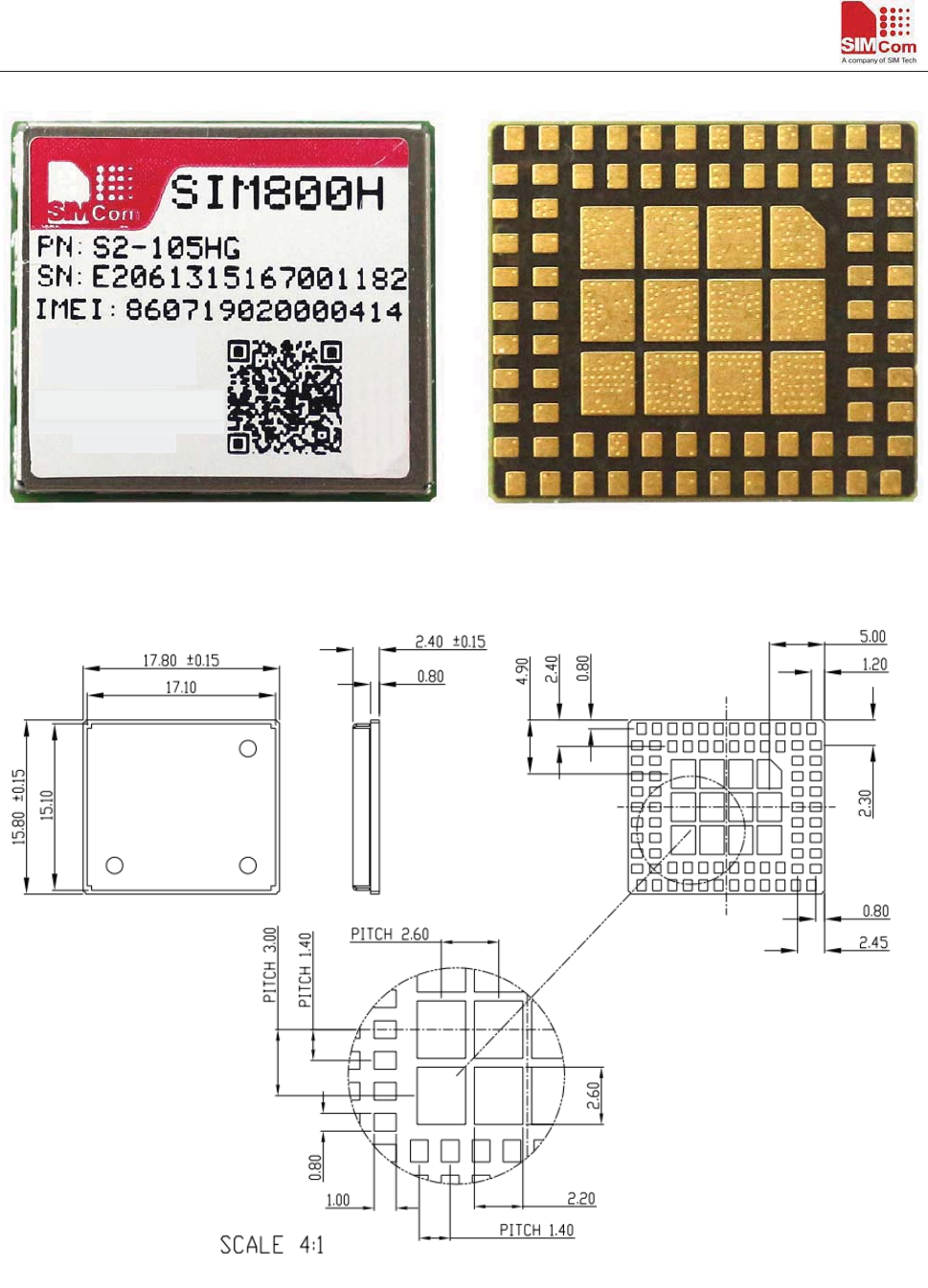
1.4. Picture
Figure 1: Top and Bottom view of SIM800H
1.5. Dimension
Figure 2: Dimention
FCC ID:2013-072401
FCC ID:UDV-2013072401
SIM800H Document
- 5 -
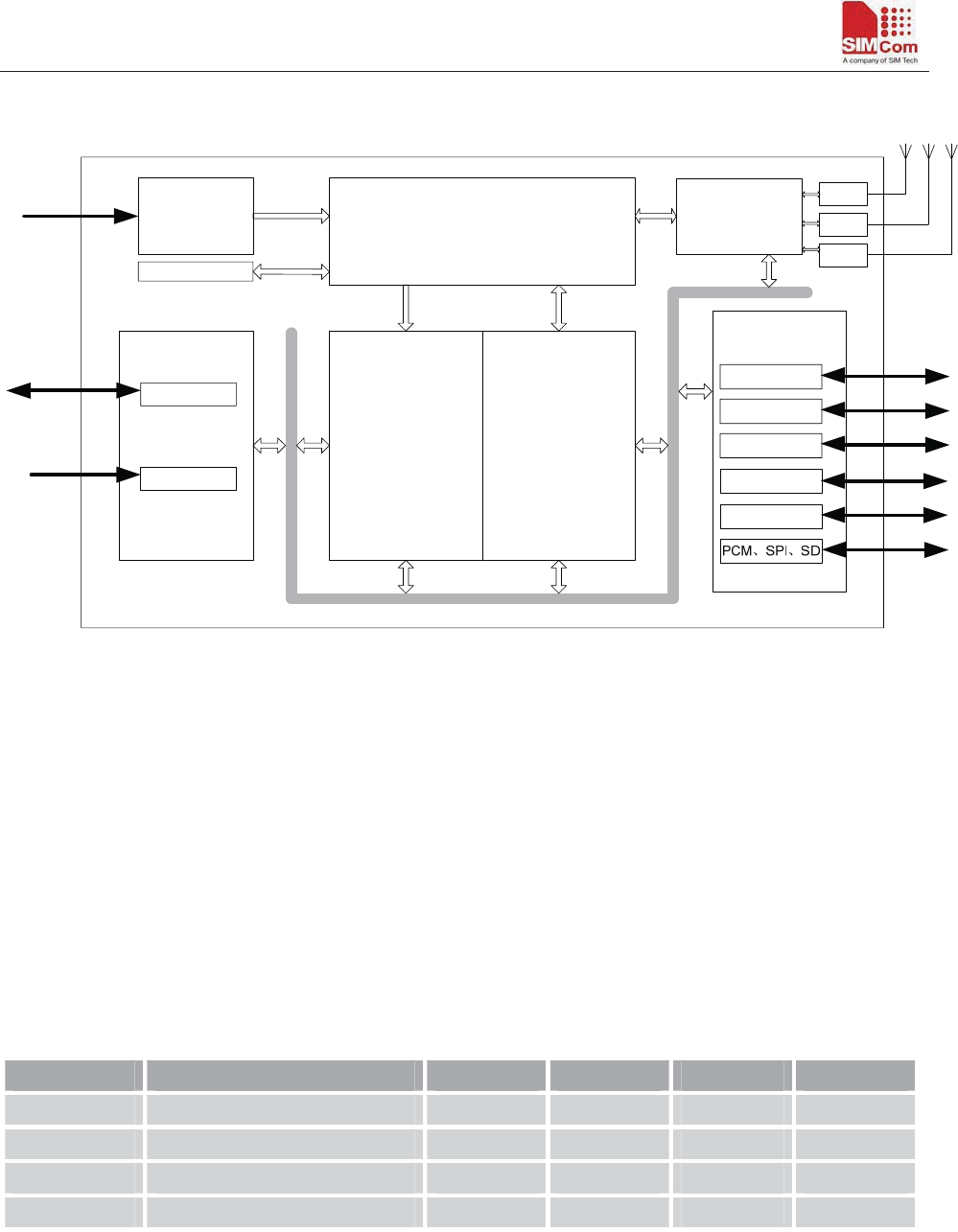
2. Detail Block Diagram
Analog base
band
Digital base
band
Power management unit
Radio
Frequency
Power
supply
Analog Interface Digital Interface
UART
SIM
GPIOs
RTC
Audio
ADC
RF
BT
FM
USB
KEY
Figure 3: Block diagram of SIM800H
3. Electrical and Reliability Characteristics
3.1. Absolute Maximum Ratings
The absolute maximum ratings stated in following table are stress ratings under non-operating conditions. Stresses
beyond any of these limits will cause permanent damage to SIM800H.
Table 1: Absolute maximum ratings
Symbol Parameter Min Typ Max Unit
VBAT Power supply voltage - - 4.5 V
VBUS - - 30 V VBUS
II* Input current - - 8 mA
IO* Output current - - 8 mA
*These parameters are for digital interface pins, such as keypad, GPIO, I2C, UART, LCD and DEBUG.
3.2. Digital Interface Characteristics
Table 2: Digital interface characteristicsȱ
SIM800H Document
- 6 -
Symbol Parameter Min Typ Max Unit
IIH High-level input current 2.1 - 3.1 V
IIL Low-level input current -0.3 - 0.7 V
VOH High-level input voltage 2.4 - - V
VOL Low-level input voltage - - 0.4 V
* These parameters are for digital interface pins, such as keypad, GPIO, I2C, UART, LCD, PWMs and DEBUG.
3.3. SIM Card Interface Characteristics
Table 3: SIM card interface characteristicsȱ
Symbol Parameter Min Typ Max Unit
IIH High-level input current -1 - 1 uA
IIL Low-level input current -1 - 1 uA
VIH High-level input voltage 1.4 - - V
2.4 - - V
VIL Low-level input voltage - - 0.27 V
0.4 V
VOH High-level output voltage 1.62 - - V
2.7 - - V
VOL Low-level output voltage - - 0.36 V
- - 0.4 V
3.4. SIM_VDD Characteristics
Table 4: SIM_VDD characteristicsȱ
Symbol Parameter Min Typ Max Unit
VO Output voltage 2.70 2.80 2.90 V
IO Output current - - 50 mA
3.5. VRTC Characteristics
Table 5: VRTC characteristicsȱ
Symbol Parameter Min Typ Max Unit
VRTC-IN VRTC input voltage 2.8 V
IRTC-IN VRTC input current - 3 - uA
VRTC-OUT VRTC output voltage - 2.8 - V
SIM800H Document
- 7 -
IRTC-OUT VRTC output current - 2 mA
3.6. Current Consumption (VBAT = 3.8V)
Table 6: Current consumptionȱ
Symbol Parameter Conditions Value Unit
IVRTC VRTC current VBAT disconnects. Backup battery is 3 V 2 uA
IVBAT VBAT current
Power down mode 50 uA
Sleep mode
BS-PA-MFRMS=9 1.0
mA BS-PA-MFRMS=5 1.2
BS-PA-MFRMS=2 1.8
Idle mode
GSM 850
19 mA
EGSM 900
DCS 1800
PCS 1900
Voice call
GSM 850
EGSM 900
PCL=5 250
mA
PCL=12 110
PCL=19 76
DCS 1800
PCS 1900
PCL=0 168
PCL=7 89
PCL=15 76
Data mode
GPRS(1Rx,1Tx)
GSM 850
EGSM 900
PCL=5 240
mA PCL=12 110
PCL=19 83
DCS 1800
PCS 1900
PCL=0 170
mA PCL=7 95
PCL=15 80
Data mode
GPRS(4Rx,1Tx)
GSM 850
EGSM 900
PCL=5 270
mA PCL=12 150
PCL=19 120
DCS 1800
PCS 1900
PCL=0 205
mA PCL=7 130
PCL=15 115
Data mode
GPRS(3Rx,2Tx)
GSM 850
EGSM 900
PCL=5 440
mA PCL=12 185
PCL=19 130
DCS 1800
PCS 1900
PCL=0 300 mA
PCL=7 155
SIM800H Document
- 8 -
PCL=15 122
IVBAT-peak Peak current During Tx burst 2 A
3.7. Electro-Static Discharge
SIM800H is an ESD sensitive component, so more attention should be paid to the procedure of handling and
packaging. The ESD test results are shown in the following table.
Table 7: The ESD characteristics (Temperature: 25
ć
, Humidity: 45 %)
Pin Contact discharge Air discharge
VBAT ±6KV ±12KV
GND ±6KV ±12KV
RXD, TXD ±2KV ±8KV
Antenna port ±5KV ±10KV
SPK_P/SPK_N/MIC_P/MIC_N ±2KV ±5KV
PWRKEY ±2KV ±8KV
4. Radio Characteristics
4.1. Module RF Output Power
The following table shows the module conducted output power, it is followed by the 3GPP TS 05.05 technical
specification requirement.
Table 8: SIM800H GSM 900 and GSM 850 conducted RF output power
GSM850
ǃ
EGSM900
PCL Nominal output power (dBm) Tolerance (dB) for conditions
Normal Extreme
5 33 ±2 ±2.5
6 31 ±3 ±4
7 29 ±3 ±4
8 27 ±3 ±4
9 25 ±3 ±4
10 23 ±3 ±4
11 21 ±3 ±4
12 19 ±3 ±4
SIM800H Document
- 9 -
13 17 ±3 ±4
14 15 ±3 ±4
15 13 ±3 ±4
16 11 ±5 ±6
17 9 ±5 ±6
18 7 ±5 ±6
19-31 5 ±5 ±6
Table 9: SIM800H DCS 1800 and PCS 1900 conducted RF output power
DCS1800
ǃ
PCS1900
PCL Nominal output power (dBm) Tolerance (dB) for conditions
Normal Extreme
0 30 ±2 ±2.5
1 28 ±3 ±4
2 26 ±3 ±4
3 24 ±3 ±4
4 22 ±3 ±4
5 20 ±3 ±4
6 18 ±3 ±4
7 16 ±3 ±4
8 14 ±3 ±4
9 12 ±4 ±5
10 10 ±4 ±5
11 8 ±4 ±5
12 6 ±4 ±5
13 4 ±4 ±5
14 2 ±5 ±6
15 0 ±5 ±6
For the module’s output power, the following is should be noted:
At GSM900 and GSM850 band, the module is a class 4 device, so the module’s output power should not exceed
33dBm, and at the maximum power level, the output power tolerance should not exceed +/-2dB under normal
condition and +/-2.5dB under extreme condition.
At DCS1800 and PCS1900 band, the module is a class 1 device, so the module’s output power should not exceed
30dBm, and at the maximum power level, the output power tolerance should not exceed +/-2dB under normal
condition and +/-2.5dB under extreme condition.
SIM800H Document
- 10 -
4.2. Module RF Receive Sensitivity
The following table shows the module’s conducted receive sensitivity, it is tested under static condition.
Table 10: SIM800H conducted RF receive sensitivity
Frequency Receive sensitivity
˄
Typical
˅
Receive sensitivity(Max)
GSM850 -108dBm -106dBm
EGSM900 -108dBm -106dBm
DCS1800 -108dBm -106dBm
PCS1900 -108dBm -106dBm
4.3. Module Operating Frequencies
The following table shows the module’s operating frequency range; it is followed by the 3GPP TS 05.05 technical
specification requirement.
Table 11: SIM800H operating frequencies
Frequency Receive Transmit
GSM850 869 ~ 894MHz 824 ~ 849 MHz
EGSM900 925 ~ 960MHz 880 ~ 915MHz
DCS1800 1805 ~ 1880MHz 1710 ~ 1785MHz
PCS1900 1930 ~ 1990MHz 1850 ~ 1910MHz
5. Antenna interface
There are three antenna ports for SIM800H, GSM antenna port named RF_ANT, Bluetooth antenna port named
BT_ANT and FM antenna port named FM_ANT_P, The RF interface of the three antenna ports has an
impedance of 50.The maximum gain of the GSM antenna gain should not exceed 3dBi considering the SAR
radio. And the maximum gain of the Bluetooth antenna gain shout not exceed 2dBi.1RDQWHQQDJDLQPD\EHXVHG
WKDWZRXOGH[FHHGWKH:(,53SRZHUOLPLWLQ0+]EDQG
zThe input impendence of the antenna should be 50, and the VSWR should be less than 2.
zIt is recommended that the GSM antenna and the BT antenna be placed as far as better.
zThe isolations of the three antenna should be bigger than 30d%
5.1 GSM Antenna Interface
There is a GSM antenna pad named RF_ANT for SIM800H the connection of the antenna must be decoupled
from DC voltage. This is necessary because the antenna connector is DC coupled to ground via an inductor for
ESD protection.
The external antenna must be matched properly to achieve best performance, so the matching circuit is
necessary, the connection is recommended as following:
SIM800H Document
- 11 -
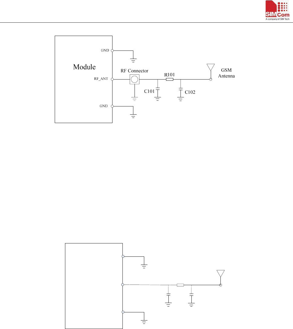
Figure1: GSM antenna matching circuit
R101ˈC101ˈC102 are the matching circuit, the value should be defined by the antenna design. normally R101
is 0, C101 ઼C102 are not SMD. The RF connector is used for conducted
5.2 Bluetooth antenna interface
The module provides a Bluetooth antenna interface named BT_ANT.
The external antenna must be matched properly to achieve best performance, so the matching circuit is
necessary, the connection is recommended as following figure:
GND
Module
BT_ANT
GND
R201
C201 C202
BT
Antenna
Figure 5: BT antenna matching circuit
R201ˈC201ˈC202 are the matching circuit, the value should be defined by the antenna design. R201 is
recommended as 1.2NH and C202 is 1.5pF, C201 are not SMD.
There are some suggestions to components placing and lying for GSM and Bluetooth RF traces:
zThe RF connector is used for conducted test, so keep it as close as pin RF_ANT;
zAntenna matching circuit should be closed to the antenna;
zKeep the RF traces as 50˗
zThe RF traces should be kept far away from the high frequency signals and strong disturbing source.