Simcom 20170406 Smart Module User Manual
Shanghai Simcom Ltd. Smart Module
UserManual.wiki
>
Simcom
>
20170406 User Manual
>
User Manual
Contents
1.
User Manual
2.
Users Manual
User Manual
Navigation menu
Upload a User Manual
Namespaces
Wiki Guide
HTML
PDF
Info
Views
User Manual
Discussion / Help
Navigation
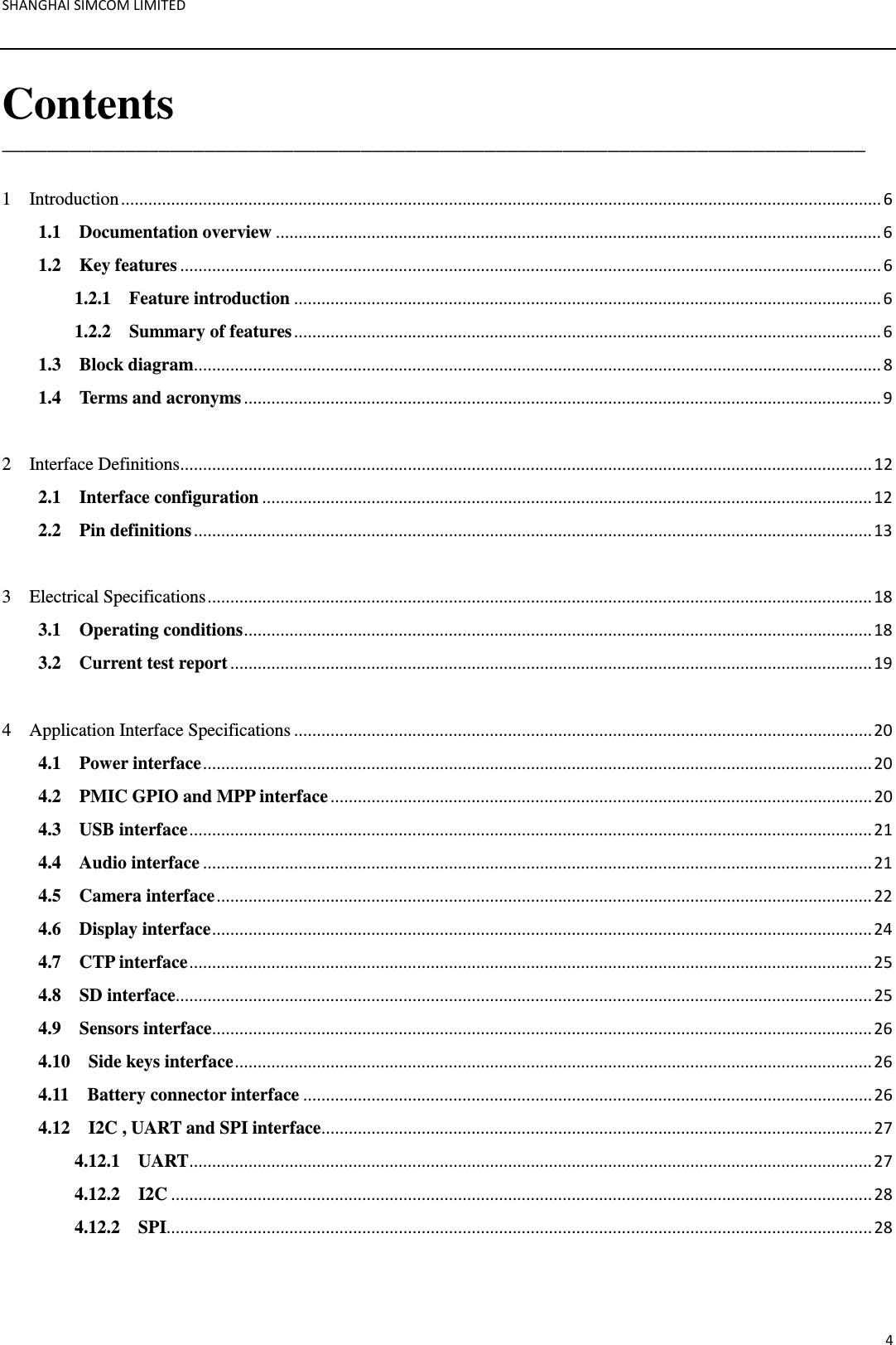
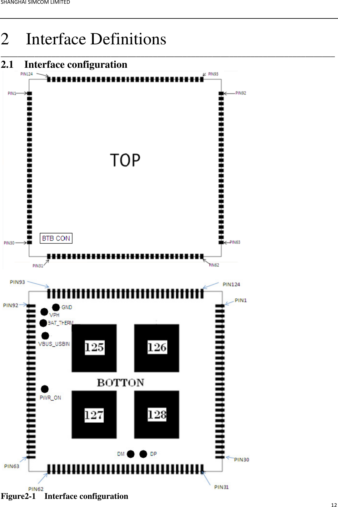
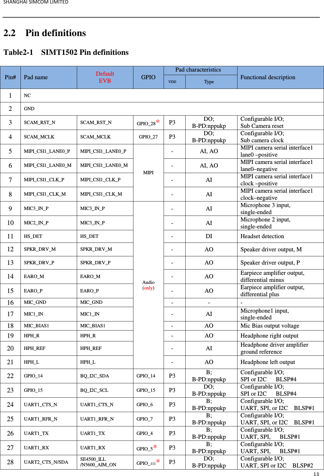
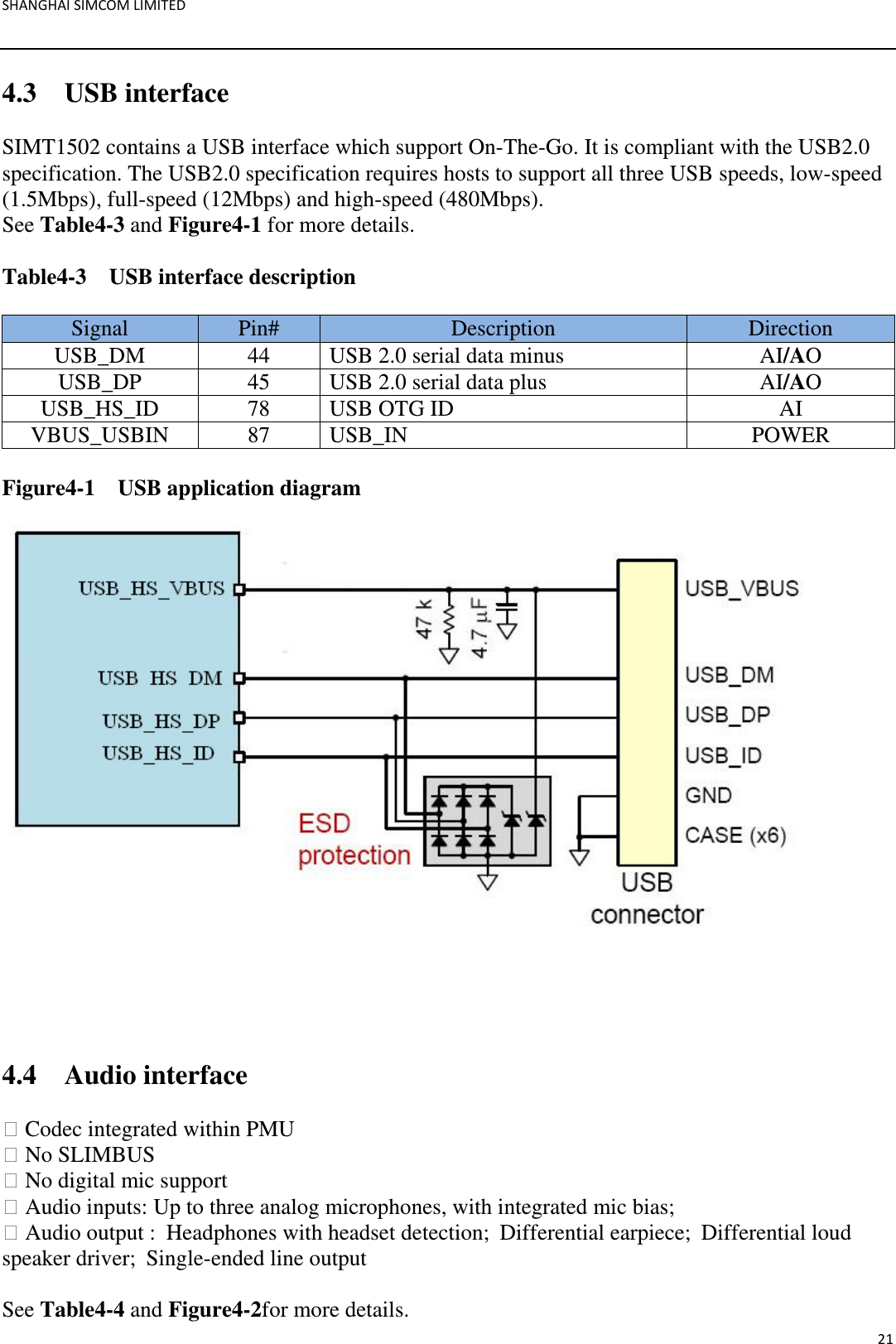
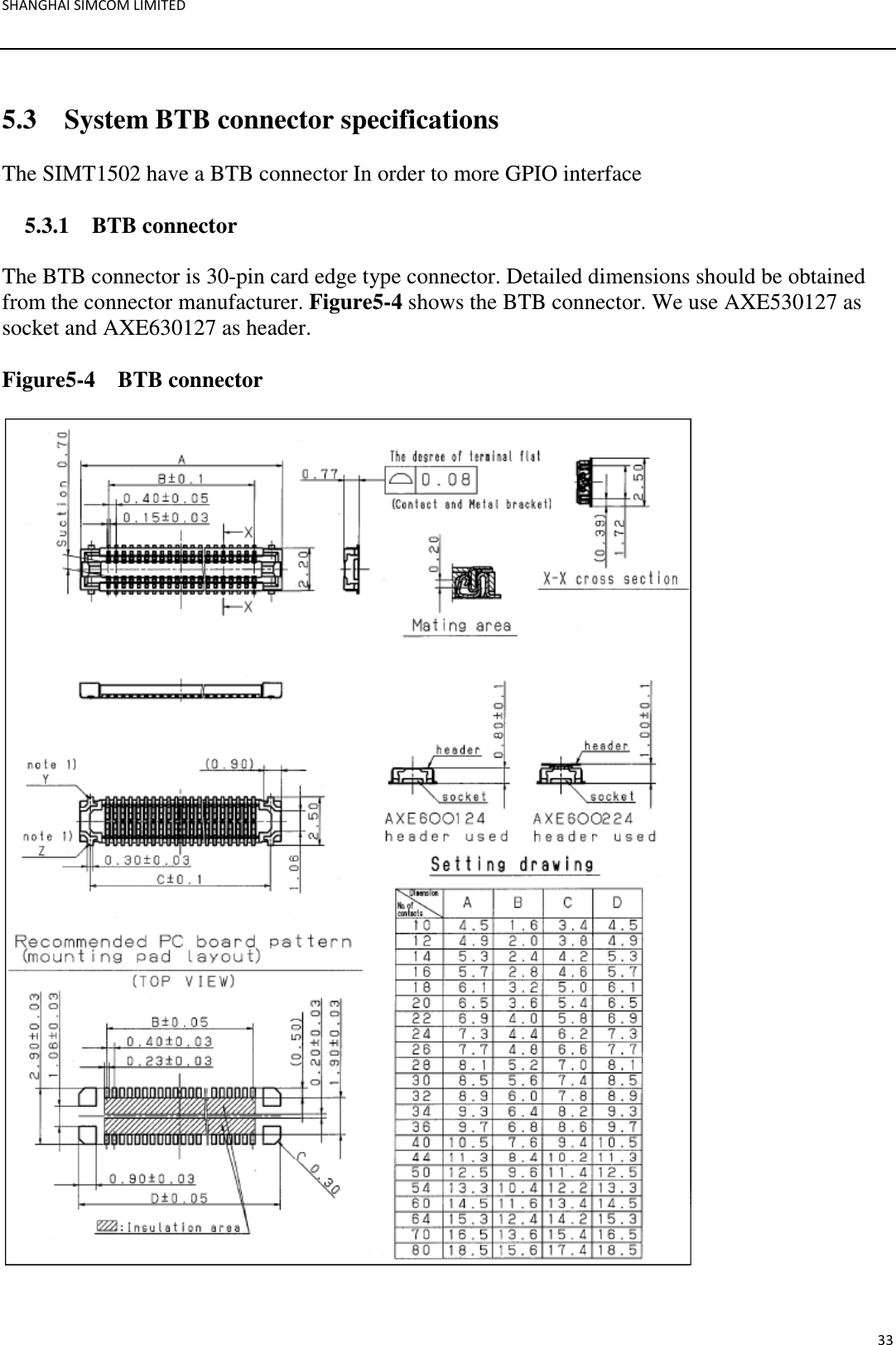
![SHANGHAI SIMCOM LIMITED 8 1.3 Block diagram MAIN BOARDMSM8909WCN3660BPM8909WTR4905MEMORYGPIO28/SCAM_RST_N 3GPIO27/SCAM_MCLK 4MIPI_CSI1_LANE0_P 5MIPI_CSI1_LANE0_N 6MIPI_CSI1_CLK_P 7MIPI_CSI1_CLK_N 8MIC3_IN_P 9 MIC2_IN_P 10CDC_HS_DET 11SPKR_DRV_M 12SPKR_DRV_P 13CDC_EARO_M 14CDC_EARO_P 15MIC_GND 16MIC1_IN_P 17MIC_BIAS1 18CDC_HPH_R 19CDC_HPH_REF 20CDC_HPH_L 21GPIO_14 22GPIO_15 23GPIO_6/UART_CTS_N 24GPIO_7/UART_RFR_N 25GPIO_4/UART_TX 26GPIO_5/UART_RX 27GPIO_111/UART_CTS_N/SDA 28GPIO_112/UART_RFR_N/SCL 29 31 BT_WIFI_INGPIO_13/TS_INT_N 33GPIO_18/TS_12C_SDA 34GPIO_19/TS_12C_SCL 35GPIO_12/TS_RST_N 36GPIO_38/SD_CARD_DET_N 37GPIO_20/UART_TX 38GPIO_21/UART_RX 39GPIO_90/KPSNS0 40GPIO_91/KPSNS1 41GPIO_92/KPSNS2 42USB_DM 44USB_DP 45GPIO_22/AUDIO_PA_EN 47GPIO_28 48GPIO_0/MI2S_WS 49GPIO_1/MI2S_CLK 50GPIO_2/MI2S_D0 51GPIO_3/MI2S_D1 52GPIO_16/ACCEL_INT_1 53SDC2_CMD 54SDC2_DATA0 55SDC2_DATA1 56SDC2_DATA2 57SDC2_DATA3 58SDC2_CLK 5961 VREG_L11_2P95VGPIO_29 63GPIO_52 65666768697071 72 74 75 PM_PWR_ON 7677 PM_VIB_DRV_NUSB_HS_ID 78PMU_MPP_2_PWM 7981 PMU_GPIO01 PM_RES_IN_N 82VREF_BAT_THERM 8485 VREG_L12_2P95V86 GPIO_2487 VBUS_USBIN89 VCOIN BAT_THERM 9092 VPH_PWR93 96 MIPI_DSI0_CLK_P97 MIPI_DSI0_CLK_N98 MIPI_DSI0_LANE3_P99 MIPI_DSI0_LANE3_N100 MIPI_DSI0_LANE2_P101 MIPI_DSI0_LANE2_N102 MIPI_DSI0_LANE1_P103 MIPI_DSI0_LANE1_N104 MIPI_DSI0_LANE0_P105 MIPI_DSI0_LANE0_N106 GPIO_8107 VREG_L17_2P85V108 GPIO_9109 VREG_L6_1P8V110 GPIO_10/CAM_I2C_SDA111 GPIO_11/CAM_I2C_SCL112 GPIO_35/MCAM_RST_N113 GPIO_34/MCAM_STANDBY_N115 MIPI_CSI0_LANE1_N116 MIPI_CSI0_LANE1_P117 MIPI_CSI0_LANE2_P118 MIPI_CSI0_LANE2_N119 MIPI_CSI0_CLK_N120 MIPI_CSI0_CLK_P121 GPIO_33122 GPIO_26/MCAM_CLK124 VPH_PWR2324346626473809195114 123125126127128DEBUGWCNPDET_INWLAN_IOBT/WLAN/FM SSBIBT_STROBEXO_GPM8909RFGPS_RX_I/OCHO_TX_I/OCHO_RX_I/OCHO_GP_DATA SAW LNA SAWJTAGCONNECTORUSBT_FLASHCARDTouchscreenSENSOR:_N;12CMIPI FOR LCM MIPI FOR Main cameraMIPI FOR SUB CAMERACAM_ 12CSDC1EBI0EMMC_NANDLPDDR3AUDIOCXO_EN (BBCLK_EN)CXO_IN (BBCLK 19.2MHz)SLEEP_CLK 32.768KHzRESIN_NPS_HOLDSPMI_CLKSPMI_DATAPMIC_INTRF_CLK1RF_CLK219.2MHzUSBVPH_PWROVPVCHGFET&SNSXO19.2MHzGPIO[0:4]MPP[0:4]BOOST_BYP_BYPUIM_BATT_ALARMENTERN_LDO_CTLGYRO_EN_PMWLED CTL-PWM MODULE OUTPUTHome row (2WLE D * 20mA)PA_THERMVDD_RX_BIAS(1.25V)BTBGND 1GPIO_25 2NC 3NC 4GPIO_31 5GPIO_32 6GPIO_36 7GPIO_58 8GPIO_93 9GPIO_94 10GPIO_95 11GPIO_96 12GPIO_97 13GPIO_110 14GPIO_65 1530 GND29 GND28 GND27 GND26 GND25 GND24 GND23 GND22 GND21 GND20 GND19 GND18 GND17 CND16 GNDGPIO_98 60GPIO_30 6483 PMU_GPIO02 94 SWITCH2.4G5G 30 5G_WIFI88 VBATTR=0ΩOPT1Disable internal ChargingSWITCH COUPLER1 IPEX-3 RF connectorCoaxial line48MHz Figure1-2 SIMT1502 functional block diagram](https://usermanual.wiki/Simcom/20170406.User-Manual/User-Guide-3505317-Page-8.png)