Contents
- 1. User Manual
- 2. Users Manual
User Manual

Smart Module
SIMT 1502
________________________________________________________________
Hardware Version: V1.2
Software Version:CB03_8909_V4.4_20160901
Manufacturer
SHANGHAI SIMCOM LIMITED
Building A,SIM Technology Building,No.633,
Jinzhong
Road,
Changning
District
Expert Importers: Datalogic Srl
Address: Via San Vitalino 13 – 40012 Lippo di Calderara di Reno
SHANGHAI SIMCOM LIMITED
2
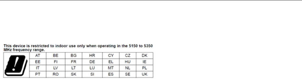
This device is restricted to indoor operation only in the band 5150 - 5350 MHz. (Only
for devices that support 802.11 5 GHz functions)
This device complies with Part 15 of the FCC Rules. Operation is subject to the following two
conditions: (1) this device may not cause harmful interference, and (2) this device must accept any
interference received, including interference that may cause undesired operation.
Changes or modifications not expressly approved by the party responsible for compliance could
void the user’s authority to operate the equipment.
Please notice that if the FCC identification number is not visible when the module is installed
inside another device, then the outside of the device into which the module is installed must also
display a label referring to the enclosed module. This exterior label can use wording such as the
following: “Contains FCC ID: UDV-20170406” any similar wording that expresses the same
meaning may be used.
This equipment complies with FCC radiation exposure limits set forth for an uncontrolled
environment. This equipment should be installed and operated with a minimum distance of 20cm
between the radiator & your body. This transmitter must not be co-located or operating in
conjunction with any other antenna or transmitter.
The module is limited to OEM installation ONLY.
The OEM integrator is responsible for ensuring that the end-user has no manual instruction to
remove or install module.
The module is limited to installation in mobile application;
A separate approval is required for all other operating configurations, including portable
configurations with respect to Part 2.1093 and difference antenna configurations.
There is requirement that the grantee provide guidance to the host manufacturer for compliance
with Part 15B requirements.
This device complies with Industry Canada license-exempt RSS standard(s). Operation is subject
to the following two conditions: (1) this device may not cause interference, and (2) this device
must accept any interference, including interference that may cause undesired operation of the
device.
Le présent appareil est conforme aux CNR d'Industrie Canada applicables aux appareils radio
exempts de licence. L'exploitation est autorisée aux deux conditions suivantes : (1) l'appareil ne
doit pas produire de brouillage, et (2) l'utilisateur de l'appareil doit accepter tout brouillage
radioélectrique subi, même si le brouillage est susceptible d'en compromettre le fonctionnement.
SHANGHAI SIMCOM LIMITED
3
(1)the device for operation in the band 5150-5250 MHz is only for indoor use to reduce the potential for harmful interference to co-channel
mobile satellite systems;
(2)the maximum antenna gain permitted for devices in the bands 5250-5350 MHz and 5470-5725 MHz shall comply with the e.i.r.p. limit; and
(3)the maximum antenna gain permitted for devices in the band 5725-5850 MHz shall comply with the e.i.r.p. limits specified for
point-to-point and non point-to-point operation as appropriate.
(4) Users should also be advised that high-power radars are allocated as primary users (i.e. priority users) of the bands 5250-5350 MHz and
5650-5850 MHz and that these radars could cause interference and/or damage to LE-LAN devices.
(i) les dispositifs fonctionnant dans la bande 5 150-5 250 MHz sont réservés uniquement pour uneutilisation à
l’intérieur afin de réduire les risques de brouillage préjudiciable aux systèmes de satellites mobiles utilisant les
mêmes canaux;
(ii) le gain maximal d’antenne permis pour les dispositifs utilisant les bandes 5 250-5 350 MHz et5 470-5 725 MHz
doit se conformer à la limite de p.i.r.e.;
(iii) le gain maximal d’antenne permis (pour les dispositifs utilisant la bande 5 725-5 850 MHz)
doit se conformer à la limite de p.i.r.e. spécifiée pour l’exploitation point à point et non point à point, selon le
cas.
(iiii) De plus, les utilisateurs devraient aussi être avisés que les utilisateurs de radars de haute puissancesont désignés
utilisateurs principaux (c.-à-d., qu’ils ont la priorité) pour les bandes 5 250-5 350 MHz et 5 650-5 850 MHz et que
ces radars pourraient causer du brouillage et/ou des dommages aux dispositifs LAN-EL.

SHANGHAI SIMCOM LIMITED
4
Contents
_____________________________________________________________________________
1 Introduction ....................................................................................................................................................................... 6
1.1 Documentation overview ..................................................................................................................................... 6
1.2 Key features .......................................................................................................................................................... 6
1.2.1 Feature introduction ................................................................................................................................. 6
1.2.2 Summary of features ................................................................................................................................. 6
1.3 Block diagram ....................................................................................................................................................... 8
1.4 Terms and acronyms ............................................................................................................................................ 9
2 Interface Definitions ........................................................................................................................................................ 12
2.1 Interface configuration ...................................................................................................................................... 12
2.2 Pin definitions ..................................................................................................................................................... 13
3 Electrical Specifications .................................................................................................................................................. 18
3.1 Operating conditions .......................................................................................................................................... 18
3.2 Current test report ............................................................................................................................................. 19
4 Application Interface Specifications ............................................................................................................................... 20
4.1 Power interface ................................................................................................................................................... 20
4.2 PMIC GPIO and MPP interface ....................................................................................................................... 20
4.3 USB interface ...................................................................................................................................................... 21
4.4 Audio interface ................................................................................................................................................... 21
4.5 Camera interface ................................................................................................................................................ 22
4.6 Display interface ................................................................................................................................................. 24
4.7 CTP interface ...................................................................................................................................................... 25
4.8 SD interface ......................................................................................................................................................... 25
4.9 Sensors interface ................................................................................................................................................. 26
4.10 Side keys interface ............................................................................................................................................ 26
4.11 Battery connector interface ............................................................................................................................. 26
4.12 I2C , UART and SPI interface ......................................................................................................................... 27
4.12.1 UART ...................................................................................................................................................... 27
4.12.2 I2C .......................................................................................................................................................... 28
4.12.2 SPI........................................................................................................................................................... 28

SHANGHAI SIMCOM LIMITED
5
4.13 Other interface .................................................................................................................................................. 29
4.13.1 Camera flash Signal .............................................................................................................................. 29
4.13.2 PM_VIB_DRV_N Signal ....................................................................................................................... 29
4.13.3 VCOIN Signal ........................................................................................................................................ 29
4.13.4 RF Signal input port .............................................................................................................................. 30
5 Mechanical Specification ................................................................................................................................................ 31
5.1 Overview ............................................................................................................................................................. 31
5.2 SIMT1502 specifications .................................................................................................................................... 31
5.2.1 SIMT1502 from factor ............................................................................................................................ 31
5.2.2 SIMT1502 PCB details ............................................................................................................................ 32
5.3 System BTB connector specifications ............................................................................................................... 33
5.3.1 BTB connector ......................................................................................................................................... 33
6 RF Specification .............................................................................................................................................................. 34
6.1 R&D parameters ................................................................................................................................................ 33
6.1.1 SIMT1502’s BT&WIFI ........................................................................................................................... 33
6.1.2 SIMT1502 WiFi bands and bandwidth ................................................................................................. 35
6.1.3 SIMT1502 WiFi transmission type and supported Modulation .......................................................... 36
6.1.4 SIMT1502 BT frequency and channels ................................................................................................. 36
6.1.5 SIMT1502 BT transmission type and supported Modulation ............................................................. 36
6.1.6 About how the co-existance between WLAN and BT is managed ...................................................... 36
7 Declaration of Conformity (DoC) ................................................................................................................... 34

SHANGHAI SIMCOM LIMITED
6
1 Introduction
1.1 Documentation overview
This document describes electrical specifications, RF specifications, function interface, mechanical
information and testing conclusions of the SIMT1502. With the help of this document, the users
can easily and quickly use SIMT1502 on their own applications.
1.2 Key features
1.2.1 Feature introduction
SIMT1502 is a very powerful baseband module with 124 pins interface. As a baseband module for
Smartphone/Music player-enabled devices and applications/camera phones/Multimedia phones/
many other terminals,SIMT1502 supports Data-service and many peripheral equipment, which can
be supported by Qualcomm’s ® MSM8909 platform.
1.2.2 Summary of features
SIMT1502 features are listed on the following table (Table1-1)
Table1-1 SIMT1502 features
Feature Capability
Processors
Processors ■ Qualcomm’s® MSM8909:Quad-ARM® Cortex™-A7
application processors up to 1GHz + 512KB L2 cache
■ Modem system: QDSP6 v5 core at up to 691MHz
768 kB L2 caches
■ RPM system :Cortex-M3 for the RPM
Memory support
System memory via EBI ■ 1x LPDDR3 SDRAM: 2GB SDRAM + 16GB EMMC;
32-bit wide; up to 533 MHz
External memory via SDC1 ■ eMMC v4.5/SD flash devices
Multimedia
Display interfaces
■ MIPI_DSI
■ General display features
One
■ 4-lane – 1.5 Gbps per lane; WVGA, up to HD(720p), 60fps
■ Color depth – 24-bit pp(RGB888)
■ Panel types – Most MIPI DSI compliant panels supported;
Camera interfaces
■ Number of CSIs
■ Primary (CSI0)
■ Secondary (CSI1)
■ Configurations supported
■ Two; 1.5 Gbps per lane
■ 2-lane MIPI_CSI0;supports CMOS and CCD sensors
Up to 8MP sensors
■ 1-lane MIPI_CSI1;webcam support 5MP
■ I2C controls

SHANGHAI SIMCOM LIMITED
7
Video applications performance ■Encode: H.264 BP/MP – HD(720p),30 fps
MPEG-4 SP/H.263P0 –WVGA, 30 fps
VP8 – WVGA, 30 fps
■ Encode: H.264 BP/MP/HP – 1080p, 30 fps
MPEG-4 SP/ASP – 1080p, 30 fps
DivX 4x/5x/6x – 1080p, 30 fps
H.263 P0 – WVGA, 30 fps
VP8 – 1080p, 30 fps
(HEVC) H.265 MP 8 bit–1080p, 30 fps
Graphics ■ Adreno™ 304; up to 400 MHz 3D graphics accelerator
Audio
Codec
■ Low-power audio
■ Voice codec support
■ Audio codec support
■ Enhanced audio
■ Synthesizer
Integrated within the MSM8909 device
■ Low power audio for mp3 and AAC playback; surround
sound
■ Versatile – many audio playback & voice modes; encoders
for audio; many concurrency modes
■ G711; Raw PCM; QCELP; EVRC, -B, -WB; AMR-NB,
-WB; GSM-EFR, -FR, -HR;
■ MP3; AAC+, eAAC; AMR-NB, -WB, G.711, WMA 9/10
Pro
■ Dolby Digital Plus and DTS-HD surround
Fluence™ Noise Cancellation;
QAudioFX/Qconcert/QEnsemble;
128-voice polyphony wavetable
Audio inputs ■ Up to 3 analog microphones, with integrated MIC bias
Audio outputs ■ Four outputs : Earpiece Mono AB
Headphones Stereo AB
Speaker 800mW CLASS-D
Connectivity
BLSP ports
■ UART
■ I2C
■ SPI (master only)
6,4 at 4-bits each, 2 at 2-bits each; multiplexed serial interface
functions
■ Yes – two ports up to 4 Mbps
■ Yes – cameras, sensors, NFC, SMB charger, etc.
■ Yes – cameras, sensors, etc.
USB interface ■ One USB 2.0 high-speed
Secure digital interfaces ■ Up to two ports, both dual-voltage
■ One 8-bit and one 4-bit
■ SD 3.0; SD/MMC card; eMMC v4.5
Wireless connectivity
■ WLAN
■ Bluetooth
With WCN3660B
■ WCN3660B : 802.11 a/b/g/n , 2.4G and 5G
■ BT 4.0 LE and earlier
Touch screen support ■ Capacitive panels via external IC (I2C, SPI, & interrupts)
Temperature
Operating Temperature -10 to 60℃
Storage Temperature -30 to 80℃
SHANGHAI SIMCOM LIMITED
8
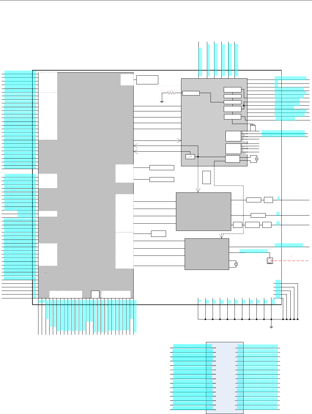
1.3 Block diagram
MAIN BOARD
MSM8909
WCN3660B
PM8909
WTR4905
MEMORY
GPIO28/SCAM_RST_N 3
GPIO27/SCAM_MCLK 4
MIPI_CSI1_LANE0_P 5
MIPI_CSI1_LANE0_N 6
MIPI_CSI1_CLK_P 7
MIPI_CSI1_CLK_N 8
MIC3_IN_P 9
MIC2_IN_P 10
CDC_HS_DET 11
SPKR_DRV_M 12
SPKR_DRV_P 13
CDC_EARO_M 14
CDC_EARO_P 15
MIC_GND 16
MIC1_IN_P 17
MIC_BIAS1 18
CDC_HPH_R 19
CDC_HPH_REF 20
CDC_HPH_L 21
GPIO_14 22
GPIO_15 23
GPIO_6/UART_CTS_N 24
GPIO_7/UART_RFR_N 25
GPIO_4/UART_TX 26
GPIO_5/UART_RX 27
GPIO_111/UART_CTS_N/SDA 28
GPIO_112/UART_RFR_N/SCL 29
31 BT_WIFI_IN
GPIO_13/TS_INT_N 33
GPIO_18/TS_12C_SDA 34
GPIO_19/TS_12C_SCL 35
GPIO_12/TS_RST_N 36
GPIO_38/SD_CARD_DET_N 37
GPIO_20/UART_TX 38
GPIO_21/UART_RX 39
GPIO_90/KPSNS0 40
GPIO_91/KPSNS1 41
GPIO_92/KPSNS2 42
USB_DM 44
USB_DP 45
GPIO_22/AUDIO_PA_EN 47
GPIO_28 48
GPIO_0/MI2S_WS 49
GPIO_1/MI2S_CLK 50
GPIO_2/MI2S_D0 51
GPIO_3/MI2S_D1 52
GPIO_16/ACCEL_INT_1 53
SDC2_CMD 54
SDC2_DATA0 55
SDC2_DATA1 56
SDC2_DATA2 57
SDC2_DATA3 58
SDC2_CLK 59
61 VREG_L11_2P95V
GPIO_29 63
GPIO_52 65
66
67
68
69
70
71
72
74
75
PM_PWR_ON 76
77 PM_VIB_DRV_N
USB_HS_ID 78
PMU_MPP_2_PWM 79
81 PMU_GPIO01
PM_RES_IN_N 82
VREF_BAT_THERM 84
85 VREG_L12_2P95V
86 GPIO_24
87 VBUS_USBIN
89 VCOIN
BAT_THERM 90
92 VPH_PWR
93
96 MIPI_DSI0_CLK_P
97 MIPI_DSI0_CLK_N
98 MIPI_DSI0_LANE3_P
99 MIPI_DSI0_LANE3_N
100 MIPI_DSI0_LANE2_P
101 MIPI_DSI0_LANE2_N
102 MIPI_DSI0_LANE1_P
103 MIPI_DSI0_LANE1_N
104 MIPI_DSI0_LANE0_P
105 MIPI_DSI0_LANE0_N
106 GPIO_8
107 VREG_L17_2P85V
108 GPIO_9
109 VREG_L6_1P8V
110 GPIO_10/CAM_I2C_SDA
111 GPIO_11/CAM_I2C_SCL
112 GPIO_35/MCAM_RST_N
113 GPIO_34/MCAM_STANDBY_N
115 MIPI_CSI0_LANE1_N
116 MIPI_CSI0_LANE1_P
117 MIPI_CSI0_LANE2_P
118 MIPI_CSI0_LANE2_N
119 MIPI_CSI0_CLK_N
120 MIPI_CSI0_CLK_P
121 GPIO_33
122 GPIO_26/MCAM_CLK
124 VPH_PWR
2
32
43
46
62
64
73
80
91
95
114
123
125
126
127
128
DEBUG
WCN
PDET_IN
WLAN_IO
BT/WLAN/FM SSBI
BT_STROBE
XO_G
PM8909
RF
GPS_RX_I/O
CHO_TX_I/O
CHO_RX_I/O
CHO_GP_DATA SAW LNA SAW
JTAG
CONNECTOR
USB
T_FLASH
CARD
Touchscreen
SENSOR:
_N;12C
MIPI FOR LCM MIPI FOR Main
camera
MIPI FOR
SUB
CAMERA
CAM
_ 12C
SDC1
EBI0
EMMC_NAND
LPDDR3
AUDIO
CXO_EN (BBCLK_EN)
CXO_IN (BBCLK 19.2MHz)
SLEEP_CLK 32.768KHz
RESIN_N
PS_HOLD
SPMI_CLK
SPMI_DATA
PMIC_INT
RF_CLK1
RF_CLK2
19.2
MHz
USB
VPH_PWR
OVP
VCHG
FET&SNS
XO
19.2MHz
GPIO
[0:4]
MPP
[0:4]
BOOST_BYP_BYP
UIM_BATT_ALARM
ENTERN_LDO_CTL
GYRO_EN_PM
WLED CTL-PWM MODULE
OUTPUT
Home row (2WLE D * 20mA)
PA_THERM
VDD_RX_BIAS(1.25V)
BTB
GND 1
GPIO_25 2
NC 3
NC 4
GPIO_31 5
GPIO_32 6
GPIO_36 7
GPIO_58 8
GPIO_93 9
GPIO_94 10
GPIO_95 11
GPIO_96 12
GPIO_97 13
GPIO_110 14
GPIO_65 15
30 GND
29 GND
28 GND
27 GND
26 GND
25 GND
24 GND
23 GND
22 GND
21 GND
20 GND
19 GND
18 GND
17 CND
16 GND
GPIO_98 60
GPIO_30 64
83 PMU_GPIO02
94
SWITCH
2.4G
5G
30 5G_WIFI
88 VBATT
R=0Ω
OPT1
Disable internal
Charging
SWITCH COUP
LER
1
IPEX-3 RF
connector
Coaxial line
48MHz
Figure1-2 SIMT1502 functional block diagram

SHANGHAI SIMCOM LIMITED
9
1.4 Terms and acronyms
Table1-2 Terms and acronyms
Term Definition
ADC Analog-to-digital converter
AGC Automatic gain control
AVS Adaptive voltage scaling
BER Bit error rate
BNSP Bare nanoscale packaging
bps Bits per second
BT Bluetooth
CA Carrier aggregation
CDMA Code division multiple access
CRC Cyclic redundancy code
CSI Camera serial interface
CTP Capacitive touch panel
DAC Digital-to-analog converter
DBHSPA Dual-band HSPA
DC-HSPA+ Dual-carrier HSPA+
DCUPA Dual-carrier HSPA
DDR Double data rate
DMB Digital mobile broadcast
DRM Digital Rights Management
DSI Display serial interface
DSP Digital signal processor
EBI External bus interface
EDGE Enhanced data rates for GSM evolution
EDR Enhanced data rate
ETB Embedded trace buffer
QDSS Embedded trace macrocell
EV-DO Evolution data optimized
FDD Frequency division duplex
GNSS Global navigation satellite system
GPIO General-purpose input/output
GPRS General packet radio services
GPS Global positioning system
GPU Graphics processing unit
GRFC Generic RF controller
GSM Global system for mobile communications
HDCP High-bandwidth digital content protection
HSDPA High-speed downlink packet access
HSIC High-speed inter-chip
HSPA+ High-speed packet access

SHANGHAI SIMCOM LIMITED
10
Table1-2 Terms and acronyms (cont.)
Term Definition
HSUPA High-speed uplink packet access
I2C Inter-integrated circuit
I2S Inter-IC sound
ISP Image signal processing
JTAG Joint Test Action Group (ANSI/ICEEE Std. 1149.1-1990)
kbps kilobits per second
LCD Liquid crystal display
LPA Low-power audio
LPASS Low-power audio subsystem
LPDDR Low-power DDR
LSB
Defines whether the LSB is the least significant bit or least significant
byte. All instances of LSB used in this manual are assumed to be LSByte,
unless otherwise specified.
LTE Long term evolution
MBP Mobile broadcast platform
MDM Mobile data modem
MIPI Mobile industry processor interface
MPM Modem power management
MSB
Defines whether the MSB is the most significant bit or most significant
byte. All instances of MSB used in this manual are assumed to be
MSByte, unless otherwise specified.
MTP Modem test platform
NSP Nanoscale package
PA Power amplifier
PCM Pulse-coded modulation
PI Power in
PDM Pulse-density modulation
PM Power management
PNSP Package-on-package nanoscale package
PO Power out
PVS Process voltage scaling
RBDS Radio broadcast data system
RDS Radio data system
RLP Radio link protocol
RPM Resource power manager
SBI Serial bus interface
SD Secure digital
SDC Secure digital controller
SEE Secure Execution Environment
SFS Secure file system
SIM Subscriber identity module
SMT Surface mount technology
SPI Serial peripheral interface

SHANGHAI SIMCOM LIMITED
11
Table1-2 Terms and acronyms (cont.)
Term Definition
SPMI System power management interface
sps Symbols per second (or samples per second)
SPSS Smart peripheral subsystem
SSBI Single-wire SBI
SVS Static voltage scaling
TAP Test access port
TBD To be discussed
TCXO Temperature-compensated crystal oscillator
TDD Time division duplexing
TSIF Transport stream interface
UART Universal asynchronous receiver transmitter
UICC Universal integrated circuit card
UMTS Universal mobile telecommunications system
USB Universal serial bus
USIM UMTS subscriber identity module
WCDMA Wideband code division multiple access
WCN Wireless connectivity network
WLAN Wireless local area network
WTR Wafer-scale RF transceiver
XO Crystal oscillator
ZIF Zero intermediate frequency
SHANGHAI SIMCOM LIMITED
12
2 Interface Definitions
_______________________________________________________________________________
2.1 Interface configuration
Figure2-1 Interface configuration

SHANGHAI SIMCOM LIMITED
13
2.2 Pin definitions
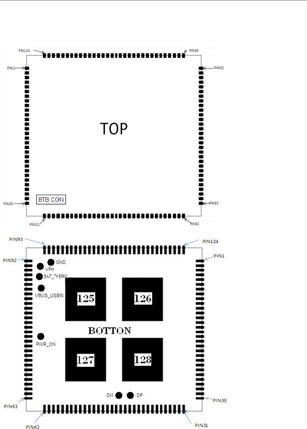
Table2-1 SIMT1502 Pin definitions
Pin#
Pad name Default
EVB GPIO
Pad characteristics
Functional description
VDD Type
1 NC
2 GND
3 SCAM_RST_N SCAM_RST_N GPIO_28*
P3 DO;
B-PD:nppukp
Configurable I/O;
Sub Camera reset
4 SCAM_MCLK SCAM_MCLK GPIO_27 P3 DO;
B-PD:nppukp
Configurable I/O;
Sub camera clock
5 MIPI_CSI1_LANE0_P MIPI_CSI1_LANE0_P
MIPI
- AI, AO MIPI camera serial interface1
lane0 –positive
6 MIPI_CSI1_LANE0_M MIPI_CSI1_LANE0_M - AI, AO MIPI camera serial interface1
lane0–negative
7 MIPI_CSI1_CLK_P MIPI_CSI1_CLK_P - AI MIPI camera serial interface1
clock –positive
8 MIPI_CSI1_CLK_M MIPI_CSI1_CLK_M - AI MIPI camera serial interface1
clock–negative
9 MIC3_IN_P MIC3_IN_P
Audio
(only)
- AI Microphone 3 input,
single-ended
10 MIC2_IN_P MIC3_IN_P - AI Microphone 2 input,
single-ended
11 HS_DET HS_DET - DI Headset detection
12 SPKR_DRV_M SPKR_DRV_M - AO Speaker driver output, M
13 SPKR_DRV_P SPKR_DRV_P - AO Speaker driver output, P
14 EARO_M EARO_M - AO Earpiece amplifier output,
differential minus
15 EARO_P EARO_P - AO Earpiece amplifier output,
differential plus
16 MIC_GND MIC_GND - - -
17 MIC1_IN MIC1_IN - AI Microphone1 input,
single-ended
18 MIC_BIAS1 MIC_BIAS1 - AO Mic Bias output voltage
19 HPH_R HPH_R - AO Headphone right output
20 HPH_REF HPH_REF - AI Headphone driver amplifier
ground reference
21 HPH_L HPH_L - AO Headphone left output
22 GPIO_14 BQ_I2C_SDA GPIO_14 P3 B;
B-PD:nppukp
Configurable I/O;
SPI or I2C BLSP#4
23 GPIO_15 BQ_I2C_SCL GPIO_15 P3 DO;
B-PD:nppukp
Configurable I/O;
SPI or I2C BLSP#4
24 UART1_CTS_N UART1_CTS_N GPIO_6 P3 B;
B-PD:nppukp
Configurable I/O;
UART, SPI, or I2C BLSP#1
25 UART1_RFR_N UART1_RFR_N GPIO_7 P3 B;
B-PD:nppukp
Configurable I/O;
UART, SPI, or I2C BLSP#1
26 UART1_TX UART1_TX GPIO_4 P3 B;
B-PD:nppukp
Configurable I/O;
UART, SPI, BLSP#1
27 UART1_RX UART1_RX GPIO_5* P3 B;
B-PD:nppukp
Configurable I/O;
UART, SPI, BLSP#1
28 UART2_CTS_N/SDA SE4500_ILL
/N5600_AIM_ON GPIO_111*
P3 DO;
B-PD:nppukp
Configurable I/O;
UART, SPI or I2C BLSP#2

SHANGHAI SIMCOM LIMITED
14
29 UART2_CTS_N/SCL SE955_TRIGGER
/N5600_ILL GPIO_112*
P3 DO;
B-PD:nppukp
Configurable I/O;
UART, SPI or I2C BLSP#2
30 NC
31 WIFI_BT_RF WIFI_BT_RF - - AI 2.4G WIFI signal
32 GND
33 TS_IN_N TS_IN_N GPIO_13*
P3 DI;
B-PD:nppukp
Configurable I/O;
Touch screen interrupt
34 TS_I2C_SDA TS_I2C_SDA GPIO_18 P3 B;
B-PD:nppukp
Configurable I/O;
Touch screen I2C
35 TS_I2C_SCL TS_I2C_SCL GPIO_19 P3 DO;
B-PD:nppukp
Configurable I/O;
Touch screen I2C
36 TS_RST_N TS_RST_N GPIO_12*
P3 DO;
B-PD:nppukp
Configurable I/O;
Touch screen reset
37 SD_CARD_DET_N MIPI_SW_EN GPIO_38*
P3 DO;
B-PD:nppukp
Configurable I/O;
Secure digital card detection
38 UART2_TX UART2_TX GPIO_20*
P3 B;
B-PD:nppukp
Configurable I/O;
UART,SPI BLSP#2
39 UART2_RX UART2_RX GPIO_21*
P3 B;
B-PD:nppukp
Configurable I/O;
UART,SPI BLSP#2
40 KYPD_SNS0 KYPD_SNS0 GPIO_90*
P3 DI;
B-PD:nppukp
Keypad sense bit 0;
Configurable I/O
41 KYPD_SNS1 KYPD_SNS1 GPIO_91*
P3 DI;
B-PD:nppukp
Keypad sense bit 1;
Configurable I/O
42 KYPD_SNS2 / KYPD_INT GPIO_92*
P3 DI;
B-PD:nppukp
Keypad sense bit 2;
Configurable I/O
43 GND
44 USB_DM USB_DM
USB - AI, AO USB data – minus
45 USB_DP USB_DP - AI, AO USB data – plus
46 GND
47 AUDIO_PA_EN OTG_PSEL GPIO_22 P3 DO;
B-PD:nppukp Configurable I/O
48 GPIO23 RS232_UART_SEL GPIO_23 P3 DO;
B-PD:nppukp Configurable I/O
49 MI2S_WS SE955_CTS
/N5600_PWR GPIO_0 P3 DI;
B-PD:nppukp
Configurable I/O; SPI;
MI2S #2 word select (L/R)
50 MI2S_SCK SE955_RFR
/N5600_RST GPIO_1 P3 DI;
B-PD:nppukp
Configurable I/O; SPI;
MI2S #2 bit clock
51 MI2S_D0 RS232_EN GPIO_2 P3 DO;
B-PD:nppukp
Configurable I/O; SPI;
MI2S #2 serial data channel 0
52 MI2S_D1 USB_RST
/GP_OUT GPIO_3 P3 DI;
B-PD:nppukp
Configurable I/O; SPI;
MI2S #2 serial data channel 1
53 ACCEL_INT1 SE955_UART_SEL GPIO_16 P3 DO;
B-PD:nppukp
Configurable I/O;
Accelerometer interrupt 1
54 SDC2_CMD SDC2_CMD
SD
(only)
P2 BH-PD:nppukp Secure digital controller 2
command
55 SDC2_DATA_0 SDC2_DATA_0 P2 BH-PD:nppukp Secure digital controller 2
data bit 0
56 SDC2_DATA_1 SDC2_DATA_1 P2 BH-PD:nppukp Secure digital controller 2
data bit 1
57 SDC2_DATA_2 SDC2_DATA_2 P2 BH-PD:nppukp Secure digital controller 2
data bit 2
58 SDC2_DATA_3 SDC2_DATA_3 P2 BH-PD:nppukp Secure digital controller 2
data bit 3
59 SDC2_CLK SDC2_CLK P2 BH-NP:pdpukp Secure digital controller 2
clock
60 MI2S_2_MCLK SCAN_KEY GPIO_98*
P3 DI;
B-PD:nppukp Configurable I/O
61 VREG_L11_2P95V VREG_L11_SDC POWER - PO PMIC output for SDC (only)

SHANGHAI SIMCOM LIMITED
15
62 GND
63 GPIO_29 CAM_I2C_SDA GPIO_29 P3 B;
B-PD:nppukp Camera I2C SDA (only)
64 GPIO_30 CAM_I2C_SCL GPIO_30 P3 DO;
B-PD:nppukp Camera I2C SCL (only)
65 UIM2_PRESENT KYPD_EN GPIO_52 P3 DO;
B-PD:nppukp Configurable I/O;
66
NC
67
68
69
70
71
72
73 GND
74 NC
75
76 PM_KYPD_PWR_N PM_KYPD_PWR_N PMU CTR
- DI Power on key (only)
77 PM_VIB_DRV_N PM_VIB_DRV_N PMU CTR
- PO Vibration motor
driver output control
78 USB_HS_ID USB_HS_ID_MAIN USB - AI USB OTG ID
79 PMU_MPP_2_PWM PWM_OUT PMU CTR
- DO
Configurable I/O;
LED current sink;
LCM PWM
80 GND
81 PMU_GPIO01 NFC_ENABLE PMU
GPIO1 - DO-Z;DI Configurable GPIO;
82 PM_RESIN_N PM_RESIN_N PMU CTR
- DI PMIC reset (only)
83 PMU_GPIO02 NFC_1P8V_EN PMU
GPIO2 - DO-Z;DI Configurable GPIO;
84 VREF_BAT_THERM VREF_BAT_THERM PMU CTR
- AO Reference voltage for battery
thermistor
85 VREG_L12_2P95V VREG_L12_SDC POWER - PO PMIC output for SDC (only)
86 GPIO_24 LCD_TE0 GPIO_24 P3 DI;
B-PD:nppukp Configurable I/O
87 VBUS_USBIN VBUS_USBIN POWER PI USB Voltage
88 VBAT VBATT BAT SNS AI Battery SNS
89 VCOIN VCOIN POWER AI;AO RTC
90 BAT_THERM BAT_THERM - AI Battery therm monitor
91 GND
92 VBAT/VPH VPH_PWR POWER SYS Power
93 NC
94 NC
95 GND
96 MIPI_DSI0_CLK_P MIPI_DSI0_CLK_P
MIPI
AO MIPI display serial interface0
clock – positive
97 MIPI_DSI0_CLK_M MIPI_DSI0_CLK_M AO MIPI display serial interface 0
clock – negative
98 MIPI_DSI0_LANE3_P MIPI_DSI0_LANE3_P AI, AO MIPI display serial interface 0
lane 3 – positive
99 MIPI_DSI0_ LANE3_M
MIPI_DSI0_ LANE3_M
AI, AO MIPI display serial interface 0
lane 3 – negative
100
MIPI_DSI0_ LANE 2_P
MIPI_DSI0_ LANE 2_P
AI, AO MIPI display serial interface 0
lane 2 – positive
101
MIPI_DSI0_ LANE2_M
MIPI_DSI0_ LANE2_M
AI, AO MIPI display serial interface 0
lane 2 – negative

SHANGHAI SIMCOM LIMITED
16
102
MIPI_DSI0_ LANE1_P MIPI_DSI0_ LANE1_P
MIPI
AI, AO MIPI display serial interface 0
lane 1 – positive
103
MIPI_DSI0_ LANE1_M
MIPI_DSI0_ LANE1_M
AI, AO MIPI display serial interface 0
lane 1 – negative
104
MIPI_DSI0_ LANE0_P MIPI_DSI0_ LANE0_P AI, AO MIPI display serial interface 0
lane 0 – positive
105
MIPI_DSI0_ LANE0_M
MIPI_DSI0_ LANE0_M
AI, AO MIPI display serial interface 0
lane 0 – negative
106
GPIO_8 LCD_RST_N GPIO_8 DO;
B-PD:nppukp Configurable I/O
107
VREG_L17_2P85V VREG_L17_2P85V POWER PO PMIC output
108
GPIO_9 CAM_FLASH_EN GPIO_9 DO;
B-PD:nppukp General-purpose wakeup
109
VREG_L6_1P8V VREG_L6_1P8V POWER PO PMIC output
110
CCI_I2C_SDA I2C_SDA GPIO_10 B;
B-PD:nppukp
Configurable I/O;
I2C
111
CCI_I2C_SCL I2C_SCL GPIO_11*
DO;
B-PD:nppukp
Configurable I/O;
I2C
112
MCAM_RST_N MCAM_RST_N GPIO_35*
DO;
B-PD:nppukp
Configurable I/O;
Main Camera reset;
113
MCAM_STANDBY_N MCAM_STANDBY_N GPIO_34*
DO;
B-PD:nppukp
Configurable I/O;
Main Camera standby
114
GND
115
MIPI_CSI0_LANE1_M MIPI_CSI0_LANE1_M
MIPI
AI, AO MIPI camera serial interface 0
lane 1 – negative
116
MIPI_CSI0_ LANE1_P MIPI_CSI0_ LANE1_P AI, AO MIPI camera serial interface 0
lane 1 – positive
117
MIPI_CSI0_ LANE2_P MIPI_CSI0_ LANE2_P AI, AO MIPI camera serial interface 0
lane 2 – positive
118
MIPI_CSI0_ LANE2_M
MIPI_CSI0_ LANE2_M
AI, AO MIPI camera serial interface 0
lane 2 – negative
119
MIPI_CSI0_CLK_M MIPI_CSI0_CLK_M AI MIPI camera serial interface 0
CLK – negative
120
MIPI_CSI0_CLK_P MIPI_CSI0_CLK_P AI MIPI camera serial interface 0
CLK – positive
121
GPIO_33 SCAM_PWDN GPIO_33 DO;
B-PD:nppukp Sub Camera PWND
122
MCAM_MCLK MCAM_MCLK GPIO_26 DO;
B-PD:nppukp Main Camera clock
123
GND GND GND
124
VBAT/VPH VPH_PWR POWER SYS Power
Table2-2 SIMT1502 BTB connector pin definitions
Pin#
Pad name Default
EVB GPIO Pad characteristics Functional description
Voltage Type
1 GND
2 GPIO_25 USB_SW_EN GPIO_25*
P3 DO;
B-PD:nppukp Configurable I/O
3 NC
4 NC
5 GPIO_31 / TC358746_RST GPIO_31*
P3 DO;
B-PD:nppukp Configurable I/O
6 GPIO_32 REFCLK GPIO_32 P3 DO;
B-PD:nppukp Configurable I/O
7 GPIO_36 CHG_INT GPIO_36*
P3 DI;
B-PD:nppukp Configurable I/O
8 GPIO_58 GYRO_INT_EN GPIO_58*
P3 DO;
B-PD:nppukp Configurable I/O

SHANGHAI SIMCOM LIMITED
17
9 GPIO_93 OTG_EN GPIO_93 P3 DO;
BB-PD:nppukp Configurable I/O
10 GPIO_94 ALSP_INT_N GPIO_94*
P3 DI;
BB-PD:nppukp Configurable I/O
11 GPIO_95 CHG_EN GPIO_95*
P3 DO;
BB-PD:nppukp Configurable I/O
12 GPIO_96 VBUS_OTG_EN GPIO_96*
P3 DO;
BB-PD:nppukp Configurable I/O
13 GPIO_97 NFC_DWL_REQ GPIO_97*
P3 DI;
B-PD:nppukp Configurable I/O
14 GPIO_110 NFC_INT_N GPIO_110*
P3 DI;
B-PD:nppukp Configurable I/O
15 GPIO_65 MAG_RESET GPIO_65*
P3 DI;
B-PD:nppukp Configurable I/O
16 GND
17 GND
18 GND
19 GND
20 GND
21 GND
22 GND
23 GND
24 GND
25 GND
26 GND
27 GND
28 GND
29 GND
30 GND
NOTE:I/O parameter definitions
Symbol
* General purpose wakeup
AI Analog input
AO Analog output
B Bidirectional digital with CMOS input
CSI Supply voltage for MIPI_CSI circuits and I/Os; tied to VDD_MIPI_CSI (1.8 V only)
DI Digital input(CMOS)
DO Digital output(CMOS)
DSI Supply voltage for MIPI_DSI I/Os; tied to VDD_QFPROM_PRG (1.8 V only)
H High-voltage tolerant
KP Contains an internal weak keeper device (keepers cannot drive external buses)
NP Contains no internal pull
PD Contains an internal pulldown device
PU Contains an internal pullup device
PI Power input
PO Power output
V_G
Selectable supply for GPIO circuits; options include:
VIN0: 3.6 V VIN1: 3.075 V
VIN2: 1.2 V VIN3: 1.8 V
V_INT Internally generated voltage supply voltage for some power on circuits
Z High-impedance (high-Z) output
SHANGHAI SIMCOM LIMITED
18
3 Electrical Specifications
_______________________________________________________________________________
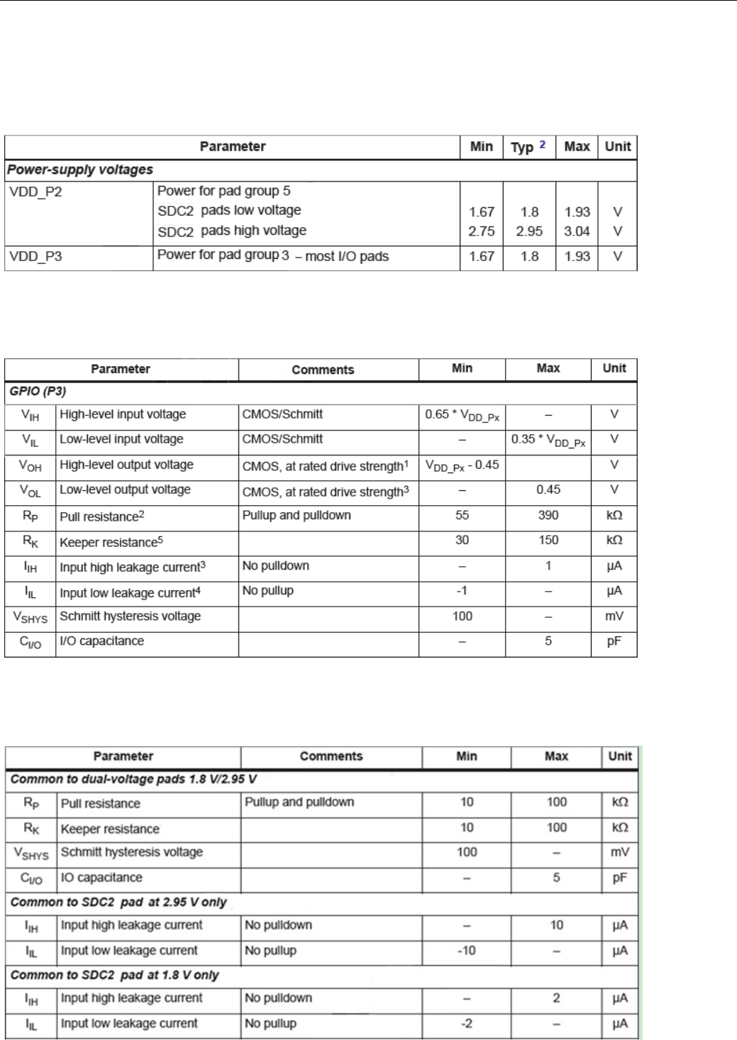
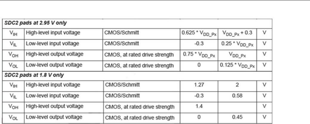
3.1 Operating conditions
1.8 V digital I/O characteristics
1.8 V digital I/O characteristics1.8 V digital I/O characteristics
1.8 V digital I/O characteristics
(
((
(P3)
))
):
::
:
VDD_P3GPIOs
Dual
DualDual
Dual-
--
-voltage 1.8 V/2.95 V digital I/O characteristics
voltage 1.8 V/2.95 V digital I/O characteristicsvoltage 1.8 V/2.95 V digital I/O characteristics
voltage 1.8 V/2.95 V digital I/O characteristics
:
::
:
VDD_P2SDC2
SHANGHAI SIMCOM LIMITED
19
3.2 Current test report
This Current test report based on the EVB board, Vbat=3.8V. All values are typical unless
otherwise specified.
1. During suspend (Airplane mode, no UIM, system in sleep mode): 2.9mA.
2. During suspend (WIFI wake up, BT off, system in sleep mode): 3.0mA.
3. Module power off (Do not remove the battery): 75uA(Without Vcoin); 250uA(With Vcoin).
SHANGHAI SIMCOM LIMITED
20
4 Application Interface Specifications
_______________________________________________________________________________
4.1 Power interface
The power supply of SIMT1502 comes from PM8909. See Table4-1
Table4-1 Power source description
Signal Pin# Direction
Voltage(V) Current(mA)
PI/PO Min Typ Max Max
VREG_L11_2P95V 61 PO 1.75 2.95 3.337 600
VREG_L12_2P95V 85 PO 1.75 1.8/2.95
3.337 50
VREG_L17_2P85V 107 PO 1.75 2.85 3.337 420
VREG_L6_1P8V 109 PO 1.75 1.8 3.337 200
Signal Pin# Direction
Functions
PI/PO
VBAT_SNS 88 PI Battery SNS
VBAT/VPH 92 PI/PO SYS Power
VBAT/VPH 124 PI/PO SYS Power
VBAT means battery, VPH means SYS Power. If you use the SIMT1502’s internal charging
management, they are the same function and they must be connected together. If you use external
charging management, PIN88 is Battery only and PIN92/124 is VPH only. You can see it in
SIMT1502_HW_compatibility design of the modification.pdf document.
4.2 PMIC GPIO and MPP interface
SIMT1502 have two PMIC GPIO interface and one PMIC Multipurpose interface.See Table4-2.
Table4-2 PMIC GPIO and MPP interface description
GPIO/MPP Pin# Functions
PMU_GPIO01 81 RFCLK1_EN
PMU_GPIO02 83 RFCLK2_EN
PMU_MPP_2_PWM 79 PWM output
Two GPIOs are available. Some likely GPIO applications, which are described elsewhere: clock
outputs; external current driver control; external LDO, SMPS, or power gate controls; status bit;
XO controller input; and level translator.
One MPP are available. MPP can be configured as PWM, and MPP can be configured as analog
output buffers.
SHANGHAI SIMCOM LIMITED
21
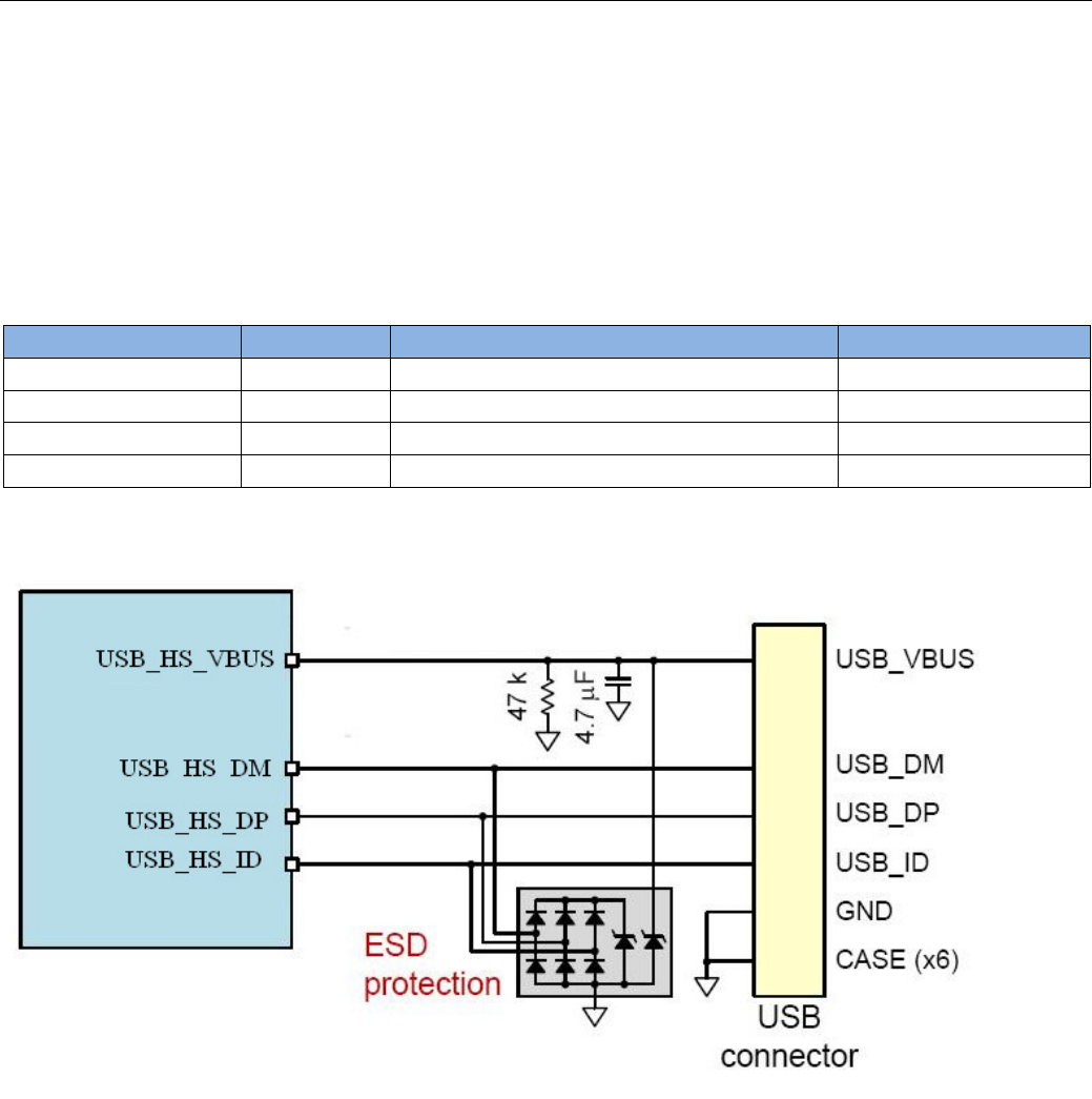
4.3 USB interface
SIMT1502 contains a USB interface which support On-The-Go. It is compliant with the USB2.0
specification. The USB2.0 specification requires hosts to support all three USB speeds, low-speed
(1.5Mbps), full-speed (12Mbps) and high-speed (480Mbps).
See Table4-3 and Figure4-1 for more details.
Table4-3 USB interface description
Signal Pin# Description Direction
USB_DM 44 USB 2.0 serial data minus AI
/
A
O
USB_DP 45 USB 2.0 serial data plus AI
/
A
O
USB_HS_ID 78 USB OTG ID AI
VBUS_USBIN 87 USB_IN POWER
Figure4-1 USB application diagram
4.4 Audio interface
Codec integrated within PMU
No SLIMBUS
No digital mic support
Audio inputs: Up to three analog microphones, with integrated mic bias;
Audio output : Headphones with headset detection; Differential earpiece; Differential loud
speaker driver; Single-ended line output
See Table4-4 and Figure4-2for more details.
SHANGHAI SIMCOM LIMITED
22
Table4-4 Audio interface description
Signal Pin# Description Direction
AI
/A
O
MIC3_IN 9 Microphone 3 input, single-ended AI
MIC2_IN 10 Microphone 2 input, single-ended AI
HS_DET 11 Headset detection AI
SPKR_DRV_M 12 Speaker driver output, minus AO
SPKR_DRV_P 13 Speaker driver output, plus AO
EARO_M 14 Earpiece amplifier output, differential minus AO
EARO_P 15 Earpiece amplifier output, differential plus AO
MIC_GND 16 GND GND
MIC1_IN 17 Microphone 1 input, single-ended AI
MIC_BIAS 18 Microphone bias output voltage AO
HPH_R 19 Headphone right output AO
HPH_REF 20 Headphone driver amplifier ground reference AI
HPH_L 21 Headphone left output AO
Figure4-2 Audio application diagram
4.5 Camera interface
SIMT1502 contains two camera interface. Primary camera interface use 2-lane MIPI_CSI0,
supports CMOS and CCD sensors, up to 8MP sensors. Secondary camera interface use 1-lane
MIPI_CSI1, and 1.5Gbps per lane. Both are controlled by I2C bus.
See Table4-5 and Figure4-3for more details.
Table4-5 Camera interface description
Signal Pin# Description Direction
AI
/A
O
SCAM_RST_N 3 Camera0 (front camera) reset DO
SCAM_MCLK1 4 Camera0 master clock 1 DO
MIPI_CSI1_LN0_P 5 MIPI camera serial interface 1 lane 0 – positive AI
,A
O
MIPI_CSI1_LN0_N 6 MIPI camera serial interface 1 lane 0 – negative
AI, AO
SHANGHAI SIMCOM LIMITED
23
MIPI_CSI1_CLK_P 7 MIPI camera serial interface 1 clock – positive AI
MIPI_CSI1_CLK_N 8 MIPI camera serial interface 1 clock – negative AI
CAM_PWDN 121 Camera0 PWDN DO
CAM_I2C_SDA 63 Camera I2C,SDA B
CAM_I2C_SCL 64 Camera I2C,SCL DO
CAM1_RST_N 112 Camera 1 (rear camera) reset DO
CAM1_STANDBY_N 113 Camera 1 (rear camera) standby DO
MIPI_CSI0_LN1_N 115 MIPI camera serial interface 0 clock – negative AI
,A
O
MIPI_CSI0_LN1_P 116 MIPI camera serial interface 0 clock – positive AI
,A
O
MIPI_CSI0_LN2_P 117 MIPI camera serial interface 0 lane 2 – positive AI
,A
O
MIPI_CSI0_LN2_N 118 MIPI camera serial interface 0 lane 2 – negative
AI
,A
O
MIPI_CSI0_CLK_N 119 MIPI camera serial interface 0 clock – negative AI
MIPI_CSI0_CLK_P 120 MIPI camera serial interface 0 clock – positive AI
CAM_MCLK0 122 Camera1 master clock 0 DO
Figure4-3 CSI application diagram
Normally, camera need 2.85V and 1.8V voltage, we can use external LDO to replace
VREG_L6_1P8 and VERG_L17_2P85.At the same time, if the rear camera have AF
function, another external LDO is necessary.
SHANGHAI SIMCOM LIMITED
24
4.6 Display interface
SIMT1502 contains one display interface. The interface use MIPI display serial interface, support
up to four lanes. Support for the resolution of WVGA, qHD and 720p LCM..
The backlight circuit is not contained in SIMT1502, which must be designed in external circuit.
See Table4-6 and Figure4-4for more details.
Table4-6 Display interface description
Signal Pin# Description Direction
AI
/A
O
DSI_LCD_TE0 86 LCD data write sync signal DO
PMU_MPP3_WM 79 PWM DO
MIPI_DSI_CLK_P 96 MIPI display serial interface 0 clock – positive AO
MIPI_DSI_CLK_N 97 MIPI display serial interface 0 clock – negative AO
MIPI_DSI_LN3_P 98 MIPI display serial interface 0 lane 3 – positive AI
,A
O
MIPI_DSI_LN3_N 99 MIPI display serial interface 0 lane 3 –negative AI
,A
O
MIPI_DSI_LN2_P 100 MIPI display serial interface 0 lane 2 – positive AI
,A
O
MIPI_DSI_LN2_N 101 MIPI display serial interface 0 lane 2 – negative AI
,A
O
MIPI_DSI_LN1_P 102 MIPI display serial interface 0 lane 1 – positive AI
,A
O
MIPI_DSI_LN1_N 103 MIPI display serial interface 0 lane 1 – negative AI
,A
O
MIPI_DSI_LN0_P 104 MIPI display serial interface 0 lane 0 – positive AI
,A
O
MIPI_DSI_LN0_N 105 MIPI display serial interface 0 lane 0 – negative AI
,A
O
LCD_ID 106 LCD ID pin DI
DSI_RST_N 108 General-purpose wakeup DO
Figure4-4 Display application diagram
SHANGHAI SIMCOM LIMITED
25
4.7 CTP interface
SIMT1502 contains one CTP interface, the panel is controlled by I2C bus.
See Table4-7 and Figure4-5 for more details.
Table4-7 CTP interface description
Signal Pin# Description Direction
AI/AO
TS_INT_N 33 Touchscreen interrupt DI
TS_I2C_SDA 34 Touchscreen I2C,SDA B
TS_I2C_SCL 35 Touchscreen I2C,SCL DO
TS_RST_N 36 Touchscreen reset DO
Figure4-5 CTP application diagram
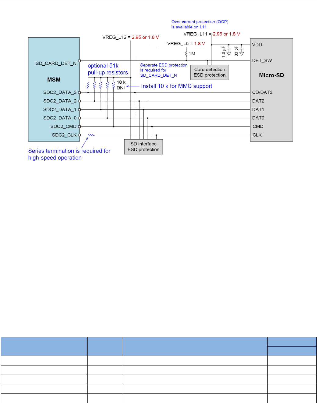
4.8 SD interface
SIMT1502 contains a SD interface, the clock output up to 200MHz,need support 1.8/2.95V
dual-voltage. If SD connector have detect pin, the hot plug function can be done.
See Table4-8 and Figure4-6 for more details.
Table4-8 SD interface description
Signal Pin# Description Direction
AI
/A
O
SD_CARD_DET__N
37 Secure digital card detection DI
SDC2_CMD 54 Secure digital controller 2 command AI,AO
SDC2_DATA_0 55 Secure digital controller 2 data bit 0 AI,AO
SDC2_DATA_1 56 Secure digital controller 2 data bit 1 AI,AO
SDC2_DATA_2 57 Secure digital controller 2 data bit 2 AI,AO
SDC2_DATA_3 58 Secure digital controller 2 data bit 3 AI,AO
SDC2_CLK 59 Secure digital controller 2 clock AI,AO
SHANGHAI SIMCOM LIMITED
26
Figure4-6 SD interface application diagram
4.9 Sensors interface
SIMT1502 support many sensors via I2C bus, the circuit structure is similar to camera interface.
SIMT1502 does not contain necessary pull_up resistors internal, which must be designed in
external circuit.
4.10 Side keys interface
SIMT1502 contains a few keys interfaces, which can be used as functional side keys.
KYPD_SNS0,KYPD_SNS1and KYPD_SNS2 can compose matrix keyboard, also can be used as
normal configurable GPIO.
See Table4-9 for more details.
Table4-9 Side keys interface description
Signal Pin# Description Direction
DI
/
DO
KYPD_SNS0 40 Keypad sense bit 0 DI
KYPD_SNS1 41 Keypad sense bit 1 DI
KYPD_SNS2 42 Keypad sense bit 2 DI
PM_KYPD_PWR_N 76 Power on key DI
PM_RESIN_N 82 PMIC reset input DI
4.11 Battery connector interface
SHANGHAI SIMCOM LIMITED
27
SIMT1502 must be provided voltage by external voltage source.
See Table4-10 for more details.
Table4-10 Battery connector description
Signal Pin# Description Direction
AI
/
AO
BAT_THERM 90 Battery therm monitor AI
VBATT 88/92/124(No External Charging IC) Battery positive supply AI
VBATT 88 (With External Charging IC) Battery positive supply AI
GND 2/32/43/46/62/73/80/91/95/
114/123/125/126/127/128 Ground -
4.12 I2C , UART and SPI interface
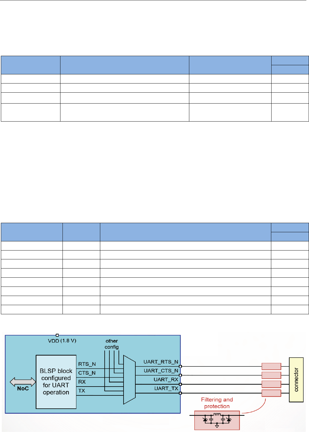
4.12.1 UART
SIMT1502 contains two groups UART_DM .The UART_DM is used to support high-speed
UART operation up to 4 Mbps for debug and system log. UART only supports Slow_IrDA.
See Table4-11 and Figure4-7 for more details:
Table4-11 UART interface description
Signal Pin# Description Direction
I
/
O
GPIO_4 26 UART1 TX O
GPIO_5 27 UART1 RX I
GPIO_6 24 UART1 CTS_N I
GPIO_7 25 UART1 RTS_N O
GPIO_20 38 UART2 TX O
GPIO_21 39 UART2 RX I
GPIO_111 28 UART2 CTS_N I
GPIO_112 29 UART2 RTS_N O
Figure4-7 UART application diagram

SHANGHAI SIMCOM LIMITED
28
4.12.2 I2C
SIMT1502 contains two groups special functional and four groups configurable I2C, which
multiplexed with UART function. I2C pins use GPIOs configured as open-drain outputs; the
pull-up resistor(2.2K) must be provided by external circuit(1.8V).
High speed mode I2C running at 3.4 MHz.
See Table4-12
Table4-12 I2C interface description
Signal Pin# Description Direction
AI/AO
TS_I2C_SDA 34 Touchscreen/ SENSORS I2C,SDA B
TS_I2C_SCL 35 Touchscreen/ SENSORS I2C,SCL DO
CCI_I2C_SDA 63 Camera I2C,SDA B
CCI_I2C_SCL 64 Camera I2C,SCL DO
The rest of I2C interface is multiplexed with UART function.
See Table4-13 for more details.
Table4-13 I2C interface alternate function description
Signal Pin# Alternate function
GPIO_6 24 UART2 CTS_N/GP BLSP#1_I2C_SDA_B
GPIO_7 25 UART2 RTS_N/GP BLSP#1_I2C_SCL_B
GPIO_111 28 UART2 CTS_N/GP BLSP#2_I2C_SDA_B
GPIO_112 29 UART2 RTS_N/GP BLSP#2_I2C_SCL_B
GPIO_14 22 SPI4 CS_N/GP BLSP4#_I2C_SDA_B
GPIO_15 23 SPI4 CLK/GP BLSP4#_I2C_SCL_B
GPIO_10 110 SPI6 CS_N/GP BLSP6#_I2C_SDA_B
GPIO_11 111 SPI6 CLK/GP BLSP6#_I2C_SCL_B
4.12.2 SPI
SIMT1502 contains three groups configurable SPI, which multiplexed with UART/I2C function.
But, SIMT1502 only be used for master device.
See Table4-14
Table4-14 SPI interface alternate function description

SHANGHAI SIMCOM LIMITED
29
Signal Pin# Description Direction
I
/
O
GPIO_4 26 SPI1 MOSI O
GPIO_5 27 SPI1 MISO I
GPIO_6 24 SPI1 CS_N O
GPIO_7 25 SPI1 CLK O
GPIO_20 38 SPI2 MOSI O
GPIO_21 39 SPI2 MISO I
GPIO_111 28 SPI2 CS_N O
GPIO_112 29 SPI2 CLK O
GPIO_0 49 SPI3 MOSI O
GPIO_1 50 SPI3 MISO I
GPIO_2 51 SPI3 CS_N O
GPIO_3 52 SPI3 CLK O
4.13 Other interface
4.13.1 Camera flash Signal
These camera flash signal provide flash and torch mode enable. The FLASH_NOW trigger the
camera flash into torch mode. The FLASH_EN enable the camera flash to flash mode.
4.13.2 PM_VIB_DRV_N Signal
The PM_VIB_DRV_N is used to control vibration intensity. The vibration driver is a
programmable voltage output that is referenced to VDD; when off, its output voltage is VDD. The
motor is connected between VDD and the PM_VIB_DRV_N pin.
See Table4-15
Table4-15 PM_VIB_DRV_N Signal
Signal Pin# Description Direction
I
/
O
PM_VIB_DRV_N 77 Vibration motor driver output control PO
4.13.3 VCOIN Signal
VCOIN requires either a lithium manganese dioxide rechargeable coin cell or a keep-alive
capacitor, so that the appropriate oscillator and real-time clock circuits continue to run when the
phone is off.
See Table4-16
Table4-16 VCOIN Signal
Signal Pin# Description Direction
I
/
O
SHANGHAI SIMCOM LIMITED
30
VCOIN 89 Sense input or charge output AI,AO
4.13.4 RF Signal input port
SIMT1502 contains four RF signal input port: BT/WIFI.
See Table4-16 and Figure4-8 for more details:
Table4-17 RF Signal input port
Signal Pin# Description Direction
I
/
O
RF_IN_2 30 5G_WIFI AI,AO
WIFI_BT_RF 31 BT/WIFI AI,AO
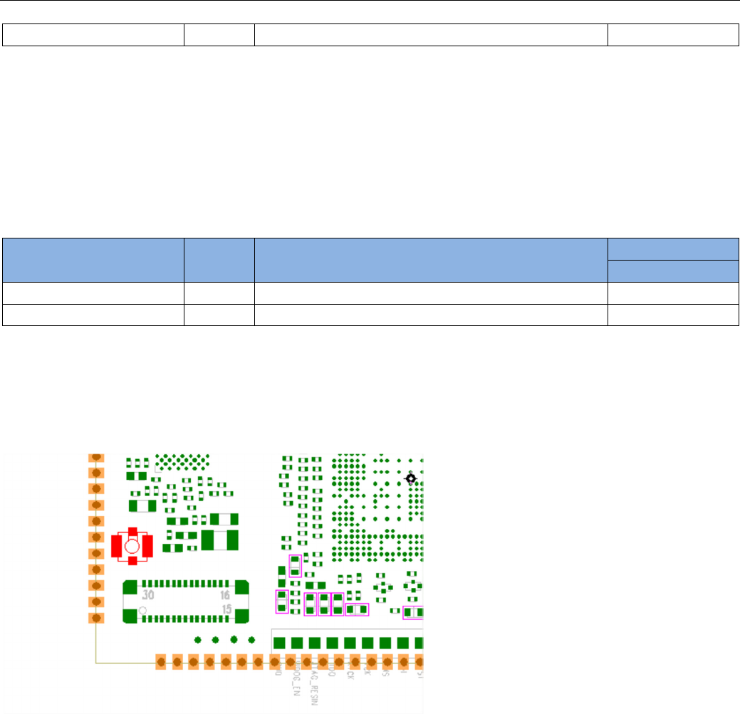
If you want to use 5G_WIFI, you must use the RF Cable Line (IPX-3) connect the RF base, which
close to BTB connect on SIMT1502.See Figure4-8 for more details
Figure4-8 5G_WIFI: Red part
SHANGHAI SIMCOM LIMITED
31
5 Mechanical Specification
_______________________________________________________________________________
5.1 Overview
This specification defines a small form factor module for systems in which a Stamp hole package
add-in module can not be used due to mechanical system design constraints. The specification
defines a smaller module based on a single 124-pin Leadless Chip Carriers encapsulation for
system interfaces by card edge type. The specification also defines the Stamp hole package system.
5.2 SIMT1502 specifications
There is Stamp hole package add-in SIMT1502 size.
For purposes of the drawings in this specification, the following notes apply:
All dimensions are in millimeters, unless otherwise specified.
All dimensions tolerances are ± 0.15 mm, unless otherwise specified.
Dimensions marked with an asterisk (*) are overall envelope dimensions and include space
allowances for insulation to comply with regulatory and safety requirements.
Insulating material shall not interfere with or obstruct mounting holes or grounding pads.
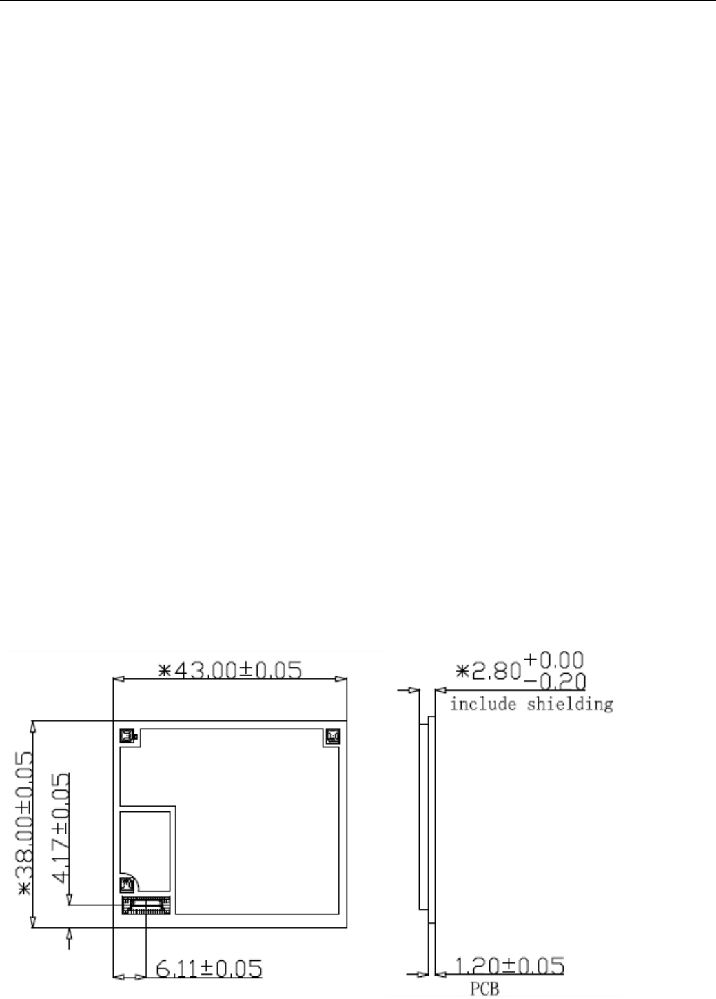
5.2.1 SIMT1502 from factor
The SIMT1502 form factor is specified by Figure5-1.
The figure illustrates a module example application. The hatched area shown in this figure
represents the available component volume for the SIMT1502’s circuitry.
Figure5-1 SIMT1502 form factor
SHANGHAI SIMCOM LIMITED
32
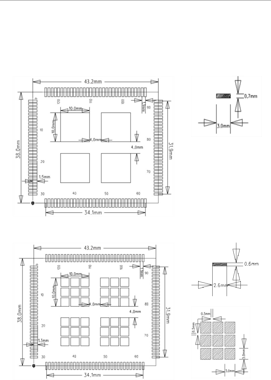
5.2.2 SIMT1502 PCB details
The following figures (Figure5-2) provide the printed circuit board (PCB) details required to
fabricate the PCB. The PCB for this application is expected to be 1.2 mm thick. The steel net
thickness is 0.12mm (Figure5-3).
Figure5-2 SIMT1502 Pads
The dimension tolerance is ± 0.005 mm (±0.2mil).
Figure5-3 SIMT1502 Steel net
The dimension tolerance is ± 0.005 mm (±0.2mil).
SHANGHAI SIMCOM LIMITED
33
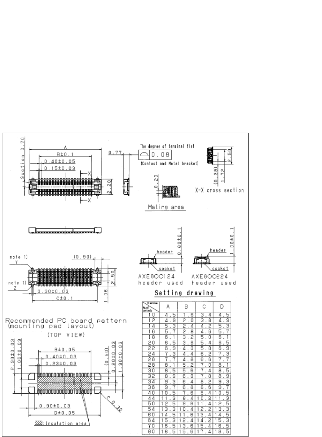
5.3 System BTB connector specifications
The SIMT1502 have a BTB connector In order to more GPIO interface
5.3.1 BTB connector
The BTB connector is 30-pin card edge type connector. Detailed dimensions should be obtained
from the connector manufacturer. Figure5-4 shows the BTB connector. We use AXE530127 as
socket and AXE630127 as header.
Figure5-4 BTB connector

SHANGHAI SIMCOM LIMITED
34
6 RF Specification
_______________________________________________________________________________
6.1 R&D parameters
All measurements are taken at module RF I/O pins (pin 31 for BT/WIFI and RF connector for 5G_WIFI) with
IQ2015. All typical performance specifications are based on operation at room temperature (+25°C) using default
parameter settings and nominal supply voltages, such as VBAT = 3.8V.
6.1.1 SIMT1502’s BT&WIFI
Table6-1 BT&WIFI (For CE)
Item specifications
BT TX Power<10dBm
BLE TX Power<5dBm
WIFI TX Power<22dBm
The sensitivity of 5G WiFi CH36 have separate standards as follow Table6-2 CH36.
Table6-2 CH36
802.11a 6 M <-83dB
54M <-68dB
802.11n
MCS0-HT20 <-83dB
MCS7-HT20 <-66dB
MCS0-HT40 <-83dB
MCS7-HT40 <-64dB
6.1.2 SIMT1502 WiFi bands and bandwidth
The SIMT1502 WiFi bands and bandwidth is specified by Table6-3 and Table6-4.
2.4GHz WiFi only support 20MHz channels bandwidth.
5GHz WiFi can support both 20MHz and 40MHz channels bandwidth.
Table6-3 2.4G WiFi channels
Channel Frequency(MHz)
CHAN1 2412

SHANGHAI SIMCOM LIMITED
35
CHAN2 2417
CHAN3 2422
CHAN4 2427
CHAN5 2432
CHAN6 2437
CHAN7 2442
CHAN8 2447
CHAN9 2452
CHAN10
2457
CHAN11
2462
CHAN12
2467
CHAN13
2472
Table6-4 5G WiFi channels
20MHz 40MHz
Channel
Frequency
Channel
Frequency
CHAN36 5180 CHAN38 5190
CHAN40 5200 CHAN42 5210
CHAN44 5220 CHAN46 5230
CHAN48 5240 CHAN50 5250
CHAN52 5260 CHAN54 5270
CHAN56 5280 CHAN58 5290
CHAN60 5300 CHAN62 5310
CHAN64 5320 CHAN102
5510
CHAN100
5500 CHAN106
5530
CHAN104
5520 CHAN110
5550
CHAN108
5540 CHAN114
5570
CHAN112
5560 CHAN118
5590
CHAN116
5580 CHAN122
5610
CHAN120
5600 CHAN126
5630
CHAN124
5620 CHAN130
5650
CHAN128
5640 CHAN134
5670
CHAN132
5660 CHAN138
5690
CHAN136
5680 CHAN142
5710
CHAN140
5700 CHAN151
5755
CHAN144
5720 CHAN155
5775
CHAN149
5745 CHAN159
5795
CHAN153
5765 CHAN163
5815
CHAN157
5785
CHAN161
5805
CHAN165
5825
6.1.3 SIMT1502 WiFi transmission type and supported Modulation
The SIMT1502 WiFi transmission type and supported Modulation is specified by Table6-5.
Table6-5 WiFi transmission type and supported Modulation

SHANGHAI SIMCOM LIMITED
36
Data Rate(Mbps) Modulation Format
802.11B
1Mbps(DSSS) DBPSK
2Mbps(DSSS) DQPSK
5.5Mbps(CCK) DQPSK
11Mbps(CCK) DQPSK
802.11A / G
6Mbps(OFDM) BPSK
9Mbps(OFDM) BPSK
12Mbps(OFDM) QPSK
18Mbps(OFDM) QPSK
24Mbps(OFDM) 16QAM
36Mbps(OFDM) 16QAM
48Mbps(OFDM) 64QAM
54Mbps(OFDM) 64QAM
802.11N
(HT20)
6.5Mbps(MCS0) BPSK
13Mbps(MCS1) QPSK
19.5Mbps(MCS2) QPSK
26Mbps(MCS3) 16QAM
39Mbps(MCS4) 16QAM
52Mbps(MCS5) 64QAM
58.5Mbps(MCS6) 64QAM
65Mbps(MCS7) 64QAM
802.11N
(HT40)
13.5Mbps(MCS0) BPSK
27Mbps(MCS1) QPSK
40.5Mbps(MCS2) QPSK
54Mbps(MCS3) 16QAM
81Mbps(MCS4) 16QAM
108Mbps(MCS5) 64QAM
121.5Mbps(MCS6) 64QAM
135Mbps(MCS7) 64QAM
6.1.4 SIMT1502 BT frequency and channels
The SIMT1502 BT operating frequency is 2400MHz-2483.5MHz.The channel in BT2.0 is
CH0-CH79, and the channel in BT4.0 is CH1-CH39.
6.1.5 SIMT1502 BT transmission type and supported Modulation
SIMT1502 can support standard Bluetooth FHSS in BR/EDR and BLE. And the supported
modulation of BT as following:GFSK, Pi/4DPSK, 8DPSK, the supported modulation of BLE is
GFSK.
6.1.6 About how the co-existance between WLAN and BT is managed
2.4G and BT works as TDD. But 5G and BT could work at the same time. But FTM can't test this
scenario.If you want to verify BTC, you will need to test throughput or at least mission mode RF
performance.

SHANGHAI SIMCOM LIMITED
37

SHANGHAI SIMCOM LIMITED
38
7 Declaration of Conformity (DoC)
is in conformity with the relevant Union harmonization legislation:
Radio Equipment directive: 2014 / 53 / EU
with reference to the following standards applied:
EN 301 489-1 V2.2.0 (2017-03);
EN 301 489-17 V3.2.0 (2017-03)
EN 55032:2015+AC:2016-07
EN 61000-4-2:2009
EN 61000-4-3:2006+A1:2008+A2:2010
EN 300 328 V2.1.1 (2016-11)
EN 301 893 V2.1.1 (2017-05);
EN 62311:2008
EN 60950-1:2006+A11:2009+A1:2010+A12:2011+A2:2013