Sony Group BM153 Bluetooth Module User Manual SPEC BM153 V4 6 10012013
Sony Corporation Bluetooth Module SPEC BM153 V4 6 10012013
Contents
- 1. BM153_User Manual_REV3
- 2. BM153_User Manual_REV 65298
BM153_User Manual_REV3
Product Specification
Spec-BM153-V4.6 Page 1 of 7 www.sunitec-cn.com
®
Features:
• Bluetooth Spec. V3.0 (V2.1+EDR)Compliant
• Class 2 type Output Power
• Support Firmware Upgrade
• USB 1.1 and UART Host Interface
• Multi-Configurable I2S, PCM or SPDIF Interface
• Integrated Switched-Mode Regulator
• Integrated Battery Charger
• Integrated Microphone bias
• Integrated LED Driver
• Built in 16-bit Stereo Codec- 95dB SNR for DAC
• Factory configurable to either 1.8V or 3.3V supply.
• Supports up to 32Mbits of External Flash Memory
(16Mbits Typical Requirement)
• Enhanced Audibility and Noise Cancellation
• PCB material:FR4
• PCB Surface treatment: Immersion gold
• Size: 21mm x 13.5 mm x 2.35mm
• Weight: 0.8g
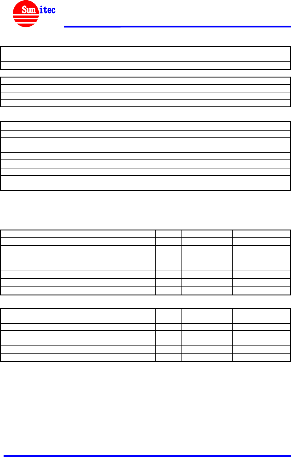
System Architecture
BM153 Class 2 Multimedia Module
CSR, BC57E687C
Jan. 2013
Product Description:
The BM153 is a Class 2 Bluetooth sub-system using BlueCore5-
Multimedia External chipset from leading Bluetooth chipset
supplier Cambridge Silicon Radio.
BM153 interfaces to 8Mbit of external Flash memory When used
with the CSR Bluetooth software stack, it provides a fully compliant
Bluetooth system to V3.0 of the specification for data and voice
communications
The module and device firmware is fully compliant with the
Bluetooth specification V3.0
Applications:
• Hands-free Car Kit
• Stereo Headset
• AV Headphones
• Echo Cancellation
• High Performance Mono Headsets
• Analogue and USB Multimedia Dongles
•
Wireless Speakers
Specifications:
Operating Frequency Band 2.4GHz ~ 2.48GHz unlicensed ISM band
Bluetooth Specification BT V3.0 (V2.1+EDR)
Output Power Class Class 2
Max. Output Power 2.5mW
Date Rate 3Mbps
Channel No. 79
Modulation Type GFSK π/4 DQPSK 8DPSK
Operating Voltage 1.8V / 3.3V
Host Interface USB 1.1 or UART
Audio Interface PCM, I2S, SPDIF
Flash Memory Size 8M,16M, or 32Mbits
Dimension 21mm (L) x 13.5 (W) mm x 2.35mm (H)
Specifications are subject to change without prior notice
Qualified
Product Specification
Spec-BM153-V4.6 Page 2 of 7 www.sunitec-cn.com
®
Electrical Characteristics
Absolute Maximum Rating Min Max
Storage Temperature -40°C +85°C
Supply Voltage, (V_CHG) -0.30V +6.5V
Recommended Operating Conditions Min Max
Operating Temperature Range -20°C +70°C
Supply Voltage, (V_BAT) 2.5V 4.2V
Supply Voltage, (V_CHG) 4.5V 5.75V
Power Consumption Units Average
SCO Connection HV3 (30ms interval sniff mode) mA 21
SCO Connection HV1 mA 40
ACL Data Transfer 115.2Kbps UART no traffic (Master) mA 4.4
ACL Data Transfer 115.2Kbps UART no traffic (Slave) mA 15
CODEC
Microphone inputs and ADC/channel mA TBD
DAC and loudspeaker driver, no signal/channel mA TBD
Digital audio processing subsystem mA TBD
VBAT = 4.2V; f = 2.441GHz; T=20°C
RF Characteristics
Receiver Units Min Typ Max Bluetooth Spec
Sensitivity at 0.1% BER dBm - -90 -86 ≤-70
Maximum Receiver Signal dBm -20 -10 - ≥ -20
C/I Co-Channel dB - 6 11 ≤11
Adjacent Channel Selectivity C/I -1MHz dB - -6 0 ≤0
2nd Adjacent Channel Selectivity C/I -2MHz dB - -38 -30 ≤-30
3rd Adjacent Channel Selectivity C/I -3MHz dB - -45 -40 ≤-40
Image Rejection C/I dB - -16 -9 ≤-9
VBAT = 4.2V; f = 2.4441GHz; T=20°C
Transmitter Units Min Typ Max Bluetooth Spec
RF Output Power dBm 0 3 - -6 to +4
RF Power Control Range dB 16 24 - > 16
RF Power Range Control Resolution dB - 0.5 - -
20dB Bandwidth for Modulated Carrier KHz - 940 1000 <1000
2nd Adjacent Channel Power (+/- 2MHz) dBm - -36 -20 ≤-20
3rd Adjacent Channel Power (+/- 3MHz) dBm - -45 -40 ≤-40
VBAT = 4.2V; f = 2.4441GHz; T=20°C
All specifications including pinouts and electrical specifications may be changed without prior notice
Product Specification
Spec-BM153-V4.6 Page 3 of 7 www.sunitec-cn.com
®
Pin Configurations
PIN NO. NAME TYPE FUNCTION RE-MARK
1 AIO1 Bi-directional Programmable input/output line
2 AIO0 Bi-directional Programmable input/output line
3 RESET CMOS input with
weak internal pull-up
Reset if low. Input debounced so must be low for >5ms to
cause a reset
4 GND GND Ground
5 PIO9 Bi-directional Programmable Input/Output Line
6 PIO10 Bi-directional Programmable Input/Output Line
7 PIO11 Bi-directional Programmable Input/Output Line
8 PIO12 Bi-directional Programmable Input/Output Line
9 PIO13 Bi-directional Programmable Input/Output Line
10 PIO14 Bi-directional Programmable Input/Output Line
11 PIO15 Bi-directional Programmable Input/Output Line
12 GND GND Ground
13 VDD Power +3.3V Supply For 3.3V Version
VDD Power Connect to +1V8 For 1.8V Version
14 VDD_USB Power Positive supply for UART/USB ports, Connect to VDD
15 +1V8 Power +1.8V Supply
16 GND GND Ground
17 USB_DP Bi-directional USB Data Plus
18 USB_DN Bi-directional USB Data Minus
19 UART_RTS CMOS Output UART Request To Send (Active Low)
20 UART_CTS CMOS Input UART Clear To Send (Active Low)
21 UART_RX CMOS Input UART Data Input (Active High)
22 UART_TX CMOS Output UART Data Output (Active High)
23 PCM_IN CMOS Input Synchronous Data Input
24 PCM_SYNC Bi-directional Synchronous Data Sync
25 PCM_CLK Bi-directional Synchronous Data Clock
26 PCM_OUT CMOS Output Synchronous Data Output
27 SPI_CSB CMOS Input Chip Select For Synchronous Serial Interface (Active Low)
28 SPI_MISO CMOS Output Serial Peripheral Interface Data Output
29 SPI_CLK CMOS Input Serial Peripheral Interface Clock
30 SPI_MOSI CMOS Input Serial Peripheral Interface Data Input
31 VRE_IN Analogue Take high to enable switch-mode regulator
32 VDD_BAT Battery terminal +ve Lithium ion/polymer battery positive terminal. Battery
charger output and input to switch-mode regulator
33 GND GND Ground
34 VDD_CHG Charger input Lithium ion/polymer battery charger input
35 LED1 Open drain output LED Driver
36 LED0 Open drain output LED Driver
37 GND GND Ground
38 SPK_L_N Analogue Speaker output negative, left
39 SPK_L_P Analogue Speaker output positive, left
40 SPK_R_N Analogue Speaker output negative, right
41 SPK_R_P Analogue Speaker output positive, right
42 GND_S GND_S Anlogue Signal Ground
43 MIC_BIAS Analogue Microphone bias
44 MIC_B_P Analogue Microphone input positive, right
45 MIC_B_N Analogue Microphone input negative, right
46 MIC_A_P Analogue Microphone input positive, left
47 MIC_A_N Analogue Microphone input negative, left
48 GND GND Ground
49 PIO0 Bi-directional Programmable Input/Output Line
50 PIO1 Bi-directional Programmable Input/Output Line
51 PIO2 Bi-directional Programmable Input/Output Line
52 PIO3 Bi-directional Programmable Input/Output Line
53 PIO4 Bi-directional Programmable Input/Output Line
54 PIO5 Bi-directional Programmable Input/Output Line
55 PIO6 Bi-directional Programmable Input/Output Line
56 PIO7 Bi-directional Programmable Input/Output Line
57 PIO8 Bi-directional Programmable Input/Output Line
58 GND GND Ground
59 RF-IN RF RF Interface
60 GND GND Ground
Product Specification
Spec-BM153-V4.6 Page 4 of 7 www.sunitec-cn.com
®
Recommended Layout patterns:
Product Specification
Spec-BM153-V4.6 Page 5 of 7 www.sunitec-cn.com
®
Recommended Reflow Temperature Profile:
Key features of the profile:
-Initial Ramp=1-2.5℃/sec to 175℃ equilibrium
-Equilibrium time=60 to 80 seconds
-Ramp to Maximum temperature (250℃)=3℃/sec Max
-Time above liquidus temperature(217℃): 45 - 90 seconds
-Device absolute maximum reflow temperature: 250℃
MAC Address:
Each Module has his MAC Address
001D DF XXXXXX
Concerning the dimension of the tab,only printing the last six letters of the LAP on the module.
xxxxxx
5.0 mm
13.0 mm
The tab code pastes style:
Product Specification
Spec-BM153-V4.6 Page 6 of 7 www.sunitec-cn.com
®
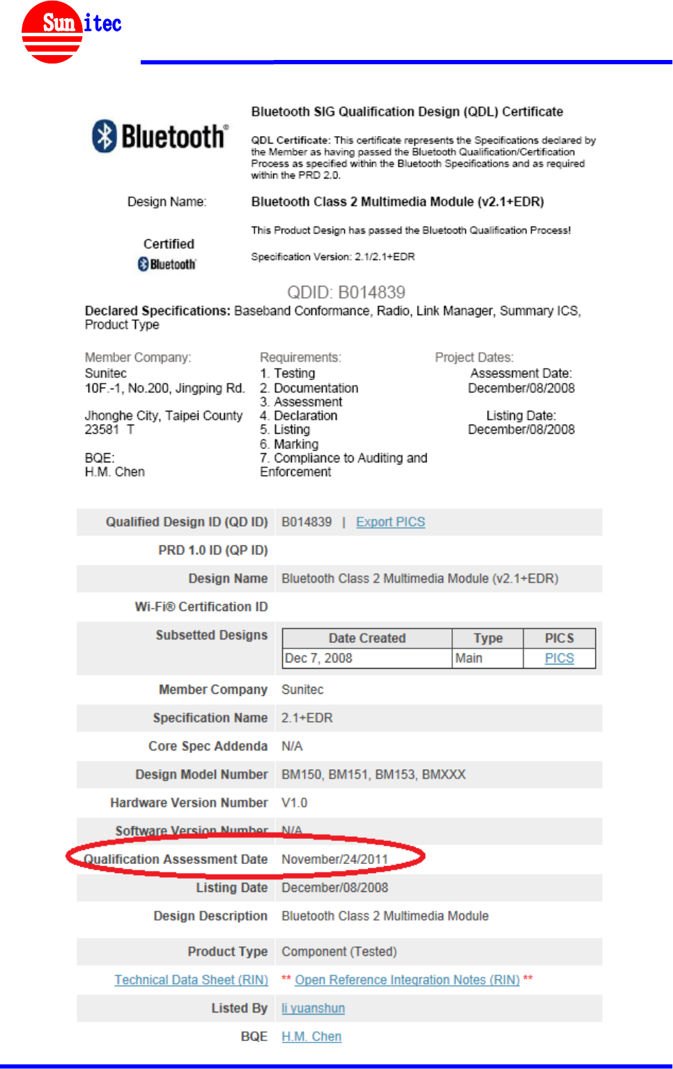
QDL Certificate
Product Specification
Spec-BM153-V4.6 Page 7 of 7 www.sunitec-cn.com
®
Ordering Information
No Items Ordering Code (Class 2) Description
1 BC05mm-ext Module-3V3 BM153 16Mbit Flash Operating Voltage is 3.3V
2 BC05mm-ext Module-3V3 BM153-08 8Mbit Flash Operating Voltage is 3.3V
3 BC05mm-ext Module-3V3 BM153-32 32Mbit Flash Operating Voltage is 3.3V
4 BC05mm-ext Module Test Kit BM153 TK Test kit base BM153
Document References
References Version
Specifications of the Bluetooth System V2.1+EDR, 26 July 2007
BlueCore5-Multimedia External Product Data Sheet CS-121064-DSP2 15 July 2008
Document History
Revision Date History
Draft V0.1 2006-12-12
V1.0 2007-04-12 First release
V2.0 2008-09-11 Update from Revision V1.0
V3.0 2008-09-19 Update from Revision V2.0
V4.0 2009-05-22 Update from V2.0+EDR compliant to V2.1+EDR compliant
V4.1 2009-07-30 Update from printing MAC address “UAP” to “LAP”
V4.2 2009-08-22 Remove BC57E687B-ITB-E4 from BOM
V4.3 2009-12-02 Modify page 3 PIN OUT mistake (Swap AIO0 and AIO1)
V4.4 2011-7-1 Add more order information
V4.5 2011-12-19 Add more order information BM153-32
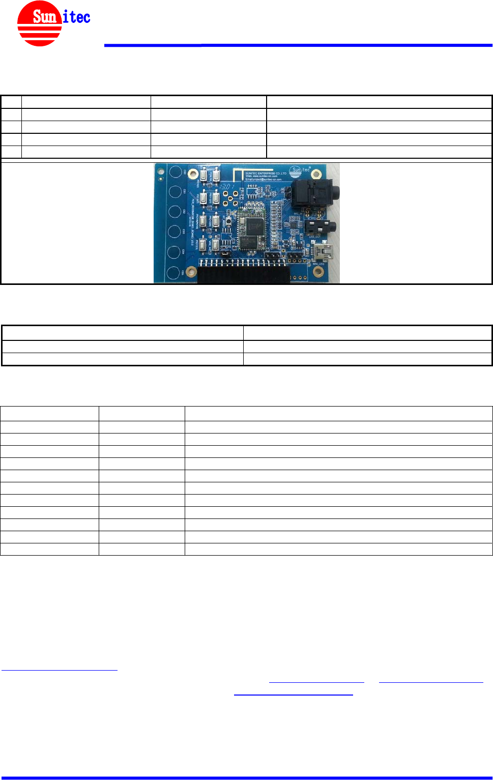
V4.6 2013-01-10 Add BM153 Test board
Contact Information
Sunitec Enterprise Co., Ltd.
Head Office:
3F.,No.98-1,Mincyuan Rd Sindian City, Taipei
County 231,Taiwan
Tel: 886-2-82191696
Fax: 886-2-82191676
http://www.sunitec.com.tw
China Factory:
No.2,Qilin Road 2,Run Tang Ind., Dan-Keng Village Fu
Ming Community, Guan-lan Town, BaoAn District,
Shenzhen GuangDong China
Tel: 86-755-29802983
Fax: 86-755-29802984
E-mail: sales@sunitec-cn.com or project@sunitec-cn.com
Http://www.sunitec-cn.com
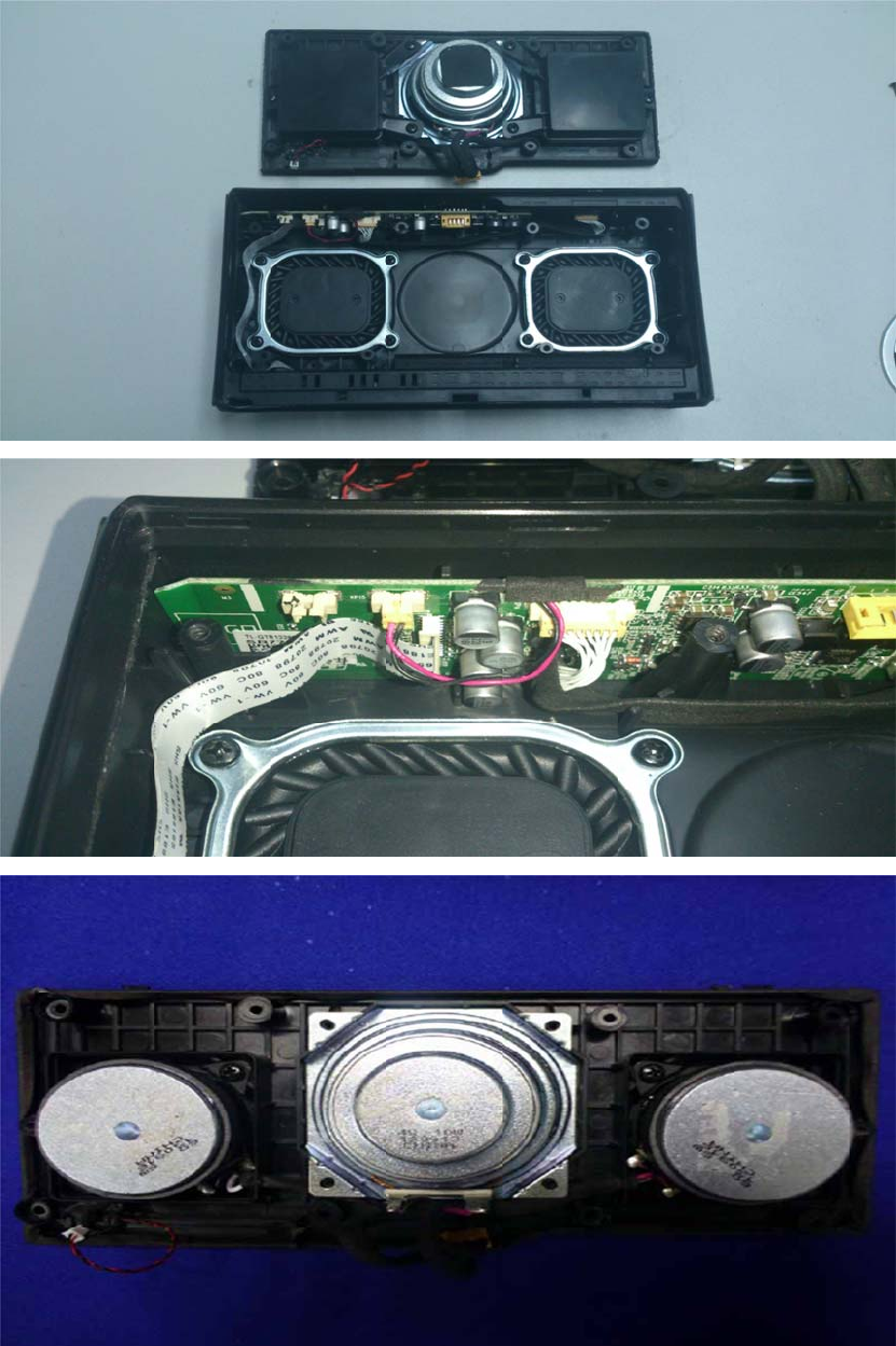
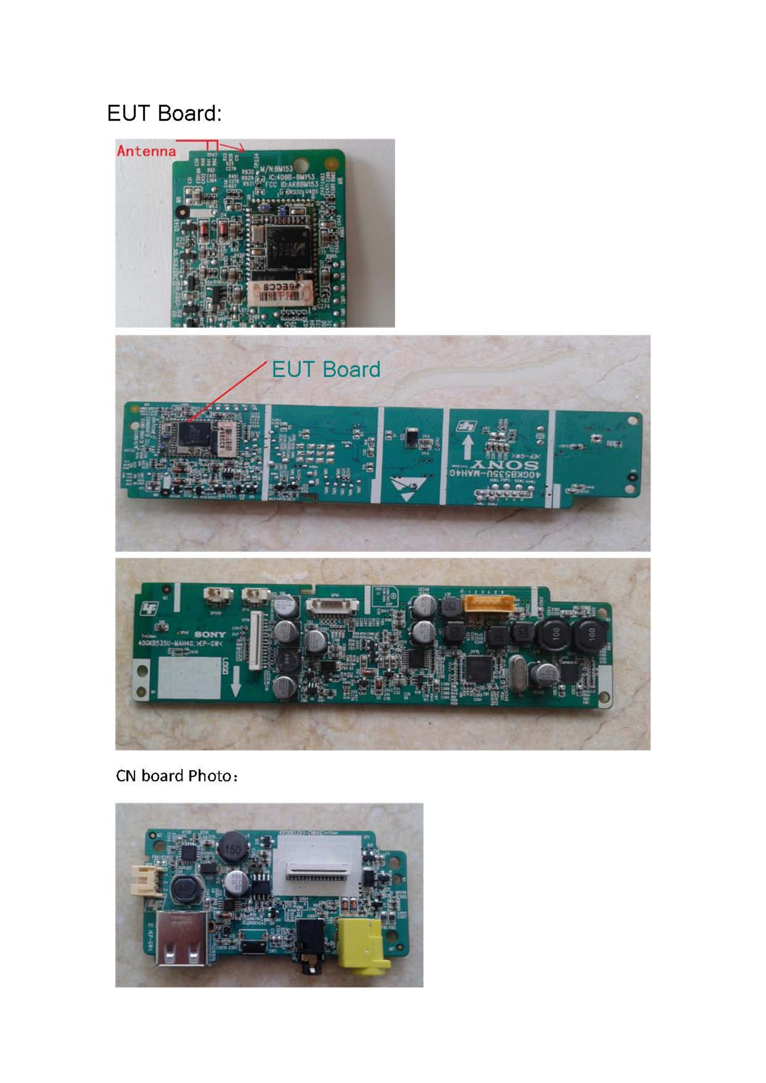
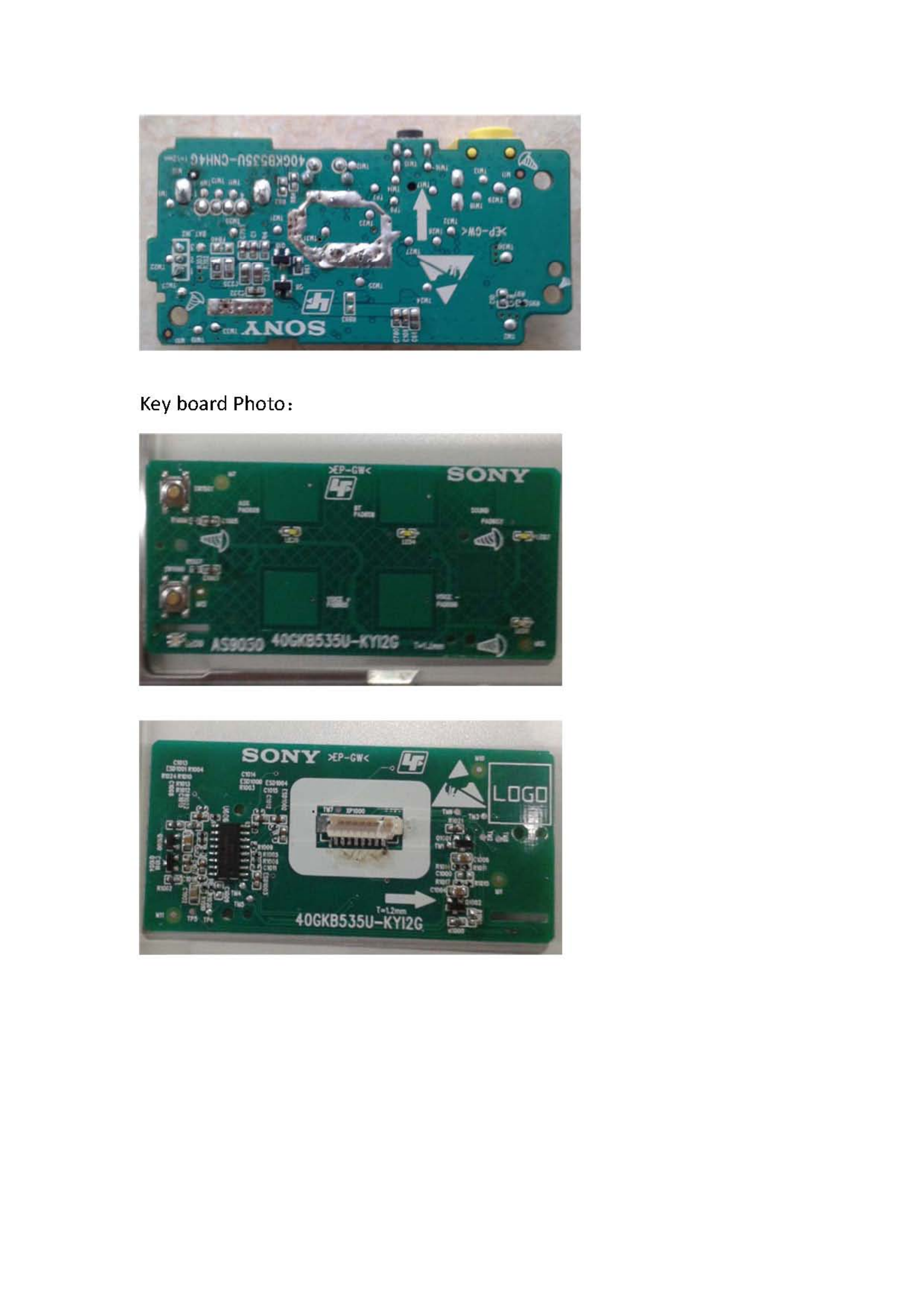
Inte
r
Inte
r
rnalPhoto
rnalPhoto
S
Pers
o
S
Pers
o
S
onyCorpor
a
o
nalAudioS
y
[Model:SR
S
onyCorpor
a
o
nalAudioS
y
[Model:S
R
a
tion
y
stem
S‐X5]
a
tion
y
stem
R
S‐X5
Inte
r
rnalPhoto
S
Pers
o
S
onyCorpor
a
o
nalAudioS
y
[Model:S
R
a
tion
y
stem
R
S‐X5
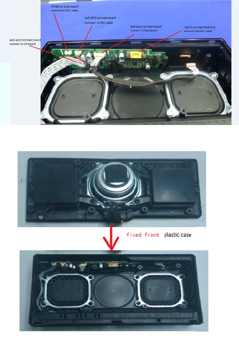
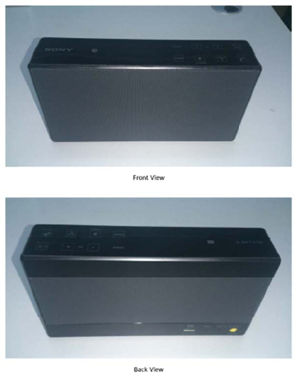
Alli
s
Nex
t
s
ok,fixedth
e
t
:fixedtheir
o
e
speakeran
d
o
nnetandb
d
frontplasti
c
a
ckboard.as
f
c
case.Asfol
f
ollowphoto
l
owphoto
;
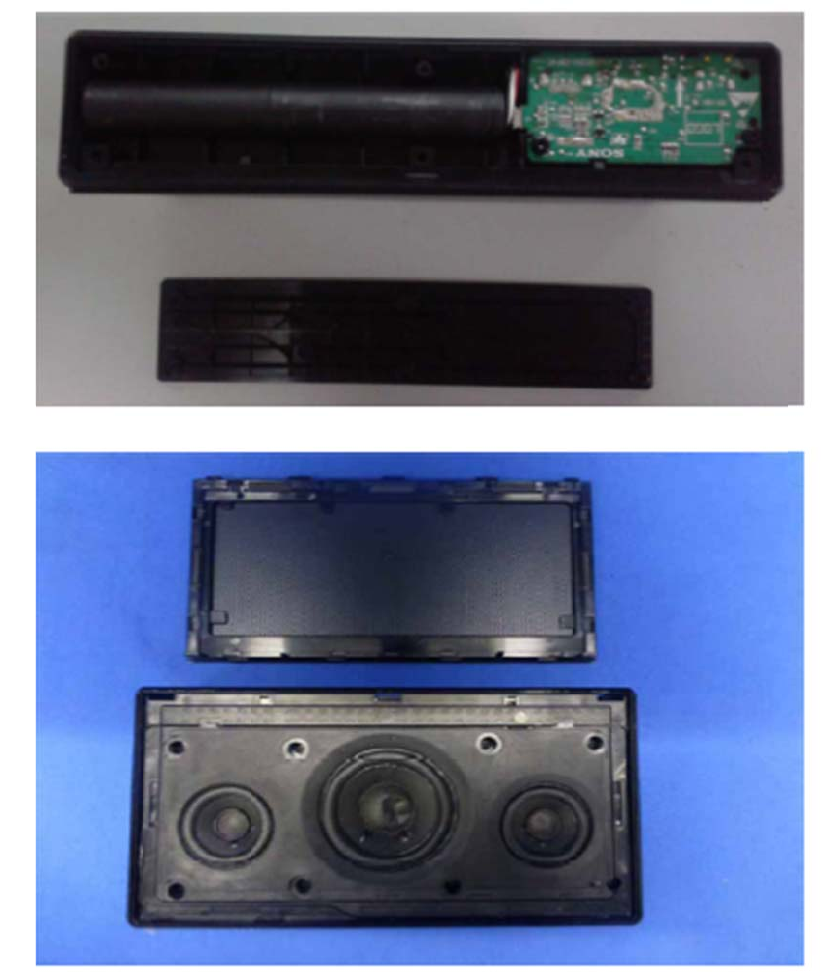
No
w
w
,oneSRS
‐
‐
x5isfixedO
K
K
.asfollow
p
p
hoto.

FCC Statement
Changes or modifications not expressly approved by the party responsible for compliance could
void the user's authority to operate the equipment
This device complies with Part 15 of the FCC Rules. Operation is subject to the following two
conditions: (1) this device may not cause harmful interference, and (2) this device must accept
any interference received, including interference that may cause undesired operation.
IC Statement
This device complies with Industry Canada licence-exempt RSS standard(s). Operation is subject
to the following two conditions: (1) this device may not cause interference, and (2) this device
must accept any interference, including interference that may cause undesired operation of the
device.
Le présent appareil est conforme aux CNR d'Industrie Canada applicables aux appareils radio
exempts de licence. L'exploitation est autorisée aux deux conditions suivantes : (1) l'appareil ne
doit pas produire de brouillage, et (2) l'utilisateur de l'appareil doit accepter tout brouillage
radioélectrique subi, même si le brouillage est susceptible d'en compromettre le fonctionnement.
The end host device should bear the label which indicate "Contains FCC ID:AK8BM153" or
"Contains IC:409B-BM153".