Sony 6220501-BV Transmitter module for mobile applications User Manual 02 0006 Rev A GM47 Design Guidelines
Sony Mobile Communications Inc Transmitter module for mobile applications 02 0006 Rev A GM47 Design Guidelines
Sony >
Contents
- 1. Exhibit 08 Manual
- 2. Exhibit 8 Design Guidelines
- 3. Exhibit 8 Integrators Manual
- 4. revised page
Exhibit 8 Design Guidelines

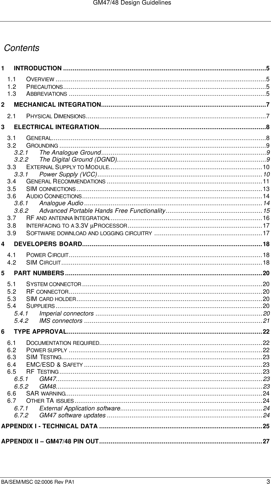
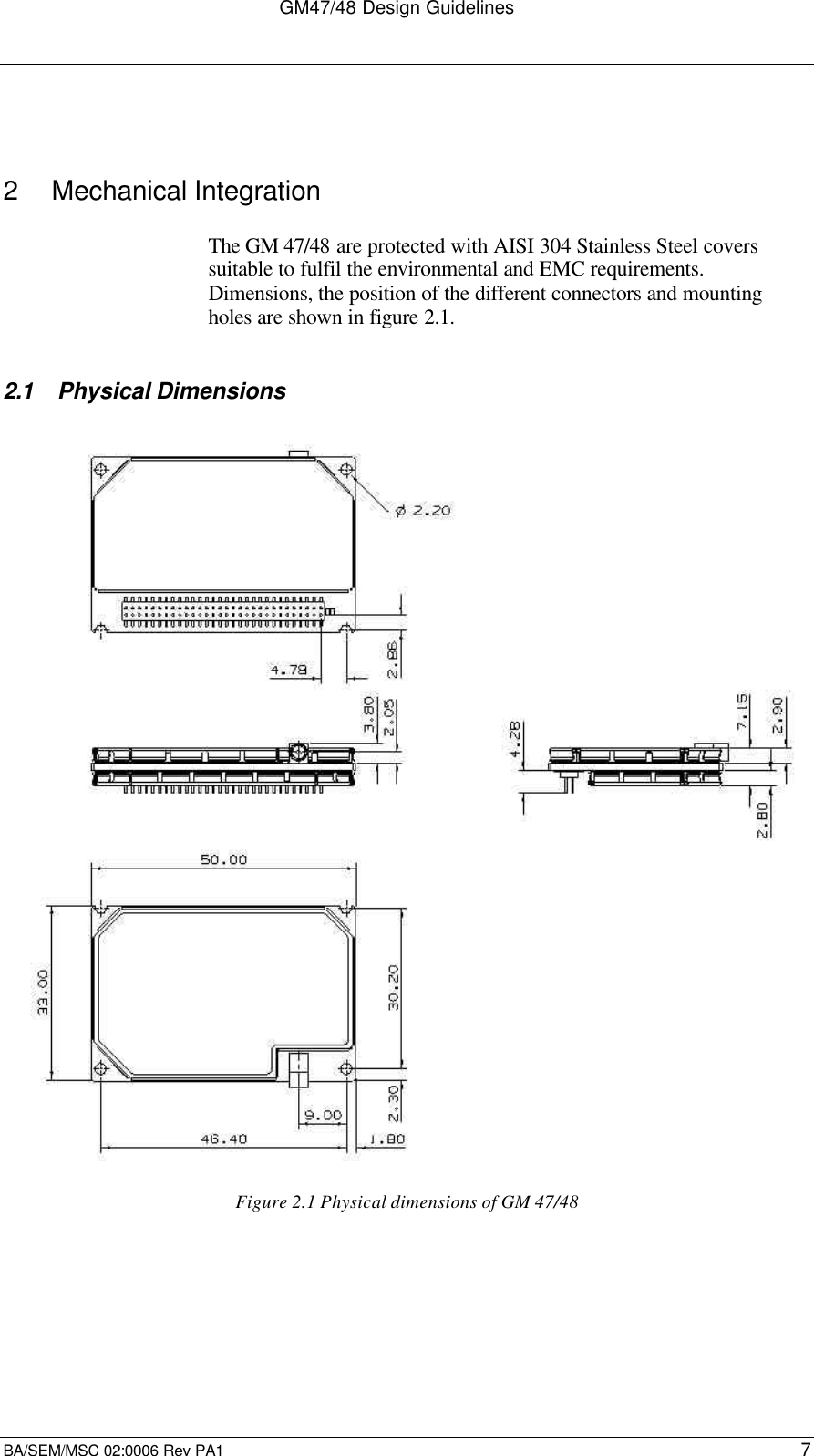
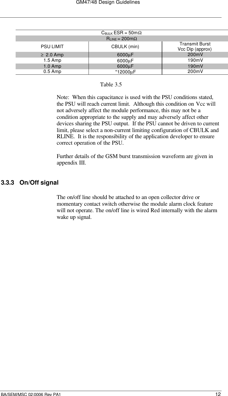
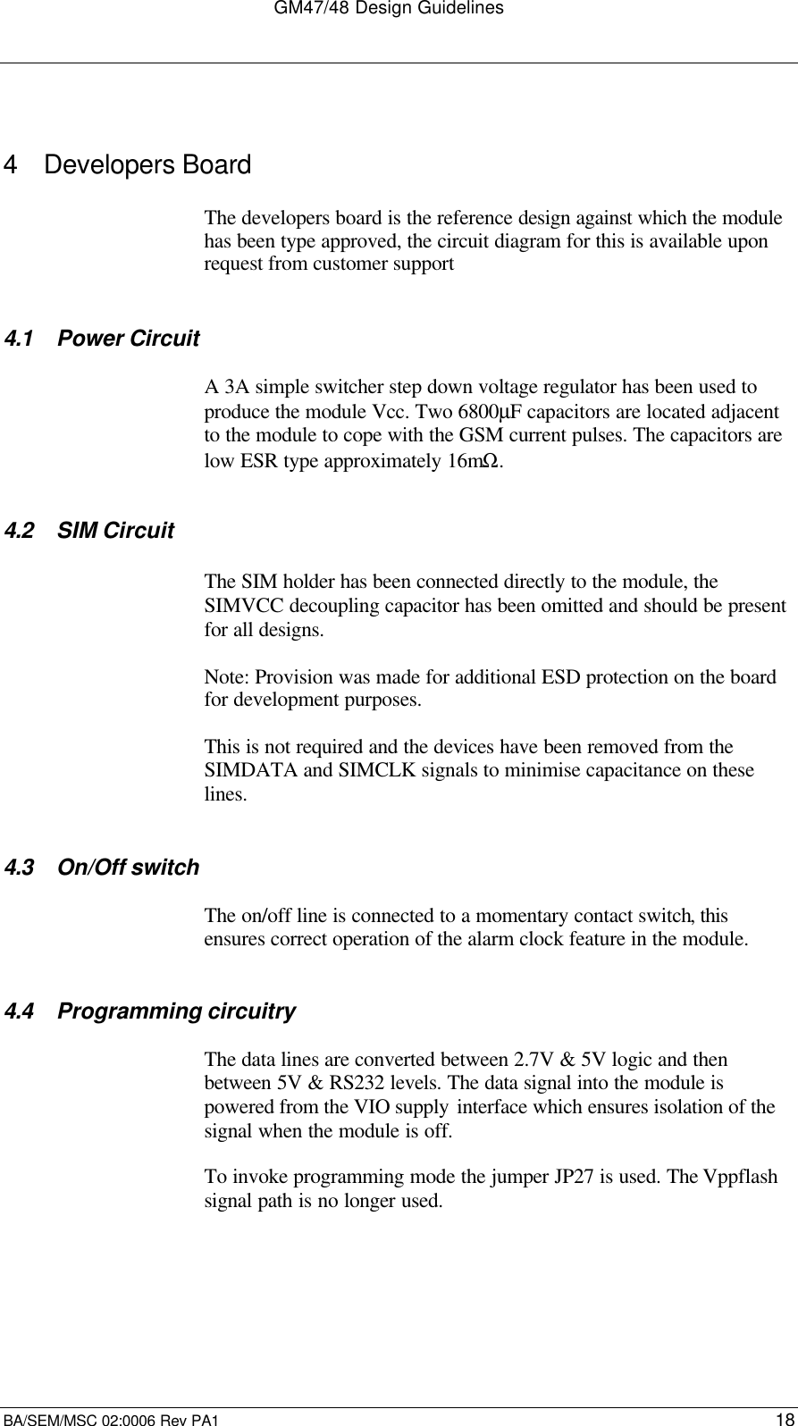
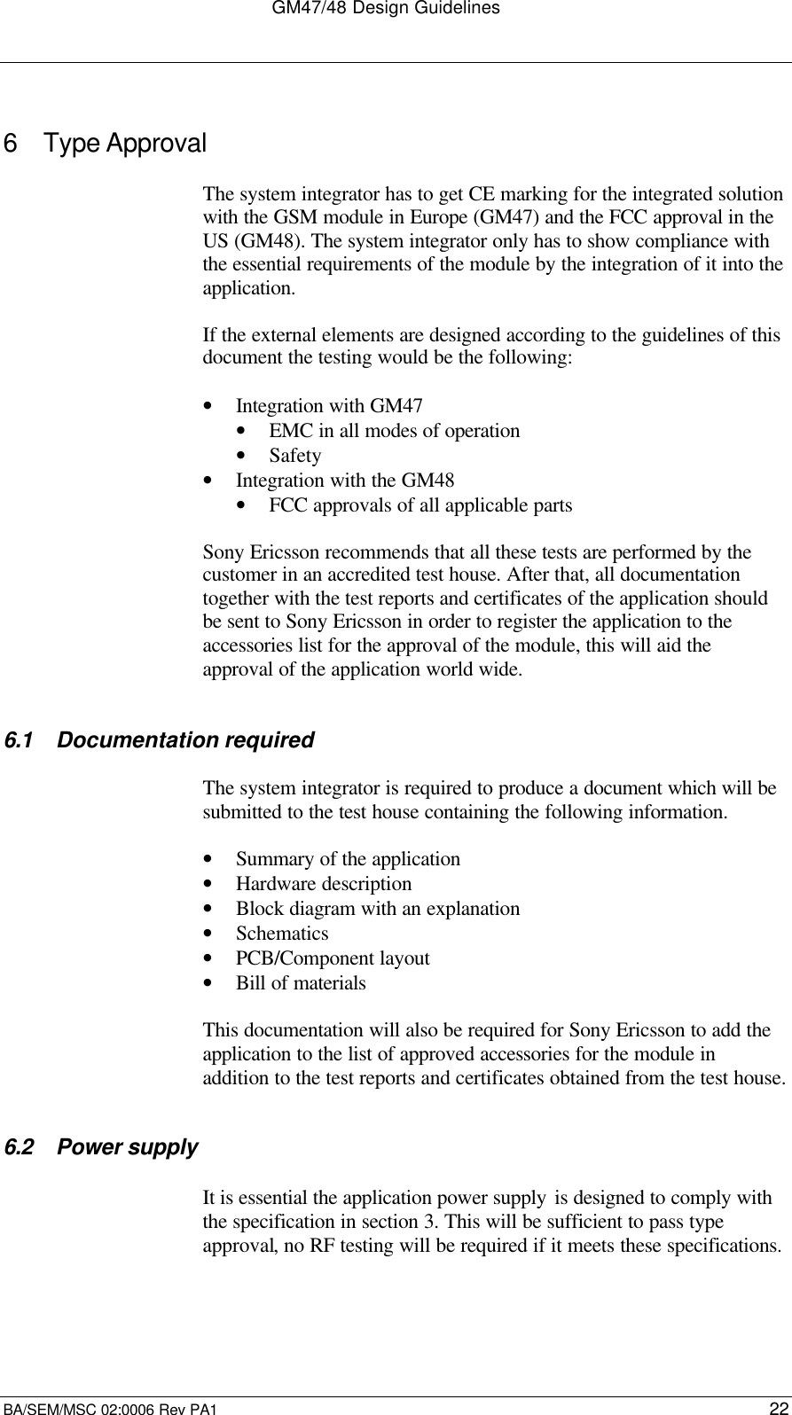
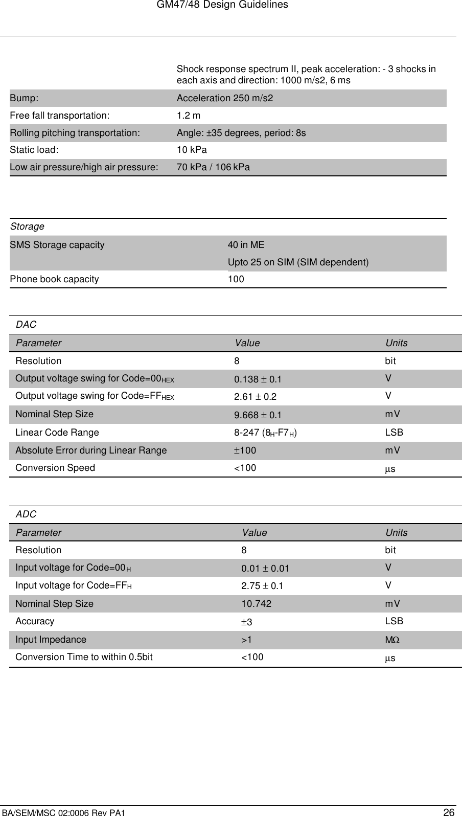
![GM47/48 Design GuidelinesBA/SEM/MSC 02:0006 Rev PA1 113.3.2 General RecommendationsThe power supply conditions for the GM47/48 Vcc connection are asfollows:Maximum voltage drop duringtransmit burst 200mVMaximum Ripple TBD : [estimate 50mV]Table 3.1Recommended ESR on CBULK : <100mΩRecommended Maximum DC resistance between PSU and GM47 Vcc: <200mΩRecommended minimum CBULK : 1000µF [see tables below]The following tables provide a quick indication to recommendedCBULK capacitance to maintain Vcc drop <200mV for different PSUcurrent delivery and DC resistance between PSU and Module Vcc.CBULK ESR = 50mΩRLINE = 50mΩPSU LIMIT CBULK (min) Transmit BurstVcc Dip (approx)≥ 2.0 Amp 1000µF120mV1.5 Amp *2500µF170mV1.0 Amp *6000µF160mV0.5 Amp *10000µF165mVTable 3.2CBULK ESR = 50mΩRLINE = 100mΩPSU LIMIT CBULK (min) Transmit BurstVcc Dip (approx)≥ 2.0 Amp 1500µF200mV1.5 Amp 4000µF150mV1.0 Amp *6000µF170mV0.5 Amp *10000µF180mVTable 3.3CBULK ESR = 50mΩRLINE = 150mΩPSU LIMIT CBULK (min) Transmit BurstVcc Dip (approx)≥ 2.0 Amp 4000µF200mV1.5 Amp 5000µF190mV1.0 Amp *6000µF190mV0.5 Amp *10000µF200mVTable 3.4](https://usermanual.wiki/Sony/6220501-BV.Exhibit-8-Design-Guidelines/User-Guide-247707-Page-11.png)
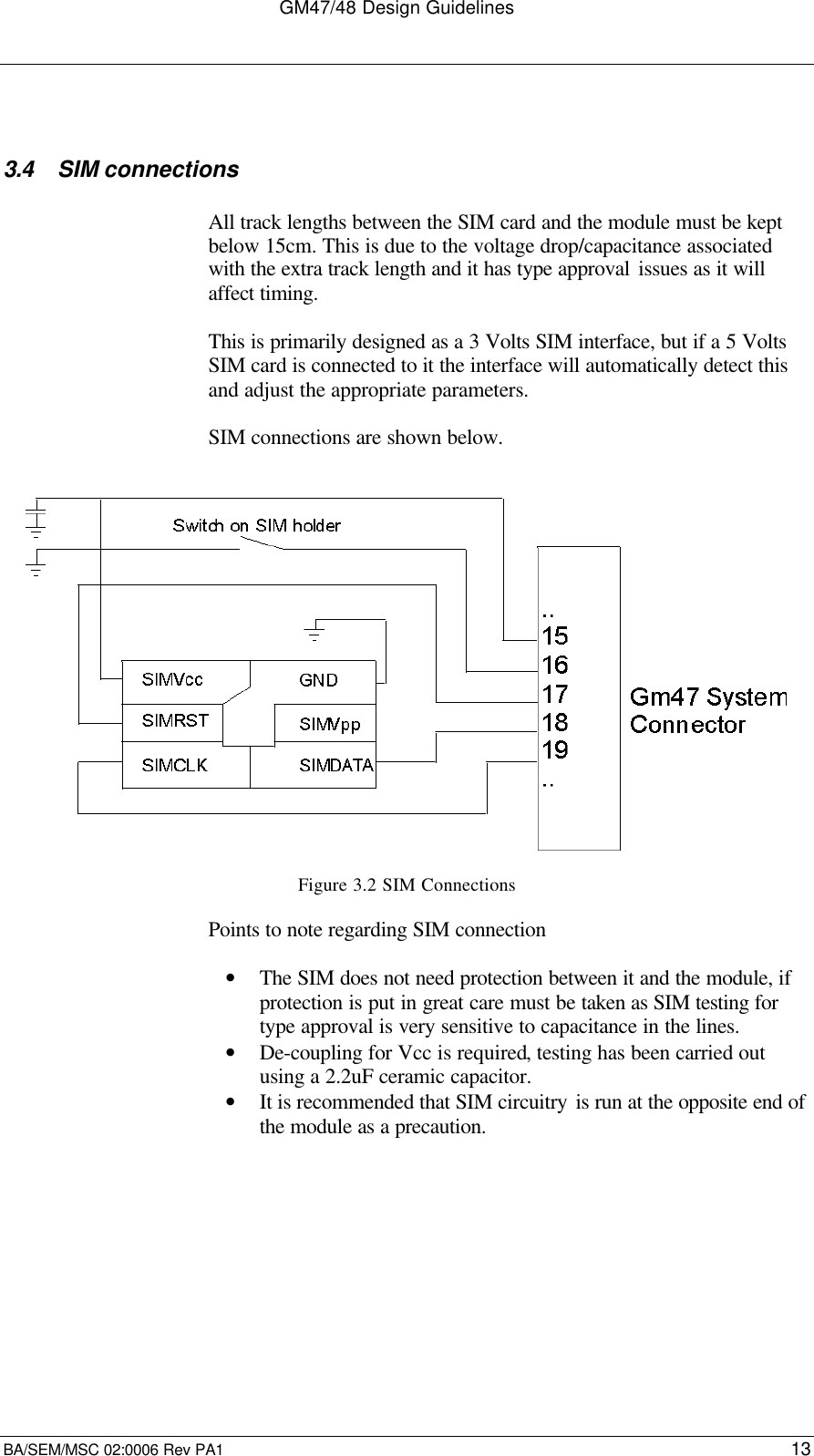
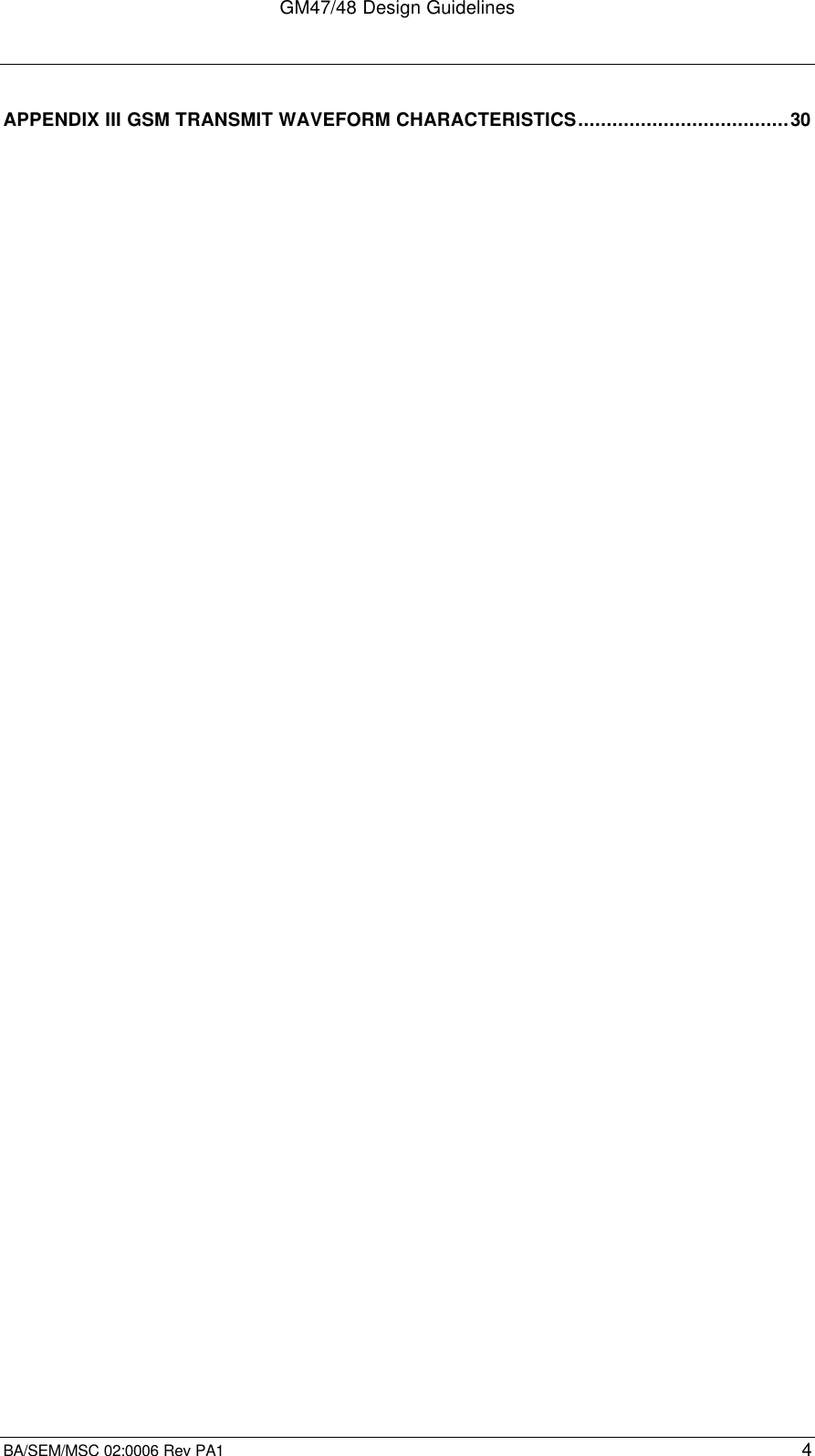
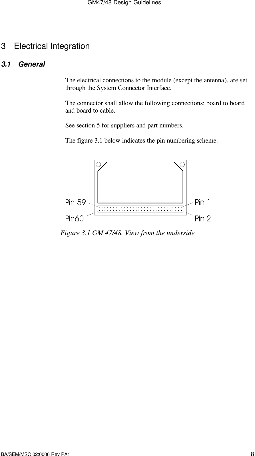
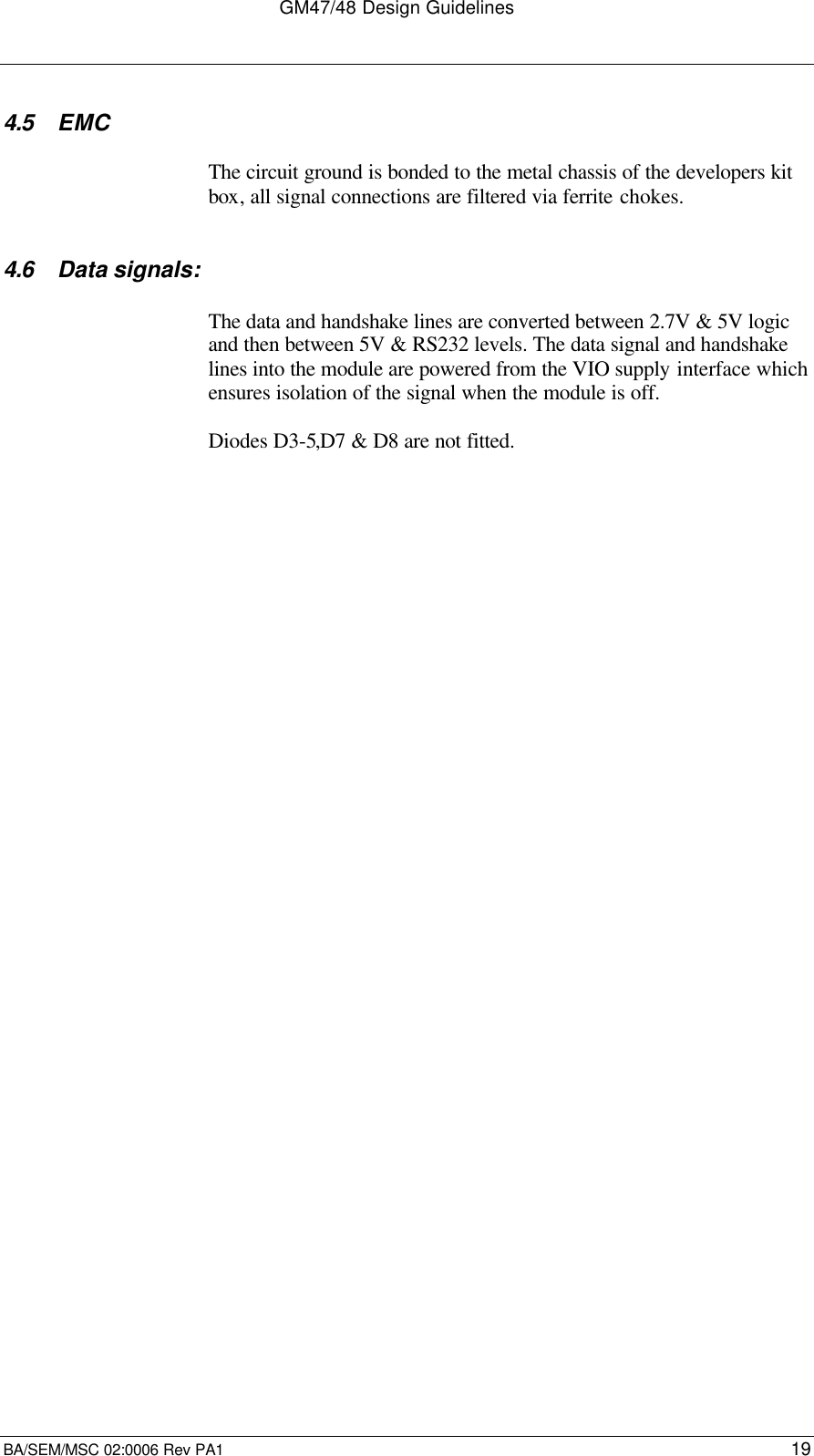
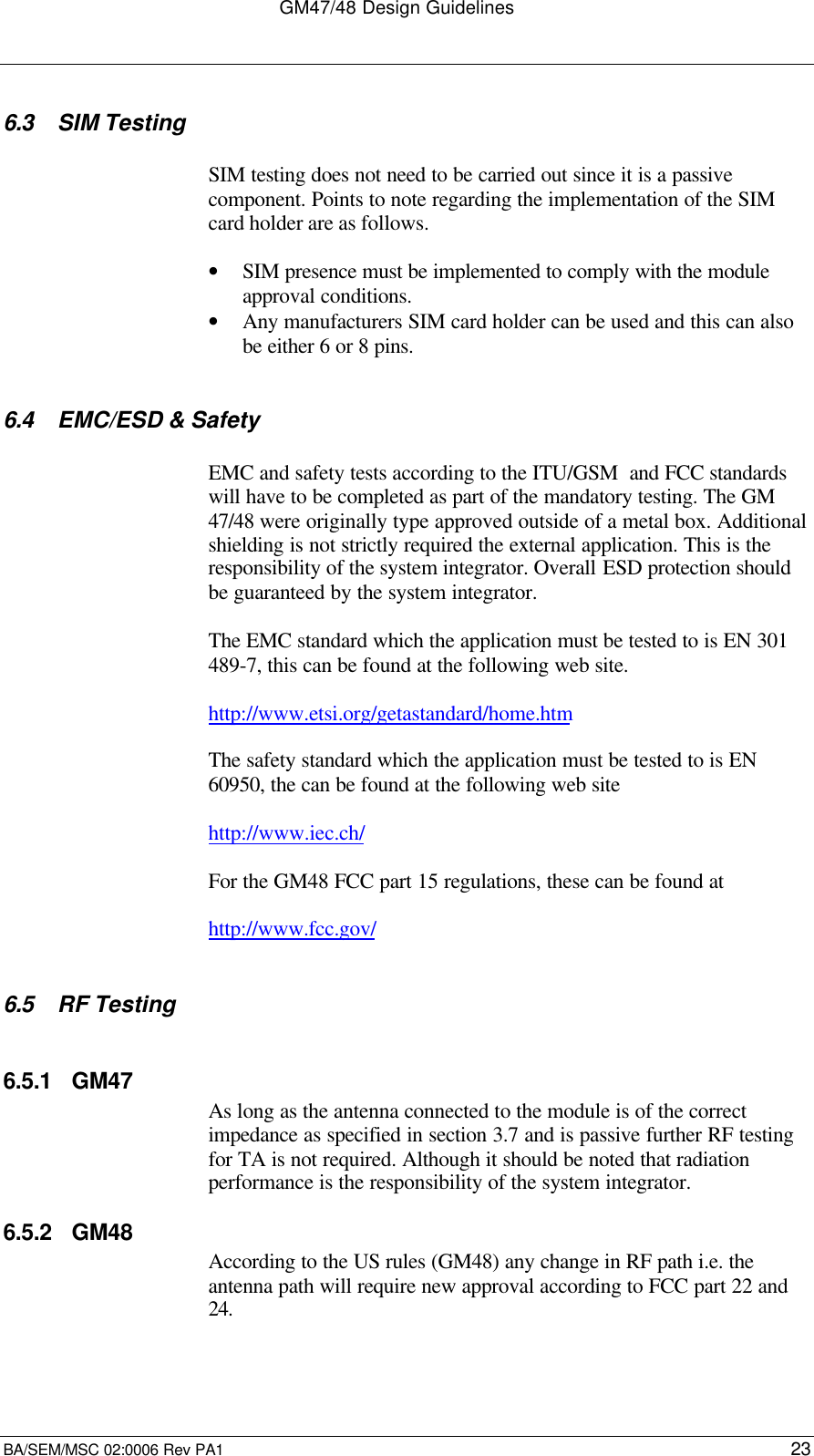
![GM47/48 Design GuidelinesBA/SEM/MSC 02:0006 Rev PA1 15will be used by audio accessories like handsets or Hands Freeequipment.• Portable Hands Free - This state activates a differentamplification factor in the GM47 and activates a microphone biaslevel of 2V in ATMS when a call is in progress.This is the default state at power-on..Audio Circuit Electrical characteristicsAll sources must be AC-coupled except the Portable HandsFreemicrophone, which shall be DC-coupled in order to supply DC currentto the Portable HandsFree microphone. AC coupling prevents incorrectbiasing or damage of the ATMS input. The capacitor must have a valuegreater than shown below to avoid attenuation of low frequencies.Application driving impedance (0.3 – 3.5 kHz) ≤ 300 ΩAC coupling capacitance ≥ 1 µFModule input impedance (0.3 – 3.5 kHz) > 50 kΩLow frequency cut-off. (-3 dB) 300 Hz ± 50 HzHigh frequency cut-off. (-3 dB) > 3500 ± 50 HzHands-Freemode 0VOutput DC bias level PortableHands FreeMode2.0V ± 0.1VAdditional Gain in Portable Hands Free Mode 28.5 dBTable 1. ATMS Levels. Audio Levels3.5.2 Advanced Portable Hands Free FunctionalityThis functionality consists in the detection of a push button pressconnecting ATMS to AGND for a certain period of time. This willcreate a change in the microphone DC bias level.Microphone bias current at 2V1< 0.3 mAActivated2< 100 ΩDC impedance for push button Deactivated3> 10 kΩ [TBC]Portable Handsfree electrical data 1 Bias current >0.7mA will cause false indication of button activation (Threshold is 100mV).2 2V x ( 100 Ω / ( 2700 Ω + 100 Ω )) = 71 mV. Threshold is 100mV.3 Lower impedance will reduce bias on microphone.](https://usermanual.wiki/Sony/6220501-BV.Exhibit-8-Design-Guidelines/User-Guide-247707-Page-15.png)
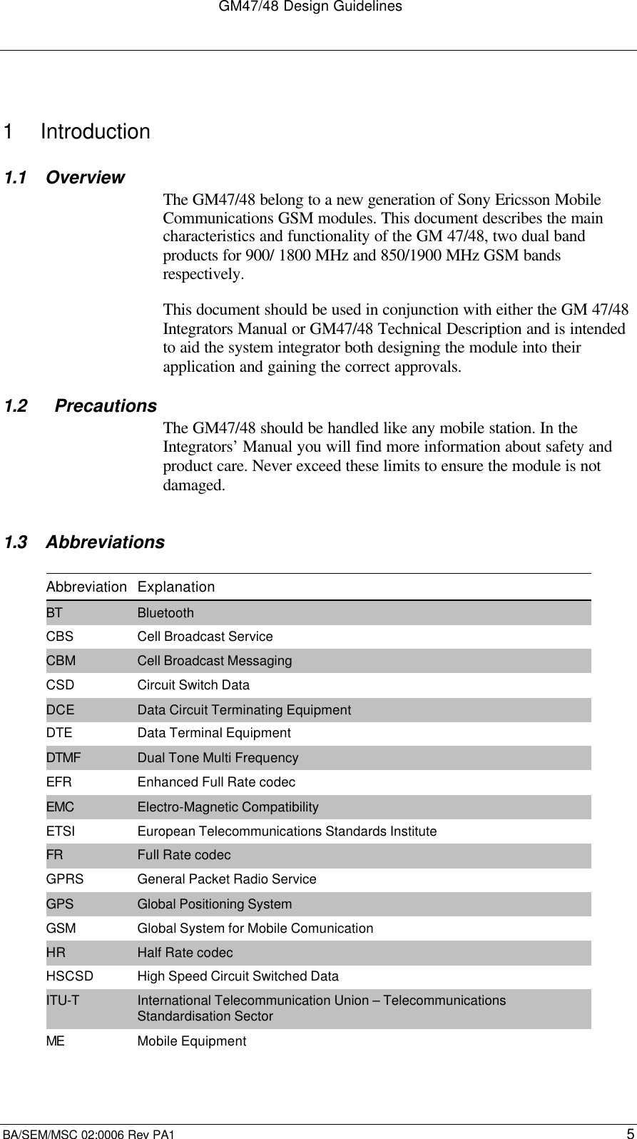
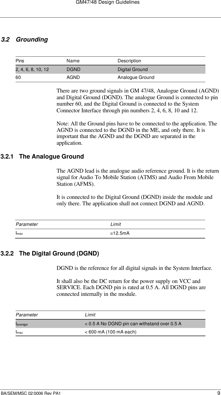
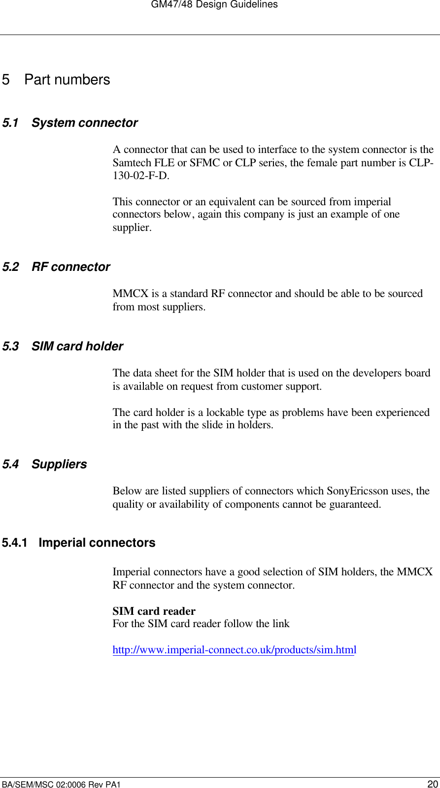
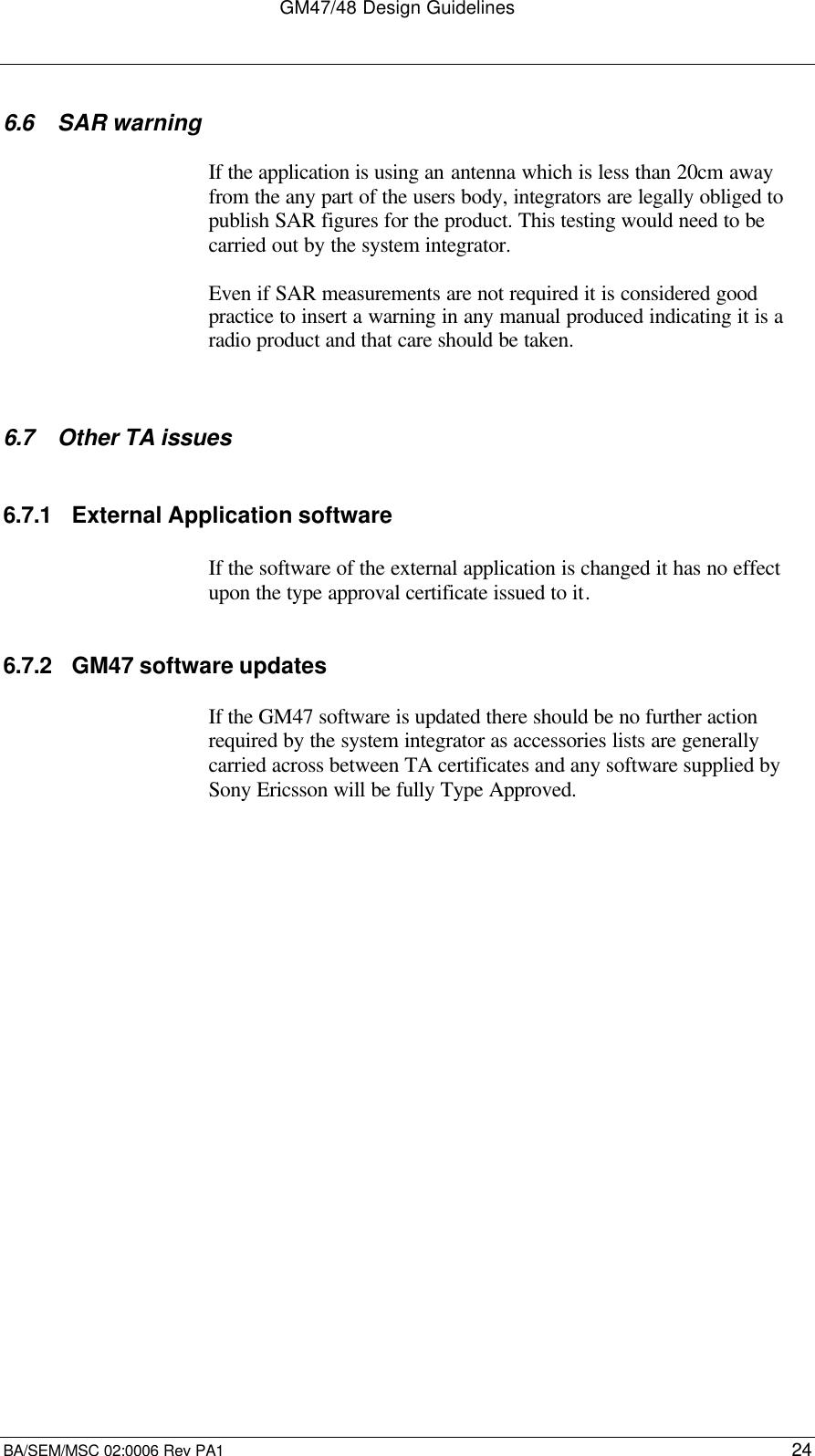
![GM47/48 Design GuidelinesBA/SEM/MSC 02:0006 Rev PA1 16AFMS is the analogue audio output from the module. When it is active,the output is derived from the PCM digital audio by the decoder part ofthe CODEC. The PCM data comes from PCMI on the systemconnector.It is also used as an ear-piece driver for the Portable Hands Freeaccessory.Zout4 (0.3 – 3.5 kHz) ≅ 120 ΩOutput capacitance 2.2 µFDrive capability into 5 kΩ (0.3 – 3.5 kHz) > 2.4 Vpp [TBC]Drive capability into1.5 kΩ (0.3 – 3.5 kHz) > 2.2 Vpp [TBC]Levels5(THD<5%)Drive capability into 150 Ω (at 1 kHz) > 1.3 Vpp [TBC]Table 2. AFMS Levels. Audio Levels3.6 RF and antenna IntegrationThe rules for RF and antenna integration are general good practiceguidelines i.e.• Ensure the antenna is a good 50Ω match across the GSM 900/1800bands for GM47 and GSM 850/1900 bands for GM48.• Antenna installation should be, where possible, not close to largemetal objects as this will affect the matching mentioned above.• A specifically designed antenna for the GSM signals beingoperated at will ensure the best reception.If these are followed there should be no issues in terms of RF.Please also see section 6.6 regarding SAR. 4 Output impedance includes impedance of EMC filter which is 100 Ω.5 Need to check output drive levels with 100R EMI filter.](https://usermanual.wiki/Sony/6220501-BV.Exhibit-8-Design-Guidelines/User-Guide-247707-Page-16.png)
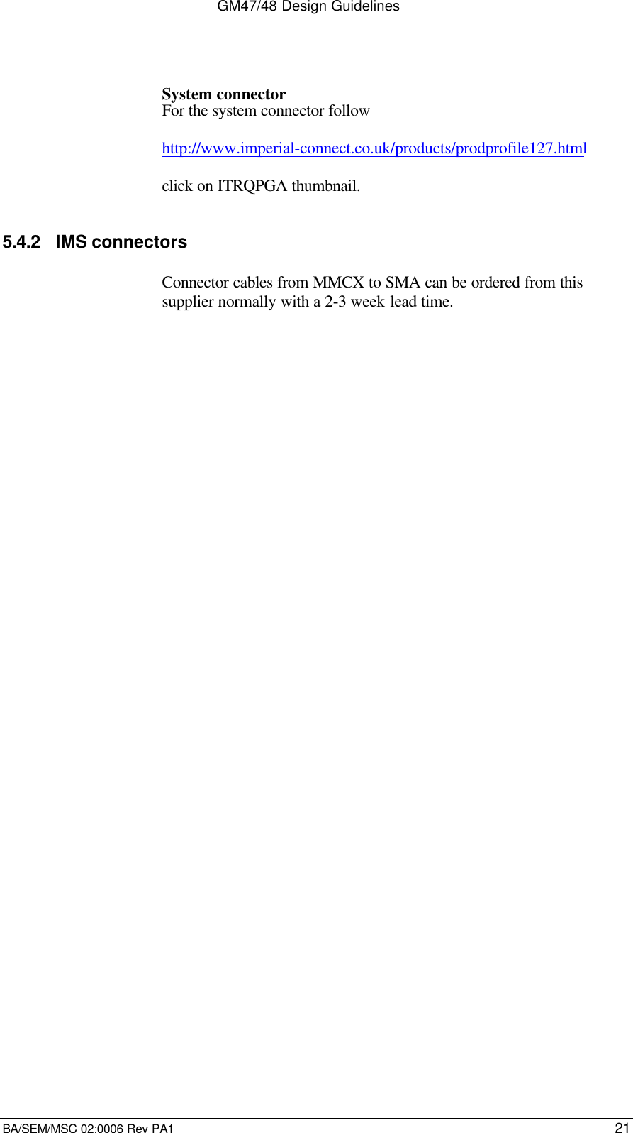
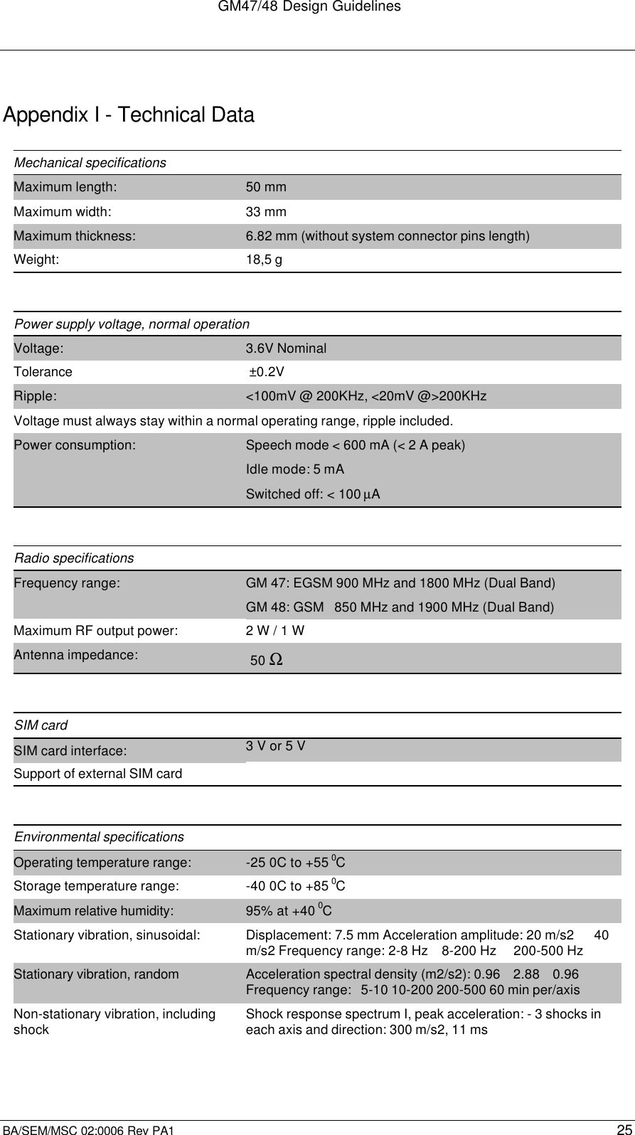
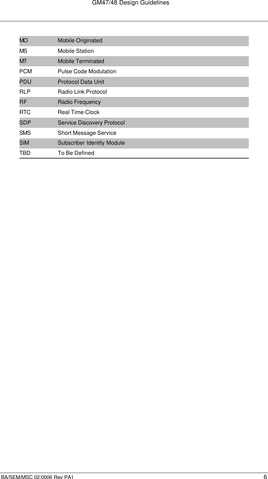
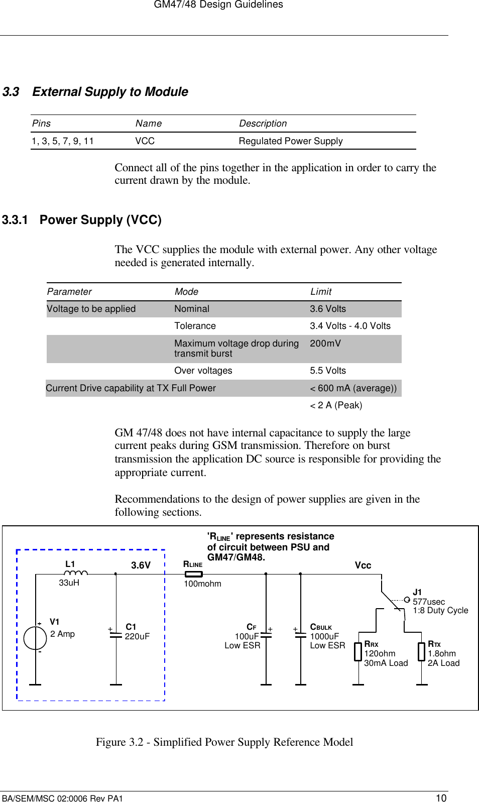
![GM47/48 Design GuidelinesBA/SEM/MSC 02:0006 Rev PA1 2832. TIMESTAMP ODig. 2.75 TimestampTimestamp is reserved for future use, if A-GPS is implemented on network side.33. LED ODig. 2.75 Flashing LED34. VIO OPower Out 2.75 Module powered indication.The VIO is a 2.75 V output that couldpower external devices to transmit datatowards the GSM device to a 75mA max.35. TX_ON ODig 2.75 This output shall indicate when the GSMmodule is going to transmit the burst.36. RI ODig. 2.75 Ring Indicator37. DTR IDig. 2.75 Data Terminal Ready38. DCD ODig. 2.75 Data Carrier Detect39. RTS IDig. 2.75 Request To Send40. CTS ODig. 2.75 Clear To Send41. TD IDig. 2.75 Transmitted DataData from DTE (host) to DCE (module).[former DTMS]42. RD ODig. 2.75 Received DataData from DCE (module) to DTE (host).[former DFMS]43. TD3 IDig. 2.75 UART3 TransmissionData from DTE (host) to DCE (module).[former DTMS]44. RD3 ODig. 2.75 UART3 ReceptionData from DTE (host) to DCE (module).[former DTMS]Data from DCE (module) to DTE (host).[former DFMS]45. TD2 IDig. 2.75 UART2 ReceptionFormer CTMS. Used for flashing46. RD2 ODig. 2.75 UART2 TransmissionData from DCE (module) to DTE (host).[former DFMS]Former CFMS. Used for flashing47. PCMULD IDig. 2.75 DSP PCM digital audio input48. PCMDLD ODig. 2.75 DSP PCM digital audio output49. PCMO ODig. 2.75 Codec PCM digital audio output50. PCMI IDig. 2.75 Codec PCM digital audio input51. PCMSYNC ODig. 2.75 DSP PCM frame sync52. PCMCLK ODig. 2.75 DSP PCM clock output53. MICP IAnalogue Microphone input positive54. MICN IAnalogue Microphone input negative55. BEARP OAnalogue Speaker output positive](https://usermanual.wiki/Sony/6220501-BV.Exhibit-8-Design-Guidelines/User-Guide-247707-Page-28.png)