Sony 6220501-BV Transmitter module for mobile applications User Manual 02 0006 Rev A GM47 Design Guidelines
Sony Mobile Communications Inc Transmitter module for mobile applications 02 0006 Rev A GM47 Design Guidelines
Sony >
Contents
- 1. Exhibit 08 Manual
- 2. Exhibit 8 Design Guidelines
- 3. Exhibit 8 Integrators Manual
- 4. revised page
Exhibit 8 Design Guidelines

GM 47/GM 48
Design Guidelines

CE
The product described in this manual conforms to the TTE directive 91/263/EEC and EMC directive
89/336/EEC. The product fulfils the requirements according to ETS 300 342-1.
The information contained in this document is the proprietary information of Sony Ericsson Mobile
Communications. The contents are confidential and any disclosure to persons other than the officers,
employees, agents or subcontractors of the owner or licensee of this document, without the prior written
consent of Sony Ericsson Mobile Communications, is strictly prohibited.
Further, no portion of this publication may be reproduced, stored in a retrieval system, or transmitted in
any form or by any means, electronic or mechanical, including photocopying and recording, without the
prior written consent of Sony Ericsson Mobile Communications, the copyright holder.
First edition (January 2002)
Sony Ericsson Mobile Communications. publishes this manual without making any warranty as to the
content contained herein. Further Sony Ericsson Mobile Communications. reserves the right to make
modifications, additions and deletions to this manual due to typographical errors, inaccurate information,
or improvements to programs and/or equipment at any time and without notice. Such changes will,
nevertheless be incorporated into new editions of this manual.
All rights reserved.
©Sony Ericsson Mobile Communications., 2002
Publication number:
Printed in UK
Trademarks
AIX is a trademark owned by International Business Machines Corporation

GM47/48 Design Guidelines
BA/SEM/MSC 02:0006 Rev PA1 3
Contents
1INTRODUCTION ...........................................................................................................5
1.1 OVERVIEW ...............................................................................................................5
1.2 PRECAUTIONS...........................................................................................................5
1.3 ABBREVIATIONS ........................................................................................................5
2MECHANICAL INTEGRATION.......................................................................................7
2.1 PHYSICAL DIMENSIONS...............................................................................................7
3ELECTRICAL INTEGRATION........................................................................................8
3.1 GENERAL.................................................................................................................8
3.2 GROUNDING .............................................................................................................9
3.2.1 The Analogue Ground.......................................................................................9
3.2.2 The Digital Ground (DGND)...............................................................................9
3.3 EXTERNAL SUPPLY TO MODULE.................................................................................10
3.3.1 Power Supply (VCC).......................................................................................10
3.4 GENERAL RECOMMENDATIONS ..................................................................................11
3.5 SIM CONNECTIONS ..................................................................................................13
3.6 AUDIO CONNECTIONS...............................................................................................14
3.6.1 Analogue Audio..............................................................................................14
3.6.2 Advanced Portable Hands Free Functionality...................................................15
3.7 RF AND ANTENNA INTEGRATION.................................................................................16
3.8 INTERFACING TO A 3.3V µPROCESSOR.......................................................................17
3.9 SOFTWARE DOWNLOAD AND LOGGING CIRCUITRY .........................................................17
4DEVELOPERS BOARD...............................................................................................18
4.1 POWER CIRCUIT......................................................................................................18
4.2 SIM CIRCUIT..........................................................................................................18
5PART NUMBERS........................................................................................................20
5.1 SYSTEM CONNECTOR ...............................................................................................20
5.2 RF CONNECTOR......................................................................................................20
5.3 SIM CARD HOLDER..................................................................................................20
5.4 SUPPLIERS .............................................................................................................20
5.4.1 Imperial connectors ........................................................................................20
5.4.2 IMS connectors ..............................................................................................21
6TYPE APPROVAL.......................................................................................................22
6.1 DOCUMENTATION REQUIRED......................................................................................22
6.2 POWER SUPPLY ......................................................................................................22
6.3 SIM TESTING..........................................................................................................23
6.4 EMC/ESD & SAFETY ..............................................................................................23
6.5 RF TESTING ...........................................................................................................23
6.5.1 GM47.............................................................................................................23
6.5.2 GM48.............................................................................................................23
6.6 SAR WARNING........................................................................................................24
6.7 OTHER TA ISSUES ...................................................................................................24
6.7.1 External Application software...........................................................................24
6.7.2 GM47 software updates ..................................................................................24
APPENDIX I - TECHNICAL DATA ......................................................................................25
APPENDIX II – GM47/48 PIN OUT......................................................................................27

GM47/48 Design Guidelines
BA/SEM/MSC 02:0006 Rev PA1 4
APPENDIX III GSM TRANSMIT WAVEFORM CHARACTERISTICS.....................................30

GM47/48 Design Guidelines
BA/SEM/MSC 02:0006 Rev PA1 5
1 Introduction
1.1 Overview
The GM47/48 belong to a new generation of Sony Ericsson Mobile
Communications GSM modules. This document describes the main
characteristics and functionality of the GM 47/48, two dual band
products for 900/ 1800 MHz and 850/1900 MHz GSM bands
respectively.
This document should be used in conjunction with either the GM 47/48
Integrators Manual or GM47/48 Technical Description and is intended
to aid the system integrator both designing the module into their
application and gaining the correct approvals.
1.2 Precautions
The GM47/48 should be handled like any mobile station. In the
Integrators’ Manual you will find more information about safety and
product care. Never exceed these limits to ensure the module is not
damaged.
1.3 Abbreviations
Abbreviation Explanation
BT Bluetooth
CBS Cell Broadcast Service
CBM Cell Broadcast Messaging
CSD Circuit Switch Data
DCE Data Circuit Terminating Equipment
DTE Data Terminal Equipment
DTMF Dual Tone Multi Frequency
EFR Enhanced Full Rate codec
EMC Electro-Magnetic Compatibility
ETSI European Telecommunications Standards Institute
FR Full Rate codec
GPRS General Packet Radio Service
GPS Global Positioning System
GSM Global System for Mobile Comunication
HR Half Rate codec
HSCSD High Speed Circuit Switched Data
ITU-T International Telecommunication Union – Telecommunications
Standardisation Sector
ME Mobile Equipment

GM47/48 Design Guidelines
BA/SEM/MSC 02:0006 Rev PA1 6
MO Mobile Originated
MS Mobile Station
MT Mobile Terminated
PCM Pulse Code Modulation
PDU Protocol Data Unit
RLP Radio Link Protocol
RF Radio Frequency
RTC Real Time Clock
SDP Service Discovery Protocol
SMS Short Message Service
SIM Subscriber Identity Module
TBD To Be Defined
GM47/48 Design Guidelines
BA/SEM/MSC 02:0006 Rev PA1 7
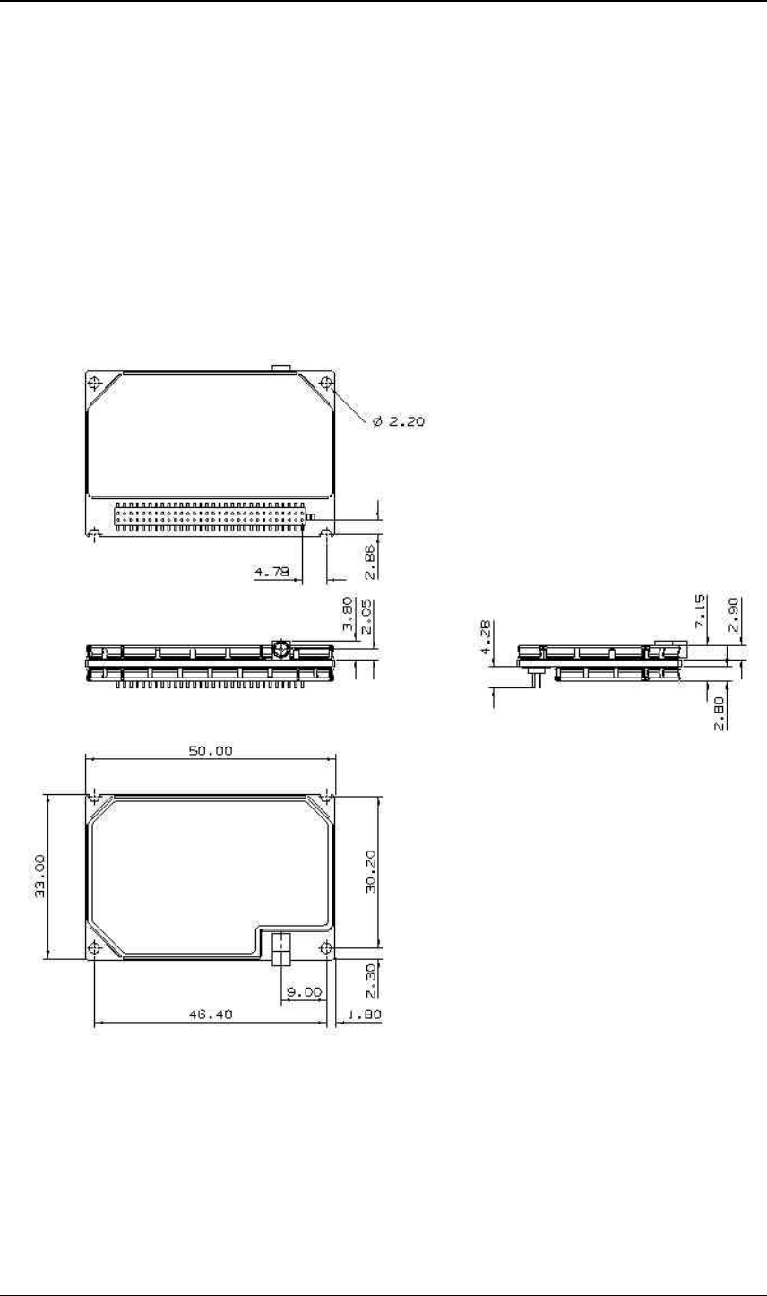
2 Mechanical Integration
The GM 47/48 are protected with AISI 304 Stainless Steel covers
suitable to fulfil the environmental and EMC requirements.
Dimensions, the position of the different connectors and mounting
holes are shown in figure 2.1.
2.1 Physical Dimensions
Figure 2.1 Physical dimensions of GM 47/48
GM47/48 Design Guidelines
BA/SEM/MSC 02:0006 Rev PA1 8
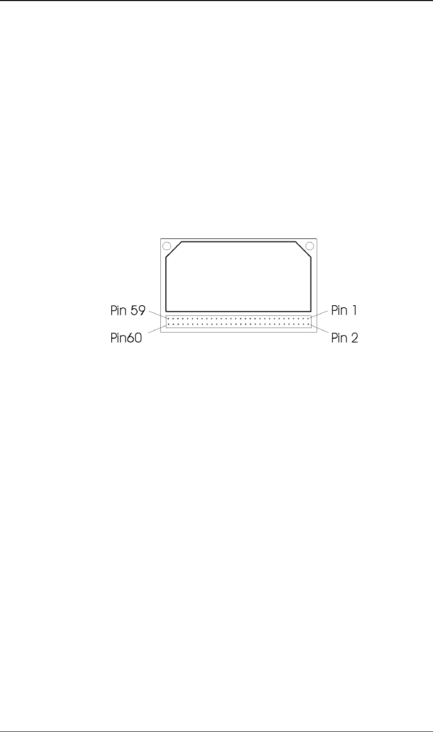
3 Electrical Integration
3.1 General
The electrical connections to the module (except the antenna), are set
through the System Connector Interface.
The connector shall allow the following connections: board to board
and board to cable.
See section 5 for suppliers and part numbers.
The figure 3.1 below indicates the pin numbering scheme.
Figure 3.1 GM 47/48. View from the underside

GM47/48 Design Guidelines
BA/SEM/MSC 02:0006 Rev PA1 9
3.2 Grounding
Pins Name Description
2, 4, 6, 8, 10, 12 DGND Digital Ground
60 AGND Analogue Ground
There are two ground signals in GM 47/48, Analogue Ground (AGND)
and Digital Ground (DGND). The analogue Ground is connected to pin
number 60, and the Digital Ground is connected to the System
Connector Interface through pin numbers 2, 4, 6, 8, 10 and 12.
Note: All the Ground pins have to be connected to the application. The
AGND is connected to the DGND in the ME, and only there. It is
important that the AGND and the DGND are separated in the
application.
3.2.1 The Analogue Ground
The AGND lead is the analogue audio reference ground. It is the return
signal for Audio To Mobile Station (ATMS) and Audio From Mobile
Station (AFMS).
It is connected to the Digital Ground (DGND) inside the module and
only there. The application shall not connect DGND and AGND.
Parameter Limit
Imax ≅12.5mA
3.2.2 The Digital Ground (DGND)
DGND is the reference for all digital signals in the System Interface.
It shall also be the DC return for the power supply on VCC and
SERVICE. Each DGND pin is rated at 0.5 A. All DGND pins are
connected internally in the module.
Parameter Limit
Iaverage < 0.5 A No DGND pin can withstand over 0.5 A
Imax < 600 mA (100 mA each)
GM47/48 Design Guidelines
BA/SEM/MSC 02:0006 Rev PA1 10
3.3 External Supply to Module
Pins Name Description
1, 3, 5, 7, 9, 11 VCC Regulated Power Supply
Connect all of the pins together in the application in order to carry the
current drawn by the module.
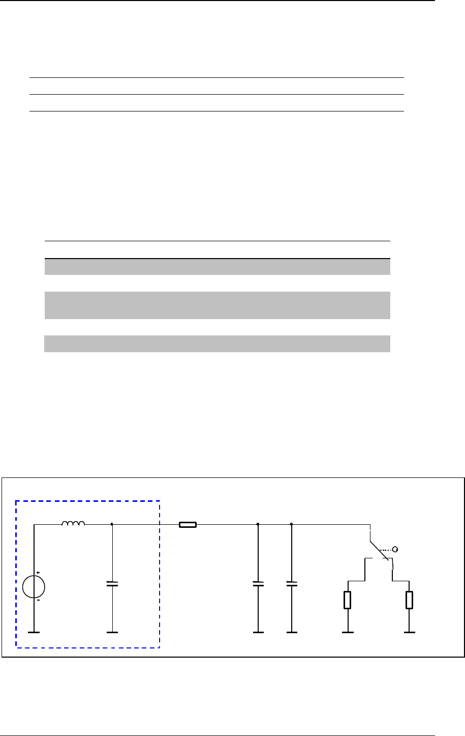
3.3.1 Power Supply (VCC)
The VCC supplies the module with external power. Any other voltage
needed is generated internally.
Parameter Mode Limit
Voltage to be applied Nominal 3.6 Volts
Tolerance 3.4 Volts - 4.0 Volts
Maximum voltage drop during
transmit burst 200mV
Over voltages 5.5 Volts
Current Drive capability at TX Full Power < 600 mA (average))
< 2 A (Peak)
GM 47/48 does not have internal capacitance to supply the large
current peaks during GSM transmission. Therefore on burst
transmission the application DC source is responsible for providing the
appropriate current.
Recommendations to the design of power supplies are given in the
following sections.
V1
3.6V
C1
220uF CF
100uF
Low ESR
CBULK
1000uF
Low ESR
RLINE
100mohm
RRX
120ohm
30mA Load
RTX
1.8ohm
2A Load
J1
577usec
1:8 Duty Cycle
'RLINE' represents resistance
of circuit between PSU and
GM47/GM48.
L1
33uH
+
+
+
2 Amp
Vcc
Figure 3.2 - Simplified Power Supply Reference Model
GM47/48 Design Guidelines
BA/SEM/MSC 02:0006 Rev PA1 11
3.3.2 General Recommendations
The power supply conditions for the GM47/48 Vcc connection are as
follows:
Maximum voltage drop during
transmit burst 200mV
Maximum Ripple TBD : [estimate 50mV]
Table 3.1
Recommended ESR on CBULK : <100mΩ
Recommended Maximum DC resistance between PSU and GM47 Vcc
: <200mΩ
Recommended minimum CBULK : 1000µF [see tables below]
The following tables provide a quick indication to recommended
CBULK capacitance to maintain Vcc drop <200mV for different PSU
current delivery and DC resistance between PSU and Module Vcc.
CBULK ESR = 50mΩ
RLINE = 50mΩ
PSU LIMIT CBULK (min) Transmit Burst
Vcc Dip (approx)
≥ 2.0 Amp 1000µF120mV
1.5 Amp *2500µF170mV
1.0 Amp *6000µF160mV
0.5 Amp *10000µF165mV
Table 3.2
CBULK ESR = 50mΩ
RLINE = 100mΩ
PSU LIMIT CBULK (min) Transmit Burst
Vcc Dip (approx)
≥ 2.0 Amp 1500µF200mV
1.5 Amp 4000µF150mV
1.0 Amp *6000µF170mV
0.5 Amp *10000µF180mV
Table 3.3
CBULK ESR = 50mΩ
RLINE = 150mΩ
PSU LIMIT CBULK (min) Transmit Burst
Vcc Dip (approx)
≥ 2.0 Amp 4000µF200mV
1.5 Amp 5000µF190mV
1.0 Amp *6000µF190mV
0.5 Amp *10000µF200mV
Table 3.4

GM47/48 Design Guidelines
BA/SEM/MSC 02:0006 Rev PA1 12
CBULK ESR = 50mΩ
RLINE = 200mΩ
PSU LIMIT CBULK (min) Transmit Burst
Vcc Dip (approx)
≥ 2.0 Amp 6000µF200mV
1.5 Amp 6000µF190mV
1.0 Amp 6000µF190mV
0.5 Amp *12000µF200mV
Table 3.5
Note: When this capacitance is used with the PSU conditions stated,
the PSU will reach current limit. Although this condition on Vcc will
not adversely affect the module performance, this may not be a
condition appropriate to the supply and may adversely affect other
devices sharing the PSU output. If the PSU cannot be driven to current
limit, please select a non-current limiting configuration of CBULK and
RLINE. It is the responsibility of the application developer to ensure
correct operation of the PSU.
Further details of the GSM burst transmission waveform are given in
appendix III.
3.3.3 On/Off signal
The on/off line should be attached to an open collector drive or
momentary contact switch otherwise the module alarm clock feature
will not operate. The on/off line is wired Red internally with the alarm
wake up signal.
GM47/48 Design Guidelines
BA/SEM/MSC 02:0006 Rev PA1 13
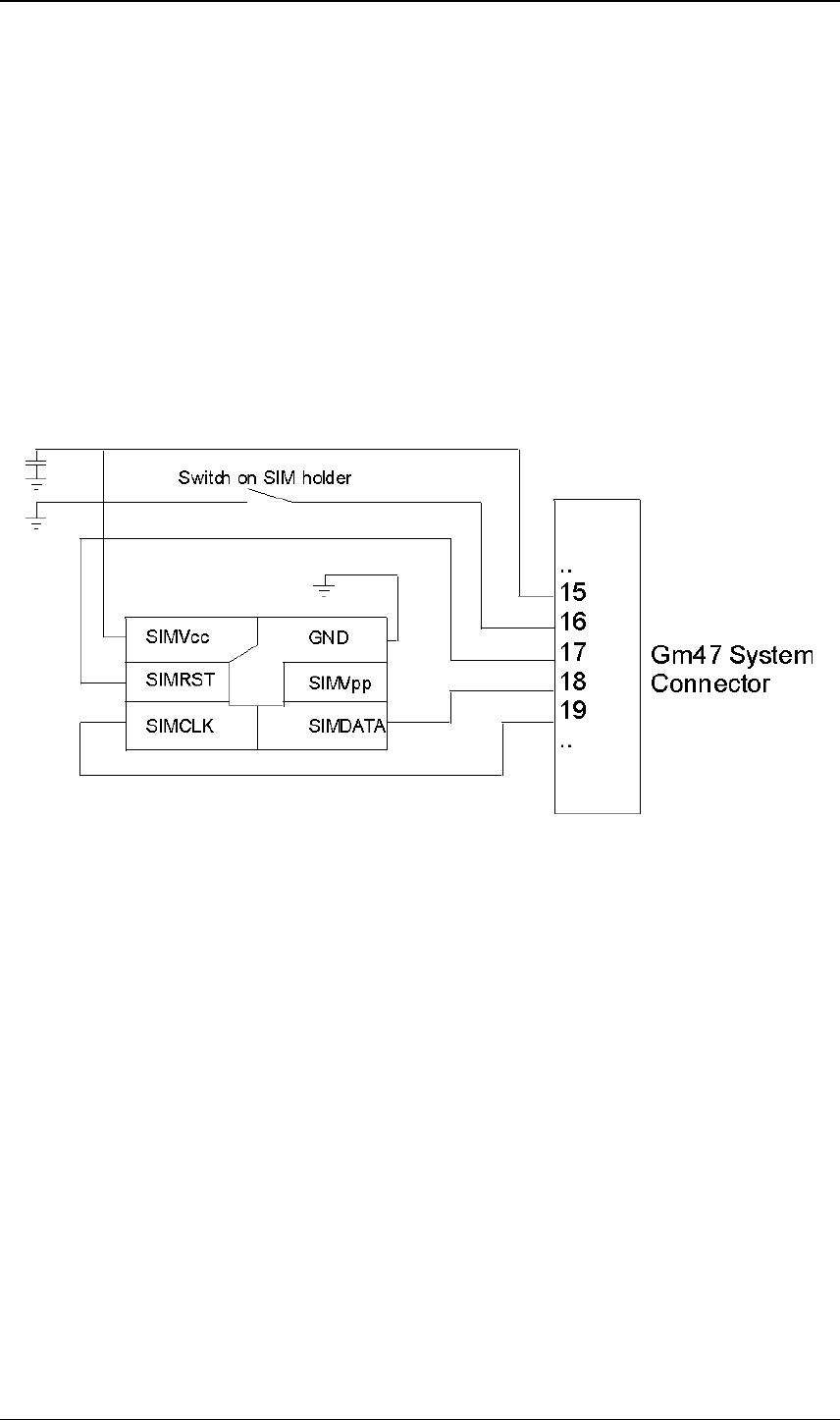
3.4 SIM connections
All track lengths between the SIM card and the module must be kept
below 15cm. This is due to the voltage drop/capacitance associated
with the extra track length and it has type approval issues as it will
affect timing.
This is primarily designed as a 3 Volts SIM interface, but if a 5 Volts
SIM card is connected to it the interface will automatically detect this
and adjust the appropriate parameters.
SIM connections are shown below.
Figure 3.2 SIM Connections
Points to note regarding SIM connection
• The SIM does not need protection between it and the module, if
protection is put in great care must be taken as SIM testing for
type approval is very sensitive to capacitance in the lines.
• De-coupling for Vcc is required, testing has been carried out
using a 2.2uF ceramic capacitor.
• It is recommended that SIM circuitry is run at the opposite end of
the module as a precaution.
GM47/48 Design Guidelines
BA/SEM/MSC 02:0006 Rev PA1 14
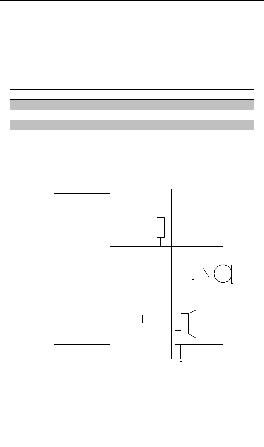
3.5 Audio Connections
Audio connections for both of the analogue paths are shown below.
3.5.1 Analogue Audio
Pin Signal Dir. Description
57 AFMS OAudio From Mobile Station
59 ATMS IAudio To Mobile Station
60 AGND -Ground (return) for analogue audio
ATMS and AFMS are the audio input and output for the module.
Figure 3.3 shows the connection of the analogue audio signals ATMS
and AFMS to the CODEC. An Advanced Portable Hands Free
accessory is also shown to clarify the connections.
Simplified Circuit
CODEC
ATMS
MIC
AGND
AFMS
Audio Out
<20 ohms
Bias
0V or 2V or 2.5V
Audio In
70K Ohms
2.7K
Switch
2.2u
Speaker
GM47
Figure 3.3. Analogue Audio Signal Connections.
It shall be possible to use the analogue audio signals in different modes.
• Hands-Free - This is the state referred to as Audio To Mobile
Station ATMS and Audio From Mobile Station AFMS, which

GM47/48 Design Guidelines
BA/SEM/MSC 02:0006 Rev PA1 15
will be used by audio accessories like handsets or Hands Free
equipment.
• Portable Hands Free - This state activates a different
amplification factor in the GM47 and activates a microphone bias
level of 2V in ATMS when a call is in progress.
This is the default state at power-on.
.
Audio Circuit Electrical characteristics
All sources must be AC-coupled except the Portable HandsFree
microphone, which shall be DC-coupled in order to supply DC current
to the Portable HandsFree microphone. AC coupling prevents incorrect
biasing or damage of the ATMS input. The capacitor must have a value
greater than shown below to avoid attenuation of low frequencies.
Application driving impedance (0.3 – 3.5 kHz) ≤ 300 Ω
AC coupling capacitance ≥ 1 µF
Module input impedance (0.3 – 3.5 kHz) > 50 kΩ
Low frequency cut-off. (-3 dB) 300 Hz ± 50 Hz
High frequency cut-off. (-3 dB) > 3500 ± 50 Hz
Hands-Free
mode 0V
Output DC bias level Portable
Hands Free
Mode
2.0V ± 0.1V
Additional Gain in Portable Hands Free Mode 28.5 dB
Table 1. ATMS Levels. Audio Levels
3.5.2 Advanced Portable Hands Free Functionality
This functionality consists in the detection of a push button press
connecting ATMS to AGND for a certain period of time. This will
create a change in the microphone DC bias level.
Microphone bias current at 2V1< 0.3 mA
Activated2< 100 Ω
DC impedance for push button Deactivated3> 10 kΩ [TBC]
Portable Handsfree electrical data
1 Bias current >0.7mA will cause false indication of button activation (Threshold is 100mV).
2 2V x ( 100 Ω / ( 2700 Ω + 100 Ω )) = 71 mV. Threshold is 100mV.
3 Lower impedance will reduce bias on microphone.

GM47/48 Design Guidelines
BA/SEM/MSC 02:0006 Rev PA1 16
AFMS is the analogue audio output from the module. When it is active,
the output is derived from the PCM digital audio by the decoder part of
the CODEC. The PCM data comes from PCMI on the system
connector.
It is also used as an ear-piece driver for the Portable Hands Free
accessory.
Zout4 (0.3 – 3.5 kHz) ≅ 120 Ω
Output capacitance 2.2 µF
Drive capability into 5 kΩ (0.3 – 3.5 kHz) > 2.4 Vpp [TBC]
Drive capability into1.5 kΩ (0.3 – 3.5 kHz) > 2.2 Vpp [TBC]
Levels5
(THD<5%)
Drive capability into 150 Ω (at 1 kHz) > 1.3 Vpp [TBC]
Table 2. AFMS Levels. Audio Levels
3.6 RF and antenna Integration
The rules for RF and antenna integration are general good practice
guidelines i.e.
• Ensure the antenna is a good 50Ω match across the GSM 900/1800
bands for GM47 and GSM 850/1900 bands for GM48.
• Antenna installation should be, where possible, not close to large
metal objects as this will affect the matching mentioned above.
• A specifically designed antenna for the GSM signals being
operated at will ensure the best reception.
If these are followed there should be no issues in terms of RF.
Please also see section 6.6 regarding SAR.
4 Output impedance includes impedance of EMC filter which is 100 Ω.
5 Need to check output drive levels with 100R EMI filter.
GM47/48 Design Guidelines
BA/SEM/MSC 02:0006 Rev PA1 17
3.7 Interfacing to a 3.3V µProcessor
Although the inputs to the modules can withstand a certain degree of
over voltage they should not be purposefully driven at a higher voltage
than that quoted in the pin out in appendix II.
This particularly applies to the serial com ports used to send and
receive the commands to and from the module. Level shifting I/C’s are
required to interface to the module.
An example of a suitable device is a Max3372 for level shifting, please
follow the below link for the data sheet. Note : ESD protection is not a
requirement for the level shifter.
http://pdfserv.maxim-ic.com/arpdf/MAX3372E-MAX3393E.pdf
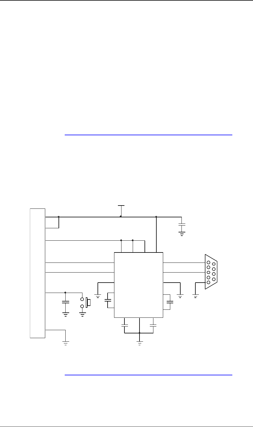
3.8 Software download and logging circuitry
Below the circuitry is shown which allows software download and
logging to be performed.
VCC 3V6
MAX3380E
VIO 2V7
CTMS
CFMS
VCC
0.1uF
1,3,5,7,9,11
2,4,6,8,10,12
34
58
45
46
SERVICE
14
0.1uF
ON/OFF
3
2
5
TD
RD
DTE
9 pin
D-Type
0.1uF
0.1uF
0.1uF
0.1uF
V
L
Fon
Foff
R1OUT
R1IN
T1IN
T1OUT
GND
V+
V-
+
+
+
+
C1+
C1-
C2+
C2-
15
19 13 20
17
5
11
4
8
12
3
218 6
1
GM47 SYSTEM CONNECTOR
9
T2IN
R2IN
14
The data sheet for the Maxim device can be found at
http://pdfserv.maxim-ic.com/arpdf/MAX3380E-MAX3381E.pdf

GM47/48 Design Guidelines
BA/SEM/MSC 02:0006 Rev PA1 18
4 Developers Board
The developers board is the reference design against which the module
has been type approved, the circuit diagram for this is available upon
request from customer support
4.1 Power Circuit
A 3A simple switcher step down voltage regulator has been used to
produce the module Vcc. Two 6800µF capacitors are located adjacent
to the module to cope with the GSM current pulses. The capacitors are
low ESR type approximately 16mΩ.
4.2 SIM Circuit
The SIM holder has been connected directly to the module, the
SIMVCC decoupling capacitor has been omitted and should be present
for all designs.
Note: Provision was made for additional ESD protection on the board
for development purposes.
This is not required and the devices have been removed from the
SIMDATA and SIMCLK signals to minimise capacitance on these
lines.
4.3 On/Off switch
The on/off line is connected to a momentary contact switch, this
ensures correct operation of the alarm clock feature in the module.
4.4 Programming circuitry
The data lines are converted between 2.7V & 5V logic and then
between 5V & RS232 levels. The data signal into the module is
powered from the VIO supply interface which ensures isolation of the
signal when the module is off.
To invoke programming mode the jumper JP27 is used. The Vppflash
signal path is no longer used.

GM47/48 Design Guidelines
BA/SEM/MSC 02:0006 Rev PA1 19
4.5 EMC
The circuit ground is bonded to the metal chassis of the developers kit
box, all signal connections are filtered via ferrite chokes.
4.6 Data signals:
The data and handshake lines are converted between 2.7V & 5V logic
and then between 5V & RS232 levels. The data signal and handshake
lines into the module are powered from the VIO supply interface which
ensures isolation of the signal when the module is off.
Diodes D3-5,D7 & D8 are not fitted.

GM47/48 Design Guidelines
BA/SEM/MSC 02:0006 Rev PA1 20
5 Part numbers
5.1 System connector
A connector that can be used to interface to the system connector is the
Samtech FLE or SFMC or CLP series, the female part number is CLP-
130-02-F-D.
This connector or an equivalent can be sourced from imperial
connectors below, again this company is just an example of one
supplier.
5.2 RF connector
MMCX is a standard RF connector and should be able to be sourced
from most suppliers.
5.3 SIM card holder
The data sheet for the SIM holder that is used on the developers board
is available on request from customer support.
The card holder is a lockable type as problems have been experienced
in the past with the slide in holders.
5.4 Suppliers
Below are listed suppliers of connectors which SonyEricsson uses, the
quality or availability of components cannot be guaranteed.
5.4.1 Imperial connectors
Imperial connectors have a good selection of SIM holders, the MMCX
RF connector and the system connector.
SIM card reader
For the SIM card reader follow the link
http://www.imperial-connect.co.uk/products/sim.html

GM47/48 Design Guidelines
BA/SEM/MSC 02:0006 Rev PA1 21
System connector
For the system connector follow
http://www.imperial-connect.co.uk/products/prodprofile127.html
click on ITRQPGA thumbnail.
5.4.2 IMS connectors
Connector cables from MMCX to SMA can be ordered from this
supplier normally with a 2-3 week lead time.

GM47/48 Design Guidelines
BA/SEM/MSC 02:0006 Rev PA1 22
6 Type Approval
The system integrator has to get CE marking for the integrated solution
with the GSM module in Europe (GM47) and the FCC approval in the
US (GM48). The system integrator only has to show compliance with
the essential requirements of the module by the integration of it into the
application.
If the external elements are designed according to the guidelines of this
document the testing would be the following:
• Integration with GM47
• EMC in all modes of operation
• Safety
• Integration with the GM48
• FCC approvals of all applicable parts
Sony Ericsson recommends that all these tests are performed by the
customer in an accredited test house. After that, all documentation
together with the test reports and certificates of the application should
be sent to Sony Ericsson in order to register the application to the
accessories list for the approval of the module, this will aid the
approval of the application world wide.
6.1 Documentation required
The system integrator is required to produce a document which will be
submitted to the test house containing the following information.
• Summary of the application
• Hardware description
• Block diagram with an explanation
• Schematics
• PCB/Component layout
• Bill of materials
This documentation will also be required for Sony Ericsson to add the
application to the list of approved accessories for the module in
addition to the test reports and certificates obtained from the test house.
6.2 Power supply
It is essential the application power supply is designed to comply with
the specification in section 3. This will be sufficient to pass type
approval, no RF testing will be required if it meets these specifications.

GM47/48 Design Guidelines
BA/SEM/MSC 02:0006 Rev PA1 23
6.3 SIM Testing
SIM testing does not need to be carried out since it is a passive
component. Points to note regarding the implementation of the SIM
card holder are as follows.
• SIM presence must be implemented to comply with the module
approval conditions.
• Any manufacturers SIM card holder can be used and this can also
be either 6 or 8 pins.
6.4 EMC/ESD & Safety
EMC and safety tests according to the ITU/GSM and FCC standards
will have to be completed as part of the mandatory testing. The GM
47/48 were originally type approved outside of a metal box. Additional
shielding is not strictly required the external application. This is the
responsibility of the system integrator. Overall ESD protection should
be guaranteed by the system integrator.
The EMC standard which the application must be tested to is EN 301
489-7, this can be found at the following web site.
http://www.etsi.org/getastandard/home.htm
The safety standard which the application must be tested to is EN
60950, the can be found at the following web site
http://www.iec.ch/
For the GM48 FCC part 15 regulations, these can be found at
http://www.fcc.gov/
6.5 RF Testing
6.5.1 GM47
As long as the antenna connected to the module is of the correct
impedance as specified in section 3.7 and is passive further RF testing
for TA is not required. Although it should be noted that radiation
performance is the responsibility of the system integrator.
6.5.2 GM48
According to the US rules (GM48) any change in RF path i.e. the
antenna path will require new approval according to FCC part 22 and
24.

GM47/48 Design Guidelines
BA/SEM/MSC 02:0006 Rev PA1 24
6.6 SAR warning
If the application is using an antenna which is less than 20cm away
from the any part of the users body, integrators are legally obliged to
publish SAR figures for the product. This testing would need to be
carried out by the system integrator.
Even if SAR measurements are not required it is considered good
practice to insert a warning in any manual produced indicating it is a
radio product and that care should be taken.
6.7 Other TA issues
6.7.1 External Application software
If the software of the external application is changed it has no effect
upon the type approval certificate issued to it.
6.7.2 GM47 software updates
If the GM47 software is updated there should be no further action
required by the system integrator as accessories lists are generally
carried across between TA certificates and any software supplied by
Sony Ericsson will be fully Type Approved.

GM47/48 Design Guidelines
BA/SEM/MSC 02:0006 Rev PA1 25
Appendix I - Technical Data
Mechanical specifications
Maximum length: 50 mm
Maximum width: 33 mm
Maximum thickness: 6.82 mm (without system connector pins length)
Weight: 18,5 g
Power supply voltage, normal operation
Voltage: 3.6V Nominal
Tolerance ±0.2V
Ripple: <100mV @ 200KHz, <20mV @>200KHz
Voltage must always stay within a normal operating range, ripple included.
Power consumption: Speech mode < 600 mA (< 2 A peak)
Idle mode: 5 mA
Switched off: < 100 µA
Radio specifications
Frequency range: GM 47: EGSM 900 MHz and 1800 MHz (Dual Band)
GM 48: GSM 850 MHz and 1900 MHz (Dual Band)
Maximum RF output power: 2 W / 1 W
Antenna impedance: 50 Ω
SIM card
SIM card interface: 3 V or 5 V
Support of external SIM card
Environmental specifications
Operating temperature range: -25 0C to +55 0C
Storage temperature range: -40 0C to +85 0C
Maximum relative humidity: 95% at +40 0C
Stationary vibration, sinusoidal: Displacement: 7.5 mm Acceleration amplitude: 20 m/s2 40
m/s2 Frequency range: 2-8 Hz 8-200 Hz 200-500 Hz
Stationary vibration, random Acceleration spectral density (m2/s2): 0.96 2.88 0.96
Frequency range: 5-10 10-200 200-500 60 min per/axis
Non-stationary vibration, including
shock Shock response spectrum I, peak acceleration: - 3 shocks in
each axis and direction: 300 m/s2, 11 ms

GM47/48 Design Guidelines
BA/SEM/MSC 02:0006 Rev PA1 26
Shock response spectrum II, peak acceleration: - 3 shocks in
each axis and direction: 1000 m/s2, 6 ms
Bump: Acceleration 250 m/s2
Free fall transportation: 1.2 m
Rolling pitching transportation: Angle: ±35 degrees, period: 8s
Static load: 10 kPa
Low air pressure/high air pressure: 70 kPa / 106 kPa
Storage
SMS Storage capacity 40 in ME
Upto 25 on SIM (SIM dependent)
Phone book capacity 100
DAC
Parameter Value Units
Resolution 8bit
Output voltage swing for Code=00HEX 0.138 ± 0.1 V
Output voltage swing for Code=FFHEX 2.61 ± 0.2 V
Nominal Step Size 9.668 ± 0.1 mV
Linear Code Range 8-247 (8H-F7H)LSB
Absolute Error during Linear Range ±100 mV
Conversion Speed <100 µs
ADC
Parameter Value Units
Resolution 8bit
Input voltage for Code=00H0.01 ± 0.01 V
Input voltage for Code=FFH2.75 ± 0.1 V
Nominal Step Size 10.742 mV
Accuracy ±3LSB
Input Impedance >1 MΩ
Conversion Time to within 0.5bit <100 µs

GM47/48 Design Guidelines
BA/SEM/MSC 02:0006 Rev PA1 27
Appendix II – GM47/48 Pin out
Pin Signal Name Dir Signal Type Description
1. VCC -Supply Power Supply
2. DGND - - Digital Ground
3. VCC -Supply Power Supply
4. DGND - - Digital Ground
5. VCC -Supply Power Supply
6. DGND - - Digital Ground
7. VCC -Supply Power Supply
8. DGND - - Digital Ground
9. VCC -Supply Power Supply
10. DGND - - Digital Ground
11. VCC -Supply Power Supply
12. DGND - - Digital Ground
13. Reserved for future use
14. ON/OFF IInternal pull up,
open drain Turns the module on/off
Former WAKE_B
15. SIMVCC -Dig. 3/5 V SIM card power supply
Power output for SIM Card from module
16. SIMPRESENCE IInternal pull up,
open drain SIM Presence
A "1" shall indicate that the SIM is missing;
a "0" that it is inserted.
17. SIMRST ODig. 3/5 V SIM card reset
18. SIMDATA I/O Dig. 3/5 V SIM card data
19. SIMCLK ODig. 3/5 V SIM card clock
20. DAC OAnalogue Digital to Analogue converter
21. IO1 I/O Digital, 2.75 General purpose input/output 1
22. IO2 I/O Digital, 2.75 General purpose input/output 2
23. IO3 I/O Digital, 2.75 General purpose input/output 3
24. IO4 I/O Digital, 2.75 General purpose input/output 4
25. VRTC ISupply 1.5 V Voltage for real time clock
26. ADC1 IAnalogue Analogue to Digital converter 1
27. ADC2 IAnalogue Analogue to Digital converter 2
28. ADC3 IAnalogue Analogue to Digital converter 3
29. SDA I/O 2.75, internal
pullup I2C Data
30. SCL O2.75, internal
pullup I2C Clock
31. BUZZER ODig. 2.75 Buzzer output from module

GM47/48 Design Guidelines
BA/SEM/MSC 02:0006 Rev PA1 28
32. TIMESTAMP ODig. 2.75 Timestamp
Timestamp is reserved for future use, if A-
GPS is implemented on network side.
33. LED ODig. 2.75 Flashing LED
34. VIO OPower Out 2.75 Module powered indication.
The VIO is a 2.75 V output that could
power external devices to transmit data
towards the GSM device to a 75mA max.
35. TX_ON ODig 2.75 This output shall indicate when the GSM
module is going to transmit the burst.
36. RI ODig. 2.75 Ring Indicator
37. DTR IDig. 2.75 Data Terminal Ready
38. DCD ODig. 2.75 Data Carrier Detect
39. RTS IDig. 2.75 Request To Send
40. CTS ODig. 2.75 Clear To Send
41. TD IDig. 2.75 Transmitted Data
Data from DTE (host) to DCE (module).
[former DTMS]
42. RD ODig. 2.75 Received Data
Data from DCE (module) to DTE (host).
[former DFMS]
43. TD3 IDig. 2.75 UART3 Transmission
Data from DTE (host) to DCE (module).
[former DTMS]
44. RD3 ODig. 2.75 UART3 Reception
Data from DTE (host) to DCE (module).
[former DTMS]
Data from DCE (module) to DTE (host).
[former DFMS]
45. TD2 IDig. 2.75 UART2 Reception
Former CTMS. Used for flashing
46. RD2 ODig. 2.75 UART2 Transmission
Data from DCE (module) to DTE (host).
[former DFMS]
Former CFMS. Used for flashing
47. PCMULD IDig. 2.75 DSP PCM digital audio input
48. PCMDLD ODig. 2.75 DSP PCM digital audio output
49. PCMO ODig. 2.75 Codec PCM digital audio output
50. PCMI IDig. 2.75 Codec PCM digital audio input
51. PCMSYNC ODig. 2.75 DSP PCM frame sync
52. PCMCLK ODig. 2.75 DSP PCM clock output
53. MICP IAnalogue Microphone input positive
54. MICN IAnalogue Microphone input negative
55. BEARP OAnalogue Speaker output positive

GM47/48 Design Guidelines
BA/SEM/MSC 02:0006 Rev PA1 29
56. BEARN OAnalogue Speaker output negative
57. AFMS OAnalogue Audio output from module
58. SERVICE I12V/2.7V Flash programming voltage for the MS.
Enable logger information if no flashing
Former VPPFLASH
59. ATMS IAnalogue Audio input to module
60. AGND - - Analogue ground
GM47/48 Design Guidelines
BA/SEM/MSC 02:0006 Rev PA1 30
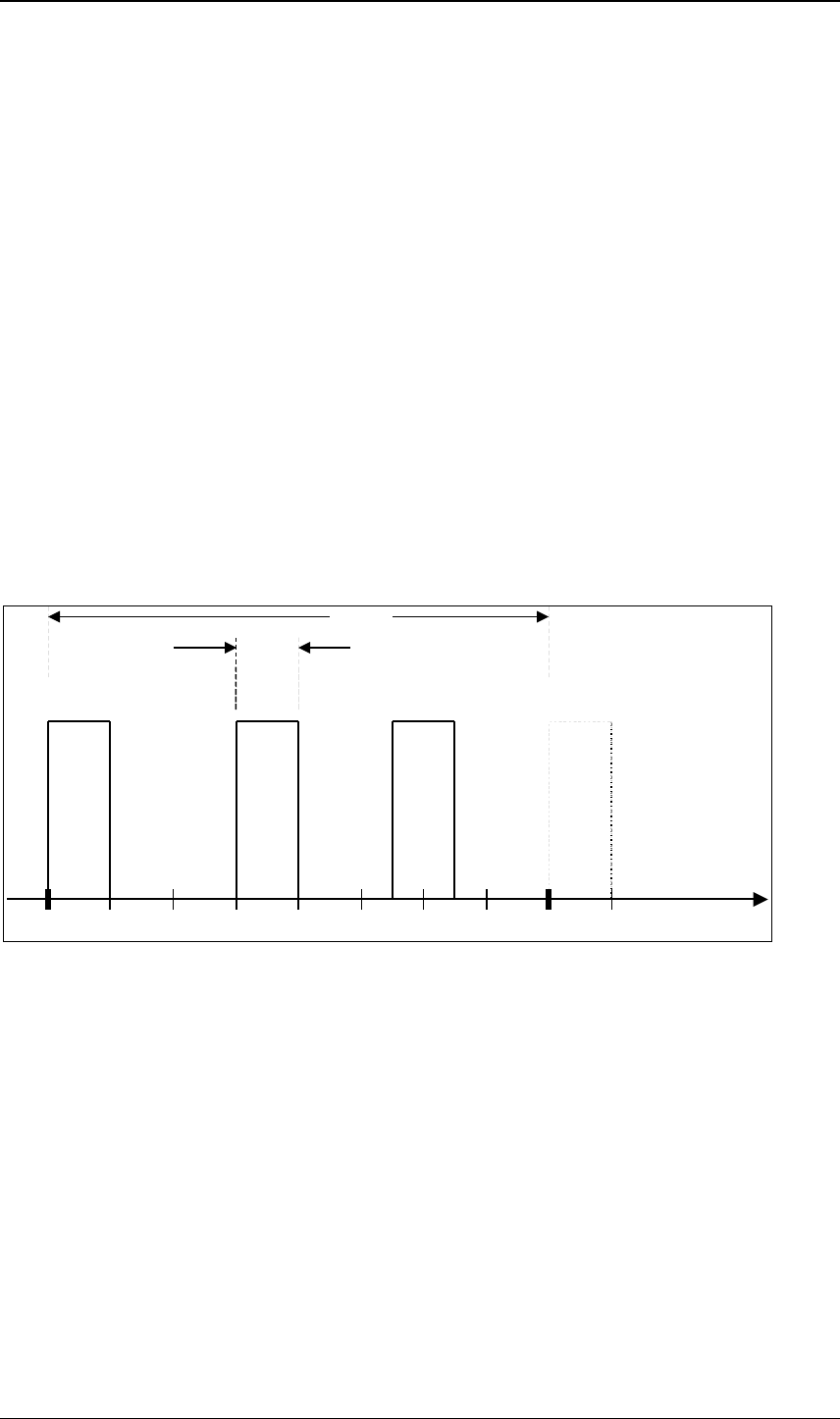
Appendix III GSM transmit waveform characteristics
The simplified GSM loading characteristics and power supply reference
model in relation to the GM47 system connector is represented in
figure 1. J1 represents the interface to the GM47 system connector and
the voltage there is referenced Vcc.
Figure 2 shows a 1:8 cycle with the receive burst occurring in timeslot
1 and transmit in timeslot 6. Some of the quiet period is used by the
module to ‘listen’ to other GSM base-stations.
In simple terms the module can draw up to 2 Amps during the transmit
burst. The receive burst can draw up to 100mA. As the current
consumption of the receive burst does not normally cause problems for
power supply current drain, the simplified PSU model in figure 1
combines the receive, monitor and idle frames into an average current
consumption around 30mA. The transmit burst requires special
attention.
1 2 3 4 5 6 7 8 1 2
Receive Transmit Monitor Receive
577 µs
4.6 ms
timeslot
Figure 1 - Simplified GSM Timing Diagram
There are three main areas to consider in order to meet the transmit
burst requirements: PSU current capability, resistance between the
supply and module (RLINE), and bulk capacitance (CBULK) at the module
Vcc connection. The effect that each of these parameters has on the
waveform shape at Vcc is indicated in figure 3.
GM47/48 Design Guidelines
BA/SEM/MSC 02:0006 Rev PA1 31
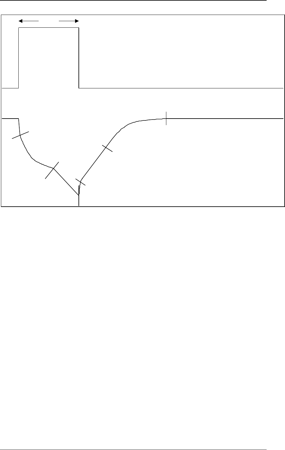
A
B
CD
E
FG
577 µs
TRANSMIT
GM47 Vcc
Figure 2 - Transmit Burst Vcc Waveform
A. The sharp fall in voltage in this region is caused by the ESR
of the capacitors (mounted as close to the module Vcc pins
as possible.
B. The RC discharge is controlled by CBULK, RLINE, and RTX.
C. If the PSU cannot supply the 2A max load of the GM47 and
current limit is reached the discharge of CBULK goes linear.
If current limit is not reached then section ‘B’ will continue for
the length of the transmit burst. Current limit will be reached
when the voltage dropped across RLINE reaches V = ILIM *
RLINE.
D. The sharp fall in voltage in this region is again caused by the
ESR of the capacitors.
E. CBULK will charge linearly while the supply is in current limit.
This section is not relevant while the PSU is not current
limited.
F. The RC charge is controlled by CBULK and RLINE.
G. Once the transmit burst is finished, the 1:8 duty cycle should
ensure that there is sufficient time for the PSU to fully
recover before the next transmit burst.