Sony 6220501-BV Transmitter module for mobile applications User Manual Exhibit 08 Manual
Sony Mobile Communications Inc Transmitter module for mobile applications Exhibit 08 Manual
Sony >
Contents
- 1. Exhibit 08 Manual
- 2. Exhibit 8 Design Guidelines
- 3. Exhibit 8 Integrators Manual
- 4. revised page
Exhibit 08 Manual

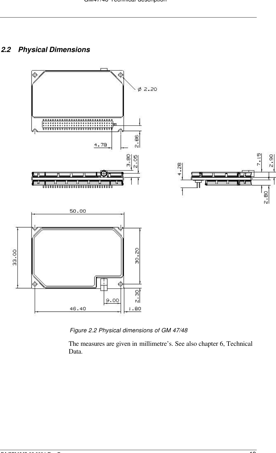
![GM47/48 Technical descriptionBA/SEM/MS 02:0004 Rev B1533. LED ODig. 2.75 Flashing LED34. VIO OPower Out 2.75 Module powered indication.The VIO is a 2.75 V output that couldpower external devices to transmit datatowards the GSM device to a 75mA max.35. TX_ON ODig 2.75 This output shall indicate when the GSMmodule is going to transmit the burst.36. RI ODig. 2.75 Ring Indicator37. DTR IDig. 2.75 Data Terminal Ready38. DCD ODig. 2.75 Data Carrier Detect39. RTS IDig. 2.75 Request To Send40. CTS ODig. 2.75 Clear To Send41. TD IDig. 2.75 Transmitted DataData from DTE (host) to DCE (module).[former DTMS]42. RD ODig. 2.75 Received DataData from DCE (module) to DTE (host).[former DFMS]43. TD3 IDig. 2.75 UART3 TransmissionData from DTE (host) to DCE (module).[former DTMS]44. RD3 ODig. 2.75 UART3 ReceptionData from DTE (host) to DCE (module).[former DTMS]Data from DCE (module) to DTE (host).[former DFMS]45. TD2 IDig. 2.75 UART2 ReceptionFormer CTMS. Used for flashing46. RD2 ODig. 2.75 UART2 TransmissionData from DCE (module) to DTE (host).[former DFMS]Former CFMS. Used for flashing47. PCMULD IDig. 2.75 DSP PCM digital audio input48. PCMDLD ODig. 2.75 DSP PCM digital audio output49. PCMO ODig. 2.75 Codec PCM digital audio output50. PCMI IDig. 2.75 Codec PCM digital audio input51. PCMSYNC ODig. 2.75 DSP PCM frame sync52. PCMCLK ODig. 2.75 DSP PCM clock output53. MICP IAnalogue Microphone input positive54. MICN IAnalogue Microphone input negative55. BEARP OAnalogue Speaker output positive56. BEARN OAnalogue Speaker output negative57. AFMS OAnalogue Audio output from module](https://usermanual.wiki/Sony/6220501-BV.Exhibit-08-Manual/User-Guide-237162-Page-15.png)
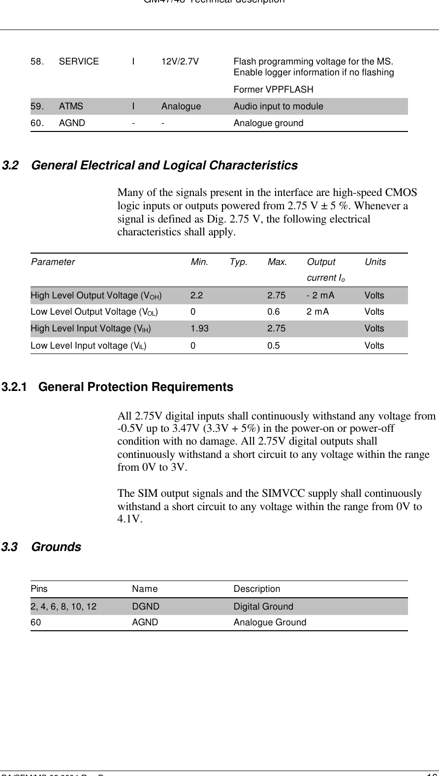
![GM47/48 Technical descriptionBA/SEM/MS 02:0004 Rev B223.6.2 Audio From Mobile Station (AFMS)AFMS is the analogue audio output from the module. When it isactive, the output is derived from the PCM digital audio by thedecoder part of the CODEC. The PCM data comes from PCMI on thesystem connector. It is also used as an ear-piece driver for the PortableHands Free accessory.Parameter LimitSpeaker impedance 64 Ω το 1ΚΩAFMS Output Capacitance 2.2 µF ±10%Levels (THD < 5 %) Drive capability into 5 kΩ (0.3 -3.5 kHz)> 2.4 Vpp [TBC]Drive capability into 1.5 kΩ (0.3 -3.5 kHz) > 2.2 Vpp [TBC]Drive capability into 150 Ω (at1kHz)> 1.3 Vpp [TBC]3.7 Microphone SignalsPin Speaker signals Dir Function53 MICP IMicrophone Positive Input54 MICN IMicrophone Negative InputMICP and MICN are the microphone-input pins. These inputs shall becompatible with an electret microphone. The microphone contains aFET buffer with open drain output, which must be supplied at least+2V relative to ground.Figure 3.3 Microphone connection to moduleCCO is the source voltage that will provide the necessary drivecurrent for the microphone.](https://usermanual.wiki/Sony/6220501-BV.Exhibit-08-Manual/User-Guide-237162-Page-22.png)