Sony 6220501-BV Transmitter module for mobile applications User Manual Exhibit 08 Manual
Sony Mobile Communications Inc Transmitter module for mobile applications Exhibit 08 Manual
Sony >
Contents
- 1. Exhibit 08 Manual
- 2. Exhibit 8 Design Guidelines
- 3. Exhibit 8 Integrators Manual
- 4. revised page
Exhibit 08 Manual

GM 47/GM 48
Technical Description

CE
The product described in this manual conforms to the Radio and Teleterminals directive 1999/5/EC with
requirements covering EMC directive 89/336/EEC and Low Voltage directive 73/23/EEC.
SAR statement: This product is intended to be used with the antenna or other radiating element 20 cm far
away of the any part of the human body.
The information contained in this document is the proprietary information of Sony Ericsson Mobile
Communications. The contents are confidential and any disclosure to persons other than the officers,
employees, agents or subcontractors of the owner or licensee of this document, without the prior written
consent of Sony Ericsson Mobile Communications, is strictly prohibited.
Further, no portion of this publication may be reproduced, stored in a retrieval system, or transmitted in
any form or by any means, electronic or mechanical, including photocopying and recording, without the
prior written consent of Sony Ericsson Mobile Communications, the copyright holder.
Second edition (February 2002)
Sony Ericsson Mobile Communications. publishes this manual without making any warranty as to the
content contained herein. Further Sony Ericsson Mobile Communications. reserves the right to make
modifications, additions and deletions to this manual due to typographical errors, inaccurate information,
or improvements to programs and/or equipment at any time and without notice. Such changes will,
nevertheless be incorporated into new editions of this manual.
All rights reserved.
©Sony Ericsson Mobile Communications., 2002
Publication number:
Printed in UK
Trademarks
AIX is a trademark owned by International Business Machines Corporation

GM47/48 Technical description
BA/SEM/MS 02:0004 Rev B
3
Contents
1INTRODUCTION ...........................................................................................................5
1.1 OVERVIEW ...............................................................................................................5
1.2 FEATURES................................................................................................................6
1.2.1 Type of Mobile Station ......................................................................................6
1.2.2 SMS ................................................................................................................7
1.2.3 Voice calls .......................................................................................................7
1.2.4 Data.................................................................................................................7
1.2.5 SIM Card..........................................................................................................8
1.2.6 Power consumption ..........................................................................................8
1.2.7 Other features ..................................................................................................8
1.2.8 Development Kit...............................................................................................8
1.3 PRECAUTIONS...........................................................................................................9
1.4 ABBREVIATIONS ........................................................................................................9
2MECHANICAL DESCRIPTION.....................................................................................11
2.1 INTERFACE DESCRIPTION..........................................................................................11
2.2 PHYSICAL DIMENSIONS.............................................................................................12
3SYSTEM CONNECTOR INTERFACE...........................................................................13
3.1 OVERVIEW .............................................................................................................13
3.2 GENERAL ELECTRICAL AND LOGICAL CHARACTERISTICS................................................16
3.2.1 General Protection Requirements....................................................................16
3.3 GROUNDS ..............................................................................................................16
3.3.1 The Analogue Ground.....................................................................................17
3.3.2 The Digital Ground (DGND).............................................................................17
3.4 REGULATED POWER SUPPLY ....................................................................................17
3.4.1 Power Supply (VCC).......................................................................................18
3.5 ON/OFF AND EXTERNAL POWER SIGNALS..................................................................18
3.5.1 Module ON/OFF.............................................................................................18
3.5.2 External 2.75 V (VIO)......................................................................................19
3.6 ANALOGUE AUDIO ...................................................................................................19
3.6.1 Audio To Mobile Station (ATMS)......................................................................20
3.6.2 Audio From Mobile Station (AFMS)..................................................................22
3.7 MICROPHONE SIGNALS ............................................................................................22
3.8 SPEAKER SIGNALS ..................................................................................................23
3.9 DIGITAL AUDIO ........................................................................................................23
3.10 SERIAL DATA..........................................................................................................24
3.10.1 UART 1 (RS232) - RD, TD, RTS, CTS, DTR, DCD and RI.................................26
3.10.2 Serial Data Signals - RD, TD...........................................................................26
3.10.3 Control Signals - RTS, CTS, DTR, DCD, RI......................................................27
3.10.4 UART 2 - TD2, RD2........................................................................................29
3.10.5 UART 3 - TD3, RD3........................................................................................29
3.11 SIM CARD RELATED SIGNALS....................................................................................30
3.11.1 SIM Detection – SIM Presence........................................................................31
3.12 SERVICE/PROGRAMMING ..........................................................................................31
3.13 BUZZER .................................................................................................................32
3.14 LED......................................................................................................................32
3.15 TX_ON - BURST TRANSMISSION ...............................................................................33
3.16 TIMESTAMP ............................................................................................................33
3.17 REAL TIME CLOCK...................................................................................................34
4ANTENNA CONNECTOR............................................................................................35

GM47/48 Technical description
BA/SEM/MS 02:0004 Rev B
4
5AT COMMAND SUMMARY..........................................................................................36
6TECHNICAL DATA.....................................................................................................39

GM47/48 Technical description
BA/SEM/MS 02:0004 Rev B
5
1 Introduction
1.1 Overview
The GM47/48 belong to a new generation of Sony Ericsson Mobile
Communications GSM modules. This document describes the main
characteristics and functionality of the GM 47/48, two dual band
products for 900/ 1800 MHz and 850/1900 MHz GSM bands
respectively.
They are intended to be used in both machine-to-machine applications
and man-to-machine applications. The module serves its purpose
when there is a need for sending and receiving data (by SMS, CSD,
HSCSD, or GPRS), as well as making voice calls over the GSM
network.
GM47/48 are business-to-business products. It is intended to be sold
to manufacturers, system integrators, applications developers-
developing solutions with wireless communication. The module is
intended to be integrated by the system integrator within an
application. The module and the external application will form a
system for wireless communication.
A typical system is one where a micro controller in an external
application communicates with the module over its serial interface.
The micro controller will control the module, via the supported set of
AT commands. It is assumed that the system integrators have a high
technical knowledge and the ability to integrate the module into a
system. For the GM47/48 modules some interesting applications are
the following:
• Fleet and Asset Management
• Vending Machines
• Security and Alarm
• Other telemetry applications

GM47/48 Technical description
BA/SEM/MS 02:0004 Rev B
6
1.2 Features
The module performs a set of telecom services (TS) according to
GSM standard phase 2+, ETSI and ITU-T. The functions of the
module are implemented by issuing AT commands over the serial
interface. Supported AT commands are listed in section 5, these are
defined further in GSM 7.05.
1.2.1 Type of Mobile Station
The GM 4X family are normal dual band type of MS with the
following characteristics.
GM 47 GSM 900 E-GSM 900 GSM 1800
Frequency Range
(MHz) TX: 890-915
RX: 935-960
TX: 880-890
RX: 925-935
TX: 1710-1785
RX: 1805-1880
Channel spacing 200 kHz 200 kHz
Number of channels 173 Carriers *8 (TDMA)
GSM: Channels 1 to 124
E-GSM: Channels 975 to 1023
374 Carriers *8 (TDMA)
DCS: Channels 512 to 885
Modulation GMSK GMSK
TX Phase Accuracy < 5º RMS Phase error (burst) < 5º RMS Phase error (burst)
Duplex spacing 45 MHz 95 MHz
Receiver sensitivity at
antenna connector < - 102 dBm < - 102 dBm
Transmitter output
power at antenna
connector
Class 4
2W (33 dBm)
Class 1
1W (30 dBm)
Automatic hand-over between GSM 900 and GSM 1800
GM 48 GSM 850 GSM 1900
Frequency Range (MHz) TX: 824-849
RX: 869-894
TX: 1850-1910
RX: 1930-1990
Channel spacing 200 kHz 200 kHz
Number of channels 123 carriers *8 (TDMA)
GSM: Channels 128 to 251
298 Carriers *8 (TDMA)
PCS: Channels 512 to 810
Modulation GMSK GMSK
TX Phase Accuracy < 5º RMS Phase error (burst) < 5º RMS Phase error (burst)
Duplex spacing 45 MHz 80 MHz
Receiver sensitivity at antenna
connector < - 102 dBm < - 102 dBm
Transmitter output power at
antenna connector Class 5
0.8 W (29 dBm)
Class 1
1W (30 dBm)

GM47/48 Technical description
BA/SEM/MS 02:0004 Rev B
7
Automatic hand-over between GSM 850 and GSM 1900
1.2.2 SMS
The module supports the following SMS services:
• Sending: MO, both PDU and Text mode supported.
• Receiving: MT, both PDU and Text mode supported.
• CBM is a service, in which a message is sent to all subscribers
located in one or more specific cell(s) in the GSM network, for
example, cell location information.
• SMS STATUS REPORT according to GSM 03.40.
• SMS COMMAND according to GSM 03.40.
The maximum length of an SMS message is 160 characters when
using 7-bit encoding. For 8-bit data, the maximum length is 140 bytes.
The module does support upto 6 concatenated messages to extend this
function.
1.2.3 Voice calls
The GM47/48 offers the capability of MO and MT voice calls, as well
as supporting emergency calls. In addition to this multiparty, call
waiting and call deflection features are available. Some of these
features are operator specific.
The module offers normal analogue input/output lines, analogue audio
input/ output lines in differential modes, and digital audio interface,
with the possibility of accessing internal points within the digital
audio lines. Moreover, the GM 47/GM48 has embedded echo
canceller and noise suppresser, which provides high quality audio.
The module supports both HR, FR and EFR voice coding, provided
that EFR is available in the network.
1.2.4 Data
The module supports the following data protocols:
• General Packet Radio Service (GPRS). The modules are Class B
Terminals, which provides simultaneous activation and attach of
GPRS and GSM services. The GM47/48 modules are GPRS 3+1
devices, which are capable of transmitting in one timeslot per
frame (uplink), and receiving in a maximum of three timeslots per
frame (downlink).
• Circuit Switched Data (CSD). GM47/48 modules are capable to
stablish a circuit switch data communication at 9.6 kbps, V42bis
compression is not supported.

GM47/48 Technical description
BA/SEM/MS 02:0004 Rev B
8
• High Speed Circuit Switched Data (HSCSD). GM47/48 support
HSCSD communication, with one timeslot per frame capacity in
the uplink and two timeslots per frame capacity in the downlink
(2+1).
1.2.5 SIM Card
The module supports the connection of an external SIM Card with 3V
and 5 V technology, via the 60-pin system connector. The module
does not have an internal SIM holder.
1.2.6 Power consumption
Stand-by1Transmit/Operation
GSM 850 & 900 MHz 20 mA 275 mA (2A peak)
GSM 1800 & 1900 MHz 20 mA 250 mA (1.75A peak)
Note! The power consumption during transmission is measured at
maximum transmit power.
1.2.7 Other features
• Internet Ready Module
• 07.10 Multiplexing
• Bluetooth interoperability
• GPS interoperability
• SIM application toolkit, class 2 release 96 compliant
1.2.8 Development Kit
Sony Ericsson Mobile Communications provides the opportunity to
test the module in a limited scale, before ordering a large quantity.
With the development kit you can quickly get started with the module.
The kit includes necessary accessories (software and hardware) that
you will need for your test purposes. It also includes the following:
• GSM module GM 47 or GM 48
• Integrator’s Manual
• Warranty Sheet
1This figures are tentative data, subject to change.

GM47/48 Technical description
BA/SEM/MS 02:0004 Rev B
9
The Integrator’s Manual provides you with all the information you
need to be able to integrate the module with your application.
1.3 Precautions The GM47/48 should be handled like any mobile station. In the
Integrators’ Manual you will find more information about safety and
product care. In the Technical Data chapter in this document the
environmental and electrical limits are specified. Never exceed these
limits to ensure the module is not damaged.
1.4 Abbreviations
Abbreviation Explanation
BT Bluetooth
CBS Cell Broadcast Service
CBM Cell Broadcast Messaging
CSD Circuit Switch Data
DCE Data Circuit Terminating Equipment
DTE Data Terminal Equipment
DTMF Dual Tone Multi Frequency
EFR Enhanced Full Rate codec
EMC Electro-Magnetic Compatibility
ETSI European Telecommunications Standards Institute
FR Full Rate codec
GPRS General Packet Radio Service
GPS Global Positioning System
GSM Global System for Mobile Comunication
HR Half Rate codec
HSCSD High Speed Circuit Switched Data
ITU-T International Telecommunication Union – Telecommunications
Standardisation Sector
ME Mobile Equipment
MO Mobile Originated
MS Mobile Station
MT Mobile Terminated
PCM Pulse Code Modulation
PDU Protocol Data Unit
RLP Radio Link Protocol
RF Radio Frequency
RTC Real Time Clock

GM47/48 Technical description
BA/SEM/MS 02:0004 Rev B
10
SDP Service Discovery Protocol
SMS Short Message Service
SIM Subscriber Identity Module
TBD To Be Defined
GM47/48 Technical description
BA/SEM/MS 02:0004 Rev B
11
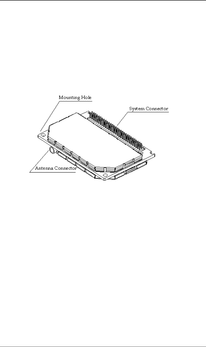
2 Mechanical Description
2.1 Interface Description
The picture below presents the conceptual mechanical design of the
GM 47/48. The GM 47/48 are protected with AISI 304 Stainless Steel
covers suitable to fulfil the environmental and EMC requirements.
Dimensions, the position of the different connectors and mounting
holes are shown in figure 2.2.
Figure 2.1 GM 47/48, view from the underside
GM47/48 Technical description
BA/SEM/MS 02:0004 Rev B
12
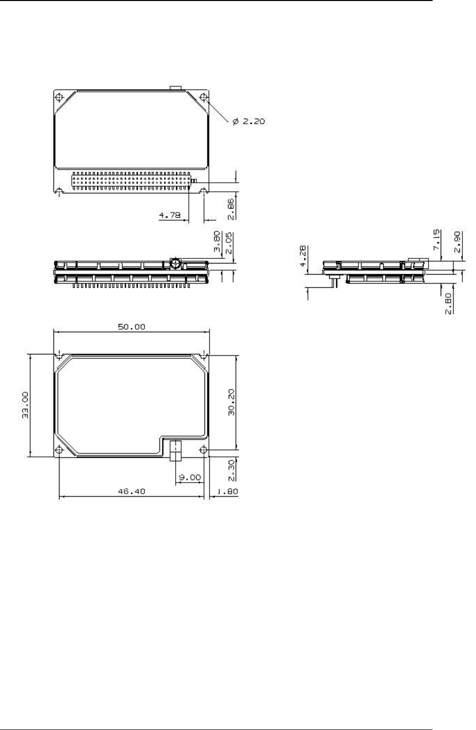
2.2 Physical Dimensions
Figure 2.2 Physical dimensions of GM 47/48
The measures are given in millimetre’s. See also chapter 6, Technical
Data.
GM47/48 Technical description
BA/SEM/MS 02:0004 Rev B
13
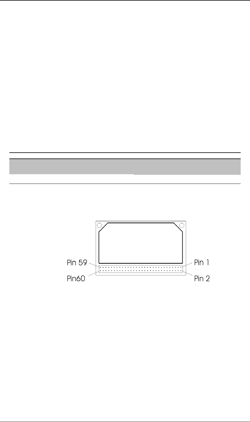
3 System Connector Interface
3.1 Overview
The electrical connections to the module (except the antenna), are set
through the System Connector Interface.
The connector shall allow the following connections: board to board
and board to cable. The table below provides the two possible mating
connectors for the application system:
No Pin Part Number Description
1 60 9462-9101-606 Female connector (Speed Tech). Board-
Board
2 60 TBD Female connector. Board-Cable
The figure 3.1 below indicates the pin numbering scheme.
Figure 3.1 GM 47/48. View from the underside
The table on next page provides the pin assignment of the different
signals in the System Connector Interface as well as a short
description of them.
All signal directions are with respect to the module i.e. Direction 'O'
means data being sent by the module.

GM47/48 Technical description
BA/SEM/MS 02:0004 Rev B
14
Pin Signal Name Dir Signal Type Description
1. VCC -Supply Power Supply
2. DGND - - Digital Ground
3. VCC -Supply Power Supply
4. DGND - - Digital Ground
5. VCC -Supply Power Supply
6. DGND - - Digital Ground
7. VCC -Supply Power Supply
8. DGND - - Digital Ground
9. VCC -Supply Power Supply
10. DGND - - Digital Ground
11. VCC -Supply Power Supply
12. DGND - - Digital Ground
13. Reserved for future use
14. ON/OFF IInternal pull up,
open drain Turns the module on/off
Former WAKE_B
15. SIMVCC -Dig. 3/5 V SIM card power supply
Power output for SIM Card from module
16. SIMPRESENCE IInternal pull up,
open drain SIM Presence
A "1" shall indicate that the SIM is missing;
a "0" that it is inserted.
17. SIMRST ODig. 3/5 V SIM card reset
18. SIMDATA I/O Dig. 3/5 V SIM card data
19. SIMCLK ODig. 3/5 V SIM card clock
20. DAC OAnalogue Digital to Analogue converter
21. IO1 I/O Digital, 2.75 General purpose input/output 1
22. IO2 I/O Digital, 2.75 General purpose input/output 2
23. IO3 I/O Digital, 2.75 General purpose input/output 3
24. IO4 I/O Digital, 2.75 General purpose input/output 4
25. VRTC ISupply 1.8 V Voltage for real time clock
26. ADC1 IAnalogue Analogue to Digital converter 1
27. ADC2 IAnalogue Analogue to Digital converter 2
28. ADC3 IAnalogue Analogue to Digital converter 3
29. SDA I/O 2.75, internal
pullup I2C Data
30. SCL O2.75, internal
pullup I2C Clock
31. BUZZER ODig. 2.75 Buzzer output from module
32. TIMESTAMP ODig. 2.75 Timestamp
Timestamp is reserved for future use, if A-
GPS is implemented on network side.

GM47/48 Technical description
BA/SEM/MS 02:0004 Rev B
15
33. LED ODig. 2.75 Flashing LED
34. VIO OPower Out 2.75 Module powered indication.
The VIO is a 2.75 V output that could
power external devices to transmit data
towards the GSM device to a 75mA max.
35. TX_ON ODig 2.75 This output shall indicate when the GSM
module is going to transmit the burst.
36. RI ODig. 2.75 Ring Indicator
37. DTR IDig. 2.75 Data Terminal Ready
38. DCD ODig. 2.75 Data Carrier Detect
39. RTS IDig. 2.75 Request To Send
40. CTS ODig. 2.75 Clear To Send
41. TD IDig. 2.75 Transmitted Data
Data from DTE (host) to DCE (module).
[former DTMS]
42. RD ODig. 2.75 Received Data
Data from DCE (module) to DTE (host).
[former DFMS]
43. TD3 IDig. 2.75 UART3 Transmission
Data from DTE (host) to DCE (module).
[former DTMS]
44. RD3 ODig. 2.75 UART3 Reception
Data from DTE (host) to DCE (module).
[former DTMS]
Data from DCE (module) to DTE (host).
[former DFMS]
45. TD2 IDig. 2.75 UART2 Reception
Former CTMS. Used for flashing
46. RD2 ODig. 2.75 UART2 Transmission
Data from DCE (module) to DTE (host).
[former DFMS]
Former CFMS. Used for flashing
47. PCMULD IDig. 2.75 DSP PCM digital audio input
48. PCMDLD ODig. 2.75 DSP PCM digital audio output
49. PCMO ODig. 2.75 Codec PCM digital audio output
50. PCMI IDig. 2.75 Codec PCM digital audio input
51. PCMSYNC ODig. 2.75 DSP PCM frame sync
52. PCMCLK ODig. 2.75 DSP PCM clock output
53. MICP IAnalogue Microphone input positive
54. MICN IAnalogue Microphone input negative
55. BEARP OAnalogue Speaker output positive
56. BEARN OAnalogue Speaker output negative
57. AFMS OAnalogue Audio output from module

GM47/48 Technical description
BA/SEM/MS 02:0004 Rev B
16
58. SERVICE I12V/2.7V Flash programming voltage for the MS.
Enable logger information if no flashing
Former VPPFLASH
59. ATMS IAnalogue Audio input to module
60. AGND - - Analogue ground
3.2 General Electrical and Logical Characteristics
Many of the signals present in the interface are high-speed CMOS
logic inputs or outputs powered from 2.75 V ± 5 %. Whenever a
signal is defined as Dig. 2.75 V, the following electrical
characteristics shall apply.
Parameter Min. Typ. Max. Output
current Io
Units
High Level Output Voltage (VOH)2.2 2.75 - 2 mA Volts
Low Level Output Voltage (VOL)00.6 2 mA Volts
High Level Input Voltage (VIH)1.93 2.75 Volts
Low Level Input voltage (VIL)00.5 Volts
3.2.1 General Protection Requirements
All 2.75V digital inputs shall continuously withstand any voltage from
-0.5V up to 3.47V (3.3V + 5%) in the power-on or power-off
condition with no damage. All 2.75V digital outputs shall
continuously withstand a short circuit to any voltage within the range
from 0V to 3V.
The SIM output signals and the SIMVCC supply shall continuously
withstand a short circuit to any voltage within the range from 0V to
4.1V.
3.3 Grounds
Pins Name Description
2, 4, 6, 8, 10, 12 DGND Digital Ground
60 AGND Analogue Ground

GM47/48 Technical description
BA/SEM/MS 02:0004 Rev B
17
There are two ground signals in GM 47/48, Analogue Ground
(AGND) and Digital Ground (DGND). The analogue Ground is
connected to pin number 60, and the Digital Ground is connected to
the System Connector Interface through pin numbers 2, 4, 6, 8, 10 and
12.
Note: All the Ground pins have to be connected to the application.
The AGND is connected to the DGND in the ME, and only there. It is
important that the AGND and the DGND are separated in the
application.
3.3.1 The Analogue Ground
The AGND lead is the analogue audio reference ground. It is the
return signal for Audio To Mobile Station (ATMS) and Audio From
Mobile Station (AFMS).
It shall be connected to the Digital Ground (DGND) inside the module
and only there. The application shall not connect DGND and AGND.
Parameter Limit
Imax ≅12.5mA
3.3.2 The Digital Ground (DGND)
DGND is the reference for all digital signals in the System Interface.
It shall also be the DC return for the power supply on VCC and
SERVICE. Each DGND pin is rated at 0.5 A. All DGND pins are
connected internally in the module.
Parameter Limit
Iaverage < 0.5 A No DGND pin can withstand over 0.5 A
Imax < 600 mA (100 mA each)
3.4 Regulated Power Supply
Pins Name Description
1, 3, 5, 7, 9, 11 VCC Regulated Power Supply
The regulated power supply, VCC, is connected to the pin numbers 1,
3, 5, 7, 9 and 11.

GM47/48 Technical description
BA/SEM/MS 02:0004 Rev B
18
3.4.1 Power Supply (VCC)
The VCC supplies the module with external power. Any other voltage
needed is generated internally.
Parameter Mode Limit
Voltage to be applied Nominal 3.6 Volts
Tolerance including ripple 23.4 Volts - 4.0 Volts
Over voltages 5.5 Volts
Current Drive capability at TX Full Power < 600 mA (average))
< 2 A (Peak)
GM 47/48 have not internal capacitance to supply the large current
peaks during GSM transmission. Therefore on burst transmission the
application DC source is responsible for providing the appropriate
current.
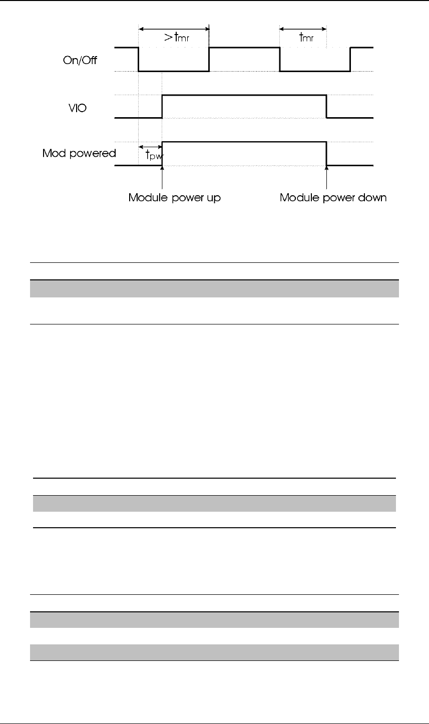
3.5 ON/OFF and External Power Signals
Pins Name Dir Description
14 ON/OFF ISquare signal to turn on/off the module
34 VIO OExternal power supply
3.5.1 Module ON/OFF
The module is powered ON/OFF by earthing (pulling low) pin 14 as
per figure 3.2 below. The pin should then be released as it is an
internal pull up to return it to the high state.
Note: Driving with 2.75V or 3.6V is not permitted and restrict module
functionality.
Parameter Minimum Typical Maximum Units
Voltage HIGH Level (FALSE) VCC By internal
pull up only
Voltage LOW Level (TRUE) 00.3*VCC Volts
Pull-up Resistance Internal pull up 39 KΩ
2Measured at system connector pins.
GM47/48 Technical description
BA/SEM/MS 02:0004 Rev B
19
Figure 3.2ON/OFF and VIO performance
Where the times are defined as follows:
Time Description Min Typ Max Unit
tMR Time to start an ON/OFF operation 11.5 S
tPWR Time for module start-up one ON/ OFF
signal has set to TRUE 100 200 Ms
3.5.2 External 2.75 V (VIO)
The VIO has been derived from a 2.75 V regulator. It is possible to
use this output as a power supply at 2.75 V with a maximum of 75mA.
It will indicate that the module is alive and it could power external
devices. In this case, the external applications do not need to
implement a 2.75 volt regulator to adapt the incoming (from module
point of view) serial data.
Parameter Minimum Typical Maximum Units
Output Voltage (Iload=50 mA) 2.70 2.75 2.85 Volts
Load current 75 mA
3.6 Analogue Audio
Pins Name Dir Description
57 AFMS OAudio From Mobile Station
59 ATMS IAudio To Mobile Station
60 AGND -Reference for analogue audio

GM47/48 Technical description
BA/SEM/MS 02:0004 Rev B
20
ATMS and AFMS are the audio input and output for the module. The
analogue audio signals can be used in two different modes, Normal
and Portable Handsfree.
Handsfree
This mode is referred to as Audio To Mobile Station (ATMS) and
Audio From Mobile Station (AFMS). It is used by audio accessories
such as Handsets and Handsfree equipment.
Portable Handsfree
This mode activates a different amplification factor in the Mobile
Equipment (ME). It also activates a microphone bias level in ATMS.
This is the default mode.
3.6.1 Audio To Mobile Station (ATMS)
ATMS is the analogue audio input to the module. It connects to the
audio input of the CODEC in the module. The CODEC then converts
the analogue audio to digital audio, in PCM format, which is
connected to the internal PCM bus in the module. The internal PCM
bus connects the encoded audio to PCMO on the system connector.
ATMS is also used as the microphone input from the Portable
Handsfree. If this is the case, a DC bias is provided from the ATMS.
All sources must be AC-coupled except the Portable HandsFree
microphone, which shall be DC-coupled in order to supply DC current
to the Portable HandsFree microphone. AC coupling prevents
incorrect biasing or damage of the ATMS input. The capacitor must
have a value greater than shown below to avoid attenuation of low
frequencies.
The ATMS input is a passive network followed by the transmit part of
the CODEC.
Parameter Limit
Application driving impedance (0.3 - 3.5 kHz) < 300 Ω
AC coupling capacitance
3> 1 µF
Module input impedance (0.3 - 3.5 kHz) >50ΚΩ
Low frequency cut-off (- 3 dB) 300 Hz ± 50 Hz
High frequency cut-off (- 3 dB) > 3500 Hz
Maximum allowed input level 1.5Vpp = 530mV
Output DC bias level Handsfree mode 0 V
3 AC coupling capacitance must be supplied by the application, unless a DC coupled microphone
is used.

GM47/48 Technical description
BA/SEM/MS 02:0004 Rev B
21
Portable Handsfree mode 2 V ± 0.1 V
Additional Gain in Portable Handsfree mode 28.5 dB
• Maximum input level at ATMS 245mVrms output at PCMO =
3dBm0
• The following table is with nominal PGA (Programmable Gain
Settings)
• For more information see AT commands
Input Input Volts mV
rms TXAGC dB AUXI1 Gain PCMO dBm0
ATMS 245 0 13 3
Maximum input level at MICI 61.4mVrms output at PCMO = 3dBm0
Input Input Volts mV
rms TXAGC dB AUXI1 Gain PCMO dBm0
MICI 61.4 0 25 3
Output at AUX02 for 3dBm0 at PCMI
Input dBm0 RXPGA Volume
Control dB AUX02 mV
rms
PCMI 3dBm0 0 0 436
Output at BEAR for 3dBm0 at PCMI
Input dBm0 RXPGA Volume
Control dB BEAR mV
rms
PCMI 3dBm0 0 0 388
GM47/48 Technical description
BA/SEM/MS 02:0004 Rev B
22
3.6.2 Audio From Mobile Station (AFMS)
AFMS is the analogue audio output from the module. When it is
active, the output is derived from the PCM digital audio by the
decoder part of the CODEC. The PCM data comes from PCMI on the
system connector. It is also used as an ear-piece driver for the Portable
Hands Free accessory.
Parameter Limit
Speaker impedance 64 Ω το 1ΚΩ
AFMS Output Capacitance 2.2 µF ±10%
Levels (THD < 5 %) Drive capability into 5 kΩ (0.3 -
3.5 kHz)
> 2.4 Vpp [TBC]
Drive capability into 1.5 kΩ (0.3 -
3.5 kHz) > 2.2 Vpp [TBC]
Drive capability into 150 Ω (at
1kHz)
> 1.3 Vpp [TBC]
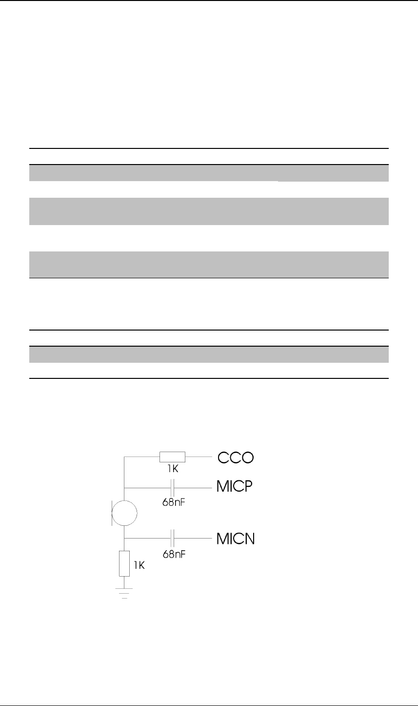
3.7 Microphone Signals
Pin Speaker signals Dir Function
53 MICP IMicrophone Positive Input
54 MICN IMicrophone Negative Input
MICP and MICN are the microphone-input pins. These inputs shall be
compatible with an electret microphone. The microphone contains a
FET buffer with open drain output, which must be supplied at least
+2V relative to ground.
Figure 3.3 Microphone connection to module
CCO is the source voltage that will provide the necessary drive
current for the microphone.
GM47/48 Technical description
BA/SEM/MS 02:0004 Rev B
23
Parameter Limit
CCO 2.0 - 2.5 V
3.8 Speaker Signals
Pin Speaker signals Dir Function
55 BEARP OMicrophone Positive Output
56 BEARN OMicrophone Negative Output
BEARP and BEARN are the speakers output pins. These outputs are
in differential mode.
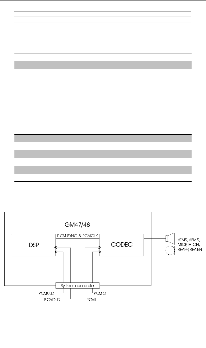
3.9 Digital Audio
Pin PCM signal Dir Function
52 PCMCLK OPCM clock
51 PCMSYNC OPCM frame sync
47 PCMULD IPCM audio input to DSP
48 PCMDLD OPCM audio output to DSP
50 PCMI IPCM audio input to Codec
49 PCMO OPCM audio output to Codec
The digital PCM audio signals allow the connection of a digital audio
source / receiver, bypassing the analogue audio CODEC processing
functions performed within the module.
Figure 3.4 Pin connections to digital audio

GM47/48 Technical description
BA/SEM/MS 02:0004 Rev B
24
In case no external audio processing is performed, then it is needed to
connect
PCMDLD and PCMI
PCMULD and PCMO
Electrical characteristics
The Dig. 2.75 V CMOS Output / Input electrical characteristics shall
apply, with DGND as the reference.
PCM interface format
The PCM format (for PCMULD and PCMDLD) shall follow a linear
PCM data I/O format of an industry standard Texas Instrument DSP.
It is the same format as the one used between the CODEC and the
DSP. The DSP is the source of the bit clock PCMCLK and the frame
synchronisation PCMSYNC. The data bits in PCMULD and
PCMDLD shall be aligned so that the MSB in each word occurs on
the same clock edge.
3.10 Serial Data
Pin Name Dir Description RS232 CCITT
Nº
41 TD ISerial data to module 103
42 RD OSerial data from module 104
39 RTS IRequest To Send 105
40 CTS OClear To Send 106
37 DTR IData Terminal Ready 108.2
38 DCD OData Carrier Detect 109
36 RI ORing Indicator 125
45 TD2 IUART 2 Data Transmission
46 RD2 OUART 2 Data Reception
43 TD3 OUART 3 Data Transmission
44 RD3 IUART 3 Data Reception

GM47/48 Technical description
BA/SEM/MS 02:0004 Rev B
25
The serial channels are used as asynchronous communication links
between an application system or accessory units connected to the
Module. They consist of three UART's. One of them, the first and
main one, shall have RS-232 functionality. The rest shall behave as
general- purpose serial data lines, except for special applications (such
as accessories for the UART2 and Bluetooth for UART 3).
The Dig. 2.75 V CMOS Output / Input electrical characteristics shall
apply, with DGND as the reference. Extra relevant data is specified
for some of the signals.
The only character format supported is 1 start bit, 8 bit data, non-
parity plus 1 stop bit, in total 10 bits per character.

GM47/48 Technical description
BA/SEM/MS 02:0004 Rev B
26
3.10.1 UART 1 (RS232) - RD, TD, RTS, CTS, DTR, DCD and RI
The UART1 signals form a 9 pin RS-232 (V.24) serial port, apart
from the DSR (CCITT Nº 107) signal. DSR signal has been removed
as it is usually connected to DTR in most systems.
The signal levels do not match the standard RS-232 (V.28) levels. The
relationship between the levels is shown in the table below
RS - 232 Level RD, TD RTS, CTS, DTR, DCD, RI 2.75 V CMOS Level
< - 3 V 1OFF > 1.93
> + 3 V 0ON < 0.80 V
Conversion between the 2.75V CMOS levels and the RS232 levels
can be achieved using a standard interface IC, such as the Maxim
Integrated Products MAX3237.
3.10.2 Serial Data Signals - RD, TD
The default baud rate is 9.6 kbit/s, however higher bit rates up to 460
kbit/s shall be supported, and set by an AT command. The UART 1
starts at a rate of 9.6 kbit/s in standard AT mode or binary mode (First
received data AT or binary will determine the operation mode).
The GSM 07.10 multiplexing protocol is supported and shall be
started on command. In this case bit rates up to 460 kbits/s shall be
supported.
Serial Data From Module (RD)
RD is an output used to send data on the UART 1 to the application
system. This is a Dig. 2.75 CMOS Output and general characteristics
are applicable.
Parameter Limit
Application load resistance < 100 kΩ
Application load capacitance < 500 pF
Serial Data To Module (TD)
TD is input (to the module) used by the application system to send
data on the UART 1 to the module. This is a Dig. 2.75 CMOS Input
and general characteristics are applicable.
Parameter Limit
Application driving impedance < 100 Ω
Input capacitance 1 nF
Input resistance (pull-up) 100 kΩ to 2.75 V

GM47/48 Technical description
BA/SEM/MS 02:0004 Rev B
27
3.10.3 Control Signals - RTS, CTS, DTR, DCD, RI
The control signals are active low, and hence when a standard
interface IC is used (such as MAX3237), then standard RS-232 levels
are obtained.
These signals together with DGND, RD and TD form a 9-pin RS-232
data port (with the exception of the voltage levels and DSR).
RTS and CTS shall be capable of transmitting at 1/10 of the data
transmission speed for data rates, up to 460 kbit/s. (Byte oriented flow
control mechanism).
Switching times for RTS and CTS
Parameter Limit
Time from Low to High level < 2 µs
Time from High to Low level < 2 µs
Request to Send (RTS)
RTS is an input to the module. The signals on this circuit shall be used
to condition the DCE (the module when used for data transmission
purposes) for data transmission. Default level is OFF, by internal pull
up.
The exact behaviour of RTS shall be defined by an AT command.
Software or hardware flow control can be selected. Hardware flow
control is the default.
This is a Dig. 2.75 CMOS Input and general characteristics are
applicable.
It is the duty of the application to pull RTS low (logic levels) to
request communications with the module. The module will respond by
asserting CTS low and as such may be used as a notification as a
module status ready for communication.
Parameter Limit
Application driving impedance < 100 Ω
Input capacitance < 2 nF
Input resistance (pull-down) 100 kΩ to DGND

GM47/48 Technical description
BA/SEM/MS 02:0004 Rev B
28
Clear To Send (CTS)
CTS is an output from the module. The signals on this circuit shall be
used to indicate that the DCE (the module when used for data
transmission purposes) is ready to transmit data. Default level is high.
The exact behaviour of CTS shall be defined by an AT command.
Software or hardware flow control can be selected.
This is a Dig. 2.75 CMOS Output and general characteristics are
applicable.
Tip: if only software flow control is to be used it becomes necessary
to assert RTS low or to connect RTS to CTS at the module.
Parameter Limit
Application load capacitance < 500 pF
Application load resistance > 1 MΩ
Data Terminal Ready (DTR)
DTR is an input to the module. Signals from the DTE on this circuit
indicate the DTE is ready to transmit and receive data. DTR also acts
as a hardware 'hang-up' so that calls are terminated if DTR is OFF
(high).
Default level is ON (low). The exact behaviour of DTR shall be
defined by AT commands.
This is a Dig. 2.75 CMOS Input and general characteristics are
applicable.
Data Carrier Detect (DCD)
DCD is an output from the module. An ON (low) signal shall indicate
that a valid carrier (data signal) is being received by the DCE
(module). The exact behaviour of DCD shall be defined by an AT
command.
This is a Dig. 2.75 CMOS Output and general characteristics are
applicable.
Ring Indicator (RI)
RI is an output from the module. An ON (low) signal shall indicate a
ringing signal is being received by the DCE (module).
The functionality shall be selected by an AT command.
This is a Dig. 2.75 CMOS Output and general characteristics are
applicable.

GM47/48 Technical description
BA/SEM/MS 02:0004 Rev B
29
Note: DSR is considered permanently ready for a module, therefore
any DGND connection may be taken as DSR functionality.
3.10.4 UART 2 - TD2, RD2
The UART 2 consists of a full duplex serial communication. This
involves the transmission and reception lines.
The communication port shall work in one mode: Operation and
Maintenance mode.
Operation and Maintenance mode shall work in addition with
SERVICE signal. On switching the module on, if SERVICE signal is
active then two events can happen. If no data is sent to the module,
then the logger is activated. Otherwise, the module shall be ready to
be reprogrammed.
Timing and Electrical signals characteristics equal to UART 1 TD and
RD, except for maximum baud rate that could be increased to 921
KBPS.
Transmitted Data 2 (TD2)
TD2 is input (to the module) used by the application system to send
data on the UART 2 to the module.
The electrical characteristics shall be the same as TD.
Received Data 2 (RD2)
RD2 is an output used to send data on the UART 2 to the application
system.
The electrical characteristics shall be the same as RD.
3.10.5 UART 3 - TD3, RD3
The UART 3 consists of a full duplex serial communication. This
involves the transmission and reception lines.
Timing and electrical signals characteristics equal to UART 1 TD and
RD.
Transmitted Data 3 (TD3)
TD3 is input (to the module) used by the application system to send
data on the UART 3 to the module.
The electrical characteristics shall be the same as TD.

GM47/48 Technical description
BA/SEM/MS 02:0004 Rev B
30
Received Data 3 (RD3)
RD is an output used to send data on the UART 3 to the application
system.
The electrical characteristics shall be the same as RD.
3.11 SIM Card related signals
Parameter Mode Signal Min. Typ. Max. Unit
SIM supply Voltage 3 V SIMVCC 2.7 3.0 3.3 V
5 V 4.5 5.0 5.5 V
High Level Input Voltage
(VIH)3 V SIMDAT 2.1 3.0 V
5 V 3.5 5.0 V
Low Level Input Voltage
(VIL)3 V SIMDAT 00.9 V
5 V 01.5 V
High Level Output Voltage
(VOH)3 V SIMDAT 2.7 3.0 V
5 V 4.7 5.0 V
Low Level Output Voltage
(VOL)3 V SIMDAT 00.2 V
5 V 00.2 V
High Level Output Voltage
(VOH)3 V SIMCLK
SIMRST
2.4 3.0 V
5 V 4.4 5.0 V
Low Level Output Voltage
(VOL)3 V SIMCLK
SIMRST
00.35 V
5 V 00.3 V

GM47/48 Technical description
BA/SEM/MS 02:0004 Rev B
31
3.11.1 SIM Detection – SIM Presence
SIMDETECT is an input intended to be used to determine whether a
SIM card has been inserted or removed in the external SIM card
holder. It shall be normally wired to the "Card Inserted Switch" of the
external SIM card holder, but different implementation could be
handled.
On having High level it will mean, "SIM card missing". While pulled
down to Low the module shall understand it as "SIM card inserted".
SIMDETECT is Dig. 2.75 CMOS input and general characteristics are
applicable.
Parameter Min. Typ. Max. Units
Pull-up resistance (at 2.75 V) 100 kΩ
Low Level Input Voltage (SIM inserted) 0.8 V
High Level Input Voltage (SIM missing) 1.93 5V
3.12 Service/Programming
Pin Signal Description
58 SERVICE Flash programming voltage
This input shall be used as a programming voltage for the Flash
Memories to initiate and speed up the programming process, or a
signal to indicate the module a logging process.
Mode
SERVICE Voltage (V)
Drive Capacity
Mode SERVICE Voltage (V) Drive Capacity
Min. Typ. Max.
Normal Operation 0.8 -
Service/enable programming 1.9 2.75 3.6 > 1 mA
Fast programming 11.4 12.6 > 60 mA
Absolute maximum voltage 13.5 -
The maximum accumulated time allowed with Programming voltage
applied shall be 80 h. over the lifetime of the module.
GM47/48 Technical description
BA/SEM/MS 02:0004 Rev B
32
3.13 Buzzer
Pin Signal Description
31 BUZZER Buzzer Output from module
This is an output signal which allows the application to use pre-
programmed melodies or sounds. Typical use would involve a
transistor buffer with a piezoelectric sounder.
The Dig. 2.75 V CMOS Output electrical characteristics shall apply,
with DGND as the reference.
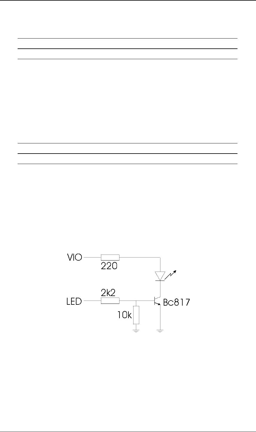
3.14 LED
Pin Signal Description
33 LED LED Output from module
This is an output signal which allows the use of an external LED. The
LED shall indicate different states within the module.
This signal is a Dig. 2.75 V CMOS output so general characteristics
are applicable. In order to connect a LED in the external application
following scheme shall be followed.
The operation of the LED is hardcoded and is not controlled by the
host application.
Figure 3.5 Electrical connection for led

GM47/48 Technical description
BA/SEM/MS 02:0004 Rev B
33
3.15 TX_ON - Burst Transmission
Pin Signal Dir Description
35 TX_ON OGSM module on transmission
The TX_ON is a digital signal output. This shall indicate that the
module is going to transmit the burst. Burst transmission is the time
when a GSM transceiver unit.
Dig 2.75 CMOS Output so general electrical characteristics are
applicable.
3.16 Timestamp
Pin Signal Dir Description
32 TIMESTAMP OGlobal Positioning System Timestamp
TIMESTAMP is a Dig. 2.75 V CMOS Output electrical
characteristics, with DGND as the reference.
Its main purpose is the A-GPS timestamp. As it is shown this is only
applicable when the Assisted GPS is implemented. In order to apply
the assisted GPS performance not only MS implementation is
necessary but network side as well.
GM47/48 Technical description
BA/SEM/MS 02:0004 Rev B
34
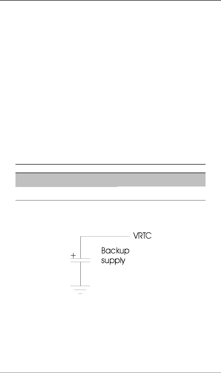
3.17 Real Time Clock
The Real Time Clock provides with a time-of-day calendar with alarm
and one hundred-year calendar to the main microprocessor.
The real time clock operates with a separate power supply. Therefore,
two modes of operation shall be distinguished:
RTC Normal operation: This is when the MS is powered, and it does
not take into account if the MS is in OFF, ON or SLEEP mode.
RTC Backup operation: This operation is performed when the MS is
not powered, VCC = 0V. In this case the RTC operation is maintained
by the backup power supply.
The backup power supply is a passive power supply, capacitor,
golden- capacitor, battery etc., which shall be connected outside the
MS to VRTC pin. During the RTC normal operation, the passive
power supply is being charged; this is like charging a capacitor.
In backup operation, the backup source provides with enough voltage
for RTC operations. Following table shows both voltage operations
characteristics.
Parameter Min. Typ. Max. Units
Supply Voltage RTC (Normal Operation –
Charging the capacitance) 1.6 1.8 2.0 V
Supply Voltage RTC (Backup Operation –
Capacitance provides with voltage) 1.0 1.8 2.0 V
In Back-up operation if the voltage drop below 1.0 Volts, the RTC
shall stop working. Following picture shows the RTC connection:
Figure 3.6 RTC connection
A typical value for this capacitor will be 0.16F, this will power the
RTC for approximately 6 hours.

GM47/48 Technical description
BA/SEM/MS 02:0004 Rev B
35
4 Antenna Connector
The Antenna Connector is a hub for transmission of the Radio
Frequency (RF) signals from the module to the external customer-
supplied antenna. It is a microminiature coaxial MMCX connector
that is mounted on the surface of the module. One provider of
Antenna Connectors is IMS.
This table provides the electrical characteristics at the antenna
interface.
Parameter Limit Description
Nominal impedance 50 Ω (SWR < 2:1)
Output Power 2 Watt peak (Class 4) Extended GSM 900
1 Watt peak (Class 1) GSM 1800
Static Sensitivity Better than - 102 dBm Extended GSM 900
Better than - 102 dBm GSM 1800

GM47/48 Technical description
BA/SEM/MS 02:0004 Rev B
36
5 AT Command Summary
The AT standard is a line-oriented command language. "AT" is an
abbreviation of ATtention and it is always used to start sending a
command line from a TE to the TA. TE stands for Terminal
Equipment which is a computer of any size and TA stands for
Terminal Adapter which is the modem part of the module.
The command line consists of a string of alphanumeric characters. It is
sent to the modem to instruct it to perform the commands specified by
the characters.
Functionality AT commands
CONTROL AND IDENTIFICATION
Subscriber Information AT+CNUM, AT+CIMI, AT*ESNU
Product & Release info AT+CGMI, AT+CGMM, AT+CGMR,
AT+CGSN, AT*ESIR
Generic information & Settings AT, AT*, AT+CLAC, AT+GCAP, ATI,
AT+CSCS, AT&F, AT&W, ATZ, AT+WS46
CALL CONTROL ATA, ATD, ATL, ATH, ATO, ATP, ATT,
AT+CHUP, AT+CMOD, AT+VTS, AT+CVHU,
AT+CR, AT+CRC, AT+CRLP
AUDIO CONTROL AT*EALR, AT*EAMS, AT*EARS, AT*ELAM,
AT*EMIR, AT*EMIC, AT*EXVC
NETWORK SERVICES
Alternate Line Service (ALS) AT*EALS, AT*ELIN, AT*ESLN
Customer Service Profile AT*ECSP
Call forwarding AT+CCFC, AT*EDIF, AT*EDIS
Calling/called number identification AT+CLIP, AT+CLIR, AT*EIPS
Preferred networks AT*EPNR, AT*EPNW
Advice of Charge AT+CACM, AT+CAMM, AT+CAOC,
AT+CPUC
Calling cards AT*ESCN
Call hold, waiting & multiparty AT+CCWA, AT+CHLD
Operator selection AT+COPS
Network registration AT+CREG
USSD AT+CUSD, AT+ CSSN
Security & Locks AT+CLCK, AT+ CPWD, AT+CPIN, AT*EPEE
SETTINGS AT*EMAR, AT*ERIL, AT*ERIN, AT*ERIP,
AT*ESIL, AT*ESMA, AT*ESMM, AT*ESOM,

GM47/48 Technical description
BA/SEM/MS 02:0004 Rev B
37
AT*ECPI
ME STATUS INFORMATION AT*ECAM, AT+CSQ, AT+CBC, AT+CIND,
AT+CPAS, AT+CMER
ERROR CONTROL AT+CMEE, AT+CEER
SMS & CB
Settings AT*ESTL, AT+CPMS, AT+CRES, AT+CSAS,
AT+CSCA, AT+CSMS, AT+CNMI, AT+CSDH,
AT+CSMP, AT+CGSMS
SMS-Command AT+CMGC
Read / write SMS AT+CMGD, AT+CMGW, AT+CMGL,
AT+CMGR
Send SMS AT+CMGS, AT+CMSS
PHONEBOOK
Read / write / find AT+CPBS, AT+CPBR, AT+CPBW, AT+CPBF
Call screening AT*ECAR, AT*ECAS, AT*ECAW
Groups AT*EGIR, AT*ESAC, AT*ESCG, AT*ESDG,
AT*ESDI, AT*ESGR
Personal Rings AT*EPRR, AT*EPRW
Settings AT*EPBM, AT*ESIA, AT*E2PCS
CLOCK
Alarm AT+CALA, AT+CALD, AT+CAPD
Time & Date AT+CCLK, AT+CTZU, AT*EDST
WAP
Bookmarks AT*EWBA, AT*EWBR
Settings AT*EWCG, AT*EWCT, AT*EWDT,
AT*EWHP, AT*EWIL, AT*EWLI, AT*EWPB,
AT*ENAD, AT*EWSA, AT*EWSG
Profiles AT*EWPN, AT*EWPR
INTERFACE COMMANDS AT&C, AT&D, AT+ICF, AT+IFC, AT+ILRR,
AT+IPR, ATE, AETM, ATQ, ATS0, ATS10,
ATS2, ATS3, ATS4, ATS5, ATS6, ATS7,
ATS8, ATV, ATX, AT+CSCS
DATA COMPRESSION V42bis AT+DR, AT+DS
07.10 MULTIPLEXING AT+CMUX

GM47/48 Technical description
BA/SEM/MS 02:0004 Rev B
38
HSCSD AT+CHSR, AT+CHSU
GPRS
PDP Context Activation AT+CGACT
Manual PDP Context Activation AT+CGANS
GPRS Attachment AT+CGATT
Enter Data State AT+CGDATA
Define PDP Context AT+CGDCONT
GPRS Event Reporting AT+CGEREP
Show PDP Address AT+CGPADDR
Quality of Service Profile (MINIMUM
ACCEPTABLE) AT+CGQMIN
Quality of Service Profile (REQUESTED) AT+CGQREQ
GPRS Network registration Status AT+CGREG
Extension of ATD for GPRS ATD*
NETWORK INFORMATION
Cell information AT*E2CD
Engineering Mode AT*E2EMM
SIM APPLICATION TOOLKIT
Set Up Call AT*E2STKC
Display Text AT*E2STKD
Get Inkey AT*E2STKG
Get Input AT*E2STKI
Select Item AT*E2STKL
Set Up Menu AT*E2STKM
Envelope (Menu Selection) AT*E2STKN
Application Toolkit Settings AT*E2STKS

GM47/48 Technical description
BA/SEM/MS 02:0004 Rev B
39
6 Technical Data
Mechanical specifications
Maximum length: 50 mm
Maximum width: 33 mm
Maximum thickness: 6.82 mm (without system connector pins length)
Weight: 18,5 g
Power supply voltage, normal operation
Voltage: 3.6V Nominal
Tolerance ±0.2V
Ripple: <100mV @ 200KHz, <20mV @>200KHz
Voltage must always stay within a normal operating range, ripple included.
Power consumption: Speech mode < 600 mA (< 2 A peak)
Idle mode: 20 mA
Switched off: < 100 µA
Radio specifications
Frequency range: GM 47: EGSM 900 MHz and 1800 MHz (Dual Band)
GM 48: GSM 850 MHz and 1900 MHz (Dual Band)
Maximum RF output power: 2 W / 1 W
Antenna impedance: 50 Ω
SIM card
SIM card interface: 3 V or 5 V
Support of external SIM card
Environmental specifications
Operating temperature range: -25 0C to +55 0C
Storage temperature range: -40 0C to +85 0C
Maximum relative humidity: 95% at +40 0C
Stationary vibration, sinusoidal: Displacement: 7.5 mm Acceleration amplitude: 20 m/s 2 40
m/s 2 Frequency range: 2-8 Hz 8-200 Hz 200-500 Hz
Stationary vibration, random Acceleration spectral density (m2/s2): 0.96 2.88 0.96
Frequency range: 5-10 10-200 200-500 60 min per/axis
Non-stationary vibration, including
shock Shock response spectrum I, peak acceleration: - 3 shocks in
each axis and direction: 300 m/s 2, 11 ms

GM47/48 Technical description
BA/SEM/MS 02:0004 Rev B
40
Shock response spectrum II, peak acceleration: - 3 shocks in
each axis and direction: 1000 m/s2, 6 ms
Bump: Acceleration 250 m/s 2
Free fall transportation: 1.2 m
Rolling pitching transportation: Angle: ±35 degrees, period: 8s
Static load: 10 kPa
Low air pressure/high air pressure: 70 kPa / 106 kPa
Storage
SMS Storage capacity 40 in ME
In addition the unit can handle as many SMS as the SIM can
store (SIM dependent).
Phone book capacity 100
DAC
Parameter Value Units
Resolution 8bit
Output voltage swing for Code=00HEX 0.138 ± 0.1 V
Output voltage swing for Code=FFHEX 2.61 ± 0.2 V
Nominal Step Size 9.668 ± 0.1 mV
Linear Code Range 8-247 (8H-F7H)LSB
Absolute Error during Linear Range ±100 mV
Conversion Speed <100 µs
ADC
Parameter Value Units
Resolution 8bit
Input voltage for Code=00H0.01 ± 0.01 V
Input voltage for Code=FFH2.75 ± 0.1 V
Nominal Step Size 10.742 mV
Accuracy ±3LSB
Input Impedance >1 MΩ
Conversion Time to within 0.5bit <100 µs