Sysgration SY-SHE-M-001 BLE Mesh Module User Manual CSR1012 BLE Module PRD ForFCC V0 5 20150903
Sysgration Ltd. BLE Mesh Module CSR1012 BLE Module PRD ForFCC V0 5 20150903
Users Manual
SYSGRATION / Avi-on Confidential & Proprietary
2015-09-03
5
Product Features
CSR 1012 Single Chip solution:
Bluetooth Specification 4.1 compliant
128KB memory: 64KB RAM and 64KB ROM
RF Features:
Transmitter Power: ≧0 dBm
Receiver sensitivity: -85 dBm Typ
External EEPROM memory provides storage for the Bluetooth software parameter and
application parameter
Electrical:
DC Supply: 1.8V ~3.6V
Low current consumption: 16 mA @3V (Peak Current)
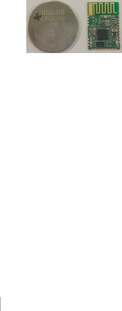
Small size: 18mm × 12mm ×2.3mm (L x W x H)
SYSGRATION / Avi-on Confidential & Proprietary
2015-09-03
5
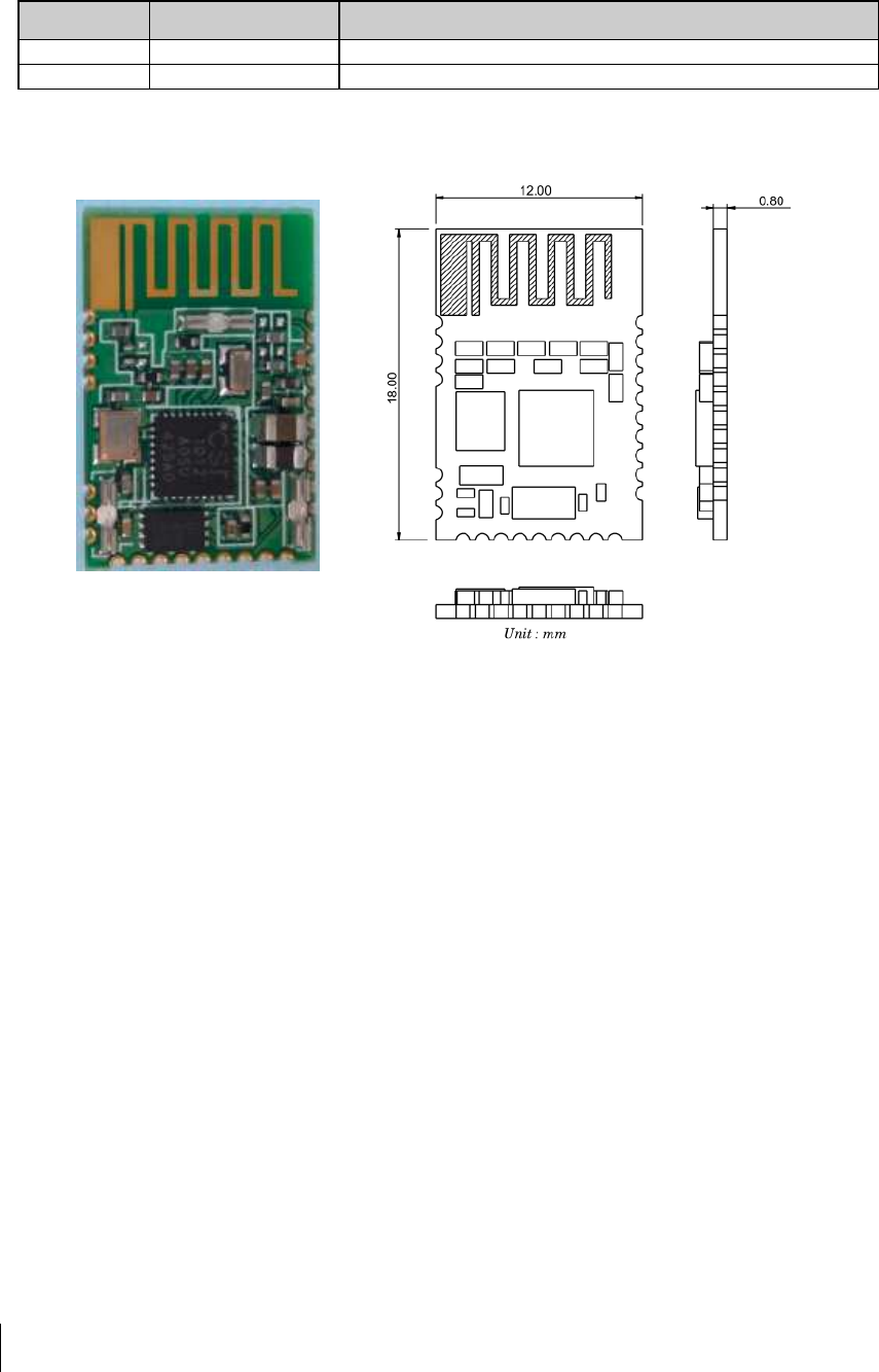
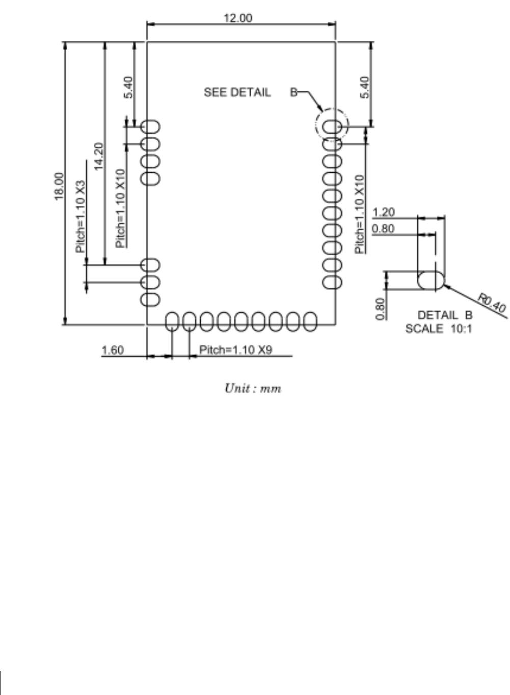
2.6 Mechanical Requirements
Item Feature Detailed Description
2.6.1 PCB 12 mm * 18 mm * 0.8mm
2.6.2 Weight N/A
Top View:
SYSGRATION /Avi-on Confidential & Proprietary
2015-09-03
5
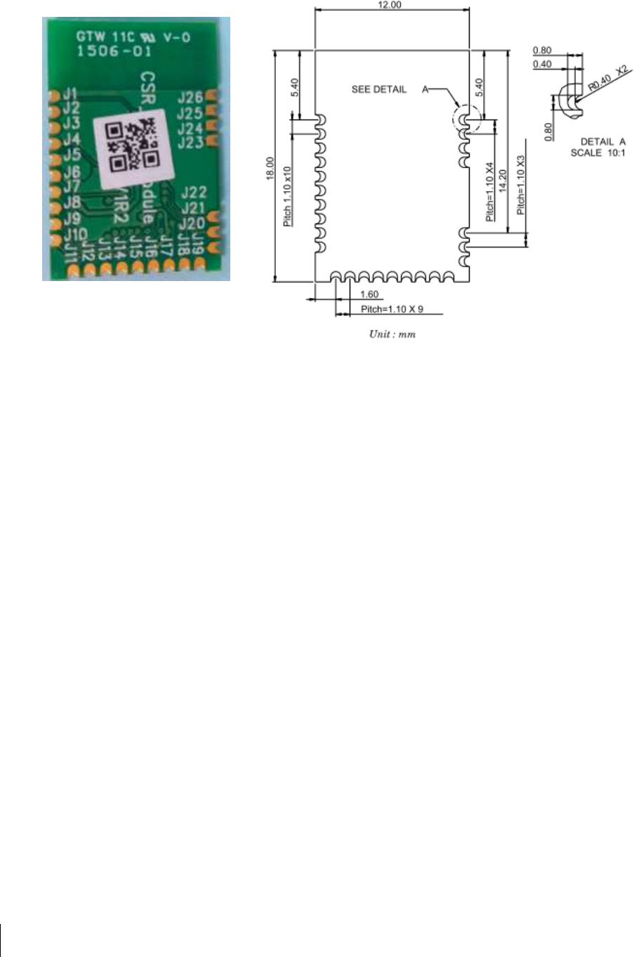
Bottom View:
SYSGRATION / Avi-on Confidential & Proprietary
2015-09-03
5
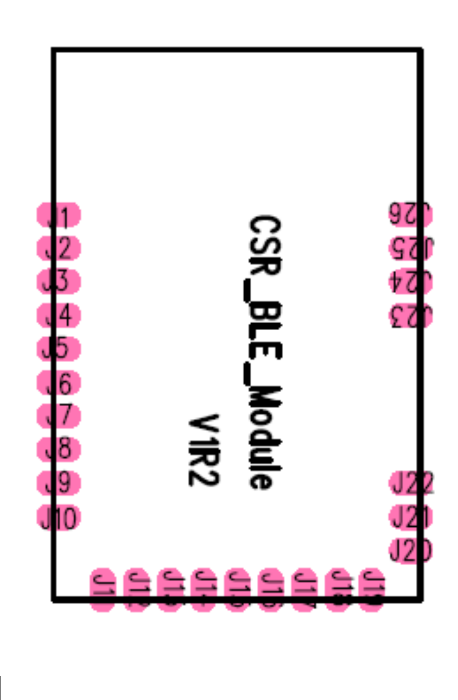
2.7 Pin Assignment:

SYSGRATION /Avi-on Confidential & Proprietary
2015-09-03
5
Pin Assignment Description:
Pins
Name Function
Description
J1 WAKE I Input to wake CSR1012 from hibernate or
dormant. Default is pull-down.
J2 XTAL_32K_IN Analog in
32.768KHz installed, Disconnect all to this Pin.
J3 XTAL_32K_OUT Analog In
32.768KHz installed, Disconnect all to this Pin.
J4 I2C_SCL I/O SPI serial flash installed, or I2C clock Input /
output.
J5 VBATT Power Power input.
J6 I2C_SDA I/O SPI serial flash installed, or I2C data Input /
output.
J7 SPI_PION I Selects SPI debug or Programmable I/O,
Pull-High : SPI debug
Pull-down: Programmable I/O line, default is.
J8 PIO[11] I/O Programmable I/O
J9 PIO[10] I/O Programmable I/O
J10 PIO[9] I/O Programmable I/O
J11 SPI_MISO O SPI data output or Programmable I/O
J12 SPI_MOSI I SPI data input or Programmable I/O
J13 SPI_CSB I SPI select or Programmable I/O
J14 SPI_CLK I/O SPI clock or Programmable I/O
J15 PIO[4] I/O Programmable I/O
J16 VDD_PADS Power Positive supply for all digital I/O ports
J17 PIO[3] I/O Programmable I/O
J18 UART0_RX I UART RX or Programmable I/O
J19 UART0_TX O UART TX or Programmable I/O
J20 AIO[0] I/O Analogue Programmable I/O
J21 AIO[1] I/O Analogue Programmable I/O
J22 AIO[2] I/O Analogue Programmable I/O
J23 GND Ground Ground
J24 GND Ground Ground
J25 GND Ground Ground
J26 GND Ground Ground
SYSGRATION / Avi-on Confidential & Proprietary
2015-09-03
5
Recommended of PCB Layout Pads
Federal Communication Commission Interference Statement
This equipment has been tested and found to comply with the limits for a Class
B digital device, pursuant to Part 15 of the FCC Rules. These limits are
designed to provide reasonable protection against harmful interference in a
residential installation.
This equipment generates, uses and can radiate radio frequency energy and, if
not installed and used in accordance with the instructions, may cause harmful
interference to radio communications. However, there is no guarantee that
interference will not occur in a particular installation. If this equipment does
cause harmful interference to radio or television reception, which can be
determined by turning the equipment off and on, the user is encouraged to try
to correct the interference by one of the following measures:
. Reorient or relocate the receiving antenna.
. Increase the separation between the equipment and receiver.
. Connect the equipment into an outlet on a circuit different from that to which
the receiver is connected.
. Consult the dealer or an experienced radio/TV technician for help.
FCC Caution: To assure continued compliance, any changes or modifications
not expressly approved by the party responsible for compliance could void the
user's authority to operate this equipment. (Example - use only shielded
interface cables when connecting to computer or peripheral devices).
End Product Labeling
This transmitter module is authorized only for use in devices where the
antenna may be installed such that 0.5 cm may be maintained between the
antenna and users. The final end product must be labeled in visible area with
the following: “Contains FCC ID: HQXSY-SHE-M-001”
”
End Product Manual Information
The user manual for end users must include the following information in a
prominent location “IMPORTANT NOTE: To comply with FCC RF exposure
compliance requirements, the antenna used for this transmitter must be
installed to provide a separation distance of at least 0.5 cm from all persons
and must not be colocated or operating in conjunction with any other antenna
or transmitter.” This device complies with part 15 of the FCC rules. Operation
is subject to the following two conditions (1) This device may not cause harmful
interference and (2) This device must accept any interference received,
including interference that may cause undesired operation.
IMPORTANT NOTE: In the event that these conditions can not be met (for
example certain laptop configurations or colocation with another transmitter),
then the FCC authorization is no longer considered valid and the FCC ID can
not be used on the final product. In these circumstances, the OEM integrator
will be responsible for reevaluating the end product (including the transmitter)
and obtaining a separate FCC authorization. This device is intended only for
OEM integrators under the following conditions: The antenna must be installed
such that 0.5 cm is maintained between the antenna and users. As long as a
condition above is met, further transmitter test will not be required. However,
the OEM integrator is still responsible for testing their end product for any
additional compliance requirements required with this module installed (for
example, digital device emissions, PC peripheral requirements, etc.).