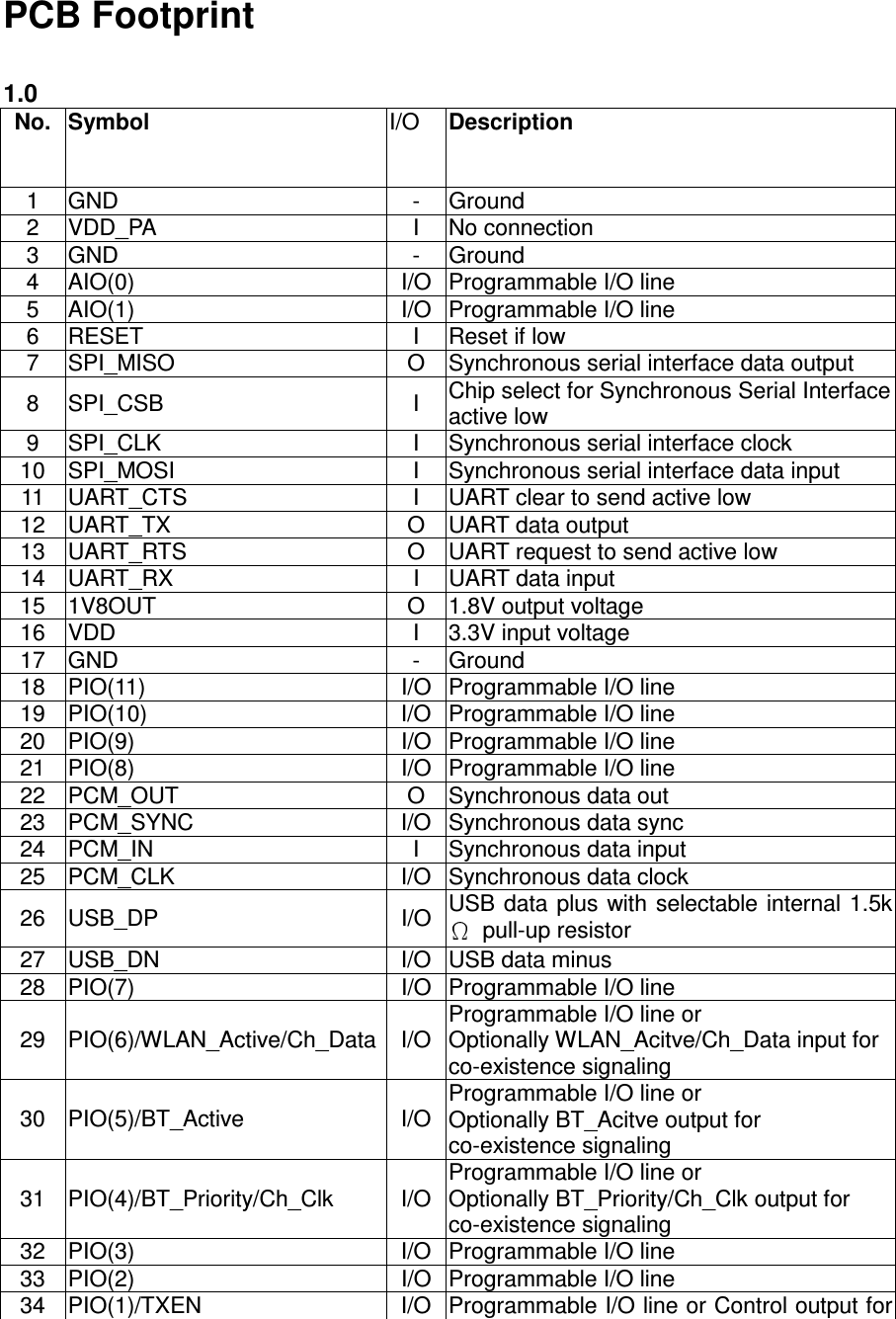
TAIDOC TECHNOLOGY H4000BEM2 Bluetooth Module User Manual Manual

TAIDOC TECHNOLOGY CORP. Bluetooth Module Manual

Manual

               Manual   Version 1.1             Product:    BC4 Module   Model No. :  H4000   Date:    June 12, 2009
H4000 Bluetooth Module   KEY FEATURES Support SPP, HID, HSP,A2DP,AVRCP, BIP Profile.. Bluetooth 2.0+EDR Power Level Class 2 (<4dBm) High sensitivity -85dBm Printing Antenna   APPLICATIONS PDA and smart phone. Digital frame with Bluetooth file transfer supporting. GPS receiver. Botebook PC and UMPC.   Picture       TOP VIEW PHYSICAL SIZE 32mm X 14.5mm X 1.92mm
CONTENTS 1. Key fecture..………………………………………………………………………2 2. Applictions………………………………………………………………………...2 3. Picture…………………………………………..…………………………………..2 4. Dimension…………………………………….…………………………………….4 5. PCB footpoint……………………………….………..………………………...5 6. Diagram……………………………………..………………………………………7 7. Bundled Software……………………….………….………………………….7 8. Electrical Characteristics…………………………………………………..8 9. Contact Information…..…………………………………………………..10 10. Document History………………………………………………………….11
Hardware Pad Functions   Dimension   36GNDGNDVDD_PAAIO0AIO1RESETSPI_MISOSPI_CSBSPI_MOSISPI_CLKUART_CTSUART_TXUART_RTSUART_RX1V8OUTVDDGNDGNDPIO0PIO1PIO2PIO3PIO4PIO6PIO5PIO7USB_D-USB_D+PCM_CLKPCM_INPCM_SYNCPCM_OUTH4000TOPVIEW1PIO11PIO10PIO8PIO914.5mm32mm1.279.827.281.86
PCB Footprint  1.0  No. Symbol  I/O  Description 1  GND  -  Ground 2  VDD_PA  I  No connection 3  GND  -  Ground 4  AIO(0)  I/O Programmable I/O line 5  AIO(1)  I/O Programmable I/O line 6  RESET  I  Reset if low 7  SPI_MISO  O  Synchronous serial interface data output 8  SPI_CSB  I  Chip select for Synchronous Serial Interface active low 9  SPI_CLK  I  Synchronous serial interface clock 10  SPI_MOSI  I  Synchronous serial interface data input 11  UART_CTS  I  UART clear to send active low 12  UART_TX  O  UART data output 13  UART_RTS  O  UART request to send active low 14  UART_RX  I  UART data input 15  1V8OUT  O  1.8V output voltage 16  VDD  I  3.3V input voltage 17  GND  -  Ground 18  PIO(11)  I/O Programmable I/O line 19  PIO(10)  I/O Programmable I/O line 20  PIO(9)  I/O Programmable I/O line 21  PIO(8)  I/O Programmable I/O line 22  PCM_OUT  O  Synchronous data out 23  PCM_SYNC  I/O Synchronous data sync 24  PCM_IN  I  Synchronous data input 25  PCM_CLK  I/O Synchronous data clock 26  USB_DP  I/O USB data plus with selectable internal 1.5k  pull-up resistor 27  USB_DN  I/O USB data minus 28  PIO(7)  I/O Programmable I/O line 29  PIO(6)/WLAN_Active/Ch_Data I/O Programmable I/O line or Optionally WLAN_Acitve/Ch_Data input for co-existence signaling 30  PIO(5)/BT_Active  I/O Programmable I/O line or Optionally BT_Acitve output for co-existence signaling 31  PIO(4)/BT_Priority/Ch_Clk  I/O Programmable I/O line or Optionally BT_Priority/Ch_Clk output for co-existence signaling 32  PIO(3)    I/O Programmable I/O line 33  PIO(2)  I/O Programmable I/O line 34  PIO(1)/TXEN  I/O Programmable I/O line or Control output for
external PA (if fitted) 35  PIO(0)/RXEN  I/O Programmable I/O line or Control output for external LNA (if fitted)   36  GND  -  Ground
Hardware Block Diagram   Main chipCSR BC417Flash 8M bitCrystal16MHzBalunFrequency range : 2.400GHz ~ 2.480GHz      Bundled Software  Bluepacket FW 43.TDR11.403, support SPP-B profile .
Electrical Characteristics       Absolute Maximum Ratings Rating  Min  Max Storage temperature  -40 oC  +90 oC Supply Voltage  -0.4V  3.7V  Recommended Operating Conditions Operating Condition  Min  Max Operating temperature range  -0oC  +70 oC Guaranteed RF performance range  -40 oC  +105 oC Supply voltage  3.0V  3.6V
RF Transmitter       RF Receiver
      Contact Information Bluepacket Communications Co., Ltd.   5F.-2,No.12,Lane 270,Sec.3,Beishen Rd.,Shenkeng Township,Taipei County 222, Taiwan (R.O.C ) TEL 886-2-26649168 FAX 886-2-26649166
Document History    Date  Revision  Reason of change November 22, 2005  V1.0  Original publication June 12, 2009  V1.1  Modify
Federal Communications Commission (FCC) Statement   15.21 You are cautioned that changes or modifications not expressly approved by the part responsible for compliance could void the user’s authority to operate the equipment.   15.105(b) This equipment has been tested and found to comply with the limits for a Class B digital device, pursuant to part 15 of the FCC rules. These limits are designed to provide reasonable protection against harmful interference in a residential installation. This equipment generates, uses and can radiate radio frequency energy and, if not installed and used in accordance with the instructions, may cause harmful interference to radio communications. However, there is no guarantee that interference will not occur in a particular installation. If this equipment does cause harmful interference to radio or television reception, which can be determined by turning the equipment off and on, the user is encouraged to try to correct the interference by one or more of the following measures:  -Reorient or relocate the receiving antenna. -Increase the separation between the equipment and receiver. -Connect the equipment into an outlet on a circuit different from that to which the receiver is connected. -Consult the dealer or an experienced radio/TV technician for help.  This device complies with Part 15 of the FCC Rules. Operation is subject to the following two conditions: 1) this device may not cause harmful interference, and 2) this device must accept any interference received, including interference that may cause undesired operation of the device.
FCC RF Radiation Exposure Statement:  This equipment complies with FCC radiation exposure limits set forth for an uncontrolled environment. End users must follow the specific operating instructions for satisfying RF exposure compliance. This transmitter must not be co-located or operating in conjunction with any other antenna or transmitter. Note: The end product shall has the words  “Contains Transmitter Module FCC ID: _________________________  TM7H4000BEM2

Navigation menu