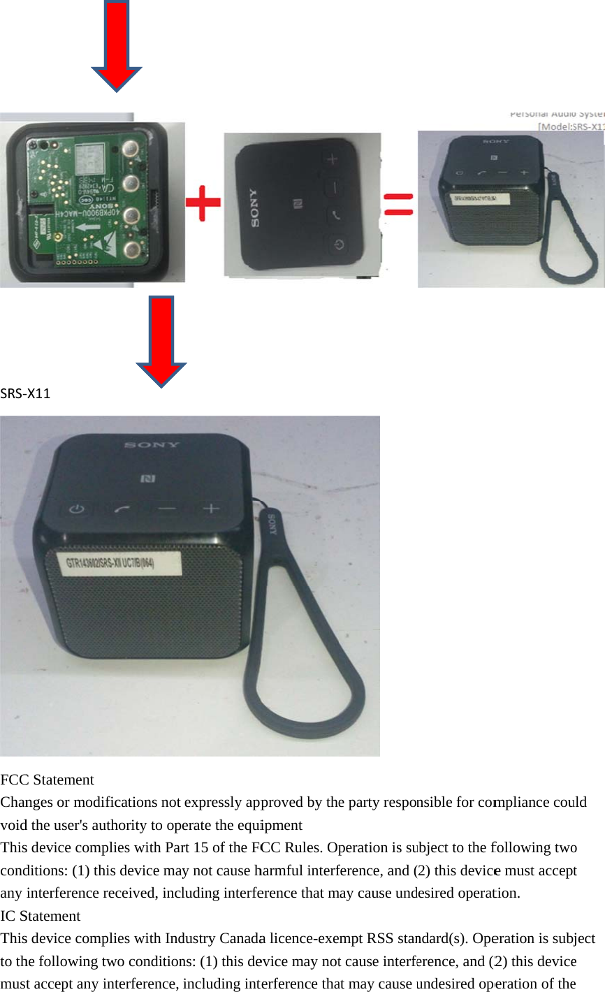
TCL Technoly Electronics 07 Bluetooth Module User Manual BM90SPKA5MG7 101x
TCL Technoly Electronics (Huizhou) Co., Ltd. Bluetooth Module BM90SPKA5MG7 101x
UserManual.wiki
>
TCL Technoly Electronics
>
07 User Manual
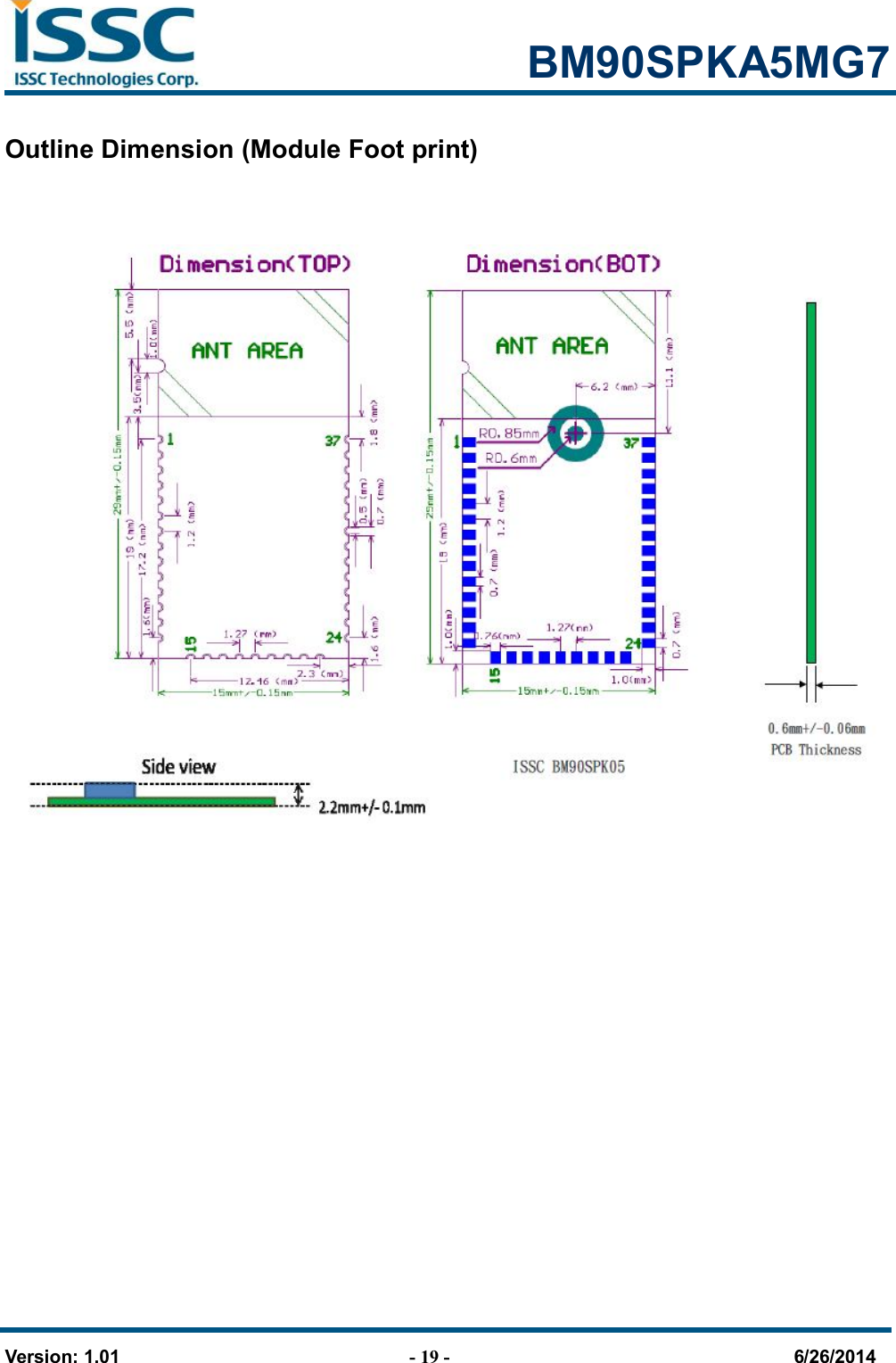
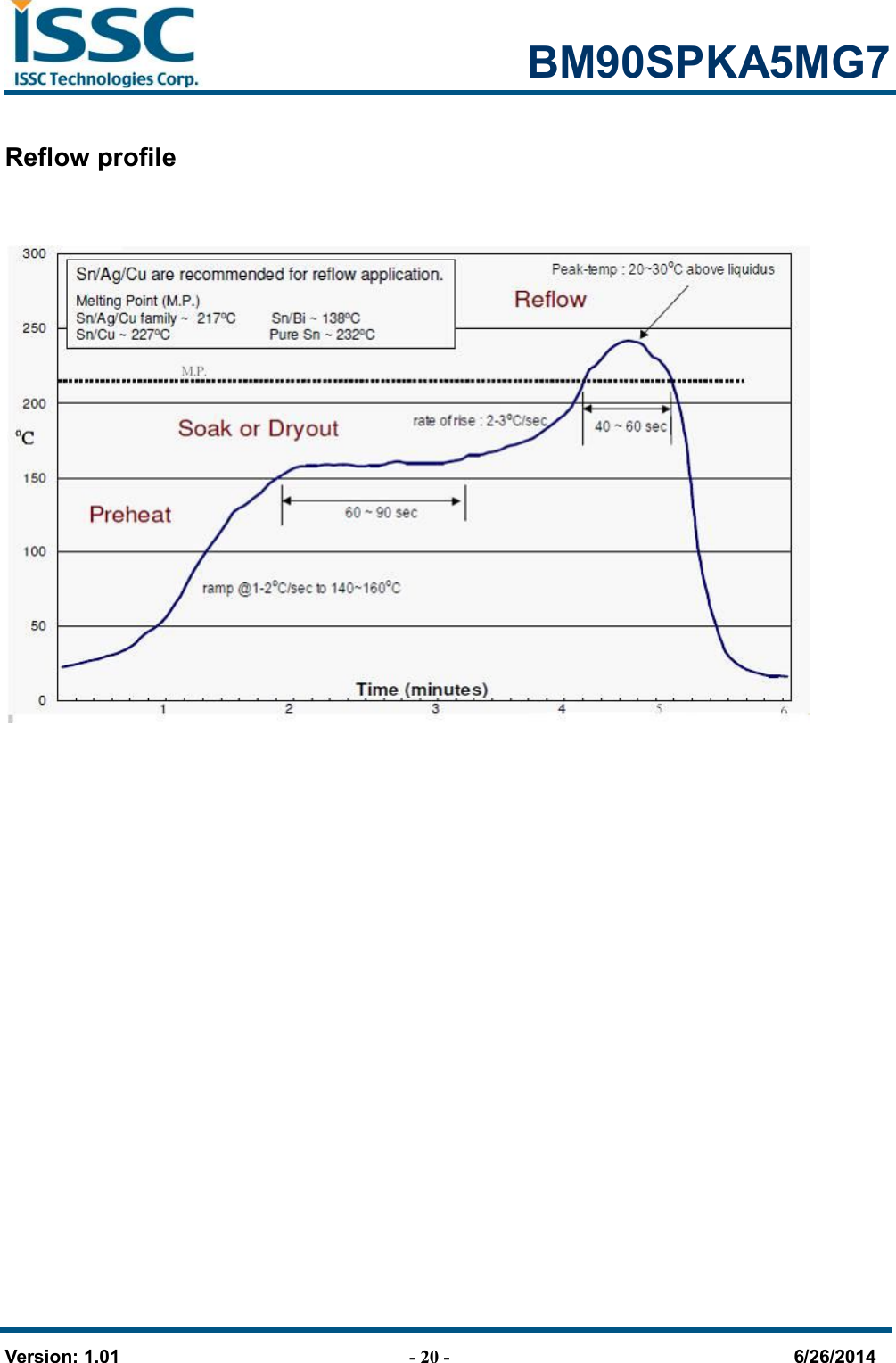
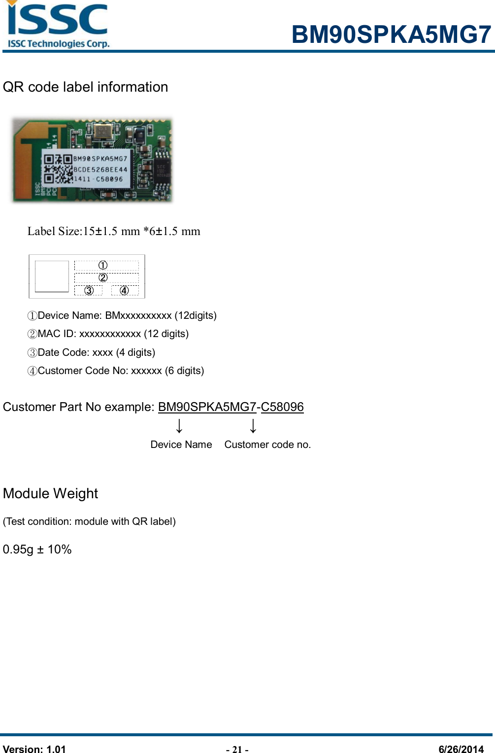
BM90SPK User Manual
Navigation menu
Upload a User Manual
Namespaces
Wiki Guide
HTML
PDF
Info
Views
User Manual
Discussion / Help
Navigation
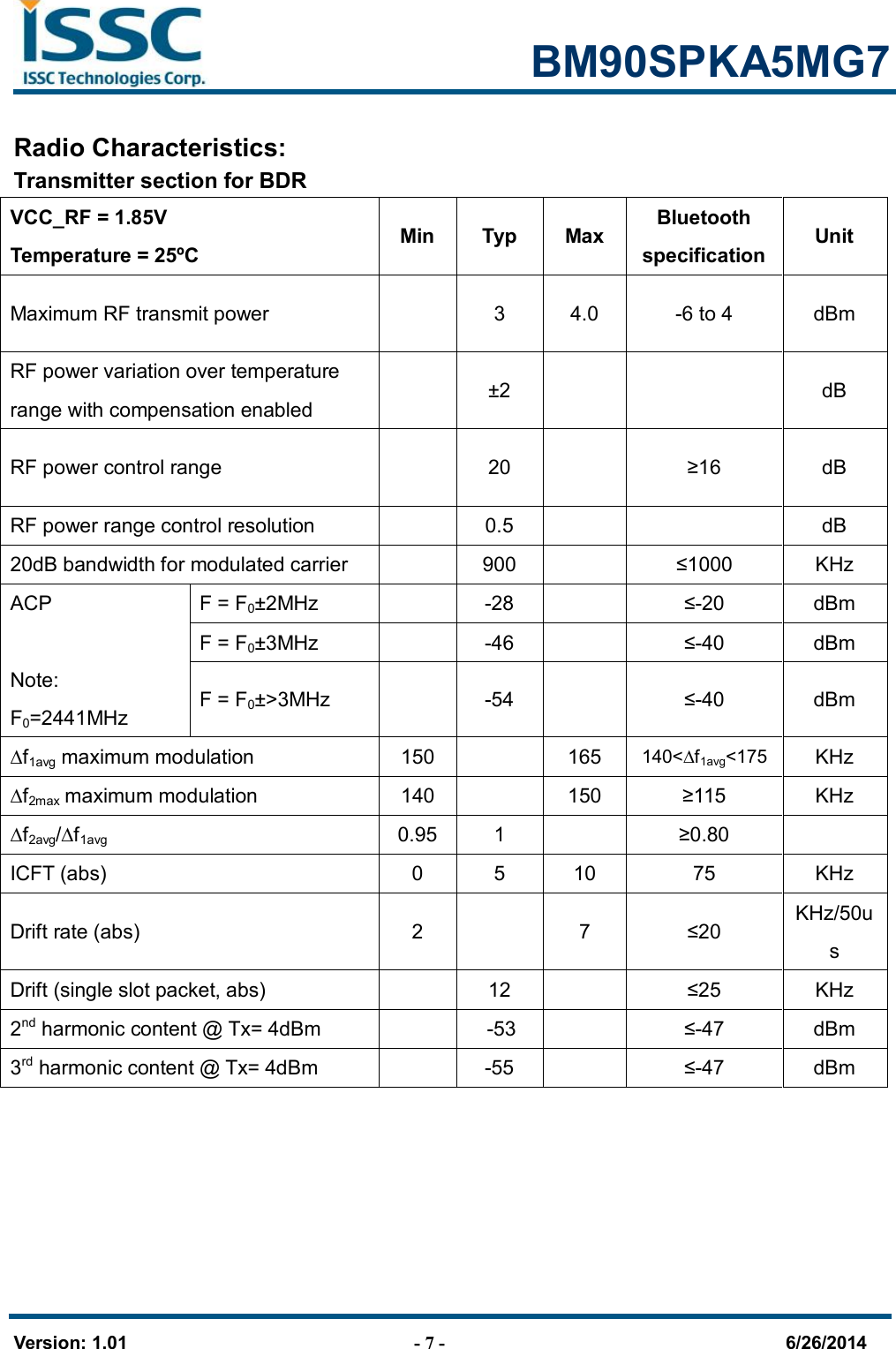
![BM90SPKA5MG7 Version: 1.01 - 6 - 6/26/2014 Electrical Characteristics Absolute Maximum Ratings Rating Min Max Max Operation Temperature -40ºC +85ºC ºC Core supply voltage VDD_CORE, VCC_RF, AVDD_SAR, AVDD_PLL 1.7V 1.98V V Codec supply voltage VDD_AUDIO 3 V I/O voltage VDD_IO 3.3 V Supply voltage BK_VDD 4.3 V 3V1_VIN 5 V BAT_IN 4.3 V ADAP_IN 7.7 V LED[1:0] 5 V Power switch 5 V Recommended Operate Condition Symbol Parameter Min Typical Max Unit VDD18 Digital core supply voltage SAR ADC supply voltage CODEC supply voltage 1.8 1.85 1.95 V VDDIO I/O supply voltage 2.8 3 3.3 V TOPERATION Operating temperature range -20 +25 +70 ºC Tstg Storage temperature -40 +125 ºC VLDO LDO supply voltage 1.8 3.3 V VBAT_IN Supply voltage for Battery_in 3.0 4.2 V](https://usermanual.wiki/TCL-Technoly-Electronics/07/User-Guide-2448546-Page-6.png)