TCL Technoly Electronics 07 Bluetooth Module User Manual BM90SPKA5MG7 101x
TCL Technoly Electronics (Huizhou) Co., Ltd. Bluetooth Module BM90SPKA5MG7 101x
BM90SPK User Manual

BM90SPKA5MG7
5F, No.5, Industry E. Rd. VII, Hsinchu Science Park, Hsinchu city 30077, Taiwan, R.O.C
V
ersion
:
1.0
1
Phone: 886-3-577-8385 6/26/2014
Fax: 886-3-577-8501
BM90SPKA5MG7
Bluetooth 3.0 EDR Audio Module

BM90SPKA5MG7
Version: 1.01 - 2 - 6/26/2014
Product Description
The ISSC BM90SPKA5MG7 is a highly integrated Bluetooth 3.0 EDR stereo
module, designed for high data rate, short-range wireless communication in
the 2.4 GHz ISM band. With the build-in ISSC Bluetooth stack and profile, the
ISSC BM90SPKA5MG7 provides a low power and ultra-low cost Bluetooth
3.0+EDR solution for multi-speaker applications.
Features
Main Chip: ISSC IS1690SM
Bluetooth 3.0 EDR compliant
Max. +4dBm Class 2 output power
Receiver Sensitivity: GFSK typical -90dBm, π/4 PSK typical -91dBm,
8DPSK typical -83dBm
Piconet and Scatter net support
CVSD, A-law, -law CODEC algorithms for voice applications
SBC decode for Bluetooth audio streaming
Build-in High performance stereo audio codec
Microphone input and audio line-in support
Build-in audio mux/gain control for line-in audio signal
Cap-less/single end headphone driver
Audio DAC: 94dB SNR
Build in 350mAH Li-ion battery charger
HSP, HFP, A2DP, AVRCP 1.5 profiles supported
3.3V operating voltage
4Mb Embedded flash program memory and 32Kb EEPROM
37pins for SMT module Size: 15mm x29mm
Build-in PCB Antenna
RoHS compliant
BM90SPKA5MG7
Version: 1.01 - 3 - 6/26/2014
Module Pin out Diagram
BM90SPKA5MG7
P01
35
P16
34
HCI_RXD
33
HCI_TXD
32
P05
31
P37
18
P02
30
P34
17
P24
29
LED2
28
LED1
27
MFB
26
GND
37
BK_OUT
25
SYS_PWR
24
P35
1
P30
3
P20
4
P00
5
P04
6
SPKR
7
SPKL
9
VDDA
10
MIC1_P
11
MIC1_N
12
MIC_BIAS
13
AIR
14
AIL
15
RST
16
SK1
22
ADAP_IN
20
BAT_IN
21
EAN
2P03
36
VDD_IO
19
AOHPM
8
GND
23

BM90SPKA5MG7
Version: 1.01 - 4 - 6/26/2014
Pin Definition
Pin No.
I/O
Name Description
1 I/O
P35 GPIO, default pull-high input
REW button
2 I EAN Embedded ROM/External Flash enable
H: Embedded; L: External Flash
3 P P30 GPIO, default pull-high input
Line-in detection, 1: no line-in detected; 0: line-in detected
4 I/O
P20
GPIO, default pull-high input
System Configuration, H: Application L: Baseband(IBDK
Mode)
5 I/O
P00 GPIO, default pull-low input.
Audio AMP Enable
6 I/O
P04 GPIO, default pull-high input
NFC
7 AO
SPKR R-channel analog headphone output, for cap-less and
single-ended application both
8 AP
AOHPM Headphone common mode output/sense input. Cap-less
application only.
9 AO
SPKL L-channel analog headphone output, for cap-less and
single-ended application both
10 AP
VDDA
Reserve for external cap to fine tune audio frequency
response
11 AI
MIC1_P Mic 1 mono differential analog positive input
12 AI
MIC1_N Mic 1 mono differential analog negative input
13 AP
MIC_BIAS Microphone biasing voltage
14 AI
AIR Stereo analog line in, R-channel
15 AI
AIL Stereo analog line in, L-channel
16 I/O
RST_N System Reset Pin
17 I/O
P34 GPIO, default pull-high input
NFC_SW
18 I/O
P37 GPIO, default pull-high input
FWD button
19 P VDDIO VDDIO pin, for calibration only
Do not add external power to this pin
BM90SPKA5MG7
Version: 1.01 - 5 - 6/26/2014
20 P ADAP_IN Power adaptor input
21 P BAT_IN Battery input
22 I/O
SK1 Default SAR input for battery detection
23 P GND Ground
24 P SYS_PWR System Power Output
25 P BK_OUT Buck feedback sense pin
26 P MFB Multi-Function Push Button key
27 P LED1 LED Driver 1
28 P LED2 LED Driver 2
29 I/O
P24 GPIO, default pull-high input
System Configuration, H: Boot Mode
30 I/O
P02 GPIO, default pull-high input
PLAY/PAUSE button
31 I/O
P05 GPIO, default pull-high input
Phone button
32 O HCI_TXD HCI TX data
33 I HXI_RXD HCI RX data
34 I/O
P16 GPIO, default pull-high input
Volume down button
35 I/O
P01 GPIO, default pull-high input
Volume up button
36 I/O
P03 3rd LED
37 P GND Ground.
BM90SPKA5MG7
Version: 1.01 - 6 - 6/26/2014
Electrical Characteristics
Absolute Maximum Ratings
Rating Min Max Max
Operation Temperature -40ºC +85ºC ºC
Core supply voltage
VDD_CORE, VCC_RF,
AVDD_SAR,
AVDD_PLL
1.7V 1.98V
V
Codec supply voltage
VDD_AUDIO 3 V
I/O voltage VDD_IO 3.3 V
Supply voltage
BK_VDD 4.3 V
3V1_VIN 5 V
BAT_IN 4.3 V
ADAP_IN 7.7 V
LED[1:0] 5 V
Power switch 5 V
Recommended Operate Condition
Symbol Parameter Min Typical Max Unit
VDD18 Digital core supply voltage
SAR ADC supply voltage
CODEC supply voltage
1.8 1.85 1.95 V
VDDIO I/O supply voltage 2.8 3 3.3 V
TOPERATION Operating temperature range -20 +25 +70 ºC
Tstg Storage temperature -40 +125 ºC
VLDO LDO supply voltage 1.8 3.3 V
VBAT_IN Supply voltage for Battery_in 3.0 4.2 V
BM90SPKA5MG7
Version: 1.01 - 7 - 6/26/2014
Radio Characteristics:
Transmitter section for BDR
VCC_RF = 1.85V
Temperature = 25ºC
Min Typ Max Bluetooth
specification
Unit
Maximum RF transmit power
3 4.0 -6 to 4 dBm
RF power variation over temperature
range with compensation enabled ±2 dB
RF power control range
20 ≥16 dB
RF power range control resolution 0.5 dB
20dB bandwidth for modulated carrier 900 ≤1000 KHz
ACP
Note:
F0=2441MHz
F = F0±2MHz -28 ≤-20 dBm
F = F0±3MHz -46 ≤-40 dBm
F = F0±>3MHz -54 ≤-40 dBm
∆f1avg maximum modulation 150 165 140<∆f1avg<175
KHz
∆f2max maximum modulation 140 150 ≥115 KHz
∆f2avg/∆f1avg 0.95 1 ≥0.80
ICFT (abs) 0 5 10 75 KHz
Drift rate (abs) 2
7 ≤20 KHz/50u
s
Drift (single slot packet, abs) 12 ≤25 KHz
2nd harmonic content @ Tx= 4dBm -53 ≤-47 dBm
3rd harmonic content @ Tx= 4dBm -55 ≤-47 dBm

BM90SPKA5MG7
Version: 1.01 - 8 - 6/26/2014
Receiver section for BDR
Temperature = 25ºC Frequency
(GHz) Min Typ Max Bluetooth
specification
Unit
Sensitivity at 0.1% BER for
all basic rate packet types
2.402 -90
≤-70 dBm 2.441 -90
2.480 -90
Maximum received signal at 0.1%
BER
-10 ≥-20 dBm
C/I co-channel 5
≤11 dB
Adjacent channel
selectivity C/I
Note: F0=2441MHz
F =
F0+1MHz -7
≤0 dB
F =
F0-1MHz -7
≤0 dB
F =
F0+2MHz -36
≤-30 dB
F =
F0-2MHz -22
≤-9 dB
F =
F0-3MHz -24
≤-20 dB
F =
F0+5MHz -50
≤-40 dB
F = Fimage -22
≤-9 dB
Maximum level of intermodulation
interferers -38 ≥-39 dB

BM90SPKA5MG7
Version: 1.01 - 9 - 6/26/2014
Transmitter Section for EDR
Temperature = 25ºC Min Typ Max Bluetooth
specification
Unit
Relative transmit power
-1.6
-4 to 1 dB
π/4 DQPSK max
carrier frequency
stability
|ωo|
freq. error 5
≤10 for all
blocks KHz
|ωi|
initial freq.
error
10 ≤75 for all
blocks KHz
|ωo+ωi|
block freq.
error
10 ≤75 for all
blocks KHz
8DPSK max carrier
frequency stability
|ωo|
freq. error 5 ≤10 for all
blocks KHz
|ωi|
initial freq.
error
10
≤75 for all
blocks KHz
|ωo+ωi|
block freq.
error
10 ≤75 for all
blocks KHz
π/4 DQPSK
modulation accuracy
@ Tx= 2dBm
RMS DEVM 7 ≤20 %
99% DEVM
Pass ≤30 %
Peak DEVM 25 ≤35 %
8DQPSK modulation
accuracy @ Tx=
2dBm
RMS DEVM
7 ≤13 %
99% DEVM
Pass
≤20 %
Peak DEVM 20 ≤25 %

BM90SPKA5MG7
Version: 1.01 - 10 - 6/26/2014
In-band spurious
emissions
Note: F0=2441MHz
F > F0+3MHz <-54
≤-40 dBm
F = F0-3MHz -46
≤-40 dBm
F = F0-2MHz -28
≤-20 dBm
F = F0-1MHz -30
≤-26 dBm
F = F0+1MHz -30
≤-26 dBm
F = F0+2MHz -28
≤-20 dBm
F = F0+3MHz -46
≤-40 dBm
EDR differential phase encoding 100 ≥99 %
BM90SPKA5MG7
Version: 1.01 - 11 - 6/26/2014
Receiver Section for EDR
Temperature = 25ºC
Frequency
(GHz)
Modulation
Min Typ Max
Bluetooth
specification
Unit
Sensitivity at 0.01%
BER
2.402 π/4
DQPSK -91
≤-70 dBm
2.441 π/4
DQPSK -91
2.480 π/4
DQPSK
-91
2.402 8DPSK -83
≤-70 dBm
2.441 8DPSK -83
2.480 8DPSK -83
Maximum received signal at 0.1%
BER
π/4
DQPSK -10 ≥-20
dBm
8DPSK -10 ≥-20
C/I co-channel at 0.1% BER
π/4
DQPSK 4 ≤13 dB
8DPSK 5 ≤21 dB
Adjacent channel
selectivity C/I
Note:
F0=2441MHz
F = F0+1MHz
π/4
DQPSK -14 ≤0 dB
8DPSK -8 ≤5 dB
F = F0-1MHz
π/4
DQPSK -13 ≤0 dB
8DPSK -8 ≤5 dB
F = F0+2MHz
π/4
DQPSK -38 ≤-30 dB
8DPSK -34 ≤-25 dB
F = F0-2MHz
π/4
DQPSK -21 ≤-7 dB
8DPSK -21 ≤0 dB

BM90SPKA5MG7
Version: 1.01 - 12 - 6/26/2014
F = F0-3MHz
π/4
DQPSK
-27 ≤-20 dB
8DPSK -20 ≤-13 dB
F = F0+5MHz
π/4
DQPSK -52 ≤-40 dB
8DPSK -45 ≤-33 dB
F = Fimage
π/4
DQPSK -21 ≤-7 dB
8DPSK -21 ≤0 dB
BM90SPKA5MG7
Version: 1.01 - 13 - 6/26/2014
Audio Codec: ADC (MIC PATH/Line-in path)
Test Condition:
T= 25oC, VDD=2.8V, 1KHz sine wave input, Bandwidth = 20~20KHz
Parameter Condition Min. Typ. Max.
Unit
Input full-scale Full scale (line-in) 2.2 Vpp
Resolution 16 bits
Input Sampling Rate 8 48 kHz
SNR fin=1KHz
B/W=20~20KHz
A-weighted
THD+N < 1%
150mVpp input
8KHz 85
dB
16KHz 85
32KHz 85
44.1KHz
85
48KHz 85
SNR A-weighted 1KHz@full scale,
Microphone boost enable
75 dB
THD+N (Mic input)
@30mVrms input
0.04 %
THD+N (line input) 0.01 %
Mic Boost Gain 20 dB
Digital Gain -54 4.85 dB
Analog Gain 26 dB
Digital Gain Step 6 dB
Analog Gain Step 1.7 dB
Input impedance
(microphone mode)
Input impedance 6 10 KΩ
Input capacitance 20 pF
Analog supply voltage
(AVDD) 1.8 2.8 3.0 V
BM90SPKA5MG7
Version: 1.01 - 14 - 6/26/2014
Audio Codec: DAC (SPEAKER path)
Test Condition: T= 25oC, VDD=2.8V, 1KHz sine wave input, Bandwidth= 20~20KHz
Parameter Condition Min. Typ. Max.
Unit
Output Level Full scale 2.1 Vpp
Resolution 16 bits
Output Sampling Rate 8 48 KHz
SNR fin=1KHz
B/W=20~20KHz
A-weighted
THD+N < 0.01%
0dBFS signal
Load=100KΩ
8KHz 94 dB
16KHz 94 dB
32KHz 94 dB
44.1KHz 94 dB
48KHz 94 dB
Max Output Power
RL=16Ohm 35 mW
RL=32Ohm 17 mW
THD+N
16Ohm load 0.05 %
100KΩ load 0.01 %
Digital Gain -54 4.85 dB
Digital Gain Resolution
6 dB
Analog Gain -28 3 dB
Analog Gain step 1 dB
Output resistance RL 8 16 Ohm
Output capacitance Cp 500 pF
Crosstalk between
channels
L vs. R, measured at
-10dBFS@1KHz input -90 -80 dB
Analog supply voltage
(AVDD) 1.8 2.8 3.0 V
BM90SPKA5MG7
Version: 1.01 - 15 - 6/26/2014
Battery Charger
Charging Mode (BAT_IN rising to 4.2V) Min Typ Max Unit
Operation Temperature -10 55 ℃
Input Voltage (Vin)
Note: It needs more time to get battery fully
charged when Vin=4.5V
4.5 7 V
Battery trickle charge current
(BAT_IN < trickle charge voltage threshold)
0.1C mA
Trickle charge voltage threshold 3 V
Maximum battery
charge current
Headroom > 0.7V 350 mA
Headroom = 0.3V 150 mA
Minimum battery
charge current
Headroom > 0.7V 1 mA
Headroom = 0.3V 1 mA
Battery charge termination current,
% of fast charge current
10
%
Battery recharge hysteresis (Note1) 100 mV
Battery recharge current (Note2)
Note: C Battery capacity 0.25C mA
Note1:When charging complete and the adapter is still in, the battery voltage will slowly drop down.
When the voltage drop is larger than 100mV from the full voltage, the re-charging cycle will
start.
Note2:If the battery voltage during plug in is larger than 4V, the charging current will be limited to
0.25C to avoid the battery voltage overshoot.
BM90SPKA5MG7
Version: 1.01 - 16 - 6/26/2014
Clock
Parameters MIN TYP MAX Unit
Crystal Frequency 16 MHz
Frequency Tolerance 20 ppm
Operating Temperature -20 70 OC
Trimming Capacitance 6.4 pF
Trimming Step Size 0.2 pF
Digital GPIO
Parameters MIN TYP MAX Unit
Input Voltage 2.7 3 3.6 V
VIH (Input High Voltage) 2.0 Vdd V
VIL (Input Low Voltage) 0 0.8 V
Input Reference Resistor
RPU (Pull-Up Resistor) 50K Ohm
RPD (Pull-Down Resistor) 50K Ohm
Output Voltage
VOH (Output High Voltage) 2.4 Vdd V
VOL (Output Low Voltage) 0 0.4 V
BM90SPKA5MG7
Version: 1.01 - 17 - 6/26/2014
Current Consumption Flash version
Single Mode
Test Condition: T= 25oC, BAT_IN=4.0V, with flash code, codec without loading
Normal Operation Min Typ Max Unit
Off mode 5.6 uA
Standby mode 1 mA
Link mode 0.9 mA
SCO link 23.5 mA
A2DP link 26.9 mA
Twin Mode
Test Condition: T= 25oC, BAT_IN=4.0V, with flash code, codec without loading
Normal Operation Min Typ Max Unit
Off mode 5.6 uA
Standby mode 1.3 mA
Link mode 1.1 mA
SCO link 25.8 mA
A2DP link 34 mA

BM90SPKA5MG7
Version: 1.01 - 18 - 6/26/2014
Antenna performance
Parameters MIN TYP MAX Unit
Antenna gain 1.76 dBi
Efficiency 70 80 %
BM90SPKA5MG7
Version: 1.01 - 19 - 6/26/2014
Outline Dimension (Module Foot print)
BM90SPKA5MG7
Version: 1.01 - 20 - 6/26/2014
Reflow profile
BM90SPKA5MG7
Version: 1.01 - 21 - 6/26/2014
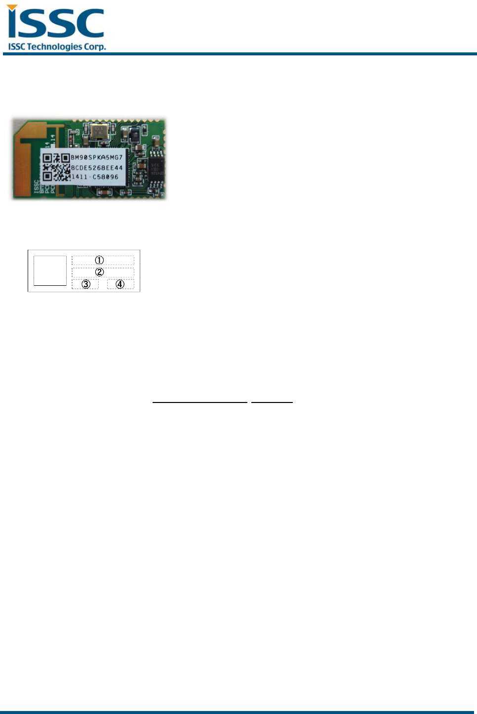
QR code label information
Label Size:15±1.5 mm *6±1.5 mm
①Device Name: BMxxxxxxxxxx (12digits)
②MAC ID: xxxxxxxxxxxx (12 digits)
③Date Code: xxxx (4 digits)
④Customer Code No: xxxxxx (6 digits)
Customer Part No example: BM90SPKA5MG7-C58096
↓ ↓
Device Name Customer code no.
Module Weight
(Test condition: module with QR label)
0.95g ± 10%

BM90SPKA5MG7
Version: 1.01 - 22 - 6/26/2014
Storage standard
1. Calculated shelf life in sealed bag: 12 months at < 40 ℃ and <90% relative humidity (RH)
2. After bag is opened, devices that will be subjected to reflow solder or other high temperature process
must be Mounted within 168 hours of factory conditions <30℃/60% RH

BM90SPKA5MG7
Version: 1.01 - 23 - 6/26/2014
Ordering Information
Device
Module
Order Number
Size Shipment
Method
BM90SPKA5MG7
Bluetooth 3.0 EDR
Wireless Speaker Module
29*15 mm Tray
Note:
Minimum Order Quantity is 630pcs Tray.
BM90SPKA5MG7
Version: 1.01 - 24 - 6/26/2014
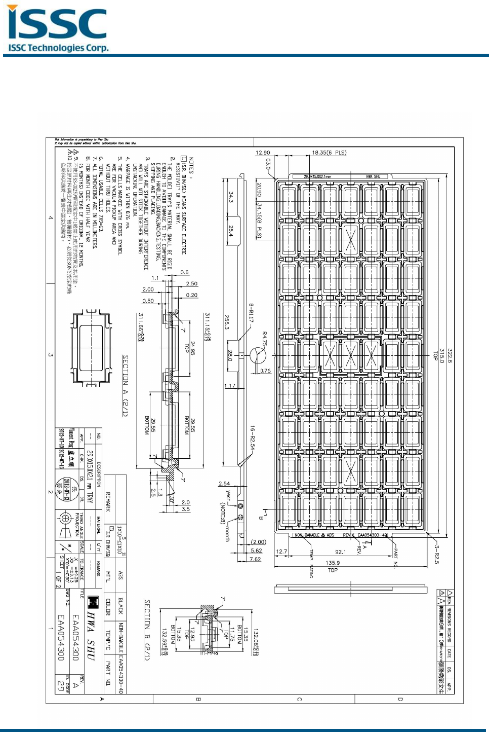
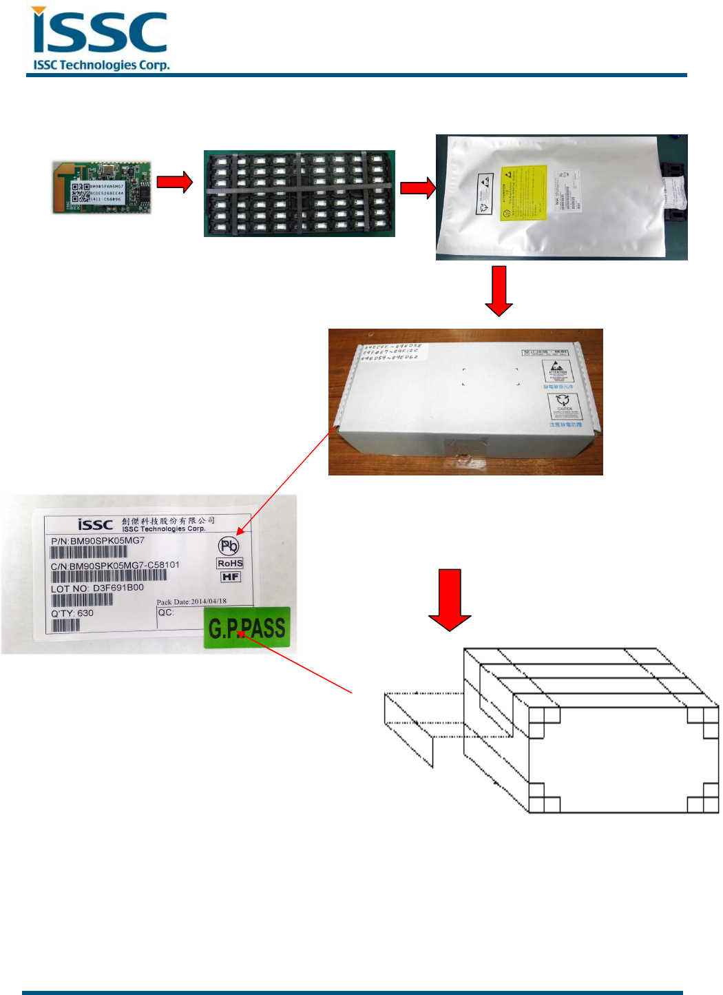
Packing Information
Tray Dimensions
BM90SPKA5MG7
Version: 1.01 - 25 - 6/26/2014
Packing Method
Inner box: Q’ty (630 Pcs)
Dimensions: 36*16*9.5 cm
Bar Code Label Example
P/N: Part No.(device name)
C/N: Customer Part No.(Part no. - customer code no.)
Lot No: Lot ID
Q’ty: box or Carton Module’s Q’ty
Carton: Q’ty (3780 Pcs)
Dimensions: 38*35*30 cm
Ho
w
w
tofixtheBTmodel
B
B
M90SPKt
o
1、Everym
o
2、FixtheB
T
3、Everypi
n
1、Main
b
o
SRS‐X11
o
delhas37p
T
modeltoS
R
n
isfixedont
b
oardisfixed
1、
B
2、
T
in;
R
S‐X11main
hemainboa
r
toSRS‐X11
b
B
M90SPKBT
M
T
hegainofP
C
boardbyits
3
r
dbytin.
b
ytheScrew
Modelconta
C
BAntennai
s
37pin;
insPCBAnte
n
s
about1.76
d
n
na;
d
Bi;
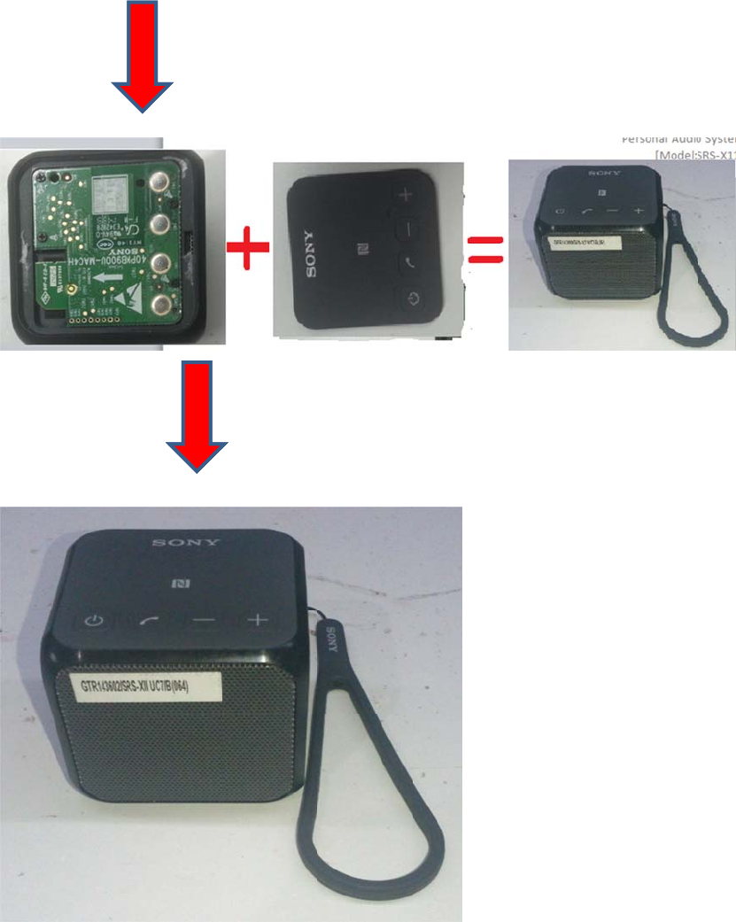
SRS
‐
FC
C
Cha
n
voi
d
Thi
s
con
d
any
IC
S
Thi
s
to t
h
mus
t
‐
X11
C
Statement
n
ges or mod
i
d
the user's a
u
s
device com
p
d
itions: (1) t
h
interference
r
S
tatement
s
device com
p
h
e following
t
t accept any
i
i
fications not
u
thority to op
p
lies with Pa
r
h
is device ma
y
r
eceived, inc
l
p
lies with In
d
t
wo conditio
n
i
nterference,
expressly ap
p
e
rate the equ
i
r
t 15 of the F
C
y
not cause
h
l
uding interf
e
d
ustry Canad
a
n
s: (1) this d
e
including int
proved by th
e
ipment
CC Rules. O
p
h
armful inter
f
e
rence that
m
a
licence-ex
e
e
vice may no
t
t
erference th
a
e
party respo
n
p
eration is s
u
f
erence, and
(
m
ay cause un
d
mpt RSS sta
n
t
cause inter
fe
a
t may cause
u
n
sible for co
m
u
bject to the
f
(
2) this devic
e
d
esired opera
t
n
dard(s). Op
e
e
rence, and (
2
u
ndesired op
e
m
pliance co
u
f
ollowing tw
o
e
must accep
t
t
ion.
e
ration is sub
j
2
) this devic
e
eration of th
e
u
ld
o
t
j
ect
e
e
device.
Le présent appareil est conforme aux CNR d'Industrie Canada applicables aux appareils radio
exempts de licence. L'exploitation est autorisée aux deux conditions suivantes : (1) l'appareil ne
doit pas produire de brouillage, et (2) l'utilisateur de l'appareil doit accepter tout brouillage
radioélectrique subi, même si le brouillage est susceptible d'en compromettre le fonctionnement.
The end host device should bear the label which indicate "Contains FCC ID:ZVA07" or
"Contains IC:9976A-07".