TESSERA TECHNOLOGY 0001 ZigBee RF4CE Module Board User Manual TK RF8058 SB UM E
TESSERA TECHNOLOGY INC. ZigBee RF4CE Module Board TK RF8058 SB UM E
User Manual
- 1 -
Date published: March 8, 2010
Rev. 5.0
© TESSERA TECHNOLOGY INC.
Printed in Japan
User’s Manual
TK-RF8058+SB
ZigBeeTM/RF4CETM-ready
Wireless Network Evaluation Board

- 2 -
Welcome to the world of TK-RF8058+SB.
You are now being navigated to the design environment
of the μPD78F8058 microcontroller for developing
wireless network applications. Please follow the tutorial
step by step.
- 3 -
[NOTES]
The information in this document is subject to change without notice. No part of
this document may be copied or reproduced in any form or by any means without
the prior written consent of TESSERA TECHNOLOGY INC.
TESSERA TECHNOLOGY INC. assumes no liability for infringement of patents or
copyrights of third parties by or arising from use of a product described herein.
This product is designed and manufactured with intention for use in evaluation
and prototyping by engineers with knowledge of security, safety and reliability.
TESSERA TECHNOLOGY INC. would like to inform, that the standard quality
assurance procedure(s) have not been fully applied to this product and its
documentation and that TESSERA TECHNOLOGY INC. cannot assure the full
and error free function and/or the standard quality level.
[CAUTION]
This equipment should be handled like a CMOS semiconductor device. The user
must take all precautions to avoid build-up of static electricity while working with
this equipment. All test and measurement tool including the workbench must be
grounded. The user/operator must be grounded using the wrist strap. The
connectors and/or device pins should not be touched with bare hands.

- 4 -
[FCC WARNING & NOTICE]
●Changes or modifications not expressly approved by the party responsible for
compliance could void the user’s authority to operate the equipment.
●The intended use of the product is generally not for the general public.
It is generally for industry/commercial use by the professional electric engineer.
To be in compliance with FCC 15.203 requirements, the product must be
installed by professional installers with approved antenna that was included in
the product.
Class B:
This equipment has been tested and found to comply with the limits for a Class B
digital device, pursuant to part 15 of the FCC Rules. These limits are designed to
provide reasonable protection against harmful interference in a residential
installation. This equipment generates, uses and can radiate radio frequency
energy and, if not installed and used in accordance with the instructions, may
cause harmful interference to radio communications. However, there is no
guarantee that interference will not occur in a particular installation. If this
equipment does cause harmful interference to radio or television reception, which
can be determined by turning the equipment off and on, the user is encouraged to
try to correct the interference by one or more of the following measures:
● Reorient or relocate the receiving antenna.
● Increase the separation between the equipment and receiver.
● Connect the equipment into an outlet on a circuit different from that to which the
receiver is connected.
● Consult the dealer or an experienced radio/TV technician for help.
This device complies with Part 15 of the FCC Rules. Operation is subject to the
following two conditions:
●this device may not cause harmful interference, and
●this device must accept any interference received, including interference that
may cause undesired operation.
●The host device shall also comply with the certification labeling requirements of
each of the modules it contains.
●A reference to the enclosed module displaying its FCC ID certification number.
Recommended wording:
Contains FCC ID: X8U0001
- 5 -
Contents
1 INTRODUCTION........................................................................................... 8
2 PREPARATIONS........................................................................................ 10
2.1 Development Tools, Sample Programs, and the MAC Library.................................. 11
2.1.1 Integrated Development Environment PM + V6.31 .......................................................... 11
2.1.2 Device file DF788058 e1.00b ........................................................................................... 11
2.1.3 C Compiler CC78K0R W2.12 : Code size limited version................................................ 11
2.1.4 Assembler RA78K0R W1.33 : Code size limited version ................................................. 11
2.1.5 78K0R integrated debugger ID78K0R-QB V3.60............................................................. 11
2.1.6 Built-in Flash Memory Writing Program WriteEZ5............................................................ 11
2.1.7 78K0R Starter Kit Setting.................................................................................................. 11
2.1.8 Starter kit USB driver ........................................................................................................ 12
2.1.9 The RF Test Program....................................................................................................... 12
2.2 Installation of Software Development Tools............................................................... 13
2.2.1 Start-up of the installation CD-ROM ................................................................................. 13
2.2.2 Installation of the software development tools.................................................................. 13
2.2.3 Uninstall ............................................................................................................................ 20
2.2.4 File Configuration in PC.................................................................................................... 21
2.3 USB Driver .................................................................................................................... 22
2.3.1 Install to Windows XP ....................................................................................................... 23
2.3.2 Install to Windows2000..................................................................................................... 26
2.3.3 Confirmation of the installation ......................................................................................... 30
2.4 Sample Environment .................................................................................................... 31
2.4.1 Installation of the sample programs.................................................................................. 32
2.4.2 File Configuration of the sample program ........................................................................ 34
3 EXPERIENCES........................................................................................... 35
3.1 Starting PM + ................................................................................................................ 37
3.2 Introduction to PM +..................................................................................................... 38
3.3 Loading Workspace (Project) ...................................................................................... 40
3.4 Configuration of Linker Option.................................................................................... 42
3.4.1 "Output1" Tab ................................................................................................................... 42
3.4.2 "Output2" Tab ................................................................................................................... 44
- 6 -
3.5 Configuration of Compiler Option............................................................................... 45
3.5.1 "Extend" Tab..................................................................................................................... 45
3.5.2 "Startup Routine" Tab ....................................................................................................... 46
3.6 Configuration of Debugger setting ............................................................................. 47
3.7 TK board setting ........................................................................................................... 49
3.8 Creating execution format ........................................................................................... 50
3.9 Starting integrated debugger (ID78K0R-QB) .............................................................. 52
3.10 Introduction of the integrated debugger (ID78K0R-QB)........................................... 57
3.11 Executing a program.................................................................................................... 58
3.12 Stop a program ............................................................................................................. 59
3.13 Terminating integrated debugger (ID78K0R-QB) ....................................................... 60
3.14 The RF Test Program ................................................................................................... 61
3.14.1 Procedure for one to one transmit/receive test .............................................................. 61
3.14.2 PER test / receiver.......................................................................................................... 73
3.14.3 Continuous TX / Pseudo Noise ...................................................................................... 73
3.14.4 Continuous TX / Raw carrier .......................................................................................... 73
3.14.5 RX Mode......................................................................................................................... 73
3.14.6 IDLE MODE .................................................................................................................... 73
3.14.7 Standby MODE............................................................................................................... 73
3.14.8 Deep Sleep mode........................................................................................................... 73
3.14.9 Power down mode.......................................................................................................... 73
3.14.10 Set RF channel ............................................................................................................. 74
3.14.11 Manually set UZ2400 register....................................................................................... 74
3.14.12 Resetting RF................................................................................................................. 74
3.15 Terminating PM +.......................................................................................................... 75
4 HARDWARE SPECIFICATIONS................................................................ 76
4.1 Layout of hardware functions...................................................................................... 77
4.2 Hardware Functions ..................................................................................................... 78
4.2.1 SW4 (Dip Switch).............................................................................................................. 78
4.2.2 SW5 .................................................................................................................................. 78
4.2.3 SW6 .................................................................................................................................. 78
4.2.4 JP1.................................................................................................................................... 78
4.2.5 JP2.................................................................................................................................... 78
- 7 -
4.2.6 JP3 ..................................................................................................................................... 79
4.2.7 JP4 ..................................................................................................................................... 79
4.2.8 JP5 ..................................................................................................................................... 79
4.2.9 SW1,SW2,SW3...................................................................................................................... 79
4.2.10 SW7................................................................................................................................... 79
4.2.11 LED4 ................................................................................................................................. 80
4.2.12 LED1, LED2, and LED3....................................................................................................... 80
4.2.13 FP1 ................................................................................................................................... 80
4.2.14 J2 and J3 .......................................................................................................................... 80
4.3 Summary of Power Supply Settings ........................................................................... 80
4.4 Solder-short pad........................................................................................................... 81
5 TROUBLESHOOTING................................................................................ 82
5.1 If you cannot find USB driver when you connect PC to the kit................................. 82
5.2 Error when you start the debugger ............................................................................. 82
5.2.1 "Can not communicate with Emulator..." (F0100 or A0109)............................................. 83
5.2.2 "Incorrect ID Code." (Ff603) ............................................................................................. 83
5.2.3 "The on-chip debug function had been disabled in the device." (F0c79) ......................... 84
5.2.4 "Disabling the on-chip debug function is prohibited." (F0c33).......................................... 84
6 OTHER INFORMATION ............................................................................. 85
6.1 Create a new workspace .............................................................................................. 86
6.2 Registration of new source files.................................................................................. 91
6.3 Debugger tips ............................................................................................................... 93
6.3.1 Change display of buttons ................................................................................................ 93
6.3.2 Display source list and function list................................................................................... 93
6.3.3 Set/delete breakpoints...................................................................................................... 94
6.3.4 Display global variables.................................................................................................... 95
6.3.5 Display global variables while programs are running ....................................................... 96
6.3.6 Display local variables ...................................................................................................... 97
6.3.7 Display memory and SFR contents .................................................................................. 97
6.4 Erase of flash memory ................................................................................................. 98
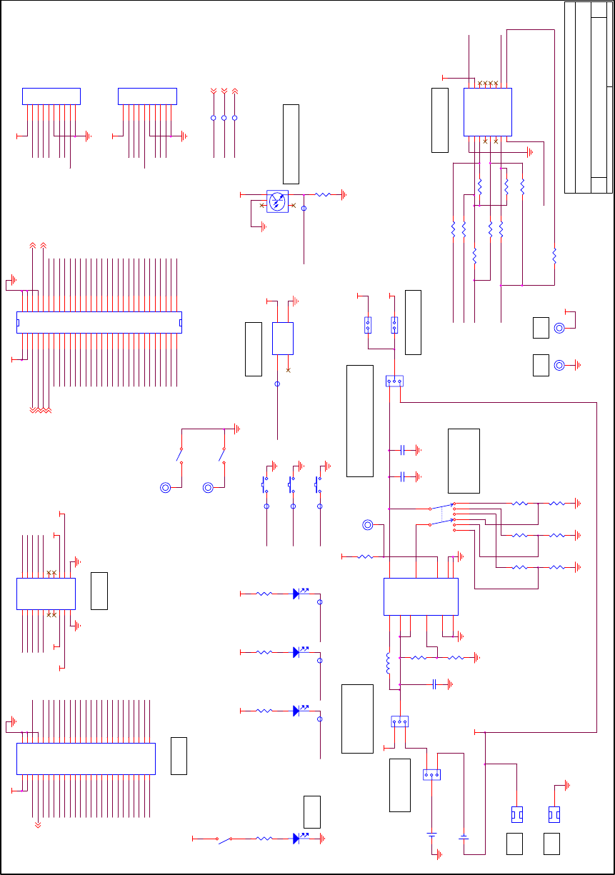
6.5 BOM List, Circuit diagram & Pin Connection ........................................................... 104
7 MODE SETTING OF THE BOARD........................................................... 110

- 8 -
1 Introduction
Target Reader Software development engineers who wish to become
familiar with the development environment of the 78K0R
microcontrollers. It is assumed that the readers have been
familiar with basics of microcontrollers, C and assembler
languages, and the WindowsTM operating system.
Purpose For readers to become familiar with the design environment
and the application examples of wireless networks.
Overview This manual consists of the following contents
Chapter 1 Introductions
→Overview of this manual
Chapter 2 Preparations
→Introduction of soft tools, and sample programs and installation
Chapter 3 Experiences
→ Guide to the basic operations of PM + and the integrated
debugger using sample programs.
Chapter 4 Hardware Specifications
→Explain the hardware of TK-RF8058+SB
Chapter 5 Troubleshooting
→Describe how to solve troubles you may face, such as errors when
starting the integrated debugger (ID78K0R-QB)
Chapter 6 Other Information
→Introduce other information, such as how to create a new
workspace (project) on integrated development environment (PM+),
how to register additional source file, and some useful tips of the
integrated debugger.
The circuit diagrams of demonstration kit are included in this
chapter.
Chapter 7 Mode Setting of the Board
→ Explanation of switch setting.
- 9 -
Trademark Microsoft and Windows are either registered trademarks or
trademarks of Microsoft Corporation in the United States and/or
other countries.
Adobe and Acrobat are trademarks of Adobe Systems
Incorporated (Adobe System Incorporated).
Other company names and product names that appear in this
document are the registered trademarks or trademarks of their
respective companies.

- 10 -
2 Preparations
This chapter introduces the development environment and describes how to
install the sample programs. The sample program can be tested on this
hardware platform of the evaluation kit.

- 11 -
2.1 Development Tools, Sample Programs, and the MAC Library
This section outlines the development tools, sample programs and the MAC
library used in this tutorial.
2.1.1 Integrated Development Environment PM + V6.31
This is a project manager, where you work for editing the source code,
compiling it, and initiating the debugger. The project manager works on MS
Windows 2000 or XP.
2.1.2 Device file DF788058 e1.00b
A device file contains an MCU specific information. It instructs the
development tools what kind of an MCU the tools shall work for.
2.1.3 C Compiler CC78K0R W2.12 : Code size limited version
This is a free compiler for the 78K0R microcontrollers. The object code size
is limited to 64 Kbytes. It works on MS Windows 2000 or XP.
2.1.4 Assembler RA78K0R W1.33 : Code size limited version
This is a free assembler for the 78K0R microcontrollers. The object code
size is limited to 64 Kbytes. It works on MS Windows 2000 or XP. The
RA78K0R Assembler Package contains Structured Assembler
Preprocessor, Assembler, Linker, Object Converter, Librarian, and List
Converter.
2.1.5 78K0R integrated debugger ID78K0R-QB V3.60
The Integrated Debugger ID78K0R-QB offers a debug environment on
your PC, where the MS Windows 2000 or XP runs, if the TK board is
connected to the PC with USB. The USB I/F accesses to the OCD, On
Chip Debug, interface on the microcontroller.
2.1.6 Built-in Flash Memory Writing Program WriteEZ5
This is the Windows software to write programs on built-in flash memory.
By connecting TK-RF8058+SB and PC with bundled USB cable, you can
write/delete programs on the built-in flash memory.
2.1.7 78K0R Starter Kit Setting
If you forget about the security ID or if you set “Does not erases data of
flash memory in case of failures in enabling on-chip debugging”, you can
- 12 -
erase the flash memory by using this starter kit.
2.1.8 Starter kit USB driver
This is a software driver for PC to access to the USB interface of the
TK-RF8058+SB board.
2.1.9 The RF Test Program
The RF Test Program is used in [chapter 3 Experiences].
The RF Test Program is provided in the form of the C source codes.
If you wish to tailor the RF Test Program to meet your specific needs, you
can edit the source code, re-compile it with debug build to generate a load
module file, then, start the debugger to load the tailored execution code on
to the microcontroller for further debugging on the project manager PM +.
Alternatively, if debugging is not required, you can make a release build to
achieve a new hex file, on the project manager PM +.
As a general remark, please respect your local regulation of
electro-magnetic emission. In general, it is suggested to use the
TK-RF8058+SB board in a radio anechoic chamber.
- 13 -
2.2 Installation of Software Development Tools
2.2.1 Start-up of the installation CD-ROM
The attached CD-ROM contains Development Tools, documents and sample
soft ware.
You can install it using an installer.
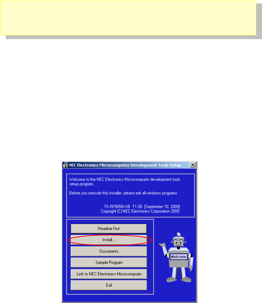
2.2.2 Installation of the software development tools.
Please insert the CD-ROM in the drive. The installer will show up automatically.
If it does not start automatically, please initiate it by double clicking the
SETUP.EXE.
<1> Readme First
The contents of the CD-ROM, and some notes are available.
Please read it at first.
<2> Install…
Click “Install” to start installation of development tools.
For details, please refer to the next section.
- 14 -
<3> Documents
Manuals of development tools and the evaluation kit are available in PDF
files.
When this button is clicked, the WWW browser will start. Adobe® Acrobat®
Reader is available in the CD-ROM.
<4> Sample Program
Click this button to start the WWW browser for the sample program and the
tutorial.
<5> Link to NEC Electronics Microcontrollers
Click this button to start the WWW browser display the link to the NEC
Electronics Microcontroller web site
(http://www.necel.com/micro/index_e.html)
The NEC Electronics Microcontroller web page provides with the latest
product/tool information and FAQs.
<6> Exit
Terminate the setup.
- 15 -
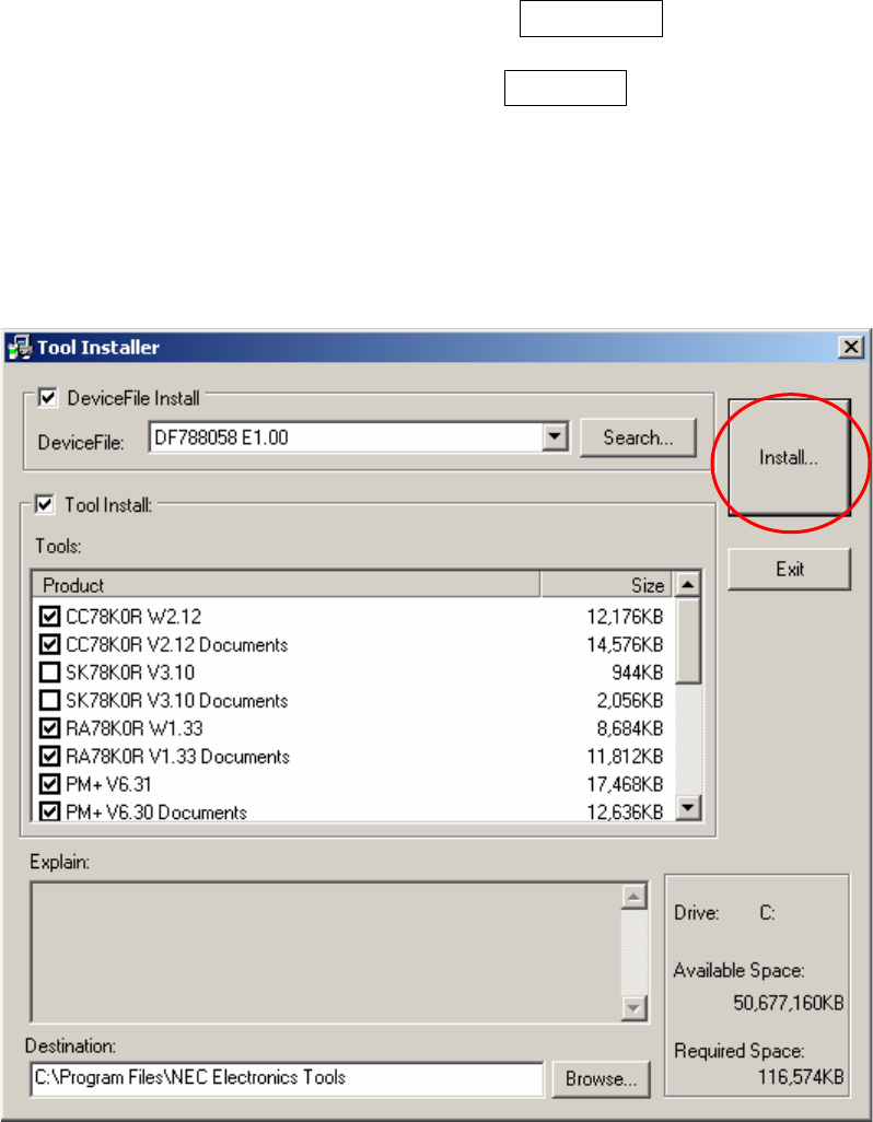
① Select products that you need to install.
(as default, all the products that you need to use the demostration kit
are selected.)
"Explain" area displays an explanation of the selected product.
To change the installation destination, click Browse… .
When all the settings are completed, click Install… .
* In this document, it is assumed that users install the programs under "NEC
Electronics Tools" directory (default installation directory). Users can find the
tools by selecting “Start Menu” -> "Programs" -> "NEC Electronics Tools".
- 16 -
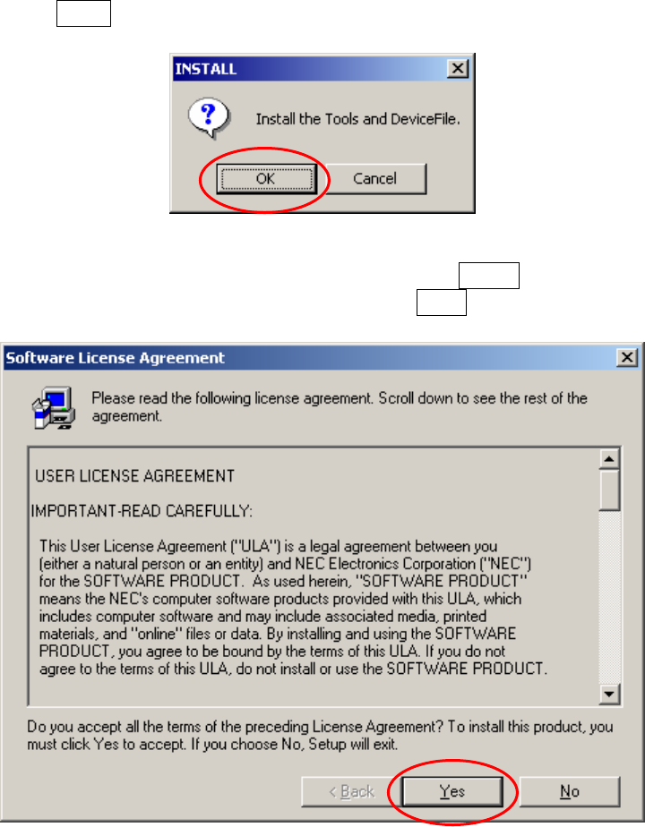
② Click OK when "Install" comfirmation dialog box is opened.
③ Read "software license agreement" and click Yes for continuing the
installation.To stop the installation, click No .
- 17 -
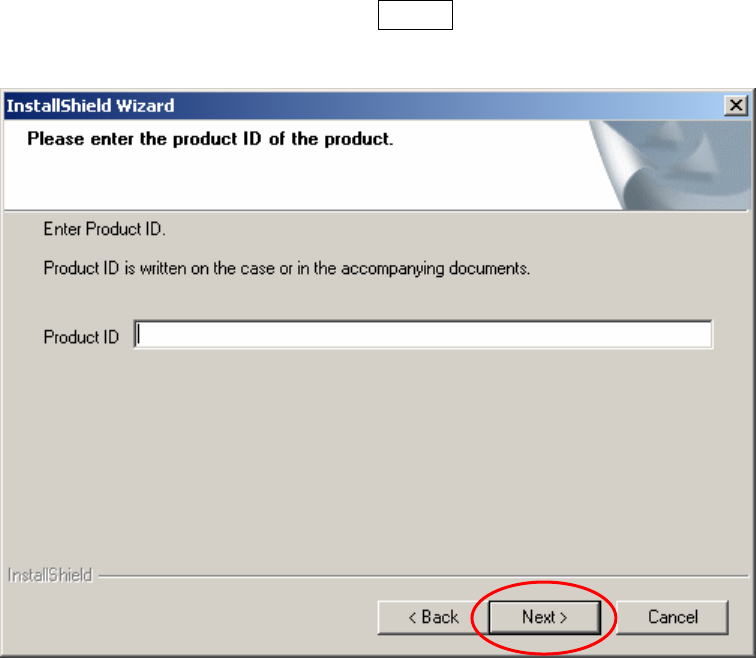
④ Enter the product ID, and click Next .
* The product ID is available on the “README.html” the other sheet.
⑤ It starts copying the files.
- 18 -
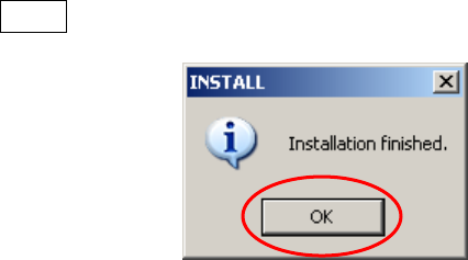
⑥ When the installation is completed, the following dialog opens.
Click OK .
⑦ "NEC Electronics Starter Kit Virtual UART" USB driver must be installed on
PC before you connect to TK-RF8058+SB . Install the USB driver by
referring "2.3USB Driver".

- 19 -
Notes on the installation authority
To install this tool in Windows 2000 or XP, the authority of a administrator is
necessary. Therefore, please login as an administrator.
Notes on the install-directory
Please do not use 2-byte characters, such as umlaut in the directory name,
where the product is to be installed.
Note on the version of Windows
If the language of the Windows is not English, a file transfer error during
installation might be observed. In this case, please abort the installation in
the language, and re-install it in an English version of Windows.
The identical problem may be observed, if a language other than English is
specified as the system language in the “Regional Settings Properties” tab.
- 20 -
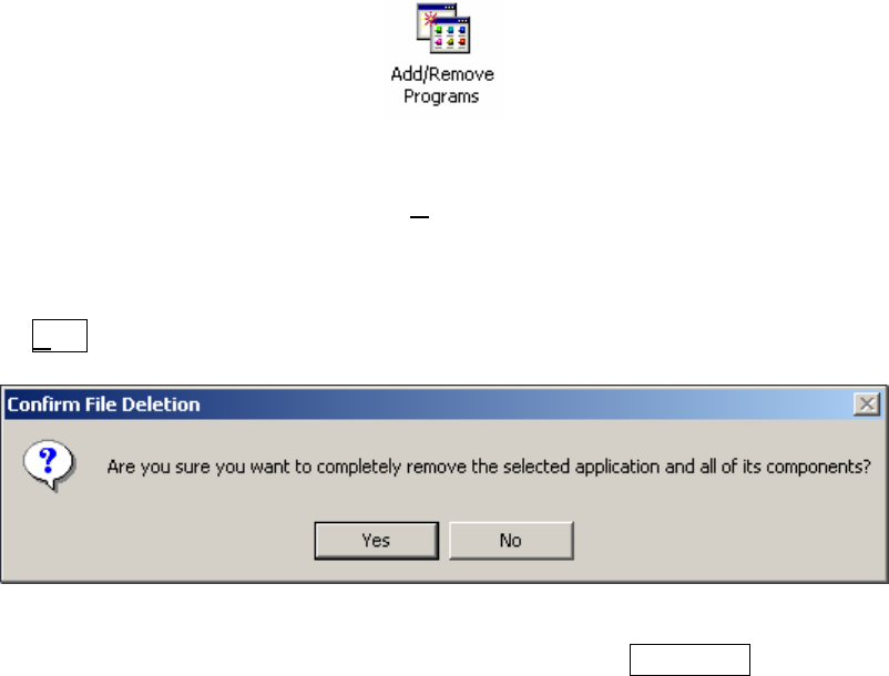
2.2.3 Uninstall
<1> Start "Add /Remove Programs" in the Control Panel.
(Example here is based on Windows2000)
<2> Select the tool that you want to uninstall from the list displayed in
"Install/Uninstall" and click [Add/Remove...].
<3> A dialog box for confirming deletion of files will be displayed. Click
Yes . Deleting of the files will be started.
<4> When the completion message is displayed, click OK .
Caution:
Deletion of some files may be asked during uninstallation. Normally,
deletion of these files causes no problem.
<5> This completes uninstalling this tool.
- 21 -
2.2.4 File Configuration in PC
Software Development Tools are installed in "C:¥Program Files¥NEC Electronics
Tools" on default setting.
When you use the tools, please open the tools from [Start menu] ->
[Programs]->[NEC Electronics Tools].

- 22 -
2.3 USB Driver
You need to install “NEC Electronics Starter Kit Virtual UART” in your PC.
When TK-RF8058+SB is used, it is necessary to install the “NEC Electronics Starter Kit
Virtual UART” driver in the host machine. Please install the driver according to the following
procedures with appending CD in the drive.
"Starter Kit USB Driver" must be installed on the PC. If not, please refer to "2.2 Installation of
Software Development Tools" to install the “Starter Kit USB Driver” first.
Attention Do not use a USB hub for connecting TK-RF8058+SB .
Depending on the version of Windows OS, the installation will be differed.
Please check your Windows version, and follow the instructions
- Windows XP -> "2.3.1Install to Windows XP"
- Windows 2000 -> "2.3.2Install to Windows2000"
After the installation, go to "2.3.3Confirmation of the installation"
- 23 -
2.3.1 Install to Windows XP
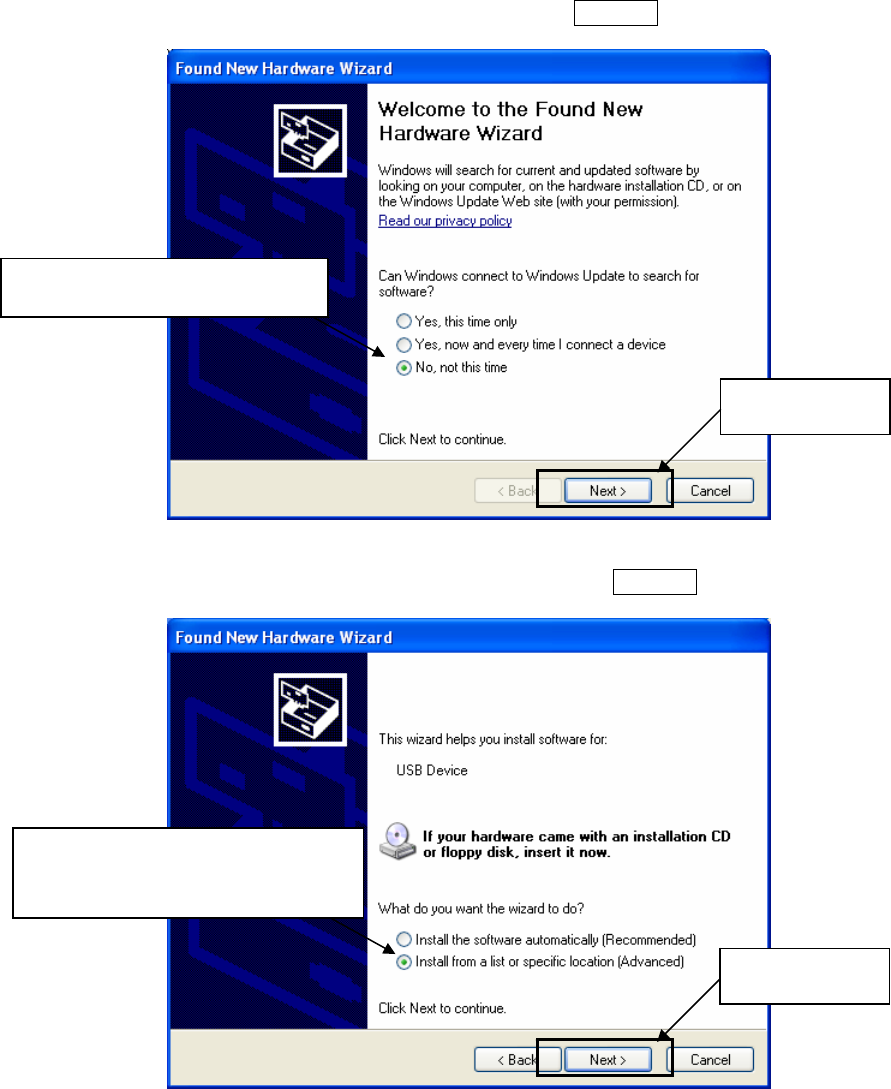
1. Once the TK-RF8058+SB is connected with USB, the "Found New Hardware Wizard"
will be started. Select "No, not this time" and click Next > .
2. Select "Install from a list or specific location" and click Next > .
Select "Install from a list or specific
location"
Click "Next"
Click "Next"
Select "No, not this time"
- 24 -
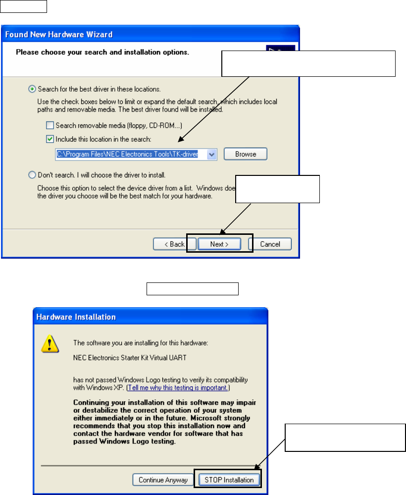
3. Select "Search for the best driver in these locations.” , check "Include this location in
the search:", and then click "Browse..." to select the driver directory path. The path
should be "C:¥Program Files¥NEC Electronics Tools¥TK-driver" as default installation.
If the installation directory is not default, then select "TK-driver" under the installation
directory.
Click Next > .
4. If the following dialog is opened, click Continue Anyway .
Click "Next"
Click "Continue Anyway"
Select the driver directory
- 25 -
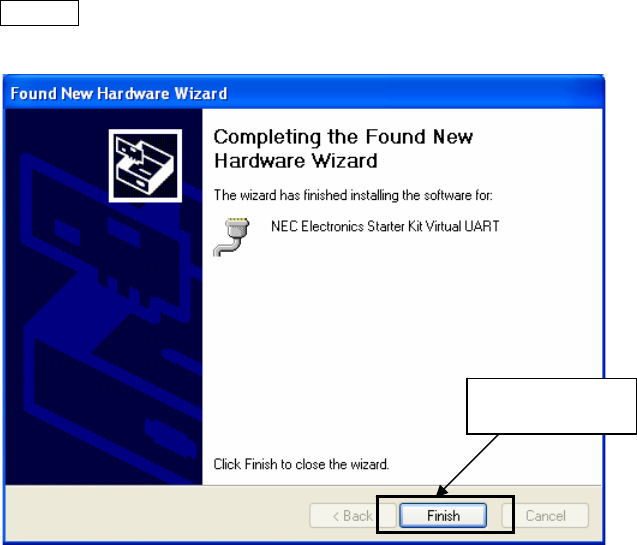
5. The installation of "NEC Electronics Starter Kit Virtual UART" driver is completed.
Click Finish .
6. Go to "1.3.3 Completion of the installation".
Click "Finish"
- 26 -
2.3.2 Install to Windows2000
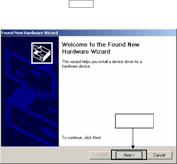
1. Once the TK-RF8058+SB is connected with USB, the "Found New Hardware Wizard" will
be started.
Select "No, not this time" and click Next > .
Click
- 27 -
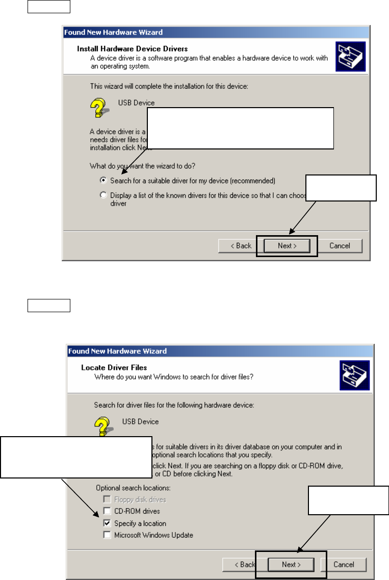
2. Select "Search for a suitable driver for my device".
Click Next > .
3. Select "Specify a location".
Click Next > .
Click "Next"
Select "Search for a suitable driver for my
device"
Click "Next"
Select "Specify a location"
- 28 -
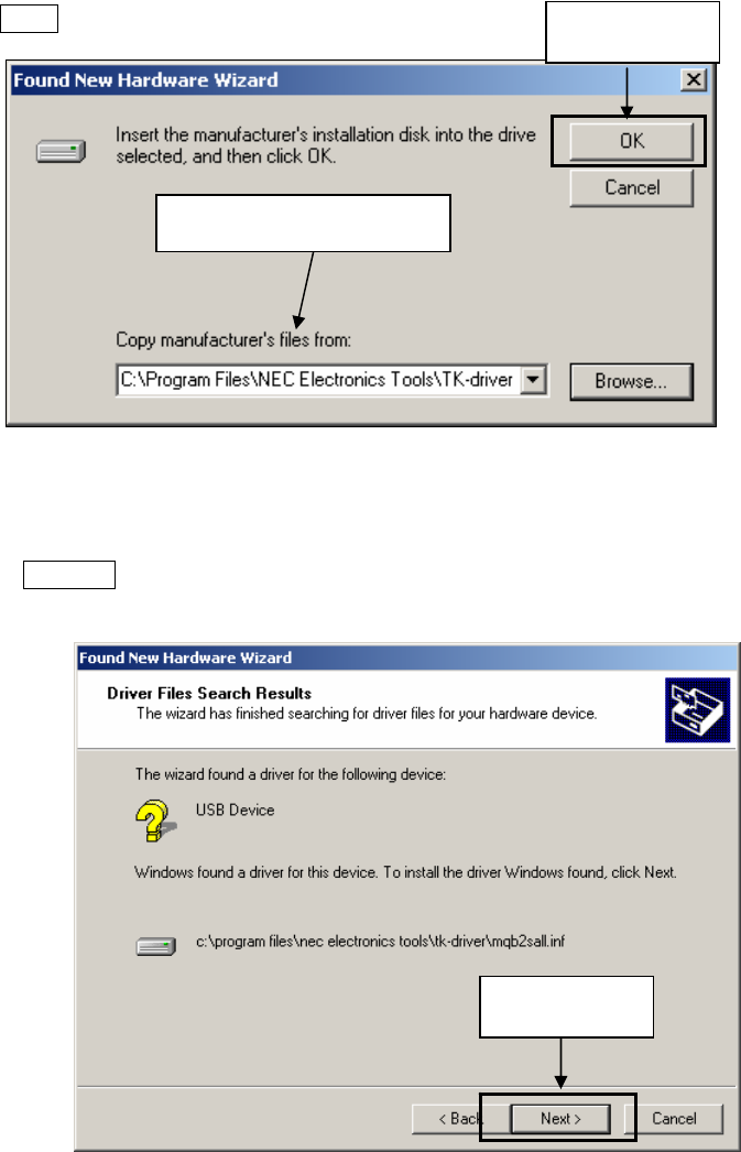
4. Select the driver directory path. The path should be "C:¥Program Files¥NEC
Electronics Tools¥TK-driver" as default installation.
If the installation directory is not default, then select "TK-driver" under the installation
directory.
Click OK .
5. Click Next > .
Click "Next"
Click "OK"
Select the driver directory
- 29 -
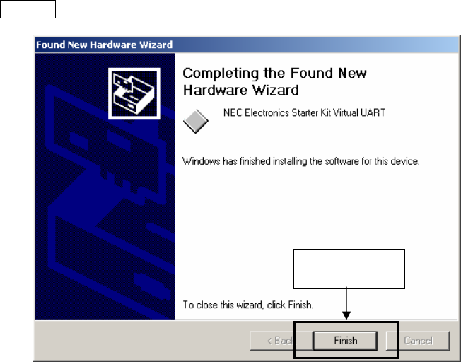
6. The installation of "NEC Electronics Starter Kit Virtual UART" driver is completed.
Click Finish .
7. Go to "1.3.3 Confirmation of the installation".
Click
- 30 -
2.3.3 Confirmation of the installation
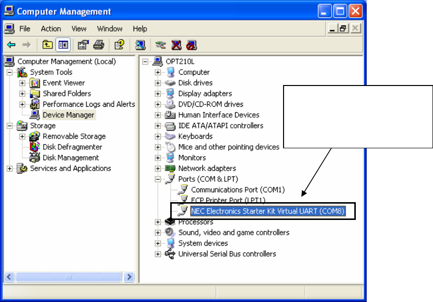
Please confirm “NEC Electronics Starter Kit Virtual UART(COMx)” in the device
manager of system in the control panel of the MS Windows.
Device Manager
The screen above shows that the COM port number is "COM8". If ID78K0R-QB is
not in use, you can use this port number for connecting TK-RF8058+SB.
When you change the USB port connection, the COM port number will be
changed as well.
Select this COM port number when you use WriteEZ5.
CAUTION
・Do not do “Hardware Modification Scan” when you communicate with the target device.
It is confirmed that “NEC
Electronics Starter Kit Virtual
UART(COMx)” exists.

- 31 -
2.4 Sample Environment
This section explains the overview and preparation of sample programs.
You need to install the sample programs on your system first before using them.
How to install the sample programs and where they should be intalled on your
system will be explained.
- 32 -
2.4.1 Installation of the sample programs
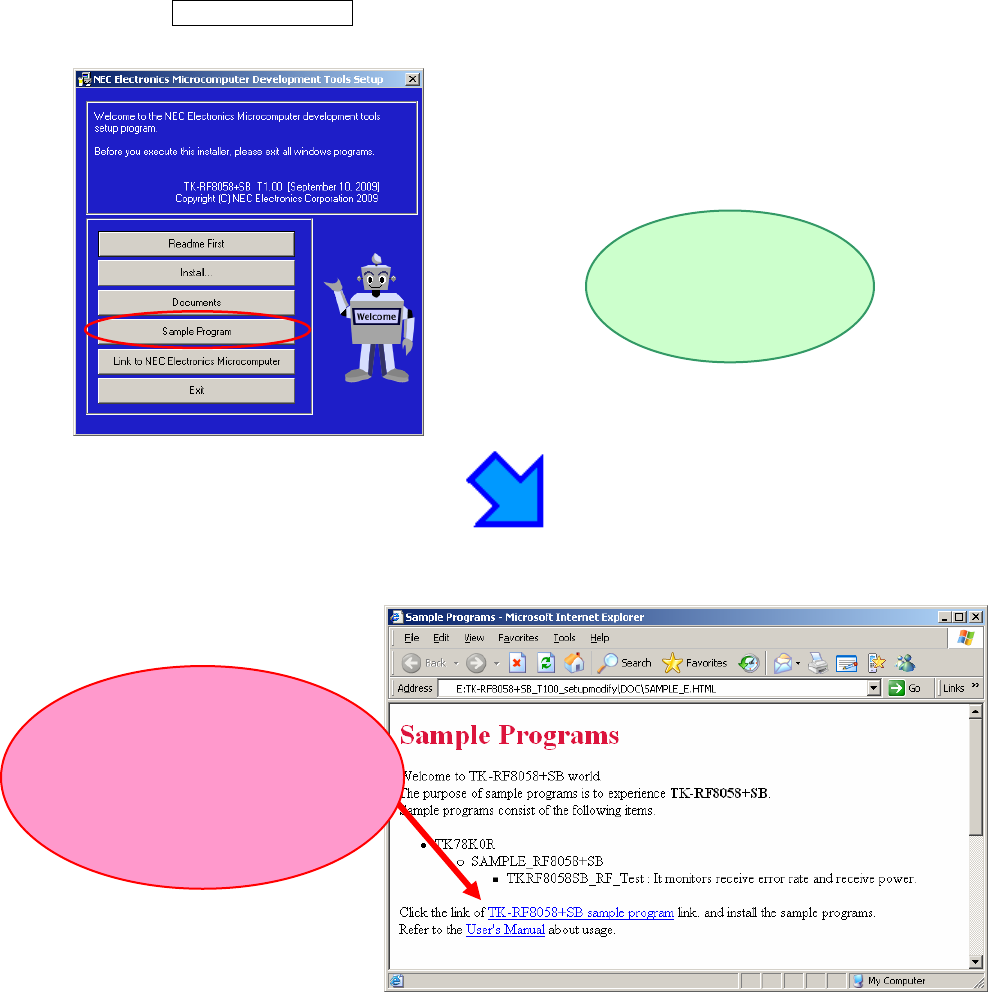
Insert the CD-ROM disk in the CD-ROM drive of your PC. The [NEC Electronics
Microprocessor Development Tools Setup] screen automatically appears.(if this screen does
not appear automatically, start setup.exe from Explorer. etc.)
Press the Sample Program button to start the WWW browser, and then click the
[TK-RF8058+SB Sample Programs] link.
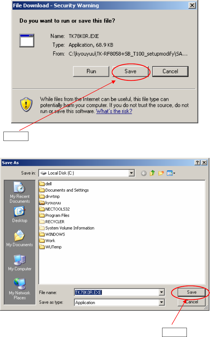
When[TK-RF8058+SB Sample Programs] is clicked, the following download
confimation window appears.
The WWW browser
starts up.
Click the [TK-RF8058+SB Sample
programs] link you can also
download the [User's Manual]
- 33 -
Click the Save butten.
After specifying the download destination folder,click the Save button.
The self-extraction sample program (TK78K0R.exe) is copied to the specified
folder.
The folder that the “TK78K0R” folder is made when this file is executed, and the
sample program is stored under the” TK78K0R” folder.

- 34 -
2.4.2 File Configuration of the sample program
The sample programs ware the following folders.
TK78K0R
SAMPLE_RF8058+SB
TKRF8058SB_RF_Test The sample program used in chapter 3.
The packet error rate and received signal

- 35 -
3 Experiences
Now you are ready to experience the operation of the TK-RF8058+SB using the
integrated development environment, PM +.
As a program for the TK-RF8058+SB, the RF test program (RF_Test) which you
installed in "2.4.1Installation of the sample programs" is used.
Later in this chapter, you will learn how to generate an executable file, how to
download it to the Flash, and how to execute the program.
You can understand the basic operation of the development tools (PM+,
ID78K0R-QB) and the basics of the project files that you need when you develop
application programs.
- 36 -
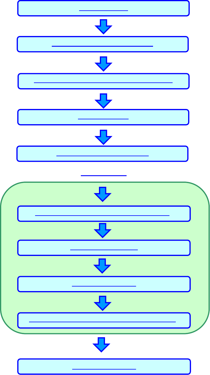
The overall flow is as follows.
Starting integrated debugger (ID78K0R-QB)
Executing program
Stopping program
Operation
Terminating integrated debugger (ID78K0R-QB)
Loading workspace (project)
Creating execution format
Reviewing Linker, Compiler option, Debug setting
TK board setting
Starting PM +
Terminating PM +
- 37 -
3.1 Starting PM +
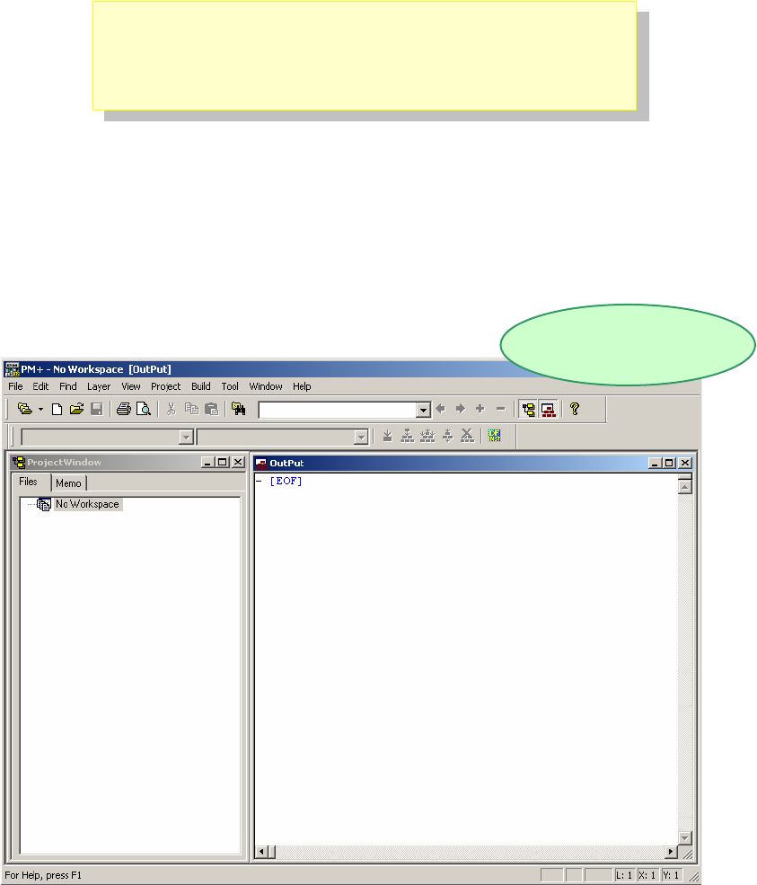
In the Windows Start menu, select [Programs]->[NEC Electronics Tools]->[PM +
V6.31]
PM + start up
- 38 -
3.2 Introduction to PM +
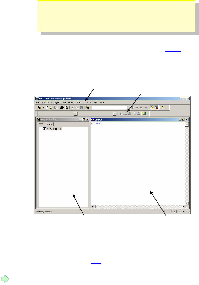
In PM +, application programs and environment setting are handled as a single Project, and series of actions
such as program creation using the editor, source management, build, and debugging are managed.
Also, one of more project files is managed together as a workspace.
Project window A window in which project names, source files, and include file are displayed using a
tree structure.
Output window A window in which the build execution status is displayed.
For details regarding menu bars and tool bars, refer to the PM + User’s Manual.
Project window Output window
Tool bar
Menu bar

- 39 -
What is a project?
A project is the unit in which PM + executes management, and refers to an application system
and environment development based on PM +.
PM + complies project information and saves it in a “project file”, from which it is then referenced.
What is a project file?
A project file is a file to which information such as the source file to be used in the project, the
device name, the tool options for complying, and the editor and debugger to be used have been
saved as “project information”.
The file name format is “ΔΔΔΔprj”.
Project files are created in folders that are set when creating new workspaces.
What is a project group?
A project group is a group comprised of a number of projects in an application system.
The target devices of each project that can be registered to one project group must be the
same.
What is a workspace?
A workspace is the unit used to manage all the projects or project group required for one
application system.
The file name of multiple project files is saved to a workspace file for referencing.
The file name format is “ΔΔΔΔprw”.
- 40 -
3.3 Loading Workspace (Project)
In this section, you will use the workspace that you created in "2.4Sample Environment"
For creating a new workspace, refer to "6.1Create a new workspace".
The workspace has information about the build environment for the sample programs.
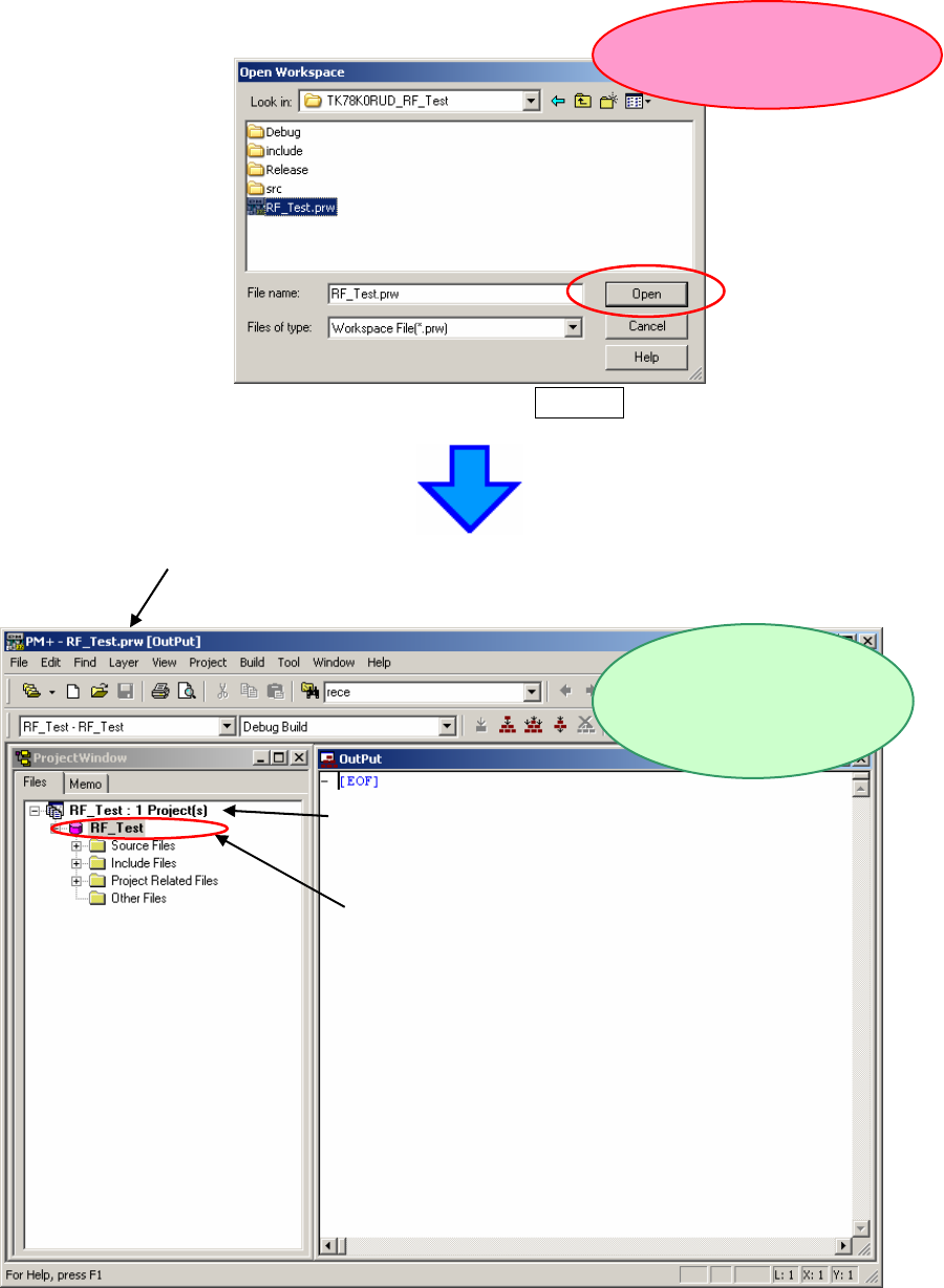
Select "File" on menu bar and "Open Workspace…".
Then, select “C:¥TK78K0R¥SAMPLE_RF8058+SB¥TKRF8058SB_RF_Test¥RF_Test.prw” .
- 41 -
“RF_Test.prw”and then press the Open button.
Open the folder in which the
sample program is located.
Workspace file name :RF_Test.prw
Project group
Project
The “RF_Test.prw” workspace
file is read
- 42 -
3.4 Configuration of Linker Option
The linker options have been set by the project file. However, some option settings will be
covered in this section because the linker option settings are important for debugging.
Following three settings are covered specifically.
- Outputs from debugging
- On-chip debug (bytes, security ID)
- Watchdog timer
Select "Tools" on menu bar, then "Linker options".
3.4.1 "Output1" Tab
Select "Output1" tab on "Linker Options" window, and see following settings.
- 43 -
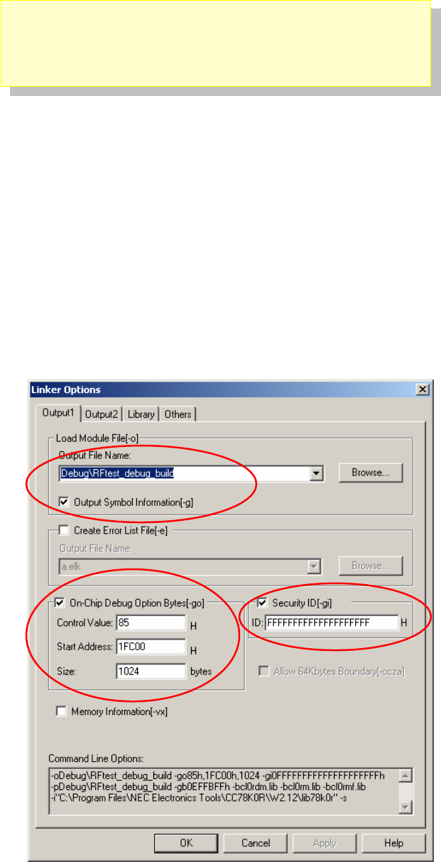
- Load Module File settings
Check "Output Symbol Information".
This enables to do source level debugging (setting break points, monitoring variables in
watch window, etc).
Also, you can specify the load module file name.
- On-Chip Debug Option Byte
Check "On-Chip Debug Option Byte". Enter "85" in "Control value". This setting enables
the on-chip debugging function of the microcontroller.
*For details of "Control value", refer to the user's manual of 78K0R/KG3 (U17894E).
See "Start address" is set to "1FC00", and "Size" is set to "1024".
These settings reserve the memory address area for the monitor program (the flash
memory area that the debugger uses for on-chip debugging).
In this case, the "Control value" is allocated to the address of C3H in flash memory, and
FFH is set to the next address. Because of this, the following areas could not be set the
segments.
<Address area that reserved by on-chip debugging>
- 2H, 3H
- CEH-D7H
- From the address set in "Start address" to the byte set in "Size"
- Security ID
Check "Security ID", and enter the security ID which is a unique ID code (10 bytes) to
authenticate when the debugger is launched.
The security ID is stored in the flash memory (C4H-CDH), and checked if it is the same
as the code entered in Linker options dialog when the debugger is launched.
The debugger will not be launched when the security ID is unmatched. By using this
function, you can secure the programs from leaks.
If you do not need to set the security, it is recommended to set the security ID
"FFFFFFFFFFFFFFFFFFFF" as this is the initial code.
If you forget about the security ID (stored in the address of C4H-CDH) or if you set wrong
on-chip debug option byte, you will not be able to use the debugger (ID78K0R-QB).
In this case, you need to use "WriteEZ5" to erase the built-in flash memory. By erasing
the flash memory, the security ID is set to "FFFFFFFFFFFFFFFFFFFF".
For details, refer to "6.4Erase of flash memory".
- 44 -
3.4.2 "Output2" Tab
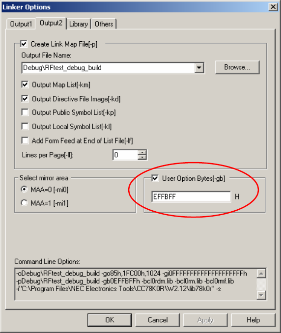
Select "Output2" tab on "Linker Options" window, and see following settings.
- User Option Byte
Check "User Option Byte", and then enter "EFFBFF". Here, you can do the
setting of watchdog timer, low-voltage detector, and system reserved
memory area. The 3 bytes you entered are stored at C0H-C2H on flash
memory:
- C0H: setting for watchdog timer
- C1H: setting for low-voltage detector
- C2H: setting for system reserved memory area (must be set as FFH)
This time, you disabled the watchdog timer and the default start function of
low-voltage detector.
For details, refer to the user's manual for uPD78F8058.
- 45 -
3.5 Configuration of Compiler Option
The compiler options have been set by project file. However, because some
compiler options are useful, following two settings are covered specifically in this
section.
- Enable C++ comments
- Use multiplier and divider
Select "Tools" on menu bar, then "Compiler options".
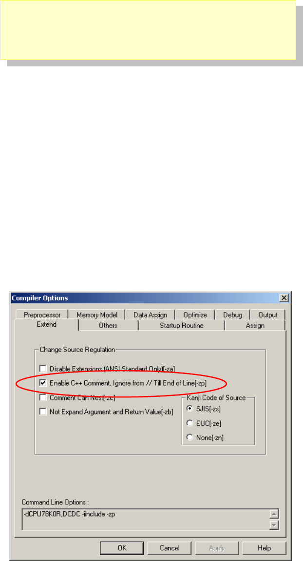
3.5.1 "Extend" Tab
Select "Extend" tab, and check "Enable C++ Comment".
This setting allow you to use the C++ comment using "//".
It is useful feature when developing code.
- 46 -
3.5.2 "Startup Routine" Tab
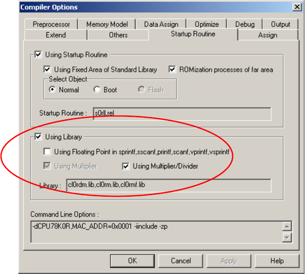
Select "Startup Routine" tab, and check "Using Library" and "Using
Multiplier/Divider". The Microcontroller has feature of multiplier/divider to increase
those calculation speed.
- 47 -
3.6 Configuration of Debugger setting
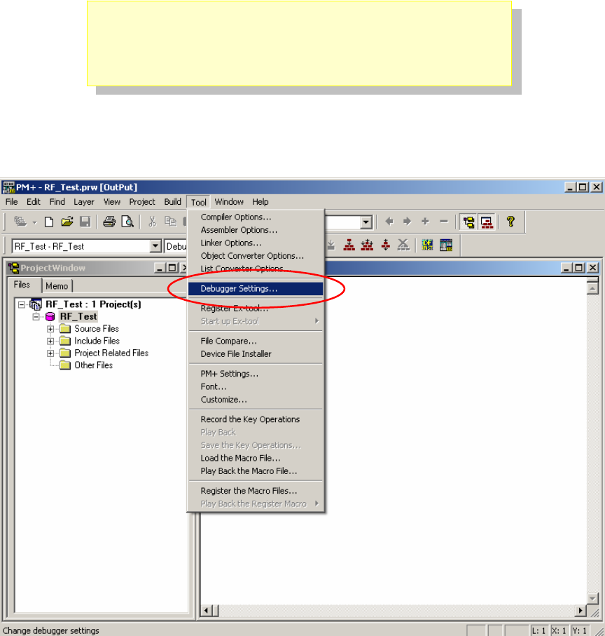
Please Choose [Tool] -> [Debugger Setting] at the pull-down menu.
- 48 -
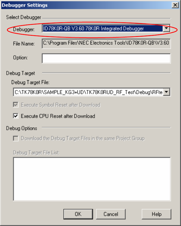
Check if "ID78K0R-QB V3.60 78K0R Integrated Debugger" is selected on
"Debugger".
- 49 -
3.7 TK board setting
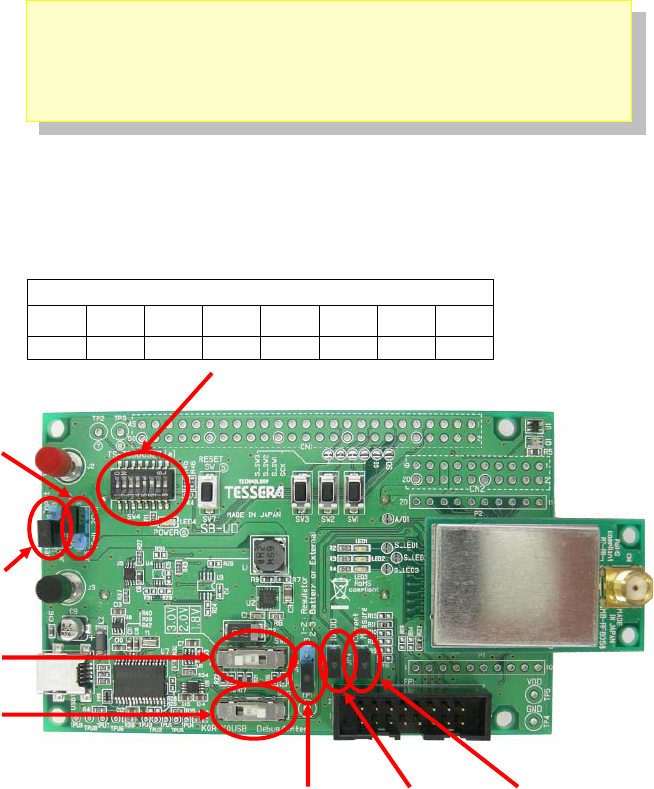
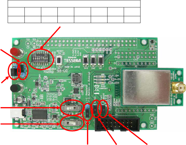
Please set the switches on the TK-RF8058+SB board as follows.
After the switch settings are completed, connect the PC to USB1 on
TK-RF8058+SB with USB cable.If the "Found New Hardware Wizard" is started,
install USB driver with referring "2.3USB Driver".
SW4 setting
1 2 3 4 5 6 7 8
ON ON ON ON ON ON OFF OFF
JP5:Any
JP3:
1-2short(USB)
SW5:3.0V
SW6:
「Debug/Writer」
JP2:
1-2short(Regulator)
JP1:short JP4:short
- 50 -
3.8 Creating execution format
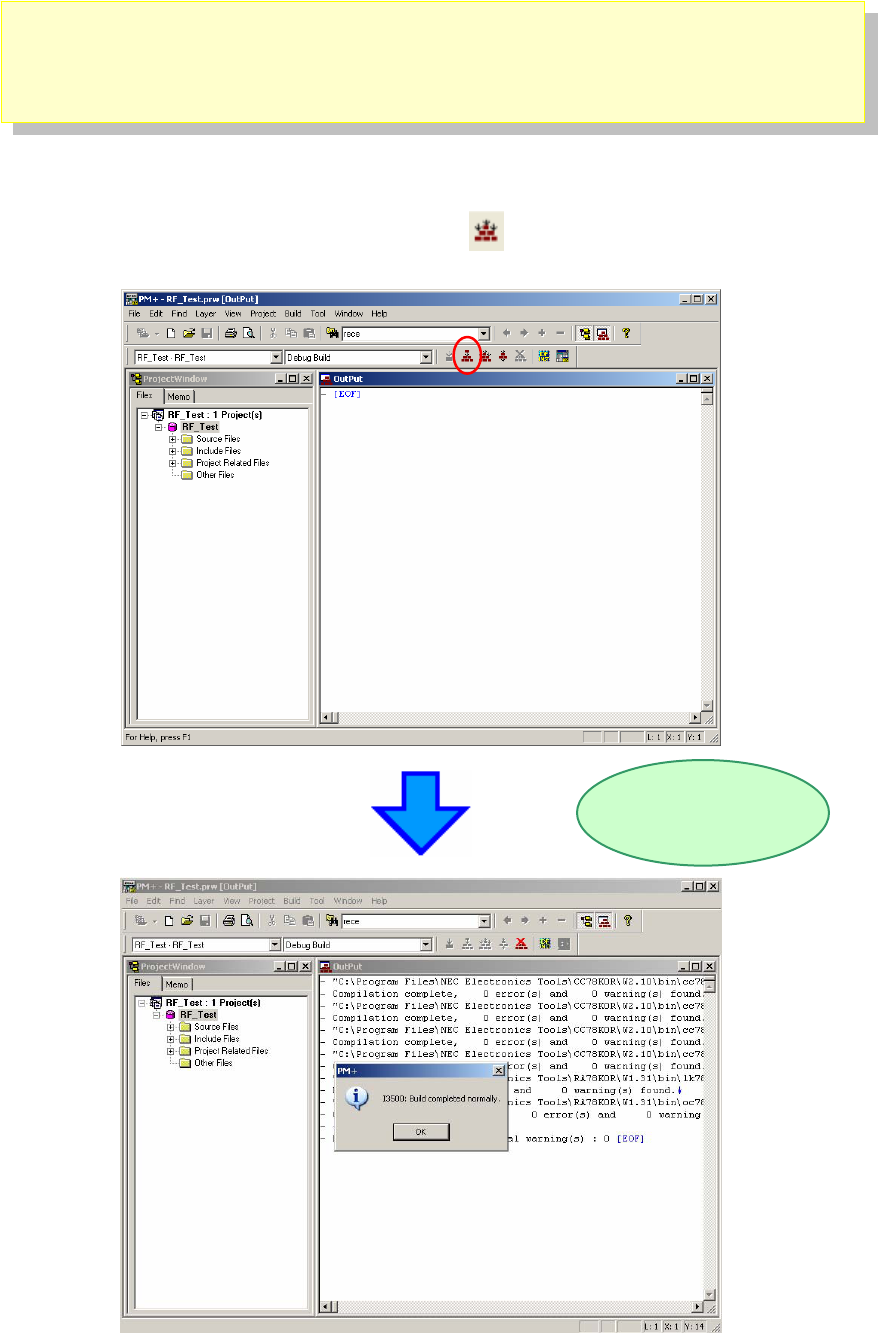
Please go back to PM +.
Please re-compile the project by clicking the button at the menu bar.
Build has been completed successfully.
Build process is
executed

- 51 -
What is build ?
Build is a function that creates an executable file, etc., from a source file registered to a project.
PM + automatically performs compiling, linking, and other processing actions.
On the second and subsequent build, PM + also automatically delects files that have been updated
from the previous build processing, and complies and assembles only the relevant files, thereby reading
the time required for build processing.
What is rebuild ?
Build compiles and assembles only the source files that have been updated since the previous
time, whereas rebuild compiles and assembles all the source files.
When setting, such as compiler options, have been changed, not build, but rebuild, must be
Selected.
- 52 -
3.9 Starting integrated debugger (ID78K0R-QB)
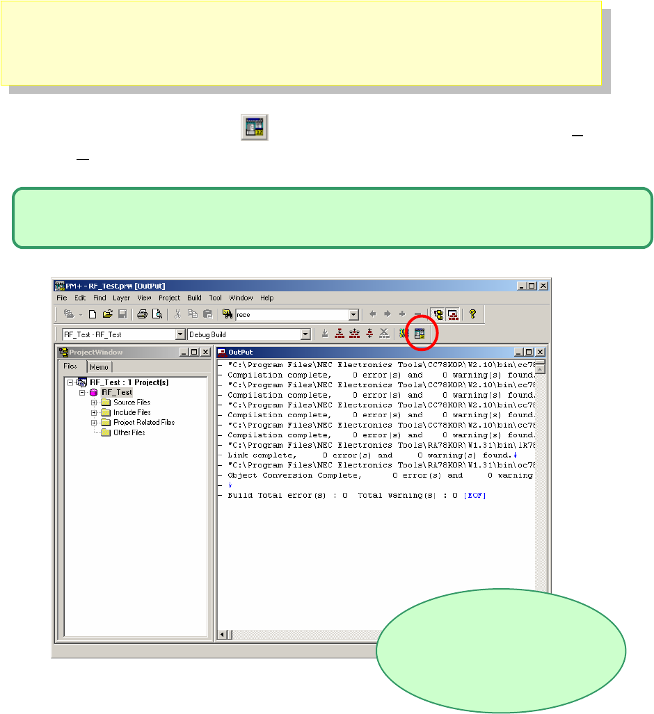
Please select the Debug button ,of PM +, or in the menu, select [Build(B)]
→[Debug(D)].
If the debug button is not displayed, in the menu, select [Tool]→[Debugger
Setting...]“ID78K0R-QB V3.60 78K0R Integrated Debugger”
ID78K0R-QB is launched
- 53 -
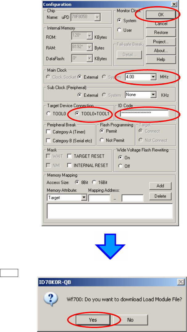
Then, you will see the Configuration dialog.
Please choose “Tool0+Tool1” in the "Target Device Connection", and choose
"4.00MHz" in the "Main Clock", then, please input 20 Fs,
0xFFFFFFFFFFFFFFFFFFFF, in the ID Code.
Then, please click “OK”.
Click Yes when the confirmation dialog for downloading load module file is opened.
- 54 -
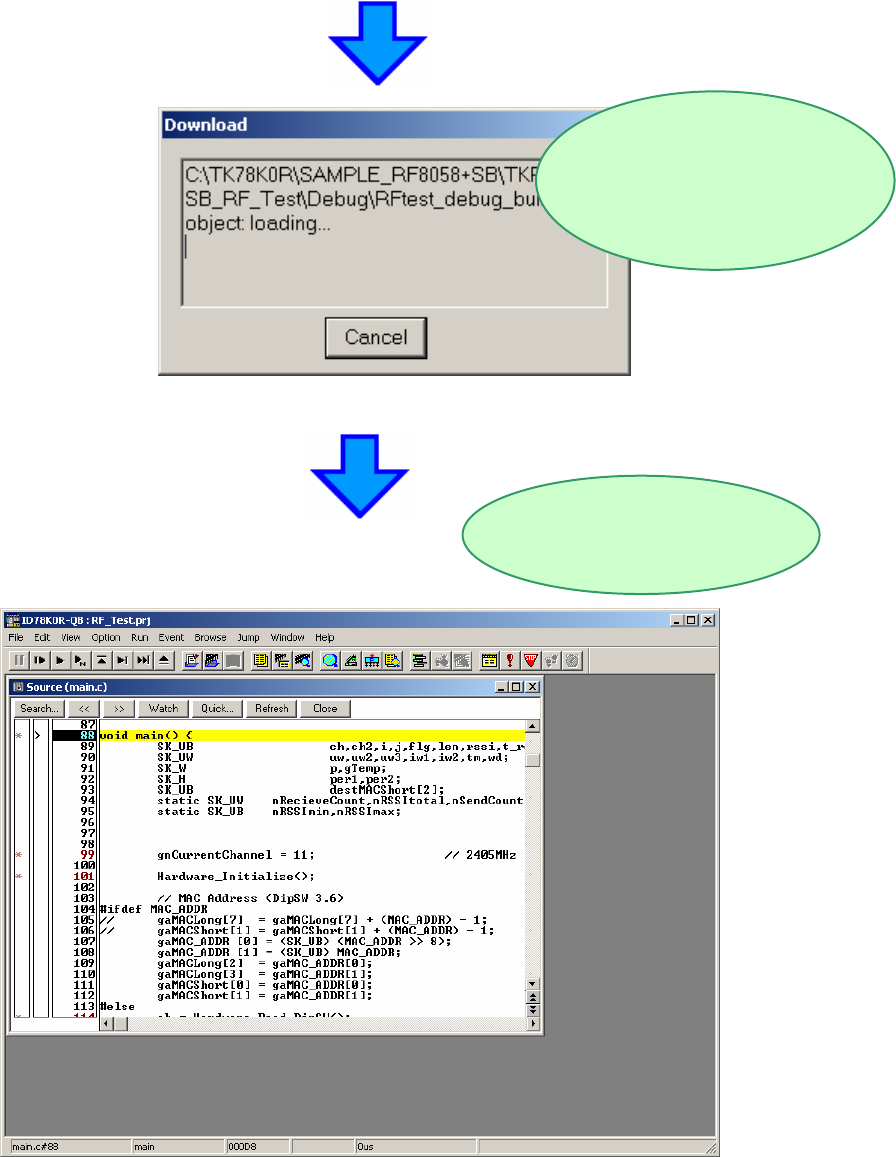
NOTE:
Completion of the download does not mean running the programs. To run the sample
programs, go to "3.11 Executing program".
ID78K0R-QB starts and downloading
the program to flash memory.
When the download is
completed, the source
code will be dis
p
la
y
ed
- 55 -
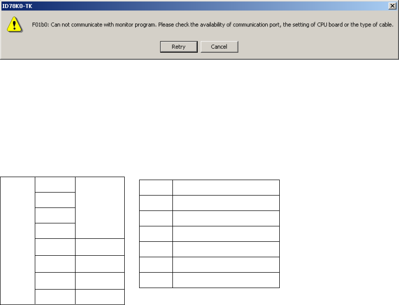
Normally, if communication with the CPU fails, the following error messages are
output.
If you observe the message please confirm the following items.
1. Please confirm the switch on the board is set as follows.
2. Please confirm the power LED4 is lighted.
After checking the above items, start ID78K0R-QB again.
Bit1
Bit2
Bit3
Bit4
ALL ON
Bit5 ON
Bit6 ON
Bit7 OFF
SW4
Bit8 OFF
SW6 「Debug/Writer」
SW5 3.0V
JP3 1-2short(USB)
JP5 Any
JP2 1-2 short (Regulator)
JP1 Short
JP4 Short
- 56 -
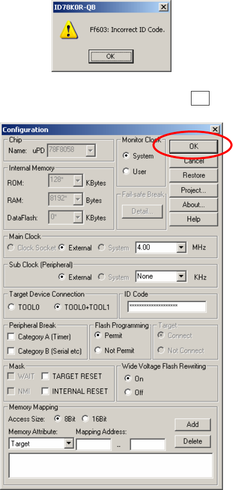
If the ID code is wrong, you may find the following messages on the display.
The following "Configuration" screen is displayed when OK is pushed and input a
correct ID code, please.
The default setting of the ID code is ”0xFFFFFFFFFFFFFFFFFFFF”. You can set
an alternative ID code on the linker option tab.
If the setting of On-Chip Debug Option Byte is "Does not erase data of flash
memory in case of failures in enabling on-chip debugging" and if you forget the
security ID, you need to erase the flash memory completely.
To erase the flash memory, please refer to the section 6.4, “Erasing the Flash
Memory”.
- 57 -
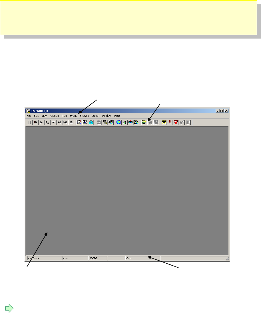
3.10 Introduction of the integrated debugger (ID78K0R-QB)
ID78K0R-QB displays the internal status of the CPU and controls monitor
functions in the main window.
The initial screen of ID78K0R-QB is as follows.
< Main window>
For more details, please refer to the user’s manuals of ID78K0R-QB.
Status bar
Menu bar
Window display area
Tool bar
- 58 -
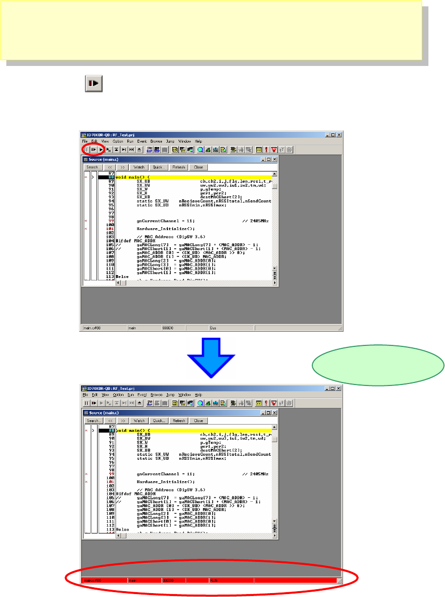
3.11 Executing a program
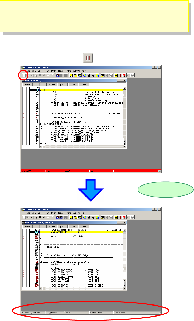
If you click “GO” , the execution of the code will start.
You can know it by the red bar at the bottom.
While a program is running, the status bar will be red.
Execute the program
- 59 -
3.12 Stop a program
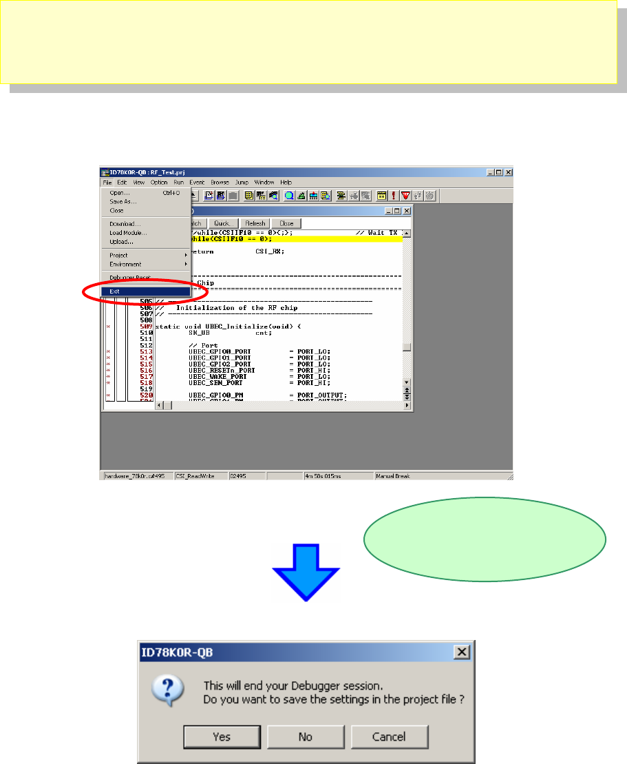
Now, you are going to stop the program.
Press the ID78K0R-QB’s stop button , or in the menu, select [Run]→[Stop].
When the program stops, the status bar changes back to the original color.
Stop the program
- 60 -
3.13 Terminating integrated debugger (ID78K0R-QB)
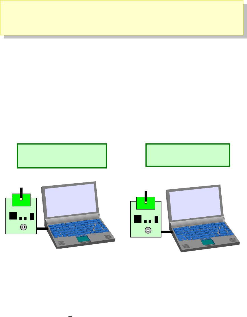
Select "File" on menu bar, then "Exit".
If you push the “Yes”, ID78K0R-QB is terminated after preserving a present
environment.
If you push the “No”, ID78K0R-QB is terminated without preserving a present
environment.
The Exit confirmation dialog box is
displayed.
- 61 -
3.14 The RF Test Program
3.14.1 Procedure for one to one transmit/receive test
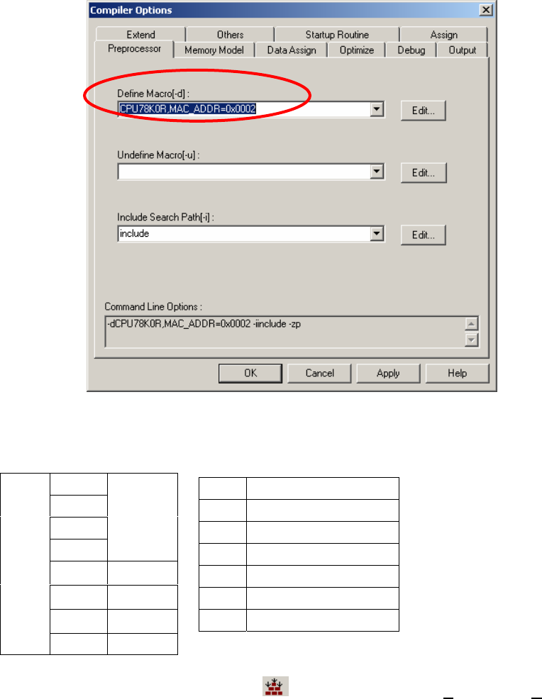
Assumption here in this section is, you have two TK-RF8058+SB boards, in one of which the
execution code for the “RF_TEST” was programmed by the debugger. You also prepare two
PCs or one PC with more than one usb interface.
We will use the board you have downloaded the executable program with the short address
0x0001 as a transmitter. We now learn how to prepare an executable program for receiver
side, which may be assigned a short address of 0x0002.
Settings for a receiver
1). Please start-up the PM+ from the
“C:/TK78K0R/SAMPLE_RF8058+SB/TKRF8058SB_RF_Test/RF_Test.prw”
2). Please choose [Tool(T)] → [Compiler Options] Æ [Preprocessor]
Receiver
Short address : 0002
Transmitter
Short address : 0001
- 62 -
3). Please alter the Macro Definition from “CPU78K0R,MAC_ADDR=0x0001” to
“CPU78K0R,MAC_ADDR=0x0002”.
4). Now, you set the short address of the receiver at 0x0002.
5). Please set the switches on the receiver as follows,
6). Then, please rebuild it by pushing the button, or select [Biild(B)]→[rebuild(R)].
7). You will follow the instructions in the chapter 3.9.
8). If you complete the download of the load module file, please close the debugger.
9). Then, please remove the USB cable.
Bit1
Bit2
Bit3
Bit4
ALL ON
Bit5 ON
Bit6 ON
Bit7 OFF
SW4
Bit8 OFF
SW6 Debug/Writer
SW5 3.0V
JP3 1-2short (USB)
JP5 Any
JP2 1-2 short (Regulator)
JP1 Short
JP4 Short

- 63 -
10). Then, the board setting is configured as follows as a receiver.
11). Connect the board with a PC by a USB cable, then you will find the Power LED lit on the
board.
Bit1
Bit2
Bit3
Bit4
ALL
OFF
Bit5 ON
Bit6 ON
Bit7 OFF
SW4
Bit8 OFF
SW6 「K0R-K0USB」
SW5 3.0V
JP3 1-2 Short(USB)
JP5 Any
JP2 1-2 Short (Regulator)
JP1 Short
JP4 Short

- 64 -
12). Then, we need a hyperterminal on the PC.
13). On MS-Windows in your PC, please select [All Programs] -> [Accessory] ->
[Communication] -> [HyperTerminal]
14). You may assign your favorite name on a connection. Then, click OK.
15). You need to learn the COM port number you connected the USB cable. If you
don’t know the com port number, please find it at [Control Panel] Æ [System]
Æ [Hardware] Æ [Device Manager] Æ [Port (COM and LPT)].
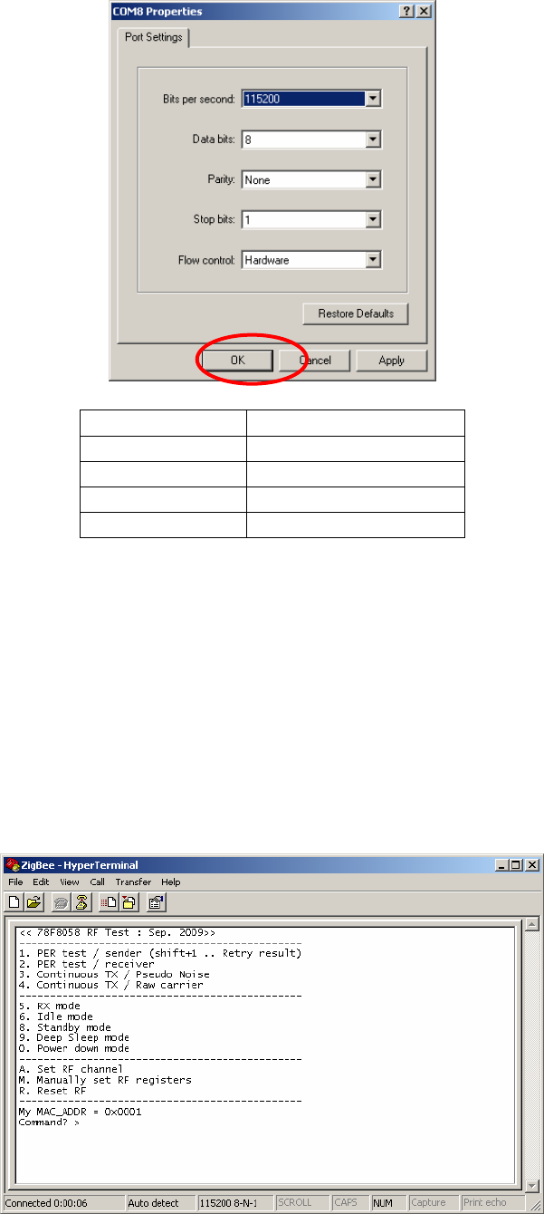
- 65 -
(Property -> Setting -> ASCII)
Local Echo OFF
No Line Feed
16). Please set the COM port at 115200 bps, 8 data bits, no parity, 1 stop bit, and
no flow control.
Then, please click “OK”.
17). Then, please reset the receiver board by pressing the SW7.
18). Now you will find the following opening menu in the window.
Bits per second 115200
Data bits 8
Parity None
Stop bits 1
Flow control None

- 66 -
19). Please select “2” from the MENU to start the board as a receiver.
20). If you see the display as shown above, the receiver set-up has been
completed.
Command? >2 (PER test/reciever)
[My Profile]
-------------------------------------
MAC : 22:95:00:02:00:00:00:47
Short : 0002
PanID : 2514
-------------------------------------
[Set channel to 11 (Cmd)]
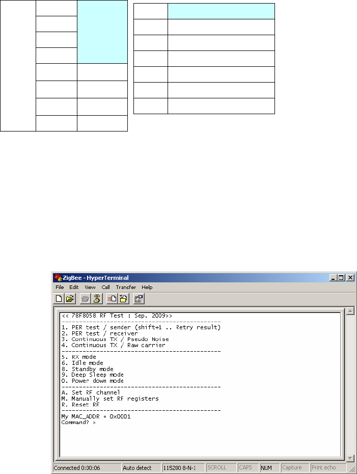
- 67 -
Settings for a transmitter
1). Please configure the board of a transmitter as follows,
2). Please connect the transmitter board to a PC. Please confirm the LED lit on
the board.
3). Please start-up a hyperterminal for a transmitter.
4). Please reset the transmitter board by pressing the SW7.
5). Now you will find the following opening menu in the window.
Bit1
Bit2
Bit3
Bit4
ALL
OFF
Bit5 ON
Bit6 ON
Bit7 OFF
SW4
Bit8 OFF
SW6 「K0R-K0USB」
SW5 3.0V
JP3 1-2 short(USB)
JP5 Any
JP2 1-2 short(Regulator)
JP1 Short
JP4 Short
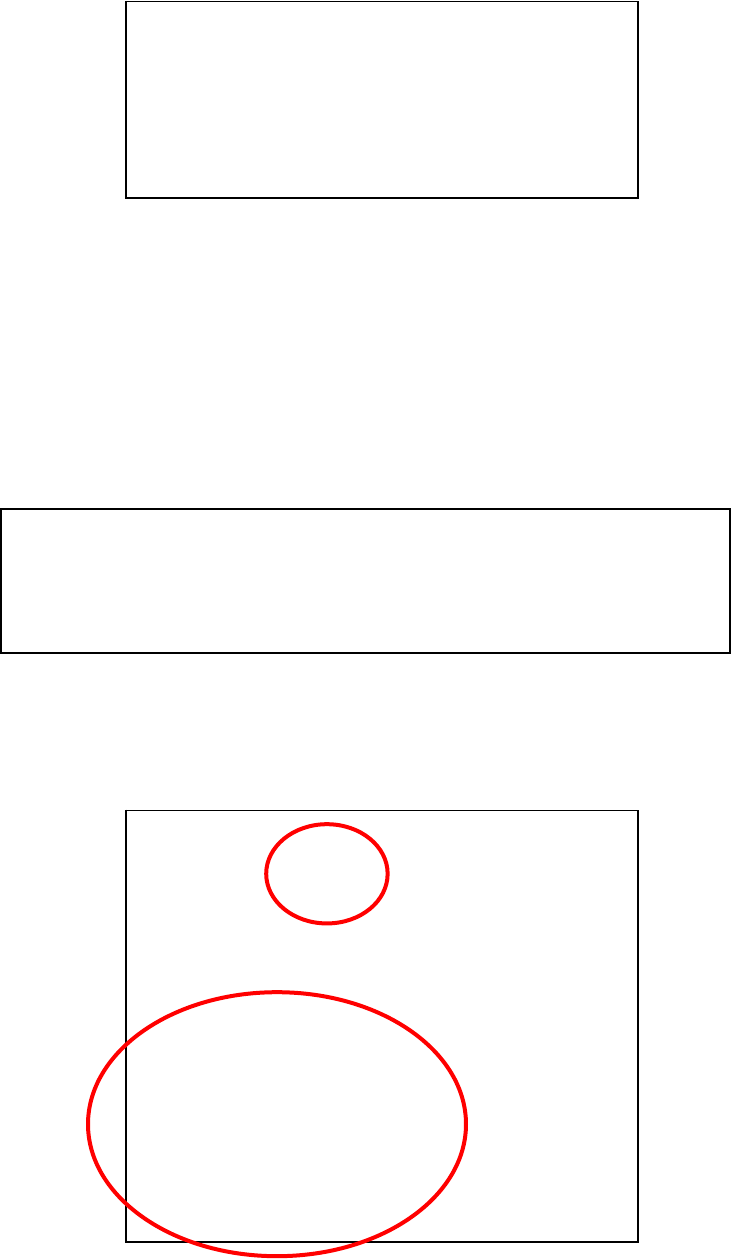
- 68 -
6). Please select the command “1” to start the Packet Error Rate test.
7). If you see “Send to (Short addr) ? :”, please input the receiver address of
0002.
8). Then, you will be asked how many packets you wish to consume in the PER
test.
9). You may input “1000”.
10). Then, you will be asked the interval of packets in msec.
11). You may input 3 msec.
12). Then, the PER test will be executed.
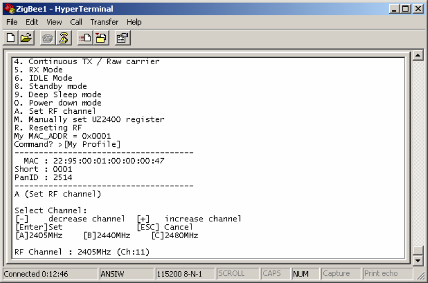
13). You will see,
Sent: The number of packets sent.
Received: The number of the received packets.
PER: The calculated PER in %.
RSSI: The maximum and minimum RSSI values in the PER test
[Note]
PER= Packet Error Rate
RSSI= Received Signal Strength Indication
-------------------------------------
Send to (Short addr) ? : 2
Send count (dec) ? : 1000
Interval (dec/msec) ? : 3
[Set channel to 11 (Cmd)]
Prepare to send..OK
[Set channel to 11 (Current)]
Request to result..OK
[Results]
-------------------------------------
From : 0001
To : 0002
-------------------------------------
Sent : 1000
Recieved : 1000
PER : 0.0000%
RSSI : max FF / min D0
-------------------------------------
Press any key to the menu
Command? >1 (PER test/sender)
[My Profile]
-------------------------------------
MAC : 22:95:00:01:00:00:00:47
Short : 0001
PanID : 2514
-------------------------------------
Send to (Short addr) ? :
- 69 -
21). Channel setting
In the previous example, you may have also found the RF channel used in this
test is the Channel 11. The channel is specified by the IEEE 802.15.4
specification.
The channel 11 is assigned at 2405 MHz. You can change the channel in the PER
test in 5MHz step to the maximum channel of 26th at 2480 MHz.
To do it, please press “A” in the command prompt. Then, please choose the
channel by [+], [-], [A], [B], or [C]. In the example below, the channel 23th, 2465
MHz, was selected.

- 70 -
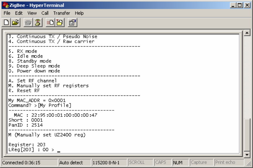
To execute the PER test at the channel 23, press [Enter] in your keyboard, then,
choose “1” to initiate the PER test mode. Then, you may input 1000 packet in 5
msec interval to see the following example. Please confirm the channel used is
23th in the display. Please note the receiver will learn which channel is to be used
for the test automatically.
[My Profile]
-------------------------------------
MAC : 22:95:78:01:00:00:00:47
Short : 0001
PanID : 2514
-------------------------------------
Send to (Short addr) ? : 02
Send count (dec) ? : 1000
Interval (dec/msec) ? : 5
[Set channel to 11 (Cmd)]
Prepare to send..OK
[Set channel to 23 (Current)]
Send.. 0
Request to result..OK
[Results]
-------------------------------------
From : 0001
To : 0002
-------------------------------------
Sent : 1000
Recieved : 1000
PER : 0.0000%
RSSI : max FF / min FF
-------------------------------------
- 71 -
22). Adjusting the output power
You may wish to control the output power in the PER test.
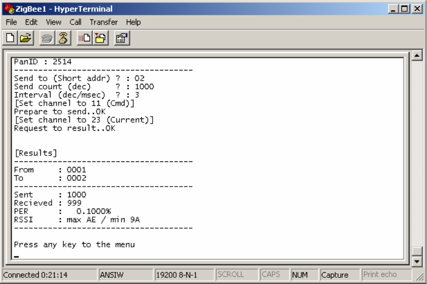
For it, please select “M” in the menu.
You will be asked the register ID. Please input “203”.
Then you will see, “LREG[203] : 00 >1F”.
It means the current value at the register [203] is 0x00, which means 0 dB.
0x00 is the reset default.
The register bits are defined as follows,
LREG[203]: [7:3] -> small scale tuning
000000: 0 dB
000001: -0.1dB
|
111111: -8.30 dB
For instance, if you wish -8 dB, please input “1F”, as follows,
“LREG[203] : 00 > 1F”
Then, you will start the PER test.
- 72 -
You may find larger PER value with smaller RSSI value in this case.
Please note this adjustment is applied only to the transmitter. The receiver always
sends back the test results with the 0 dB output power using the channel 11th.
- 73 -
3.14.2 PER test / receiver
The Menu 2 sets the board to the receiver in the PER test.
If you have two PCs, you can connect two boards to each of two PCs, then,
you will apply this mode to one of them.
3.14.3 Continuous TX / Pseudo Noise
The Menu 3 initiates the modulated RF transmission. The data carried are
pseudo random numbers. You can define the channel using the menu 9,
and the output power using the menu 0.
3.14.4 Continuous TX / Raw carrier
The Menu 4 initiates the carrier transmission. The output power is not 0 dB
as a reset default. You can define the channel using the menu 9.
3.14.5 RX Mode
The Menu 5 initiates the receiver mode.
3.14.6 IDLE MODE
The Menu 6 sets the UZ2400 into the IDLE mode.
3.14.7 Standby MODE
The Menu 8 sets the UZ2400 into the Standby mode.
3.14.8 Deep Sleep mode
The Menu 9 sets the UZ2400 into the Deep Sleep mode.
3.14.9 Power down mode
The Menu 0 sets the UZ2400 into the Power down mode.
- 74 -
3.14.10 Set RF channel
The Menu A allows you to set the RF channel.
3.14.11 Manually set UZ2400 register
The Menu M allows you to set the UZ2400 registers.
Please refer to the datasheet for the definition of registers.
3.14.12 Resetting RF
The Menu R allows you to reset the UZ2400 registers.
- 75 -
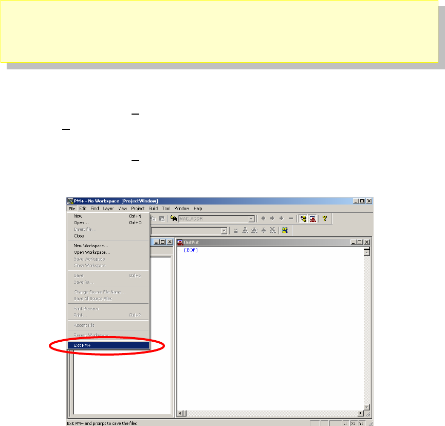
3.15 Terminating PM +
In the PM + menu, select [File]→[Save Workspace].
Then, select [File]→[Close Workspace].
In the PM + menu, select [File]→[Exit PM +].
PM + ends.

- 76 -
4 Hardware Specifications
In this chapter, the hardware of TK-RF8058+SB will be explained.
Microcontroller μPD78F8058
Clock
CPU main system clock:
20/8/1MHz (Internal oscillator)
16/8/4/2/1MHz (Generated from the
32MHz main clock)
CPU subsystem clock:32.768KHz
Interface
USB connector(MiniB)
Extension connector(CN1: not mounted)
External Power Supply Terminals
(J2,J3)
MINICUBE2 connector(FP1)
Power supply
voltage
USB Power: 5.0V
One AA battery: 1.5V
Two AA batteries: 3.0V
External Power Supply at J2 and J3: 1.8V
- 3.6V
Input/output for
operation check
use
・LED x3 : Only LED1 is connected to the
MB-RF8058 module.
・Push switch x3: Only SW1 is connected
・Dip switch (SW4)
・Reset switch (SW7)
・Temperature sensor (U1: not used)
・Illminance sensor (Q1: not used)
・7LED x3
Other hardware
・Power LED(LED4)
・Voltage regulation selection by SW5 to
3.0V, 2.0V, or 1.8V
- 77 -
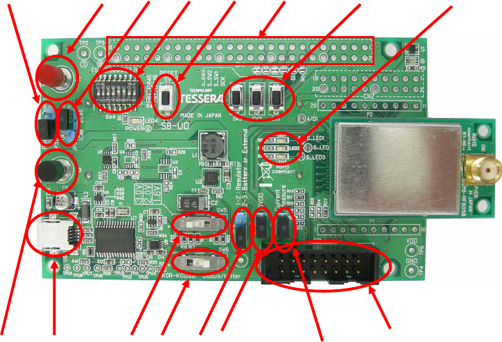
FP1
SW1, 2, 3
SW7SW4
JP5
J2
JP4
JP1
JP2
SW6 SW5 USB1 J3
JP3 LED1, 2, 3
JP4JP2
CN1
4.1 Layout of hardware functions
- 78 -
4.2 Hardware Functions
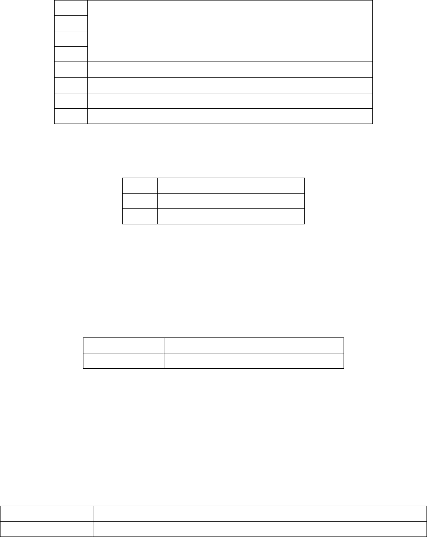
4.2.1 SW4 (Dip Switch)
Mode setting
1 bit
2 bit
3 bit
4 bit
ALL ON → USB TK debugger
ALL OFF → PC HyperTerminal mode
5 bit Pull-up for RESET terminal(ON)/ no pull-up (OFF)
6 bit Power LED ON/OFF
7 bit Not used (TP2)
8 bit Not used (TP3)
4.2.2 SW5
Selection of the regulator
1.8V 1.8V output to the module
2.0V 2.0V output to the module
3.0V 3.0V output to the module
Caution) Never alter the SW5 settings while a power source is being
applied.
The regulator chip may be destroyed.
Alter the SW5 settings after the SW3 jumper pin is removed.
4.2.3 SW6
Serial Communication Mode Setting
K0R-K0USB UART- USB for HyperTerminal
Debug/Writer For ID78K0R-QB or WriteEZ5
4.2.4 JP1
Power supply to peripheral circuits such as LEDs and the temp sensor.
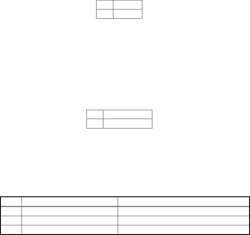
4.2.5 JP2
Selection of a power source
1-2 short-circuit Regulation output of 1.8V, 2.0V, or 3.0V
2-3 short-circuit No regulation from two batteries or the external power source
- 79 -
4.2.6 JP3
Selection of a power source to the regulator
1-2 USB
2-3 Battery
4.2.7 JP4
A jumper to measure a consumed current on the module.
If you don’t execute measurement, please keep short-circuited.
If you measure a consumed current to the module, please use external power
supply or two batteries for precision measurement.
4.2.8 JP5
A selection of one battery or two batteries.
1-2 One battery
2-3 Two batteries
4.2.9 SW1,SW2,SW3
SW3 and SW4 are tact switches. The port inputs are short-circuited to ground,
while they are being pushed, and kept open otherwise. Therefore please set the
on-chip pull-up registors(PU1) during initializing routine of your program code.
(For more detail, please refer to the User’s manual of the μPD 78F8058CPU.)
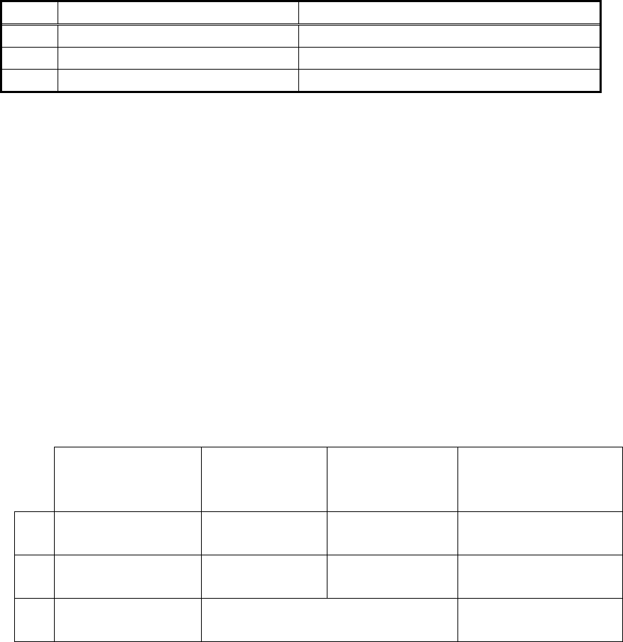
Connected MCU pin Note
SW1 P15/RTCDIV/RTCCL/GPIO2 GPIO2 belongs to the RF part
SW2 Not connected
SW3 Not Connected
4.2.10 SW7
SW7 is the reset switch. CPU can be reset by pushing.
- 80 -
4.2.11 LED4
LED4 indicates if power is being applied to the board, if SW4-5 is on.
If you want to save power by turning the LED4 off, please set SW4-5 to off.
4.2.12 LED1, LED2, and LED3
LED1, LED2, and LED3 are available for applications. To make an LED on,
please set the output port LOW.
Connection of LED1, LED2, and LED3
Connected MCU pin Note
LED1 P16/TI01/TO01/INTP5/GPIO3 GPIO2 belongs to the RF part
LED2 Not connected
LED3 Not connected
4.2.13 FP1
The connector for MINICUBE2.
Please set the side switches of MINICUBE2 to “M1” and “T”.
4.2.14 J2 and J3
J2 and J3 is a pair of terminals to input power supply from an external power
source. The accepted range of power source is from 1.8V to 3.6V.
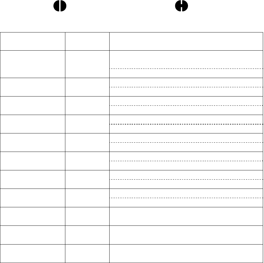
4.3 Summary of Power Supply Settings
Summary of power supply settings
USB Power
An external
source
At J2 and J3
Two batteries One battery
JP3 1-2 connected
(USB)
Any 1-2 connected
(USB)
2-3 connected (Battery)
JP5 Any 1-2 connected
(1Cell)
2-3 connected
(2Cells)
1-2 connected (1Cell)
JP2 1-2 connected
(Regulator)
2-3 connected (Battery or External) 1-2connected
(Regulator)
- 81 -
4.4 Solder-short pad
The solder-short pad offers a way to modify the circuit on the module.
The solder-short pad looks like the picture below.
To open it, please cut the narrow part by a knife. To connect them back, please
form a solder bridge on the pad.
Solder-short pad Solder-short pad
(Open) (Short)
Solder-short pad
name
Factory
default
Connection
Connection between
P16/TI01/TO01/INTP5/GPIO3 and LED1
S_LED1 Short
Connection to LED2
S_LED2 Short
No connection to the MB-RF8058 board.
Connection to LED3
S_LED3 Short
No connection to the MB-RF8058 board
Connection from SW1
S_SW1 Short
Connection from SW2
S_SW2 Short
No connection to the MB-RF8058 board
Connection from SW3
S_SW3 Short
No connection to the MB-RF8058 board
Analogue output from the temperature sensor
AD1 Short
No connection to the MB-RF8058 board
Analogue output from the illumination sensor
AD2 Short
No connection to the MB-RF8058 board
SCK Open Not used
SI Open Not used
SO Open Not used

- 82 -
5 Troubleshooting
This chapter describes how to solve troubles you may face.
5.1 If you cannot find USB driver when you connect PC to the kit
Check Point 1
If you use USB hub, do not use it. (USB hub is not supported)
Check Point 2
Check if you installed "Starter Kit USB Driver" in "1.2 Installation of Development
Tools". If not, install the driver.
Check Point 3
Check if the settings of the switch on the kit are correct with referring to "1.3
Installation of USB Driver".
Check Point 4
If above 3 check points are confirmed, disconnect the USB cable from PC and
re-connect again. It should show the "Found New Hardware Wizard" wizard. Operate
the installation with referring to "1.3 Installation of USB Driver". After the installation,
make sure you go through "1.3.3 Completion of USB Driver Installation" to confirm the
USB driver installation.
5.2 Error when you start the debugger
There could be several reasons to make errors happen.
The solving processes differ depending on errors. Please check the error message first.
The solving processes for each error are as follows.
- 83 -
5.2.1 "Can not communicate with Emulator..." (F0100 or A0109)
Check Point 1
If you use USB hub, do not use it. (USB hub is not supported)
Check Point 2
Check if the settings of the switch on the kit are correct with referring "1.3 Installation
of USB Driver".
Check Point 3
Confirm the USB driver installation with referring to "1.3.3 Completion of USB Driver
Installation".
Check Point 4
If above 3 check points are confirmed, close the debugger and disconnect the USB
cable from PC. Re-connect USB cable properly to both the PC and the kit, and then
re-start the debugger.
5.2.2 "Incorrect ID Code." (Ff603)
This error occurs when the security ID stored on microcontroller built-in flash memory is
different from the ID code you entered at the start of debugger.
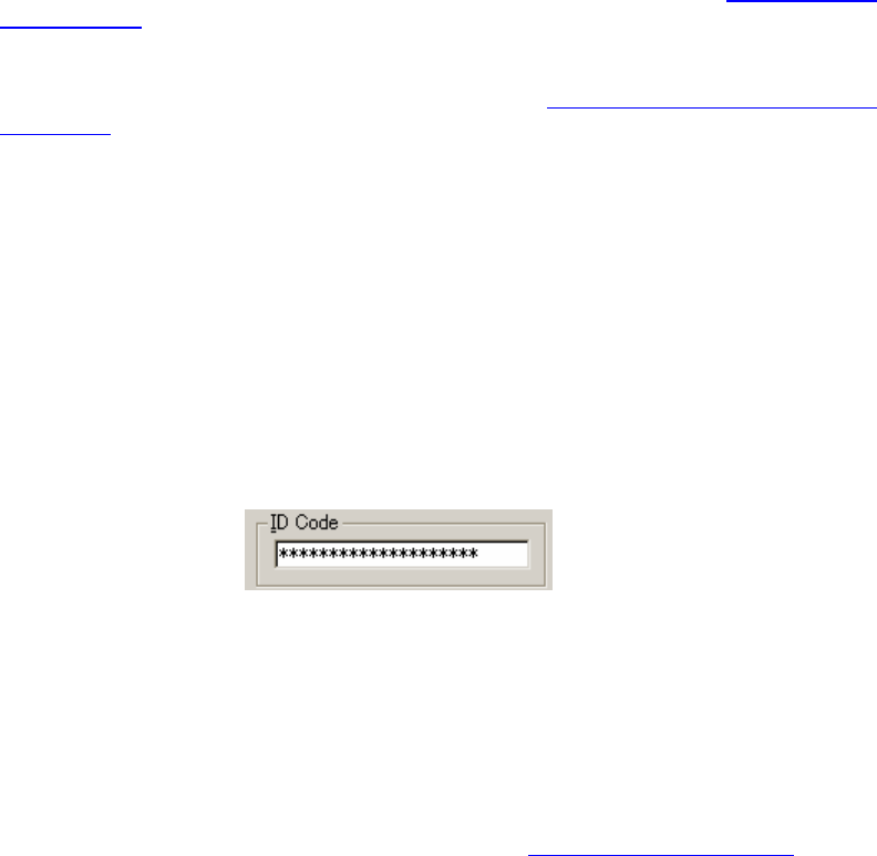
Security ID entry area at the start of debugger
Check Point 1
Enter correct security ID and click OK on the configuration window.
Check Point 2
If you forgot the security ID, you have to erase the microcontroller built-in flash
memory. Before erasing, check if you actually set the security ID with referring to
"3.4Configuration of Linker Option". Also remember the code you set for the security
ID.
After this, erase the flash memory with referring to "6.4Erase of flash memory".

- 84 -
5.2.3 "The on-chip debug function had been disabled in the device."
(F0c79)
This error occurs when the value at address C3H (On-chip debug option byte) in
microcontroller built-in flash memory is incorrect. You need to erase the flash memory.
Check Point 1
Check if you actually set the correct on-chip debug option byte with referring to
"3.4Configuration of Linker Option". If it is not correct, then set correctly.
Check Point 2
Erase the flash memory with referring to "6.4Erase of flash memory".
5.2.4 "Disabling the on-chip debug function is prohibited." (F0c33)
Basically, this error occurs when you start (download) the debugger without doing the
settings described at "3.4Configuration of Linker Option". Do the same checking processes
as"4.2.3 The on-chip debug function had been disabled in the device. (F0c79)".
- 85 -
6 Other Information
This chapter explains some useful operation techniques of development tools and
circuit diagram of the kit for developing of user programs.
7.1 Create a new workspace (project)
7.2 Register additional source file
7.3 Debugger tips
7.4 Erase microcontroller built-in flash memory
7.5 Circuit diagram
- 86 -
6.1 Create a new workspace
Now, create a new workspace and project.
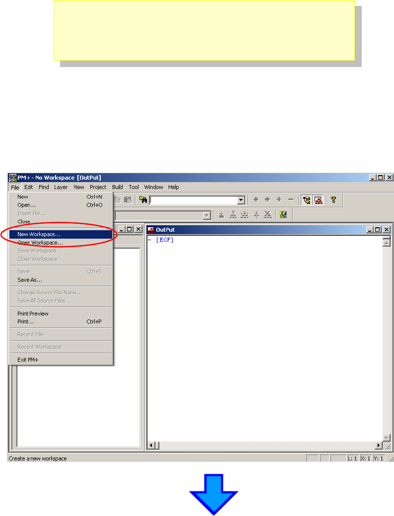
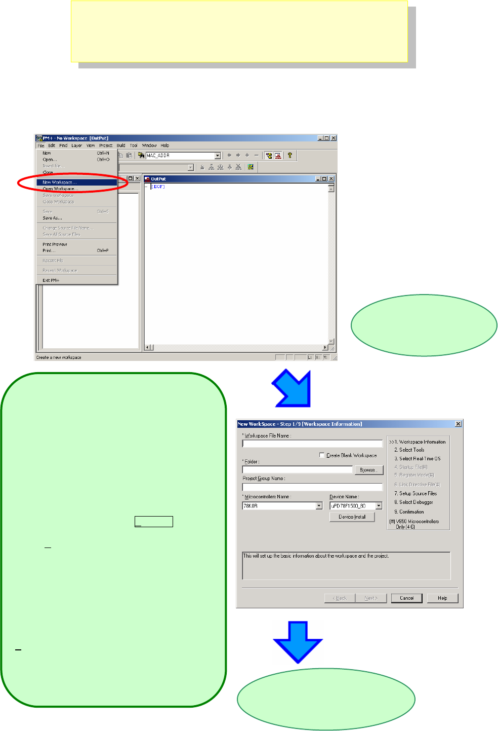
PM+ allows you to create a new workspace with following "New WorkSpace"
dialog.
Select "File" on PM+ menu bar, then "New Workspace...".
"New WorkSpace" dialog
opens
The concrete information set here is
described on the following pages
<Description of items>
Workspace File Name:
-> Specify the name of the workspace file that
manages the project files.
.prw is automatically suffixed as the file type.
A project file (.prj) of the same name is
simultaneously created.
Folder:
-> Specify the folder for saving the workspace file by
writing its absolute path.
This item can be selected from a reference
dialog box by pressing the Browse… button.
Project Group Name:
-> Specify this item if wishing to manage
multiple projects together in function units.
If nothing is specified, this item is the same as
the workspace file name.
Microcontroller Name:
-> Specify the name of the microcontroller to be
used.
Device Name:
-> Specify the name of the device to be used.
- 87 -
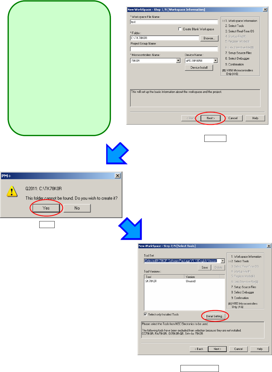
Click Next > button
Click Yes button
Click Detail Setting button
Input the workspace information setting
as follows.
Workspace file name
→ test
Folder
→ C:¥TK78K0R
Project Group Name
→ (no input)
Microcontroller Name
→ 78K0R
Device Name
→ uPD78F8058
- 88 -
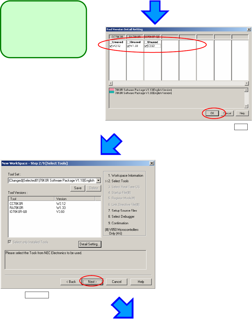
Set the version of tools as
follows.
CC78K0R:W2.12
RA78K0R:W1.33
ID78K0R-QB:V3.60
Select tools as above screenshot, then click OK .
Click Next >
- 89 -
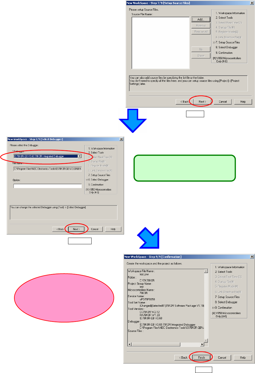
Select ID78K0R-QB V3.60
Click Next >
Click Next >
Click Finish
Check the project information
settings
- 90 -
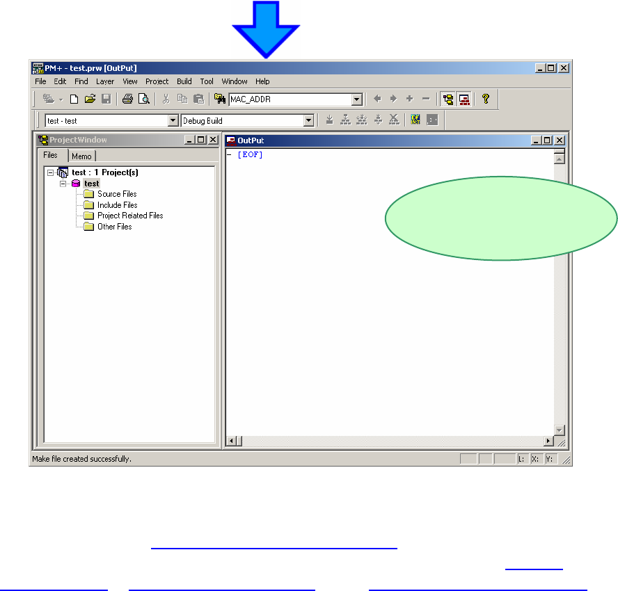
This completes workspace and project creation.
Additional source files can be registered at any time thereafter.
For details, refer to "7.2 Register additional source file".
Also, you need to do the settings for on-chip debug. Please refer to "3.4 Set
Linker Options", "3.5 Set Compiler Options", and "3.7 Check Debugger Settings".
Project “test" was registered.
- 91 -
6.2 Registration of new source files
Now, we learn how to register new source files.
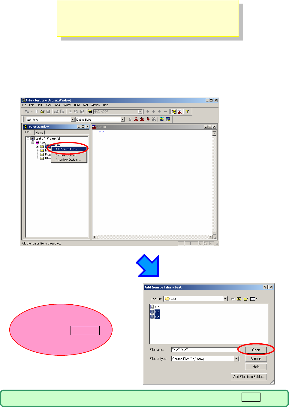
The following example shows how to register two additional source files of “b.c”
and “c.c” with source file “a.c” already registered.
Place the cursor on a source file in the Project window of PM+, and select [Add
Source Files…] displayed in the right-click menu.
Select source files "b.c" and
"c.c", then click Open
Multiple source files can be selected by clicking them while keep pressing Ctrl key.
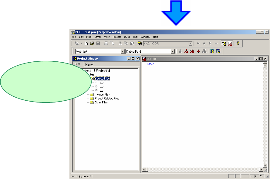
- 92 -
Source files "b.c"
and "c.c" are added
to the project.
- 93 -
6.3 Debugger tips
This section describes some useful techniques for the debugger (ID78K0R-QB).
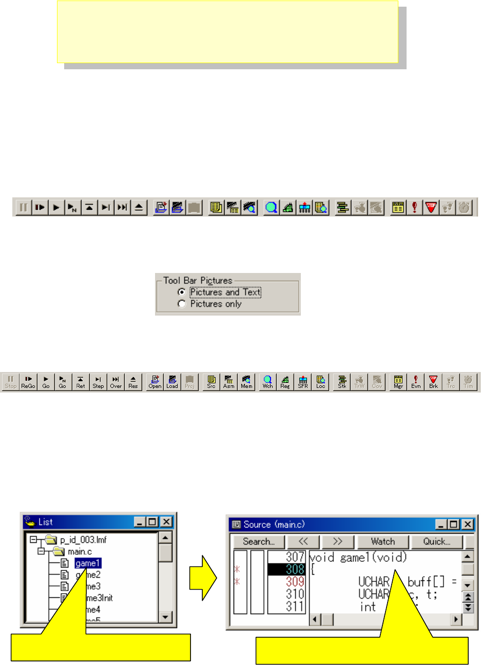
6.3.1 Change display of buttons
Execution controls (run, stop, step-in debugging, reset, etc) and opening
functional window can be made by below buttons. However, it could be difficult
to know which button does what.
In this case, select "Options" on menu bar, then "Debugger Options". Check
"Pictures and Text" on setting area.
With this setting, the buttons display the text as well, so that it is easier to know
what they are.
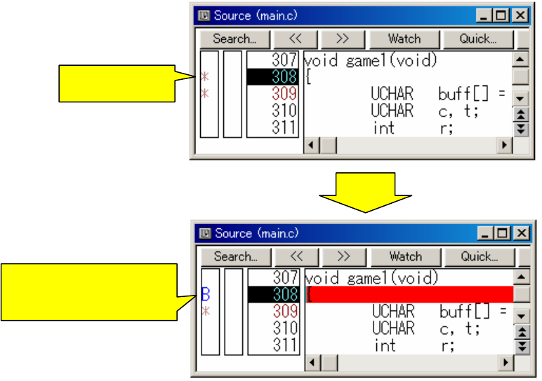
6.3.2 Display source list and function list
When you wish to see source file list or function list, select "Browse" on menu
bar, then "Other" -> "List" to open the list window. The information in the
windows is synchronized. Therefore, it is not just for referring to the list, but it is
useful when you wish to update files or functions.
When you click "game1"... Source window shows "game1"
- 94 -
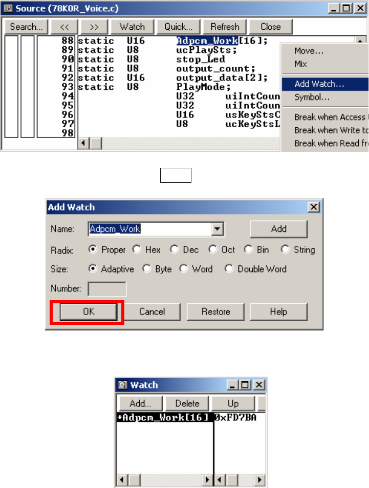
6.3.3 Set/delete breakpoints
Breakpoints are executed by clicking lines in which " * " is displayed
"B" is displayed in the line where a breakpoint is set.
Breakpoints are deleted by clicking "B".
Click
Breakpoint was set
- 95 -
6.3.4 Display global variables
With using Watch Window, you can display global variables. There are several
ways to register global variables to watch window. In this section, how to
register from source window is described.
①Right-click the variable on source window, then select "Add Watch..."
②Add Watch dialog opens. Click OK .
③Adding a variable to watch window is completed.
- 96 -
6.3.5 Display global variables while programs are running
RAM, general-purpose register, and SFR can be referred by the pseudo
real-time monitor function even when the programs are running.
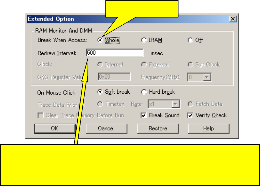
Select "Option" on menu bar, then "Extended Option...". Configure the settings
for "RAM Monitor And DMM".
This completes the settings.
Note:
・ The user program momentarily breaks upon a read.
・ Do not use the pseudo real-time monitor function while using the memory
window. It uses the system resources significantly as it monitors the
displaying memory as well.
・ It is recommended to close the memory window when you use the pseudo
real-time monitor function.
Check
Specify the sampling interval time of the pseudo real-time monitor function.
The sampling time can be specified from 0 to 65500 with unit of 100ms.
It will not monitor if it is set to "0" or blank.
- 97 -
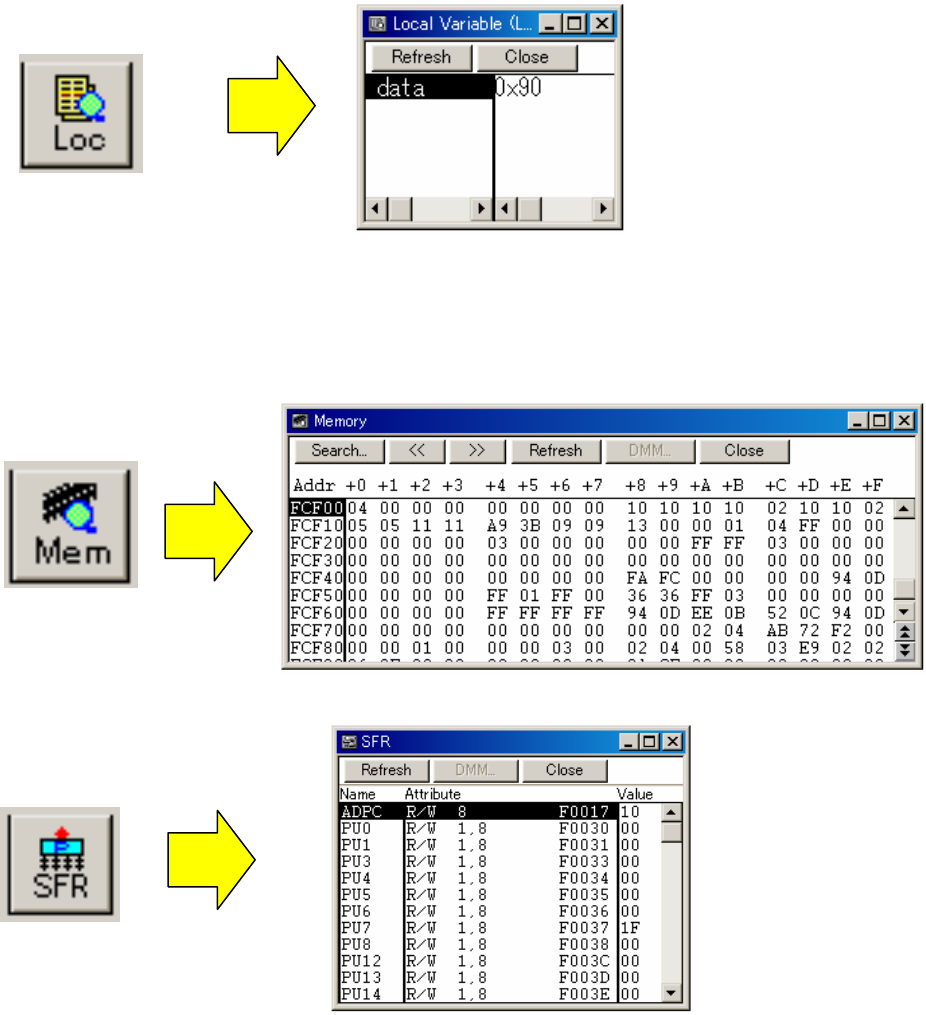
6.3.6 Display local variables
Local variable window is used to display local variables.
By clicking the button below, you can open the local variable window.
Unlike global variables, local variables cannot be displayed when programs are
running.
6.3.7 Display memory and SFR contents
By clicking the button below, you can open the memory window.
By clicking the button below, you can open the SFR window.
- 98 -
6.4 Erase of flash memory
If the On-Chip Debug Option Byte is set to "Do not erase data of flash memory in
case of failures in enabling on-chip debugging" and if you forget the security ID,
you need to erase the flash memory completely.
To erase the flash memory, please follow the steps below.
WriteEZ5 is installed at "1.2.2 Installation of Development Tools".
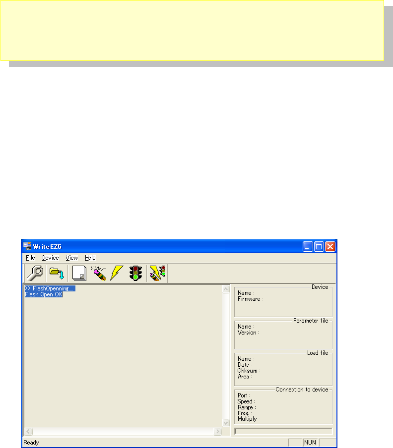
① Start WriteEZ5 by selecting "Windows Start" menu, "Programs", "NEC Electronics Tools",
"WriteEZ5", "V1.00", and "WriteEZ5".
- 99 -
② The switch of TK-RF8058+SB is set as follows.
③ Then, please connect the “USB1” connector on the TK-RF8058+SB board with the USB
connector of your PC.
SW4 setting
1 2 3 4 5 6 7 8
ON ON ON ON ON ON OFF OFF
JP5:Any
JP3:
1-2 short (USB)
SW5:3.0V
SW6:
「Debug/Writer」
JP2:
1-2 short(Regulator)
JP1:short JP4:short
- 100 -
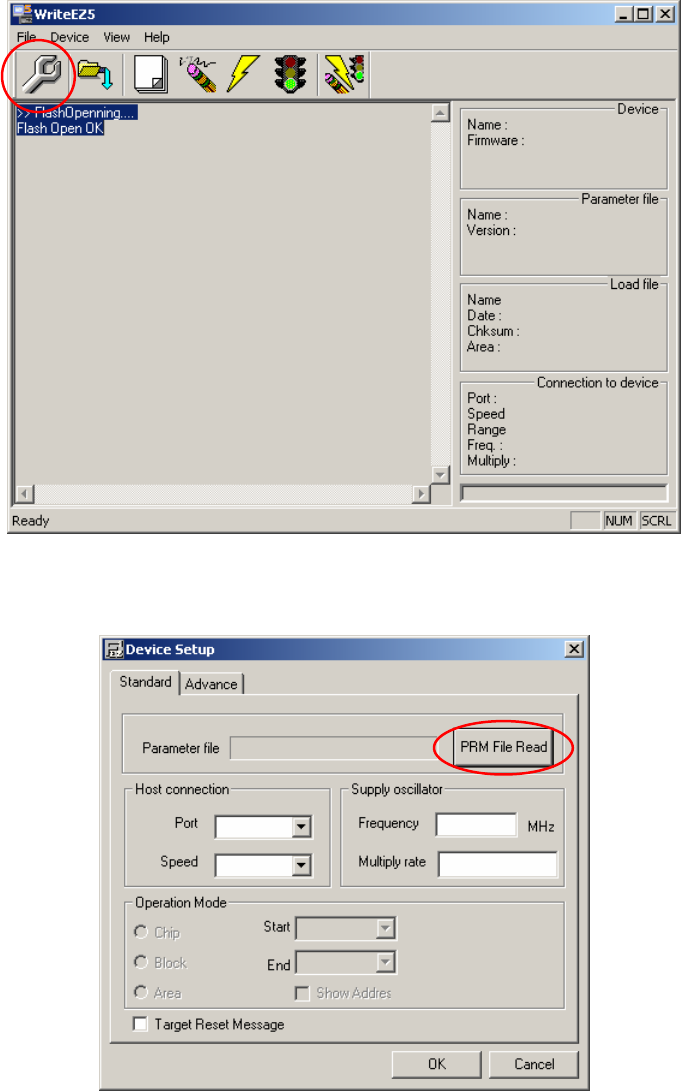
④ Push the「Setup」button.
⑤ Push the「PRM File Read」button.
- 101 -
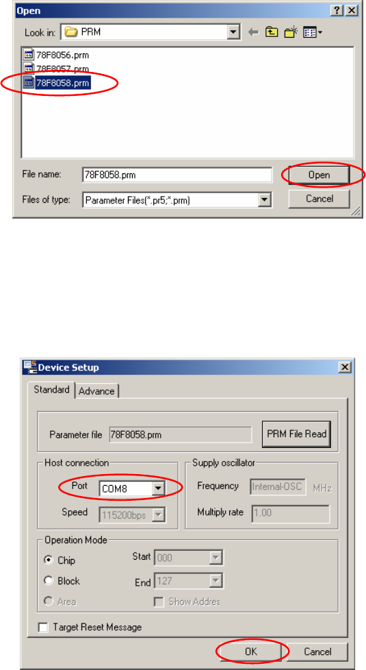
⑥ Please select “78F8058.prm” in the directory of “¥PRM” in the CD-ROM.
⑦ "Port" selects the COM port number where TK-RF8058+SB is allocated.
*Only the COM port number that the personal computer has is displayed in this pull-
down menu.
- 102 -
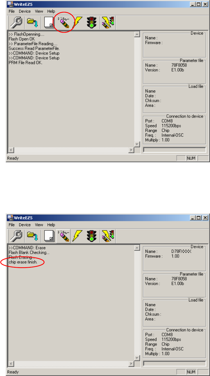
⑧ "Erase" The deletion of the flash memory begins when the button is pushed.
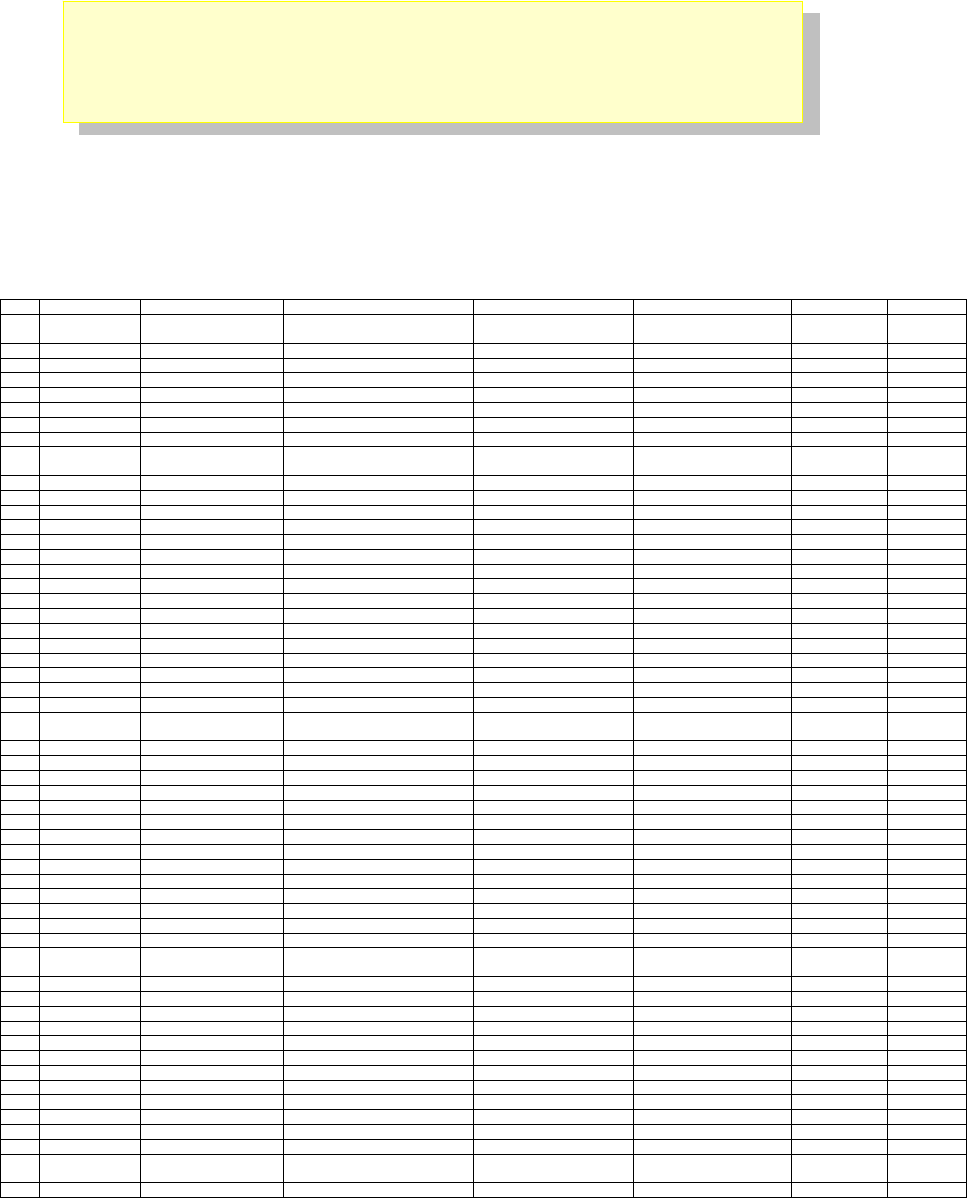
⑨ If Flash EEPROM has been erased successfully, “chip erase finish” will be displayed as
shown below.
- 103 -
※ ID Code
The ID Code is a mechanism to prevent an unwelcome third party from accessing your
source code by initiating the debugger. Therefore, it is recommended to modify the ID Code
from the default value to secure your original source code. However, once you modify it, then,
if you forget the security ID or mistakenly over-write 0x00(value) to the address of 0xC3, the
debugger ID78K0R-QB is unable to access to the CPU via OCD interface. In this case, you
have to start over from erasing all data in the Flash EEPROM. Then, you can define the new
ID Code. You may load your source code from the debugger with a load module file.
- 104 -
6.5 BOM List, Circuit diagram & Pin Connection
Here is the BOM List, circuit diagram & Pin Connection of the evaluation kit.
● SB-UD board BOM list
No. Mount Quantity Mount Parts Reference Unmount Parts Reference Type Parts No Maker Note
1 0 S_SW1,S_LED1,A/D1,S_SW2, Short Pad SS
S_LED2,A/D2,S_SW3,S_LED3
2 0 SO,SI,SCK Short Pad SO
3 2 BT1,BT2 Batt case 2460 KEYSTONE
4 0 CN1 Connecter HIF3H-50DA-2.54DSA HIROSE
5 0 CN2 Connecter HIF3H-20DA-2.54DSA HIROSE
6 1 C1 Chip ceramic cap 2.2uF
7 1 C2 Tantal cap F931A476MCC NICHICON
8 1 C3 Chip ceramic cap 10uF
9 8 C6,C7,C11,C12,C13, C4,C5 Chip ceramic cap 0.1uF
C14,C15,C16
10 2 C10,C8 Chip ceramic cap 0.47uF
11 1 C9 Aluminum Electrolytic Cap 4.7uF/25V
12 1 FP1 Connecter HIF3FC-16PA-2.54DSA HIROSE
13 2 JP1,JP4 Connecter FFC-2AMEP1 HONDA
14 3 JP2,JP3,JP5 Connecter FFC-3AMEP1 HONDA
15 1 J1 Connecter DF17(3.0)-60DS-0.5V(57) HIROSE
16 1 J2 Terminal T-16-Red SATO PARTS
17 1 J3 Terminal T-16-Black SATO PARTS
18 3 LED1,LED2,LED3 LED SML-311UTT86 STANLY
19 1 LED4 LED PG1112H ROHM
20 1 L1 inductor CDRH5D28NP-8R2NC Sumida
21 1 L2 Filter BLM41PG750S MURATA
22 1 MR1 resister module CN1E4K-105J KOA
23 0 P2,P1 Connecter XR2C-1011N OMRON for A&D
24 1 Q1 IC TPS851 TOSHIBA
25 2 R1,R44 Chip resister 120
26 8 R2,R3,R4, R24,R25,R26,R28 Chip resister 1.5K
R32,R33,R38,R42,R45
27 1 R5 Chip resister 7.5K
28 2 R7,R8 Chip resister 390K
29 1 R16 Chip resister 487K
30 1 R17 Chip resister 562K
31 1 R18 Chip resister 909K
32 2 R20,R21 Chip resister 187K
33 1 R22 Chip resister 182K
34 4 R27,R34,R37,R43 R29,R31 Chip resister 100K
35 2 R39,R40 R30 Chip resister 27
36 4 R6,R35,R36,R41 Chip resister 10K
37 0 Chip resister 100
38 4 SW1,SW2,SW3,SW7 Switch SKQMBB ALPS
39 1 SW4 Switch CHS-08B COPAL
40 2 SW6,SW5 Switch SSSS223600 ALPS
41 0 TPU1,TPU2,TPU3,TPU4,TPU5, Trough hole TPU
TPU6,TPU7,TPU8,TPU9
42 0 TP1,TP2,TP3,TP4,TP5 Terminal LC-2 MAC8
43 1 USB1 Connecter UX60A-MB-5ST HIROSE
44 1 U1 IC S-8120CNB SII
45 1 U2 IC TPS61020DRC TI
46 0 U3 IC SN74LVC3G07DCT TI For SIO I/F
47 1 U5 U4 IC SN74LVC2G125DCU TI
48 1 U6 IC SN74LVC2G07DCK TI
49 1 U7 IC UPD78F0730MC NECEL
50 1 U8 IC SN74LVC1G125DCK TI
51 1 U9 IC SN74LVC2T45DCU TI
52 1 Y1 IC CSTCE16M0V53-R0 MURATA
53 5 JP1,JP2,JP3,JP4,JP5 Jumper HIF3GA-2.54SP HIROSE
54 0 R9,R10,R12,R13,R14, Chip resister For K0R
R15,R19
55 3 R11,R23,R46 Chip resister 0 For K0R

- 105 -
● MB-RF8058 board BOM list
No. Mount Quantity Mount Parts Reference Unmount Parts Reference Type Parts No Manufacturer
1 1 CN1 Connecter 901-144-8RFX AMPHENOL
2 5 C2,C5,C6,C11,C15 Chip ceramic cap 47pF
3 4 C4,C7,C10,C16 Chip ceramic cap 0.01uF
4 2 C8,C18 Chip ceramic cap 1uF
5 1 C9 Chip ceramic cap 39pF
6 1 C12 Chip resister 0
7 2 C24,C13 Chip ceramic cap 0.1uF
8 3 C14,C1,C3 Chip ceramic cap 10pF
9 1 C17 Chip ceramic cap 0.47uF
10 1 C19 Chip ceramic cap 4.7uF/10V
11 2 C23,C20 Chip ceramic cap 10uF/10V
12 1 C21 Chip ceramic cap 3pF
13 1 C22 Chip ceramic cap 4pF
14 1 F1 Filter LDB212G4020C-001 MURATA
15 1 J1 Connecter DF17(2.0)-060DP-0.5V(57) HIROSE
16 1 L1 inductor LQG15HN3N9S02 Murata
17 1 L2 inductor LQH2MCN8R2M02 MURATA
18 0 L3,L4 inductor
19 1 R1 Chip resister 1M
20 7 R2,R4,R5,R7,R8,R9,R10 Chip resister 10K
21 1 R3 Chip resister 0
22 0 R6 Chip resister
23 0 TP1,TP2,TP3,TP4 Check Pin LC-33
24 1 U1 IC uPD78F8058 NECEL
25 0 VDD_R,VDD Short pad SS
26 1 Y1 Resonator NX3225SA-32.000M-STD-CSR-3 NDK
27 1 Y2 Resonator SSP-T7-FL 3.7pF SII
- 106 -
I/O_40
IOVDD
IOVDD
IOVDD
IOVDD IOVDD IOVDD
IOVDD
JP1
FFC-2AMEP1
1 2
IOVDD
R23xxx
I/O_40
T_RESET
TOOL0 TOOL1
I/O_34
I/O_39
I/O_38I/O_37
I/O_36I/O_35
SW4-6
CHS-08B
611
TP1
LC-2
IOVDD
R6
1.5K
No Mount
RESET2
FLMD02
RxD_MCU2
TOO L02
TxD_MCU 2
TOOL1 2
1pin : 3.0V
Center : 2.0V
4pin : 1.8V
A/D 2
1-2 : 1Cell
2-3 : 2Cell
Regulator Input
1-2 : USB
2-3 : Battery
VDD
1-2 : Regulator
2-3 : Battery or External
Current Measure
126 Parts, 33 Library Parts, 136 Nets, 490 Pins
1.VDD
2.FLMD0
3.RESET
4.P41/TOOL1
5.P40/TOOL0
6.GND
7.P30/INT3
8.P74/KR4/INTP8
9.P14/RxD3
10.GND
11.VDD
12.SCK10
13.SI10(/RxD1)
14.SO10(/TxD1)
15.P13/TxD3
16.GND
17.P75/KR5/INTP10
18.P76/KR6/INTP11
19.P77/KR7/INTP12
20.GND
1V
No Mount
T_R ES ET2
SW4-7
CH S-08B
710
SW4-8
CH S-08B
89
I/O_02
I/O_01
I/O_03
TxD_MCU
TOOL1
TP2
LC-2
TP3
LC-2
MINICUBE2 I/F
Illuminance Sensor
Temp. Sensor
MINICUBE2 I/F
Tit l e
Size Document N umber Rev
Dat e: Sheet of
TS-TCS00327 1. 0
SB-UD
A3
12Monday , Sept ember 14, 2009
P_SW1
P_SW2
P_SW3
T_R ESET
FLMD0
RESET
TxD_MCU
RxD_MCU
RESET
FLMD0
RxD_MCU
TOOL1
TOOL0
I/O_14
I/O_23
I/O_07
I/O_09
I/O_21
I/O_31
TOOL0
RESET
TOO L0
I/O_01
I/O_06
I/O_24
I/O_33
Tx D _MC U
I/O_26
LED2
I/O_05
I/O_08
LED3P_SW3
I/O_12
TOOL1
I/O_29
I/O_11
I/O_30
P_SW2
I/O_13
I/O_18
FLMD1
A/D3
LED3P_SW3
A/D2LED2
P_SW2A/D1
LED1P_SW1
I/O_03I/O_02
I/O_01RxD_MCU
TxD_MCUFLMD1
I/O_19
I/O_18I/O_17
I/O_16I/O_15
I/O_14I/O_13
I/O_12I/O_11
I/O_10I/O_09
I/O_08I/O_07
I/O_06I/O_05
I/O_04
I/O_33
I/O_32I/O_31
I/O_30I/O_29
I/O_28I/O_27
I/O_26I/O_25
I/O_24I/O_23
I/O_22I/O_21
I/O_20
LED1LED1
P_SW2
P_SW1
P_SW1
I/O_01
I/O_03
I/O_02
P_SW3
A/D1
R2
1.5K
J3A
T-16-Bl a c k
1
FP1
HI F3FC-16PA-2.54DSA
GND
1
SI
3
SO
5
7
7
9
9
11
11
13
13
RESET_IN
15
RES 2
VDD 4
66
88
10 10
12 12
FL0 14
CLK_IN 16
LED3
SML-311UTT86
S_LED2
SW5
SSSS223600
124568
37
R17
562K
SW3
SKQMBB
12
R9xxx
LED4
PG1112H
SW1
SKQMBB
12
SCK
U2
TPS61020DRC
SW
9
VBAT
6
EN
1
LBI
7
PS
8
GND
5
VOUT 2
FB 3
LBO 4
PGND 10
G_PAD 11
JP2
FFC-3AMEP1
2
1
3
LED1
SML-311UTT86
R7
390K
U1
S-8120CNB
VDD 1
VOUT
4
VSS 2
NC
3
L1
8.2uH
JP4
FFC-2AMEP1
1 2
Q1
TPS851
2
15
34
JP5
FFC-3AMEP1
2
1
3
1.5V
R16
487K
S_LED1
3V
P2
XR2C-1011N
1
2
3
4
5
6
7
8
9
10
S_LED3
R22
182K
S_SW3
R15xxx
C2
47uF
A/D2
A/D1
R21
187K
BT1
2460
JP3
FFC-3AMEP1
2
1
3
SW2
SKQMBB
12
R13xxx
LED2
R11xxx
R19xxx
SI
R5
7.5K
R3
1.5K
CN1
HIF3H-50DA-2.54DSA
1
3
5
7
9
11
13
15
17
19
21
23
25
27
29
31
33
35
37
39
41
43
45
47
49
2
4
6
8
10
12
14
16
18
20
22
24
26
28
30
32
34
36
38
40
42
44
46
48
50
R14xxx
R20
187K
BT2
2460
C1
2.2uF
S_SW2
J2A
T-16-R ed
1
P1
XR2C-1011N
1
2
3
4
5
6
7
8
9
10
C3
10uF
R8
390K
LED2
SML-311UTT86
S_SW1
SO
R1
120
R12xxx
R4
1.5K
LED1
R10xxx
J1
DF17(3.0)-60DS-0.5V(57)
2
4
6
8
10
12
14
16
18
20
22
24
26
28
30
32
34
36
38
40
42
44
46
48
50
52
54
56
58
60
1
3
5
7
9
11
13
15
17
19
21
23
25
27
29
31
33
35
37
39
41
43
45
47
49
51
53
55
57
59
LED2
R18
909K
USBVDD
VDD
VDD
VDD
VDD VDD
USBVDDUSBVDD
EXTVDDEXTVDD
EXTVDD
LED3
SO_MCU 2
SCK_MCU 2
SI_MCU 2
RxD_MCU
I/O_02 I/O_03
A/D 1
A/D 2
A/D 3 I/O_04
TP4
LC-2
TP5
LC-2 VDD
GND VDD
POWER
I/O_10
I/O_15 I/O_16
I/O_17
I/O_19 I/O_20
I/O_22
I/O_25
I/O_27
GND
VDD
I/O_28
I/O_32
I/O_34
I/O_35 I/O_36
CN2
HIF3H-20DA-2.54DSA
1
3
5
7
9
11
13
15
17
19
2
4
6
8
10
12
14
16
18
20
I/O_37 I/O_38
I/O_39
● SB-UD board schematic
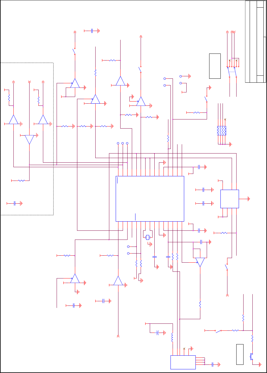
- 107 -
IOVDD
IOVDD
IOVDD
IOVDD
Tx D 6U S B
RxD6USB
↑K0R<-->K0USB
↓Debug/Writer
IOVDD
IOVDD
IOVDD
IOVDD
RxD6USB
FLMD0U
TxD6USB
TOO L1_S W
PD6
PD1
PD5
RxD6USB
PD1
Mounted only 78K0.
PD5
PD6
FLMD0U
IOVDD
IOVDD
IOVDD
TOOL1_SW
Mounted only SIO.
Mounted only 78K0.
Mounted only 78K0.
Mounted only 78K0.
Mounted only 78K0.
Mounted only 78K0.
Mounted only 78K0.
Mounted only 78K0.
Mounted expect 78K0.
Tit le
Size Document Number Rev
Dat e: Sheet of
TS-TCS00327 1.0
SB-UD
A3
22Monday , Sept ember 14, 2009
(Shield)
R42 1.5K
12
R37
100K
R29
100K
U8
SN74LVC1G125DC K
24
5
1
3
U3B
SN74LVC3G07DC T
35
84
U6A
SN74LVC2G07DCK
1 6
5
2
U7
UPD 78F0730MC
P30/INTP1
1
P01/TI010/TO00
2
P00/TI000
3
P120/IN TP0/EXLVI
4
RESET
5
FLMD0
6
P122/X2/EXCLK/OCD 0B
7
P121/X1/OC D0A
8
REGC
9
Vss
10
Vdd
11
USBREGC
12
USBP
13
USBM
14
USBPU C
15
P10/SCK10 30
P11/SI10 29
P12/SO10 28
P13/TxD6 27
P14/RxD6 26
P15 25
P16/TOH1 24
P17/TI50/TO50 23
P33/TI51/TO51 22
EVss 21
EVdd 20
P31/INTP2/OCD1A 19
P32/INTP3/OCD1B 18
P60 17
P61 16
R41
10K
1 2
R36 10K
12
C13
0.1uF
R28
1.5K
TPU 8
1
SW4-1
CHS-08B
116
SW4-3
CHS-08B
314
U3A
SN74LVC3G07DC T
1 7
8
4
TPU 11
C12
0.1uF
TPU 6
1
TPU 9
1
R43
100K
TPU 5
1
SW6
SSSS223600
1
2
4
5
6
8
3
7
SW4-2
CHS-08B
215
R25
1.5K
U6B
SN74LVC2G07DC K
3 4
5
2
C11
0.1uF
C8
0.47uF
+
C9
4.7uF/ 25V
R31
100K
U9
SN74LVC2T45DCU
VCCA
1
GND
4
A1
2B1 7
VCC B 8
DIR
5
A2
3B2 6
SW4-4
CHS-08B
413
R35 10K
12
R40 27
1 2
R39 27
1 2
U5B
SN74LVC2G125DCU
5 3
8
7
4
U4A
SN74LVC2G125DCU
2 6
8
1
4
C6
0.1uF
R27
100K
R33
1.5K
TPU 21
C10 0. 47uF
TPU 7
1
R44
120
12
C16
0.1uF
C15
0.1uF
12
MR1
CN1E4K-105J
18
27
36
45
USB1
UX60A-MB-5ST
VBUS 1
D- 2
D+ 3
ID_NC 4
GND 5
FG1
FG1 FG2
FG2 FG3
FG3 FG4
FG4
TPU 4
1
C14
0.1uF
12
R34
100K
R26
1.5K
C5
0.1uF
TPU 31
C7
0.1uF
R46
0
1 2
U5A
SN74LVC2G125DCU
2 6
8
1
4
R32
1.5K
R45
1.5K
1 2
U4B
SN74LVC2G125DCU
5 3
8
7
4
R38 1.5K
1 2
R24
1.5K
U3C
SN74LVC3G07DC T
6 2
8
4
L2
BLM41PG750S
Y1
CSTCE16M0V53-R0
13
2
SW7
SKQMBB
1 2
R30
27
USBVDD
USBVDD
USBVD DUSBVD D
USBVDD
USBVDD
USBVDD
IOVDD
USBVDD
USBVDD
USBVDD
USBVDD
RESET 1
TOO L0 1
TOO L11
FLMD0 1
T_R ES ET1
SO_MCU 1
Tx D _MC U 1
RxD_MCU 1
SI_MCU 1
SCK_MCU 1
RESET SW
T_R ES ET
RESET
C4
0.1uF
SW4-5
CHS-08B
512
IOVDD
IOVDD
IOVDD
IOVDD
IOVDD
IOVDD
IOVDD
IOVDD
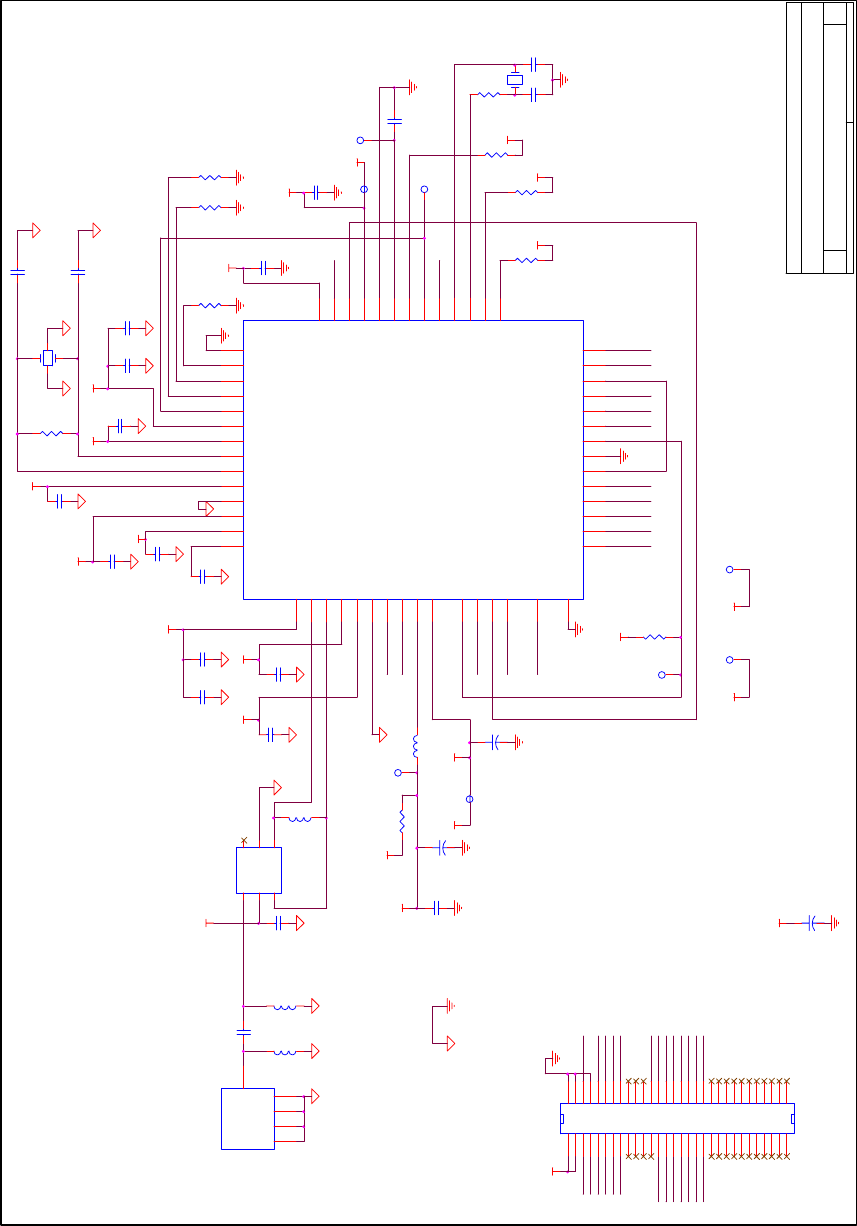
- 108 -
LED1
SCAN_MODE
SCAN_EN
SCK
SO/TxD
SI/RxD
SW3
SW2
LED3
LED2
R2
10K
I2CSEL
C5
47pF
Y2
SSP-T7-FL 3.7pF
C22
4pF
R3
0
C21
3pF
A/D1(Temp) A/D2(Illum i)
VDD
GPIO0
P14
C8
1uF
P13
U1
uPD78F8058
GND_D 28
GND_GR
47
GND_PLL 38
VDD_A 34
VDD_BG 33
VDD_CP 39
VDD_D 27
VDD_GR
46
VDD_PLL 37
VDD_RF1
42
VDD_RF2
45
VDD_VCO 40
CLK_OUT 32
GPIO0
48
GPIO1
49
P15(/GPI O2)
55
P16(/GPI O3)
53
VDD_3V(/AVDD)
51
VDD_2V2
50
I2CSEL 29
LOOP_C 41
RF_N
44
RF_P
43
SCAN_EN 30
SCAN_MODE 31
XTAL_N 35
XTAL_P 36
RESETn
52
GND_pad
57
INT
54
P13/TxD3
1
(SI/P12/SC00)
2
(SO/P11/SI00)
3
(SCLK/P10/SCK00)
4
(SEN/P17)
5
WAKE
6
AVSS
7
P41/TOOL1
14
P144
12
P120
13
P02/SO10/TxD1
11
P03/SI10/ RxD1
10
P130
8
P04/SCK1
9
P124/XT2 17
FLMD0 19
REGC 22
P122/X2/EXCLK 20
RESET 16
P121/X1 21
P40/TOOL0 15
P123/XT1 18
VSS 23
P31/TI03/TO03/INTP4 25
VDD 24
P76/INTP10 26
P14/RxD3
56
P04P03
P02
C11
47pF
C10
0.01uF
VDD
TOOL1
VDD_R
45 Parts, 12 Library Parts, 44 Nets, 177 Pins
TOOL0
RESET
C13
0.1uF
FLMD0
L3
xxx
TP3
LC-33
L4
xxx
P121
C15
47pF
C17 0.47uF
VDD
VDD_RF
+
C20
10uF/10V
C16
0.01uF
F1 LDB212G4020C-001
UNB
1
GND
2
BAL 4
GND 5
NC 6
BAL
3
P76
VDD_RF
FLMD0
C14
10pF
RESET
TOOL0
TOOL1
P120
L2
8.2uH
TP1
LC-33
P144-
P10-
VDD_R
P11-
TP5
LC-33
VDD_M
P12-
TP6
LC-33
P17-
P144-
P02
+
C23
10uF/10V
VDD
Tit l e
Size Document Number Rev
Date: Sheet of
TS-TCS00326 1. 0
MB-R F 8058
A3
11Friday , September 11, 2009
P03
P04
C6
47pF
C7
0.01uF
C9
39pF
C3 10pF
R8
10K
C1 10pF
C12
0
C2
47pF
R1
1M
R9
10K
L1
3.9nH
P16
Y1
NX3225SA-32.000M-STD-CSR-3
1 3
4 2
A/D3
C4
0.01uF
VDD_RF
VDD_RF
VDD_RF
GPIO1
P120
P12-
P10-
VDD_RF
SCAN_EN
P31-
P121
C24
0.1uF
P130-
GPIO0
P11-
P17-
I2CSEL
SCAN_MODE
P76
R4
10K VDD_M
R10
10K VDD_M
VDD_RF
J1
DF17(2.0)-060DP-0.5V(57)
2
4
6
8
10
12
14
16
18
20
22
24
26
28
30
32
34
36
38
40
42
44
46
48
50
52
54
56
58
60
1
3
5
7
9
11
13
15
17
19
21
23
25
27
29
31
33
35
37
39
41
43
45
47
49
51
53
55
57
59
VDD_RFVDD_R
GPIO1
+
C19
4.7uF/10V
C18
1uF
TP2
LC-33
VDD_RF
VDD
VDD_M
R5
10K VDD_M
R6
xxx
VDD_R
VDD_R
TP4
LC-33 R7
10K
VDD_R
CN1 SMA
C
3
C
2
C
4
C
5
H1
P16
P31-
P15
P14
P13
P130-
VDD_R
TxD
RxD
P15
SW1
● MB-RF8058 board schematic

- 109 -
● SB-UD board CN1 Pin connecting list
Pin number Net name uPD78F8058 Signal Port Connection Requirement for using the signal
1 VDD -
2 GND -
3 VDD -
4 GND -
5 TOOL0 -
6 TOOL1 -
7 T_RESET -
8 GND -
9 FLMD1 -
10 TxD_MCU P13/TxD3
11 RxD_MCU P14/RxD3
Don't use the USB connection as debugging or
serial communication when you use this signal.
12 I/O_01 P02/SO10/TxD1 -
13 I/O_02 P03/SI10/RxD1/SDA10 -
14 I/O_03 P04/SCK10/SCL10 -
15 P_SW1 P15/RTCDIV/RTCCL/GPIO2 Separate a switch with cutting the solder short pad
for use as general-purpose port.
16 LED1 P16/TI01/TO01/INTP5/GPIO3 Separate a LED with cutting the solder short pad
for use as general-purpose port.
17 A/D1 -
18 P_SW2 -
19 LED2 -
20 A/D2 -
21 P_SW3 -
22 LED3 -
23 A/D3 -
24 I/O_04 P120/INTP0/EXLVI -
25 I/O_05 -
26 I/O_06 -
27 I/O_07 -
28 I/O_08 -
29 I/O_09 -
30 I/O_10 -
31 I/O_11 P76/INTP10 -
32 I/O_12 P121/X1 This port has a pull-up resister.
33 I/O_13 GPIO0 RF transceiver port
34 I/O_14 GPIO1 RF transceiver port
35 I/O_15 -
36 I/O_16 -
37 I/O_17 -
38 I/O_18 -
39 I/O_19 -
40 I/O_20 -
41 I/O_21 -
42 I/O_22 -
43 I/O_23 -
44 I/O_24 -
45 I/O_25 -
46 I/O_26 -
47 I/O_27 -
48 I/O_28 -
49 I/O_29 -
50 I/O_30 -
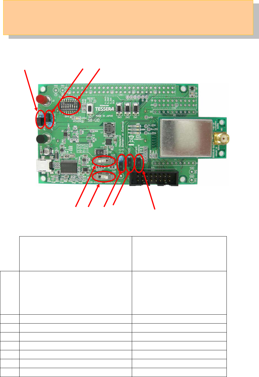
- 110 -
SW4
JP5
JP4
JP1
JP2
SW6 SW5
JP3
JP4JP2
7 Mode setting of the board
The combination table of the switch of this board is shown.
Mode Setting Table
User mode on USB power with
Debugging and Flash programming
with MINICUBE2, and UART-USB
conversion to a HyperTerminal. (NOTE)
Debug/Flash programming mode
via USB without MINICUBE2
using ID78K0R-QB/WriteEZ5
SW4
(Dip switch)
1-4 → ALL OFF
5 → ON (Pull-up the RESET pin)
6 → ON (Power LED on)
7,8 → Any
(Dip switch)
1-6 → ALL ON
7,8 → Any
SW6 「K0R-K0USB」 「Debug/Writer」
SW5 1.8V, 2.0V or 3.0V 1.8V, 2.0V or 3.0V
JP3 1-2 (USB) short 1-2 (USB) short
JP5 Any Any
JP2 1-2 short 1-2 short
JP1 short short
JP4 short short
(NOTE): The side switches of MINICUBE2 have to be set to “M1” and “T”.