THALES DIS AlS Deutschland ELS31-US LTE Module User Manual hid elsx1 us
Gemalto M2M GmbH LTE Module hid elsx1 us
User Manual
M2M.GEMALTO.COM
Cinterion® ELS31-US/ELS51-US
Hardware Interface Overview
Version: 01.000a
DocId: ELS31-US_ELS51-US_HIO_v01.000a

GENERAL NOTE
THE USE OF THE PRODUCT INCLUDING THE SOFTWARE AND DOCUMENTATION (THE "PROD-
UCT") IS SUBJECT TO THE RELEASE NOTE PROVIDED TOGETHER WITH PRODUCT. IN ANY
EVENT THE PROVISIONS OF THE RELEASE NOTE SHALL PREVAIL. THIS DOCUMENT CONTAINS
INFORMATION ON GEMALTO M2M PRODUCTS. THE SPECIFICATIONS IN THIS DOCUMENT ARE
SUBJECT TO CHANGE AT GEMALTO M2M'S DISCRETION. GEMALTO M2M GMBH GRANTS A NON-
EXCLUSIVE RIGHT TO USE THE PRODUCT. THE RECIPIENT SHALL NOT TRANSFER, COPY,
MODIFY, TRANSLATE, REVERSE ENGINEER, CREATE DERIVATIVE WORKS; DISASSEMBLE OR
DECOMPILE THE PRODUCT OR OTHERWISE USE THE PRODUCT EXCEPT AS SPECIFICALLY
AUTHORIZED. THE PRODUCT AND THIS DOCUMENT ARE PROVIDED ON AN "AS IS" BASIS ONLY
AND MAY CONTAIN DEFICIENCIES OR INADEQUACIES. TO THE MAXIMUM EXTENT PERMITTED
BY APPLICABLE LAW, GEMALTO M2M GMBH DISCLAIMS ALL WARRANTIES AND LIABILITIES.
THE RECIPIENT UNDERTAKES FOR AN UNLIMITED PERIOD OF TIME TO OBSERVE SECRECY
REGARDING ANY INFORMATION AND DATA PROVIDED TO HIM IN THE CONTEXT OF THE DELIV-
ERY OF THE PRODUCT. THIS GENERAL NOTE SHALL BE GOVERNED AND CONSTRUED
ACCORDING TO GERMAN LAW.
Copyright
Transmittal, reproduction, dissemination and/or editing of this document as well as utilization of its con-
tents and communication thereof to others without express authorization are prohibited. Offenders will be
held liable for payment of damages. All rights created by patent grant or registration of a utility model or
design patent are reserved.
Copyright © 2016, Gemalto M2M GmbH, a Gemalto Company
Trademark Notice
Gemalto, the Gemalto logo, are trademarks and service marks of Gemalto and are registered in certain
countries. Microsoft and Windows are either registered trademarks or trademarks of Microsoft Corpora-
tion in the United States and/or other countries. All other registered trademarks or trademarks mentioned
in this document are property of their respective owners.
ELS31-US_ELS51-US_HIO_v01.000a 2016-12-28
Confidential / Preliminary
Cinterion® ELS31-/ELS51-US Hardware Interface Overview
2
Page 2 of 46
Document Name: Cinterion® ELS31-/ELS51-US Hardware Interface Overview
Version: 01.000a
Date: 2016-12-28
DocId: ELS31-US_ELS51-US_HIO_v01.000a
Status: Confidential / Preliminary

Cinterion® ELS31-/ELS51-US Hardware Interface Overview
Contents
46
ELS31-US_ELS51-US_HIO_v01.000a 2016-12-28
Confidential / Preliminary
Page 3 of 46
Contents
1 Introduction ................................................................................................................. 7
1.1 Key Features at a Glance .................................................................................. 7
1.2 ELS31-US/ELS51-US System Overview ......................................................... 10
2 Interface Characteristics .......................................................................................... 11
2.1 Application Interface ........................................................................................ 11
2.1.1 USB Interface...................................................................................... 11
2.1.2 Serial Interface ASC0 ......................................................................... 12
2.1.3 Serial Interface ASC1 ......................................................................... 13
2.1.4 UICC/SIM/USIM Interface................................................................... 14
2.1.5 GPIO Interface .................................................................................... 16
2.1.6 I2C Interface ........................................................................................ 17
2.1.7 SPI Interface ....................................................................................... 17
2.1.8 Pulse Counter ..................................................................................... 17
2.1.9 HSIC Interface (ELS51-US Only)........................................................ 17
2.1.10 SDIO Interface (ELS51-US Only) ....................................................... 18
2.1.11 Control Signals.................................................................................... 19
2.1.11.1 Status LED .......................................................................... 19
2.1.11.2 Fast Shutdown .................................................................... 19
2.2 RF Antenna Interface....................................................................................... 20
2.2.1 Antenna Installation ............................................................................ 21
2.2.2 RF Line Routing Design...................................................................... 22
2.2.2.1 RF Interface Signals Circuit Diagram Example................... 22
2.2.2.2 Line Arrangement Examples ............................................... 23
2.3 Sample Application .......................................................................................... 28
3 Operating Characteristics ........................................................................................ 30
3.1 Operating Modes ............................................................................................. 30
3.2 Power Supply................................................................................................... 30
4 Mechanical Dimensions, Mounting and Packaging............................................... 31
4.1 Mechanical Dimensions of ELS31-US/ELS51-US ........................................... 31
5 Regulatory and Type Approval Information ........................................................... 33
5.1 Directives and Standards................................................................................. 33
5.2 SAR requirements specific to portable mobiles ............................................... 35
5.3 Reference Equipment for Type Approval......................................................... 36
5.4 Compliance with FCC and IC Rules and Regulations ..................................... 37

Cinterion® ELS31-/ELS51-US Hardware Interface Overview
Contents
46
ELS31-US_ELS51-US_HIO_v01.000a 2016-12-28
Confidential / Preliminary
Page 4 of 46
6 Document Information.............................................................................................. 39
6.1 Revision History ............................................................................................... 39
6.2 Related Documents ......................................................................................... 39
6.3 Terms and Abbreviations ................................................................................. 39
6.4 Safety Precaution Notes .................................................................................. 43
7 Appendix.................................................................................................................... 44
7.1 List of Parts and Accessories........................................................................... 44

Cinterion® ELS31-/ELS51-US Hardware Interface Overview
Tab les
46
ELS31-US_ELS51-US_HIO_v01.000a 2016-12-28
Confidential / Preliminary
Page 5 of 46
Tables
Table 1: Signals of the SIM interface (SMT application interface) ............................... 14
Table 2: GPIO lines and possible alternative assignment............................................ 16
Table 3: SDIO interface features.................................................................................. 18
Table 4: SDIO interface lines ....................................................................................... 18
Table 5: Return loss in the active band........................................................................ 20
Table 6: Overview of operating modes ........................................................................ 30
Table 7: Directives ....................................................................................................... 33
Table 8: Standards of North American type approval .................................................. 33
Table 9: Standards of GCF type approval.................................................................... 33
Table 10: Requirements of quality ................................................................................. 33
Table 11: Standards of the Ministry of Information Industry of the
People’s Republic of China............................................................................ 34
Table 12: Toxic or hazardous substances or elements with defined concentration
limits............................................................................................................... 34
Table 13: Antenna gain limits for FCC and IC (TBD)..................................................... 37
Table 14: List of parts and accessories.......................................................................... 44
Table 15: Molex sales contacts (subject to change) ...................................................... 45

Cinterion® ELS31-/ELS51-US Hardware Interface Overview
Figures
46
ELS31-US_ELS51-US_HIO_v01.000a 2016-12-28
Confidential / Preliminary
Page 6 of 46
Figures
Figure 1: ELS31-US/ELS51-US system overview......................................................... 10
Figure 2: USB circuit ..................................................................................................... 11
Figure 3: Serial interface ASC0..................................................................................... 12
Figure 4: Serial interface ASC1..................................................................................... 13
Figure 5: External UICC/SIM/USIM card holder circuit ................................................. 15
Figure 6: RF interface signals example......................................................................... 22
Figure 7: Embedded Stripline with 65µm prepreg (1080) and 710µm core .................. 23
Figure 8: Micro-Stripline on 1.0mm standard FR4 2-layer PCB - example 1 ................ 24
Figure 9: Micro-Stripline on 1.0mm Standard FR4 PCB - example 2............................ 25
Figure 10: Micro-Stripline on 1.5mm Standard FR4 PCB - example 1............................ 26
Figure 11: Micro-Stripline on 1.5mm Standard FR4 PCB - example 2............................ 27
Figure 12: Schematic diagram of ELS31-US/ELS51-US sample application.................. 29
Figure 13: ELS31-US/ELS51-US– top and bottom view................................................. 31
Figure 14: Dimensions of ELS31-US/ELS51-US (all dimensions in mm) ....................... 32
Figure 15: Dimensions of ELS31-US/ELS51-US (all dimensions in mm) - bottom view. 32
Figure 16: Reference equipment for Type Approval ....................................................... 36
Cinterion® ELS31-/ELS51-US Hardware Interface Overview
1 Introduction
10
ELS31-US_ELS51-US_HIO_v01.000a 2016-12-28
Confidential / Preliminary
Page 7 of 46
1 Introduction
This document1 describes the hardware of the Cinterion® ELS31-US and ELS51-US modules.
It helps you quickly retrieve interface specifications, electrical and mechanical details and in-
formation on the requirements to be considered for integrating further components.
The ELS31-US and ELS51-US modules include a baseband, a complete dual band RF front-
end, memory and required circuitry to meet 3GPP E-UTRA (Long Term Evolution - LTE, Re-
lease 10 set of specifications).
The module variants differentiate a follows:
- ELS31-US provides LTE connectivity with IP Services
- ELS51-US adds a Linux execution environment available for customer applications
1.1 Key Features at a Glance
1. The document is effective only if listed in the appropriate Release Notes as part of the technical docu-
mentation delivered with your Gemalto M2M product.
Feature Implementation
General
Frequency bands LTE Triband: B2, B4, B12
Output power Class 3 (+23dBm +-2dB) for LTE 1900, LTE FDD B2
Class 3 (+23dBm +-2dB) for LTE AWS, LTE B4
Class 3 (+23dBm +-2dB) for LTE 700, LTE FDD B12
Power supply 3.3V to 4.5V
Operating temperature
(board temperature)
Normal operation: -30°C to +80°C
Extended operation: -40°C to +90°C
Physical Dimensions: 27.60mm x 18.80mm x 2.05mm
Weight: approx. 3g
RoHS All hardware components fully compliant with EU RoHS Directive
LTE features
3GPP Release 9 DL 10Mbps, UL 5Mbps
LTE Cat. 1 data rates
SMS Point-to-point MT and MO
Text mode
Storage in mobile equipment
Software
AT commands Hayes, 3GPP TS 27.007, TS 27.005, product specific
SIM Application Toolkit SAT Release 99
Firmware update Generic update from host application over ASC0 or USB modem
OTA over ASC0 and over USB

Cinterion® ELS31-/ELS51-US Hardware Interface Overview
1.1 Key Features at a Glance
10
ELS31-US_ELS51-US_HIO_v01.000a 2016-12-28
Confidential / Preliminary
Page 8 of 46
Interfaces
Module interface Surface mount device with solderable connection pads (SMT application
interface). Land grid array (LGA) technology ensures high solder joint reli-
ability and allows the use of an optional module mounting socket.
For more information on how to integrate SMT modules see also [4]. This
application note comprises chapters on module mounting and application
layout issues as well as on SMT application development equipment.
USB USB 2.0 High Speed (480Mbit/s) device interface, Full Speed (12Mbit/s)
compliant
2 serial interfaces ASC0:
• 8-wire modem interface with status and control lines, unbalanced, asyn-
chronous
• Default baud rate: 115,200 baud
• Adjustable baud rates: 4,800 to 921,600, no autobauding support
• Supports RTS0/CTS0 hardware flow control.
• Indication of incoming data/SMS on RING0 (can be used to wake up
host from power down modes)
ASC1 (shared with GPIO lines):
• 4-wire, unbalanced asynchronous interface
• Default baud rate: 115,200 baud
• Adjustable baud rates: 4,800bps to 921,600bps
• Supports RTS1/CTS1 hardware flow control
UICC interface Supported SIM/USIM cards: 3V, 1.8V
Embedded UICC Module is prepared for an embedded UICC
GPIO interface 20 pads of the application interface programmable as GPIO pads (17) or
GPO pads (3):
GP(I)Os can be configured as COUNTER, FST_SHDN, ASC0, ASC1, and
SPI signal lines
Programming is done via AT commands
I2C interface Supports I2C serial interface
SPI interface Supports SPI interface
SDIO ELS51-US only:
4 wire interface.
HSIC ELS51-US only:
High Speed Interchip Communication interface.
ADC Analog-to-Digital Converter with one unbalanced analog input.
Digitial audio interface Hardware prepared for future use.
Antenna interface pads 50Ω LTE main antenna, 50LTE diversity antenna
Feature Implementation

Cinterion® ELS31-/ELS51-US Hardware Interface Overview
1.1 Key Features at a Glance
10
ELS31-US_ELS51-US_HIO_v01.000a 2016-12-28
Confidential / Preliminary
Page 9 of 46
Power on/off, Reset
Power on/off Switch-on by hardware signal ON
Switch-off by AT command
Switch off by hardware signal GPIO4/FST_SHDN instead of AT command
Automatic switch-off in case of critical temperature and voltage conditions
Reset Orderly shutdown and reset by AT command
Emergency reset by hardware signal EMERG_RST
Evaluation kit
Evaluation module ELS31-US/ELS51-US module soldered onto a dedicated PCB that can be
connected to an adapter in order to be mounted onto the DSB75.
DSB75 DSB75 Development Support Board designed to test and type approve
Gemalto M2M modules and provide a sample configuration for application
engineering. A special adapter is required to connect the ELS31-US/ELS51-
US evaluation module to the DSB75.
Feature Implementation
Cinterion® ELS31-/ELS51-US Hardware Interface Overview
1.2 ELS31-US/ELS51-US System Overview
10
ELS31-US_ELS51-US_HIO_v01.000a 2016-12-28
Confidential / Preliminary
Page 10 of 46
1.2 ELS31-US/ELS51-US System Overview
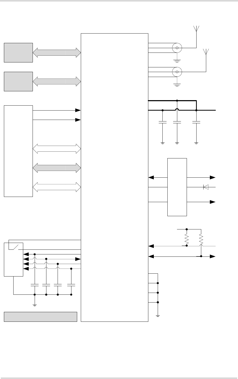
Figure 1: ELS31-US/ELS51-US system overview
GPIO
interface
I2C
USB
ASC0
ASC0
CONTROL
POWER
ANTENNA
(LTE dual band)
Module
SIM interface
(with SIM detection)
SIM card
Application
Power supply
Emergency reset
ON
Serial modem
interface
Serial modem
interface
I2C
3
4
4
5
2
1
1
2
USB
Antenna /
div. Antenna
2
GPIOs
7
Status LED
1
FST_SHDN Fast shutdown
1
1
ADC ADC
1
COUNTER Pulse counter
1
GP(I)Os
HSIC
SDIO
4
3
HSIC
SDIO
SPI SPI
3
SPI SPI
2
ASC1 Serial interface
4
Cinterion® ELS31-/ELS51-US Hardware Interface Overview
2 Interface Characteristics
29
ELS31-US_ELS51-US_HIO_v01.000a 2016-12-28
Confidential / Preliminary
Page 11 of 46
2 Interface Characteristics
ELS31-US/ELS51-US is equipped with an SMT application interface that connects to the ex-
ternal application. The SMT application interface incorporates the various application interfac-
es as well as the RF antenna interfaces.
2.1 Application Interface
2.1.1 USB Interface
ELS31-US/ELS51-US supports a USB 2.0 High Speed (480Mbit/s) device interface that is Full
Speed (12Mbit/s) compliant. The USB interface is primarily intended for use as command and
data interface and for downloading firmware.
The VUSB line is used for cable detection only, this is to be supplied by the external device. The
USB circuitry in the ELS31-US/ELS51-US is designed to meet the USB 2.0 specification for
self-power.2.0”1.
Figure 2: USB circuit
To properly connect the module's USB interface to the external application, a USB 2.0 compat-
ible connector and cable or hardware design is required. Furthermore, the USB modem driver
distributed with ELS31-US/ELS51-US needs to be installed.
1. The specification is ready for download on http://www.usb.org/developers/docs/
VBUS
DP
DN
VREG (3V075)
BATT+
USB_DP2)
lin. reg.
GND
Module
Detection only VUSB_IN
USB part1)
RING0
Host wakeup
1) It is recommended to add EMI suppression filter (see section 2.1.3.1)
USB_DN2)
2) If the USB interface is operated in High Speed mode (480MHz), it is recommended to take
special care routing the data lines USB_DP and USB_DN. Application layout should in this
case implement a differential impedance of 90Ohm for proper signal integrity.
SMT
Cinterion® ELS31-/ELS51-US Hardware Interface Overview
2.1 Application Interface
29
ELS31-US_ELS51-US_HIO_v01.000a 2016-12-28
Confidential / Preliminary
Page 12 of 46
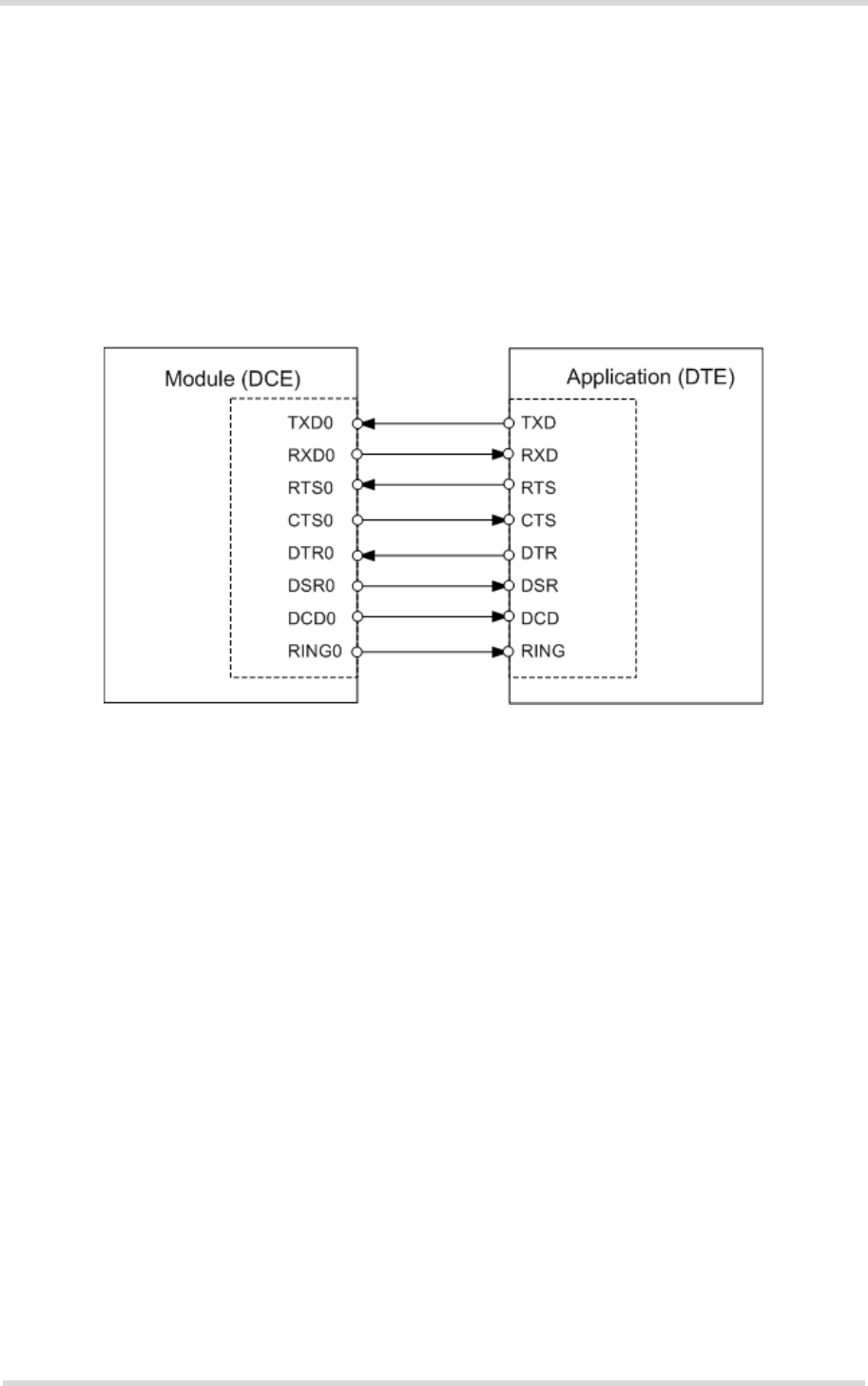
2.1.2 Serial Interface ASC0
ELS31-US/ELS51-US offers an 8-wire unbalanced, asynchronous modem interface ASC0
conforming to ITU-T V.24 protocol DCE signalling. The electrical characteristics do not comply
with ITU-T V.28. The significant levels are 0V (for low data bit or active state) and 1.8V (for high
data bit or inactive state).
ELS31-US/ELS51-US is designed for use as a DCE. Based on the conventions for DCE-DTE
connections it communicates with the customer application (DTE) using the following signals:
• Port TXD @ application sends data to the module’s TXD0 signal line
• Port RXD @ application receives data from the module’s RXD0 signal line
Figure 3: Serial interface ASC0
Features:
• Includes the data lines TXD0 and RXD0, the status lines RTS0 and CTS0 and, in addition,
the modem control lines DTR0, DSR0, DCD0 and RING0.
• Configured for 8 data bits, no parity and 1 stop bit.
• ASC0 can be operated at fixed bit rates from 4800bps up to 921600bps.
• Supports RTS0/CTS0 hardware flow control. Communication is possible by using only RXD
and TXD lines, if RTS0 is pulled low.
• Wake up from SLEEP mode by RTS0 activation.
The ASC0 interface is dedicated to signaling via AT commands (3GPP standard 27.007 + mod-
ule specific AT commands).
Cinterion® ELS31-/ELS51-US Hardware Interface Overview
2.1 Application Interface
29
ELS31-US_ELS51-US_HIO_v01.000a 2016-12-28
Confidential / Preliminary
Page 13 of 46
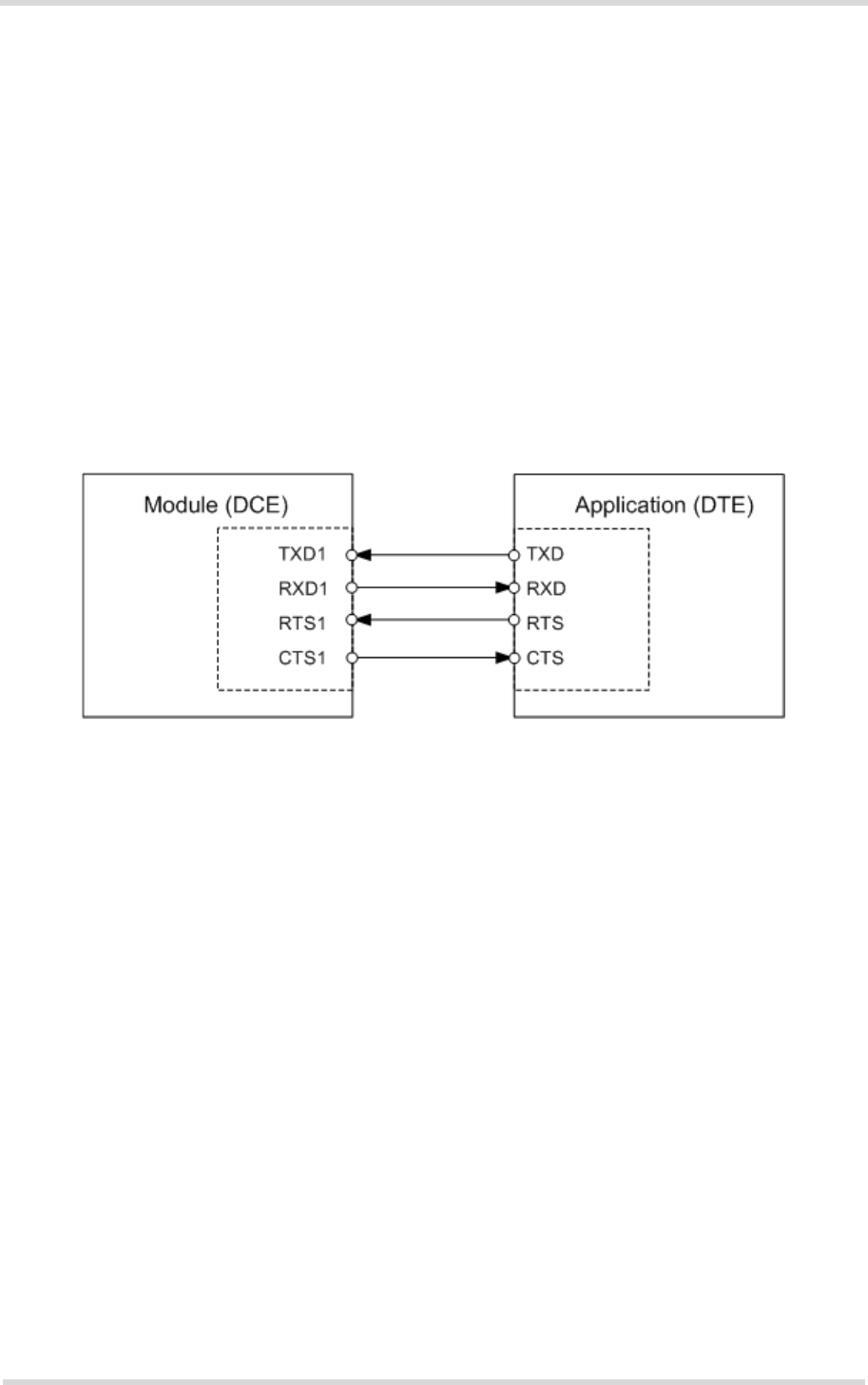
2.1.3 Serial Interface ASC1
ELS31-US/ELS51-US provides a 4-wire unbalanced, asynchronous modem interface ASC1
conforming to ITU-T V.24 protocol DCE signaling. The electrical characteristics do not comply
with ITU-T V.28. The significant levels are 0V (for low data bit or active state) and 1.8V (for high
data bit or inactive state).
The ASC1 interface lines are originally available as GPIO lines. If configured as ASC1 lines,
the GPIO lines are assigned as follows: GPIO16 --> RXD1, GPIO17 --> TXD1, GPIO18 -->
RTS1 and GPIO19 --> CTS1. Configuration is done by AT command (see [1]: AT^SCFG). The
configuration is non-volatile and becomes active after a module restart.
ELS51-US is designed for use as a DCE. Based on the conventions for DCE-DTE connections
it communicates with the customer application (DTE) using the following signals:
• Port TXD @ application sends data to module’s TXD1 signal line
• Port RXD @ application receives data from the module’s RXD1 signal line
Figure 4: Serial interface ASC1
Features
• Includes only the data lines TXD1 and RXD1 plus RTS1 and CTS1 for hardware hand-
shake.
• On ASC1 no RING line is available.
• Configured for 8 data bits, no parity and 1 or 2 stop bits.
• ASC1 can be operated at fixed bit rates from 4800 bps to 921600 bps.
• Supports RTS1/CTS1 hardware flow control. Communication is possible by using only RXD
and TXD lines, if RTS1 is pulled low.
• Wake up from SLEEP mode by RTS0 activation.
AT commands for signaling are not supported on ASC1 interface. ASC1 is intended only for
data transfer in a Linux environment.
Cinterion® ELS31-/ELS51-US Hardware Interface Overview
2.1 Application Interface
29
ELS31-US_ELS51-US_HIO_v01.000a 2016-12-28
Confidential / Preliminary
Page 14 of 46
2.1.4 UICC/SIM/USIM Interface
ELS31-US/ELS51-US has an integrated UICC/SIM/USIM interface compatible with the 3GPP
31.102 and ETSI 102 221. This is wired to the host interface in order to be connected to an
external SIM card holder. Five pads on the SMT application interface are reserved for the SIM
interface.
The UICC/SIM/USIM interface supports 3V and 1.8V SIM cards.
The CCIN signal serves to detect whether a tray (with SIM card) is present in the card holder.
The CCIN signal must be connected to V180 for the detection to work on the module. Other-
wise the SIM card can never be detected by the module.
Using the CCIN signal is mandatory for compliance with the GSM 11.11 recommendation if the
mechanical design of the host application allows the user to remove the SIM card during oper-
ation. To take advantage of this feature, an appropriate SIM card detect switch is required on
the card holder. For example, this is true for the model supplied by Molex, which has been test-
ed to operate with ELS31-US/ELS51-US and is part of the Gemalto M2M reference equipment
submitted for type approval. See Section 7.1 for Molex ordering numbers.
Note: No guarantee can be given, nor any liability accepted, if loss of data is encountered after
removing the SIM card during operation. Also, no guarantee can be given for properly initializ-
ing any SIM card that the user inserts after having removed the SIM card during operation. In
this case, the application must restart ELS31-US/ELS51-US.
Table 1: Signals of the SIM interface (SMT application interface)
Signal Description
GND Separate ground connection for SIM card to improve EMC.
CCCLK Chipcard clock
CCVCC SIM supply voltage.
CCIO Serial data line, input and output.
CCRST Chipcard reset
CCIN Input on the baseband processor for detecting a SIM card tray in the holder. If the SIM is
removed during operation the SIM interface is shut down immediately to prevent destruc-
tion of the SIM. The CCIN signal is by default low and will change to high level if a SIM card
is inserted.
The CCIN signal is mandatory for applications that allow the user to remove the SIM card
during operation.
The CCIN signal is solely intended for use with a SIM card. It must not be used for any other
purposes. Failure to comply with this requirement may invalidate the type approval of
ELS31-US/ELS51-US.
Cinterion® ELS31-/ELS51-US Hardware Interface Overview
2.1 Application Interface
29
ELS31-US_ELS51-US_HIO_v01.000a 2016-12-28
Confidential / Preliminary
Page 15 of 46
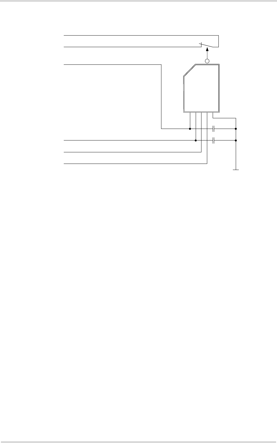
The figure below shows a circuit to connect an external SIM card holder.
Figure 5: External UICC/SIM/USIM card holder circuit
The total cable length between the SMT application interface pads on ELS31-US/ELS51-US
and the pads of the external SIM card holder must not exceed 100mm in order to meet the
specifications of 3GPP TS 51.010-1 and to satisfy the requirements of EMC compliance.
To avoid possible cross-talk from the CCCLK signal to the CCIO signal be careful that both
lines are not placed closely next to each other. A useful approach is using a GND line to shield
the CCIO line from the CCCLK line.
The ELS31-US/ELS51-US includes embedded ESD protection for the SIM interface that com-
plies to ETSI EN 301 489-1/7: Contact discharge: ± 4kV, air discharge: ± 8kV.
SIM
CCVCC
CCRST
CCIO
CCCLK
220nF
1nF
CCIN
V180
Cinterion® ELS31-/ELS51-US Hardware Interface Overview
2.1 Application Interface
29
ELS31-US_ELS51-US_HIO_v01.000a 2016-12-28
Confidential / Preliminary
Page 16 of 46
2.1.5 GPIO Interface
ELS31-US/ELS51-US offers a GPIO interface with 17 GPIO and 3 GPO lines. The lines are
shared with other interfaces or functions: Fast shutdown (see Section 2.1.11.2), status LED
(see Section 2.1.11.1), a pulse counter (see Section 2.1.8), ASC0 (see Section 2.1.2), ASC1
(see Section 2.1.3), SPI (see Section 2.1.7), and HSIC (see Section 2.1.9).
The following table shows the configuration variants for the GPIO pads. All variants are mutu-
ally exclusive, i.e. a pad configured for instance as Status LED is locked for alternative usage.
After startup, the above mentioned alternative GPIO line assignments can be configured using
AT commands (see [1]). The configuration is non-volatile and available after module restart.
Notes:
• GPO5, GPO23 and GPO26 are GPOs only.
Table 2: GPIO lines and possible alternative assignment
GPIO Fast
Shutdown Status
LED Pulse
Counter ASC0 ASC1 SPI HSIC
GPIO1 DTR0
GPIO2 DCD0
GPIO3 DSR0
GPIO4 FST_SHDN
GPO5 LED
GPIO6
GPIO7
GPIO8 COUNTER
GPIO16 RXD1 AP_WAKEUP
GPIO17 TXD1 HOST_ACTIVE
GPIO18 RTS1 CP_WAKEUP
GPIO19 CTS1 SUSPEND
GPIO20
GPIO21
GPIO22
GPO23
GPIO24 RING0
GPIO25
GPO26 SPI_CS1
GPIO27 SPI_CS2

Cinterion® ELS31-/ELS51-US Hardware Interface Overview
2.1 Application Interface
29
ELS31-US_ELS51-US_HIO_v01.000a 2016-12-28
Confidential / Preliminary
Page 17 of 46
2.1.6 I2C Interface
I2C is a serial, 8-bit oriented data transfer bus for bit rates up to 100kbps. It consists of two lines,
the serial data line I2CDAT and the serial clock line I2CCLK. The module acts as a single mas-
ter device, e.g. the clock I2CCLK is driven by the module. I2CDAT is a bi-directional line. Each
device connected to the bus is software addressable by a unique 7-bit address, and simple
master/slave relationships exist at all times. The module operates as master-transmitter or as
master-receiver. The customer application transmits or receives data only on request of the
module.
The I2C interface can be powered via the V180 line of ELS31-US/ELS51-US. If connected to
the V180 line, the I2C interface will properly shut down when the module enters the Power
Down mode.
Note: Good care should be taken when creating the PCB layout of the host application: The
traces of I2CCLK and I2CDAT should be equal in length and as short as possible.
2.1.7 SPI Interface
The ELS31-US/ELS51-US GPIO interface lines can be configured as Serial Peripheral Inter-
face (SPI). The SPI is a synchronous serial interface for control and data transfer between
ELS31-US/ELS51-US and the external application. Only one application can be connected to
the SPI and the interface supports only master mode. The transmission rates are up to 6.5Mbit/
s. The SPI interface comprises the two data lines SPI_MOSI and SPI_MISO, the clock line
SPI_CLK a well as the chip select lines SPI_CS1 and SPI_CS2.
2.1.8 Pulse Counter
The GPIO8 line can be configured as pulse counter line COUNTER (for GPIOs see Section
2.1.5). The pulse counter interface can be used, for example, as a clock - it is designed to mea-
sure signals from 0 to 1000 pulses per second. Note that the pulse counter works in batches
of 8 pulses, i.e., the URC indicates the number of pulses counted in batches of 8 pulses. For
more information on how to use this feature see [1].
2.1.9 HSIC Interface (ELS51-US Only)
The (USB) High Speed Inter Chip (HSIC) interface can be used between the module and an
external application processor, and is compliant to the High Speed USB 2.0 interface with
480Mbit/s. The maximum distance between module processor and external application proces-
sor should not exceed 100mm.
The HSIC interface comprises two signal lines (strobe - HSIC_STRB - and data - HSIC_DATA)
used in a source synchronous serial interface with a 240MHz clock to provide a 480Mbps USB
interface. The HSIC_STRB and HSIC_DATA lines are high-speed signals and should be rout-
ed as 50Ohm impedance traces. The trace length of these signals should be balanced to min-
imize timing skew and be no longer than 100mm.
The HSIC interface implementation complies with the USB HSIC standard “High-Speed Inter-
Chip USB Electrical Specification”, Version 1, September 23, 20071.
1. The USB specifications are ready for download on http://www.usb.org/developers/docs/usb20_docs/
Cinterion® ELS31-/ELS51-US Hardware Interface Overview
2.1 Application Interface
29
ELS31-US_ELS51-US_HIO_v01.000a 2016-12-28
Confidential / Preliminary
Page 18 of 46
2.1.10 SDIO Interface (ELS51-US Only)
The Secure Digital Input Output (SDIO) interface can be used to for instance connect an SD
card. The SDIO interface has the following features:
Table 4 lists the six SDIO interface lines:
Table 3: SDIO interface features
Feature Description/Value
Interface Type SDIO/SD1 (1 data line), SDIO/SD4 (4 data lines), MMC4 (4 data lines)
Voltage 1.8 V
DMA Mode SDMA / ADMA1 / ADMA2
Number of SLOTs 1
Implement DDR mode Yes
Card inserted status Yes
SDIOCLK frequency Default Mode: 23 MHz maximum
High Speed Mode: 46 MHz maximum
UHS-I Mode: 92 MHz
Max block length 2048 bytes
SDIO interrupt support Yes, support SDIO/SD1, SDIO/SD4 mode interrupts
Table 4: SDIO interface lines
Signal Direction Description
SDIOCLK Out SD master clock output to SD/MMC/SDIO device.
SDIOCMD I/O Command line.
SDIO0 I/O Data lines. Only SDIO0 carries data in 1-bit SD mode,
SDIO0..3 carry data in 4-bits mode.
SDIO interrupt is multiplexed with SDIO1.
SDIO1 I/O
SDIO2 I/O
SDIO3 I/O

Cinterion® ELS31-/ELS51-US Hardware Interface Overview
2.1 Application Interface
29
ELS31-US_ELS51-US_HIO_v01.000a 2016-12-28
Confidential / Preliminary
Page 19 of 46
2.1.11 Control Signals
2.1.11.1 Status LED
The LED line can also be configured as GPO5 line, and can be used to drive a status LED that
indicates different operating modes of the module (for GPOs see Section 2.1.5). LED and GPO
functionality are mutually exclusive.
2.1.11.2 Fast Shutdown
The GPIO4 interface line can be configured as fast shutdown signal line FST_SHDN. The con-
figured FST_SHDN line is an active low control signal. If enabled, a low impulse of 10 millisec-
onds on the FST_SHDN line starts the fast shutdown procedure.The fast shutdown procedure
still finishes any data activities on the module‘s flash file system, thus ensuring data integrity,
but the module will no longer deregister gracefully from the network.

Cinterion® ELS31-/ELS51-US Hardware Interface Overview
2.2 RF Antenna Interface
29
ELS31-US_ELS51-US_HIO_v01.000a 2016-12-28
Confidential / Preliminary
Page 20 of 46
2.2 RF Antenna Interface
The RF interface has an impedance of 50Ω. ELS31-US/ELS51-US is capable of sustaining a
total mismatch at the antenna line without any damage, even when transmitting at maximum
RF power.
The external antenna must be matched properly to achieve best performance regarding radi-
ated power, modulation accuracy and harmonic suppression. Antenna matching networks are
not included on the ELS31-US/ELS51-US module and should be placed in the host application
if the antenna does not have an impedance of 50Ω.
Regarding the return loss ELS31-US/ELS51-US provides the following values in the active
band:
Table 5: Return loss in the active band
State of module Return loss of module Recommended return loss of application
Receive > 8dB > 12dB
Transmit not applicable > 12dB

Cinterion® ELS31-/ELS51-US Hardware Interface Overview
2.2 RF Antenna Interface
29
ELS31-US_ELS51-US_HIO_v01.000a 2016-12-28
Confidential / Preliminary
Page 21 of 46
2.2.1 Antenna Installation
The antenna is connected by soldering the antenna pads (RF_OUT, pad #59 and DIV_ANT,
pad 56) its neighboring ground pads (GND, i.e., pads #55, #57, #58 and #60) directly to the
application’s PCB. The antenna pad is the antenna reference point (ARP) for ELS31-US/ELS51-
US. All RF data specified throughout this document is related to the ARP.
The distance between the antenna RF pads and its neighboring GND pads has been optimized
for best possible impedance. On the application PCB, special attention should be paid to these
3 pads, in order to prevent mismatch.
The wiring of the antenna connection line, starting from the antenna pad to the application an-
tenna should result in a 50Ω line impedance. Line width and distance to the GND plane needs
to be optimized with regard to the PCB’s layer stack. Some examples are given in Section
2.2.2.
To prevent receiver desensitization due to interferences generated by fast transients like high
speed clocks on the application PCB, it is recommended to realize the antenna connection line
using embedded Stripline rather than Micro-Stripline technology. Please see Section 2.2.2.2
for an example.
For type approval purposes, the use of a 50Ω coaxial antenna connector (U.FL-R-SMT) might
be necessary. In this case the U.FL-R-SMT connector should be placed as close as possible
to ELS31-US/ELS51-US‘s antenna pad.
Cinterion® ELS31-/ELS51-US Hardware Interface Overview
2.2 RF Antenna Interface
29
ELS31-US_ELS51-US_HIO_v01.000a 2016-12-28
Confidential / Preliminary
Page 22 of 46
2.2.2 RF Line Routing Design
2.2.2.1 RF Interface Signals Circuit Diagram Example
Figure 6 is a topology reference, and it is recommended not to deviate from this circuit for your
external application.
The RF inter-connects called RF Port 1 and RF Port 2 are examples only. Depending on the
RF antenna, the interfacing system will dictate the RF inter-connects.
Figure 6: RF interface signals example
Please be also aware of ESD protection required on the RF interface lines. ESD protection
might be utilized through the above pi-network (primarily intended for managing any additional
RF optimization needs), or by additional components in series with the pi-network illustrated
above.
Cinterion® ELS31-/ELS51-US Hardware Interface Overview
2.2 RF Antenna Interface
29
ELS31-US_ELS51-US_HIO_v01.000a 2016-12-28
Confidential / Preliminary
Page 23 of 46
2.2.2.2 Line Arrangement Examples
Several dedicated tools are available to calculate line arrangements for specific applications
and PCB materials - for example from http://www.polarinstruments.com/ (commercial software)
or from http://web.awrcorp.com/Usa/Products/Optional-Products/TX-Line/ (free software).
Embedded Stripline
This figure below shows a line arrangement example for embedded stripline with 65µm FR4
prepreg (type: 1080) and 710µm FR4 core (4-layer PCB).
Figure 7: Embedded Stripline with 65µm prepreg (1080) and 710µm core
Cinterion® ELS31-/ELS51-US Hardware Interface Overview
2.2 RF Antenna Interface
29
ELS31-US_ELS51-US_HIO_v01.000a 2016-12-28
Confidential / Preliminary
Page 24 of 46
Micro-Stripline
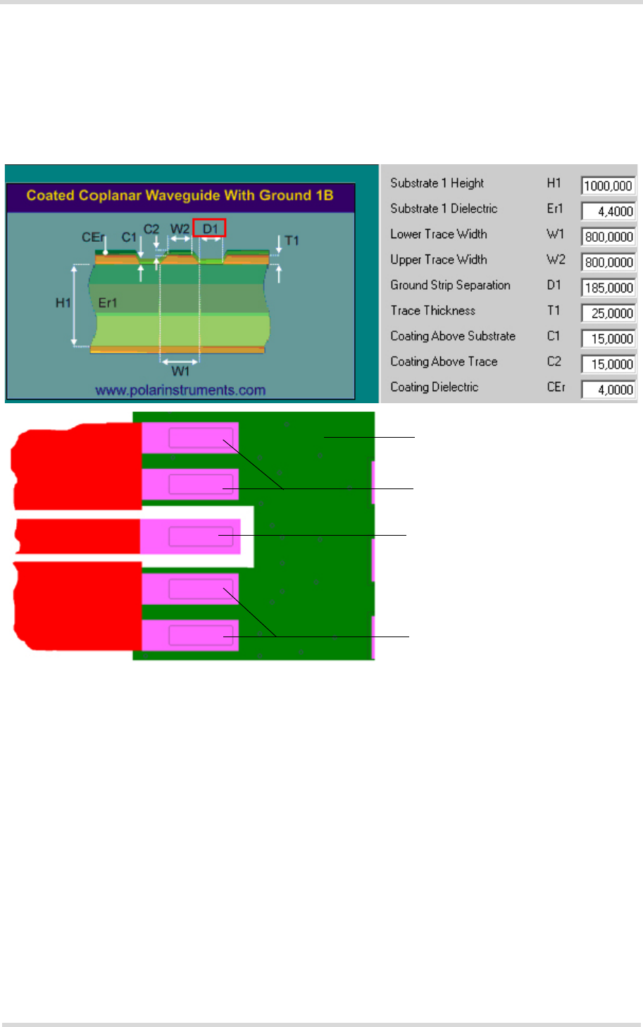
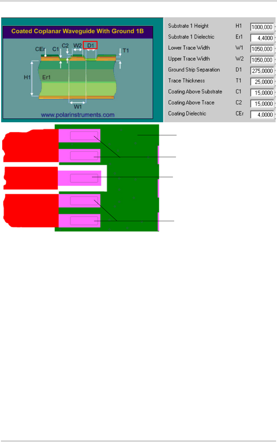
This section gives two line arrangement examples for micro-stripline.
• Micro-Stripline on 1.0mm Standard FR4 2-Layer PCB
The following two figures show examples with different values for D1 (ground strip separa-
tion).
Figure 8: Micro-Stripline on 1.0mm standard FR4 2-layer PCB - example 1
Antenna line
Ground line
Ground line
Application board
Cinterion® ELS31-/ELS51-US Hardware Interface Overview
2.2 RF Antenna Interface
29
ELS31-US_ELS51-US_HIO_v01.000a 2016-12-28
Confidential / Preliminary
Page 25 of 46
Figure 9: Micro-Stripline on 1.0mm Standard FR4 PCB - example 2
Antenna line
Ground line
Ground line
Application board
Cinterion® ELS31-/ELS51-US Hardware Interface Overview
2.2 RF Antenna Interface
29
ELS31-US_ELS51-US_HIO_v01.000a 2016-12-28
Confidential / Preliminary
Page 26 of 46
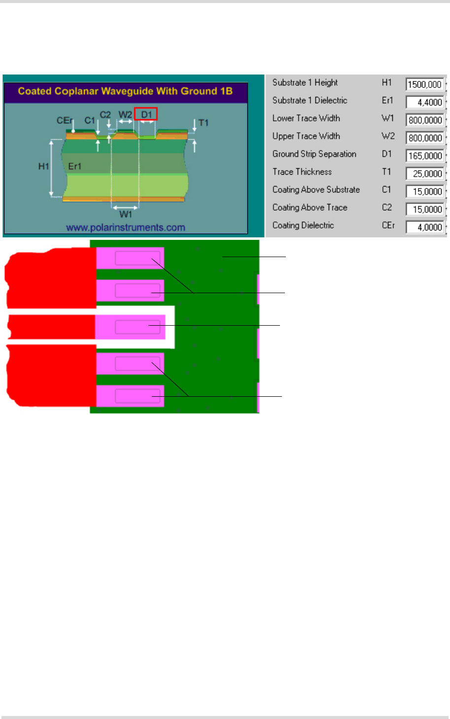
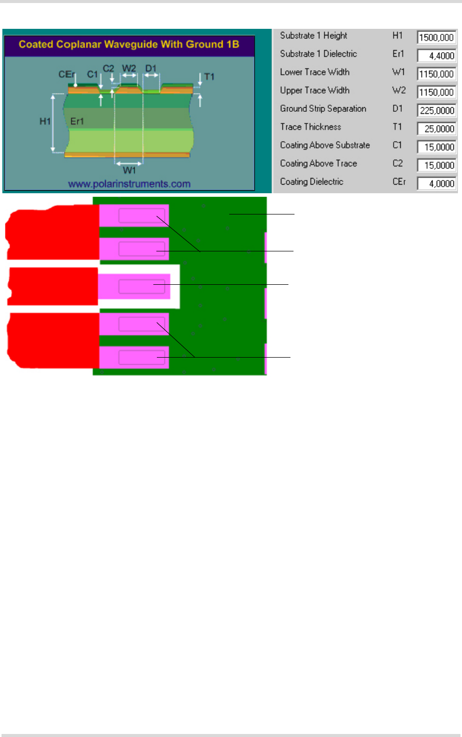
• Micro-Stripline on 1.5mm Standard FR4 2-Layer PCB
The following two figures show examples with different values for D1 (ground strip separa-
tion).
Figure 10: Micro-Stripline on 1.5mm Standard FR4 PCB - example 1
Antenna line
Ground line
Ground line
Application board
Cinterion® ELS31-/ELS51-US Hardware Interface Overview
2.2 RF Antenna Interface
29
ELS31-US_ELS51-US_HIO_v01.000a 2016-12-28
Confidential / Preliminary
Page 27 of 46
Figure 11: Micro-Stripline on 1.5mm Standard FR4 PCB - example 2
Antenna line
Ground line
Ground line
Application board

Cinterion® ELS31-/ELS51-US Hardware Interface Overview
2.3 Sample Application
29
ELS31-US_ELS51-US_HIO_v01.000a 2016-12-28
Confidential / Preliminary
Page 28 of 46
2.3 Sample Application
Figure 12 shows a typical example of how to integrate a ELS31-US/ELS51-US module with an
application. Usage of the various host interfaces depends on the desired features of the appli-
cation.
Because of the high RF field density inside the module, it cannot be guaranteed that no self
interference might occur, depending on frequency and the applications grounding concept. The
potential interferers may be minimized by placing small capacitors (47pF) at suspected lines
(e.g. RXD0, or ON).
While developing SMT applications it is strongly recommended to provide test points
for certain signals, i.e., lines to and from the module - for debug and/or test purposes.
The SMT application should allow for an easy access to these signals. For details on
how to implement test points see [4].
The EMC measures are best practice recommendations. In fact, an adequate EMC strategy for
an individual application is very much determined by the overall layout and, especially, the po-
sition of components. For example, mounting the internal acoustic transducers directly on the
PCB eliminates the need to use the ferrite beads shown in the sample schematic.
Note: ELS31-US/ELS51-US is not intended for use with cables longer than 3m.
Disclaimer
No warranty, either stated or implied, is provided on the sample schematic diagram shown in
Figure 12 and the information detailed in this section. As functionality and compliance with na-
tional regulations depend to a great amount on the used electronic components and the indi-
vidual application layout manufacturers are required to ensure adequate design and operating
safeguards for their products using ELS31-US/ELS51-US modules.
Cinterion® ELS31-/ELS51-US Hardware Interface Overview
2.3 Sample Application
29
ELS31-US_ELS51-US_HIO_v01.000a 2016-12-28
Confidential / Preliminary
Page 29 of 46
Figure 12: Schematic diagram of ELS31-US/ELS51-US sample application
ELS31/ELS51
Main Antenna
Div. Antenna
BATT+RF
BATT+BB
GPIOs
LED
COUNTER
I2CCLK
I2CDAT
GND
SDIO
HSIC
ON
FST_SHUTDOWN
ASC0
ASC1
USB
V180
CCIN
CCVCC
CCIO
CCRST
CCCLK
Power Supply
33pF 33pF + 150µF
Low ESR!
2k2 2k2
V180
Blocking
WiFi
µC
1nF 10pF10pF220nF
SIM
USB
Interfaces available only on ELS51

Cinterion® ELS31-/ELS51-US Hardware Interface Overview
3 Operating Characteristics
30
ELS31-US_ELS51-US_HIO_v01.000a 2016-12-28
Confidential / Preliminary
Page 30 of 46
3 Operating Characteristics
3.1 Operating Modes
The table below briefly summarizes the various operating modes referred to throughout the
document.
3.2 Power Supply
ELS31-US/ELS51-US needs to be connected to a power supply at the SMT application inter-
face - 2 BATT lines and GND. There are two separate voltage domains for BATT:
• BATT_BB with a line mainly for the baseband power supply.
• BATT_RF with a line for the RF power amplifier supply.
Please note that throughout the document BATT refers to both voltage domains and power
supply lines - BATT_BB and BATT_RF.
The power supply of ELS31-US/ELS51-US has to be a single voltage source at BATT_BB and
BATT_RF. It must be able to provide the current for all operation modes of the module.
All the key functions for supplying power to the device are handled by the power management
section of the analog controller. This IC provides the following features:
• Stabilizes the supply voltages for the baseband using low drop linear voltage regulators and
a DC-DC step down switching regulator.
• Switches the module's power voltages for the power-up and -down procedures.
• SIM switch to provide SIM power supply.
Table 6: Overview of operating modes
Mode Function
Normal
opera-
tion
LTE IDLE No data transfer is in progress and the USB connection is suspended
by host (or is not present) and no active communication via ASC0/
ASC1. In IDLE mode, the software can be active or in SLEEP state.
LTE DATA LTE data transfer in progress. Power consumption depends on network
settings and data transfer rate.
Power
Down
Normal shutdown after sending the power down command. Software is not active. Inter-
faces are not accessible. Operating voltage remains applied.
Airplane
mode
Airplane mode shuts down the radio part of the module, causes the module to log off from
the LTE network and disables all AT commands whose execution requires a radio connec-
tion.
Airplane mode can be controlled by AT command (see [1]).
In Airplane mode, the software can be active or in SLEEP state.
Cinterion® ELS31-/ELS51-US Hardware Interface Overview
4 Mechanical Dimensions, Mounting and Packaging
32
ELS31-US_ELS51-US_HIO_v01.000a 2016-12-28
Confidential / Preliminary
Page 31 of 46
4 Mechanical Dimensions, Mounting and Packaging
The following sections describe the mechanical dimensions of ELS31-US/ELS51-US and give
recommendations for integrating ELS31-US/ELS51-US into the host application.
4.1 Mechanical Dimensions of ELS31-US/ELS51-US
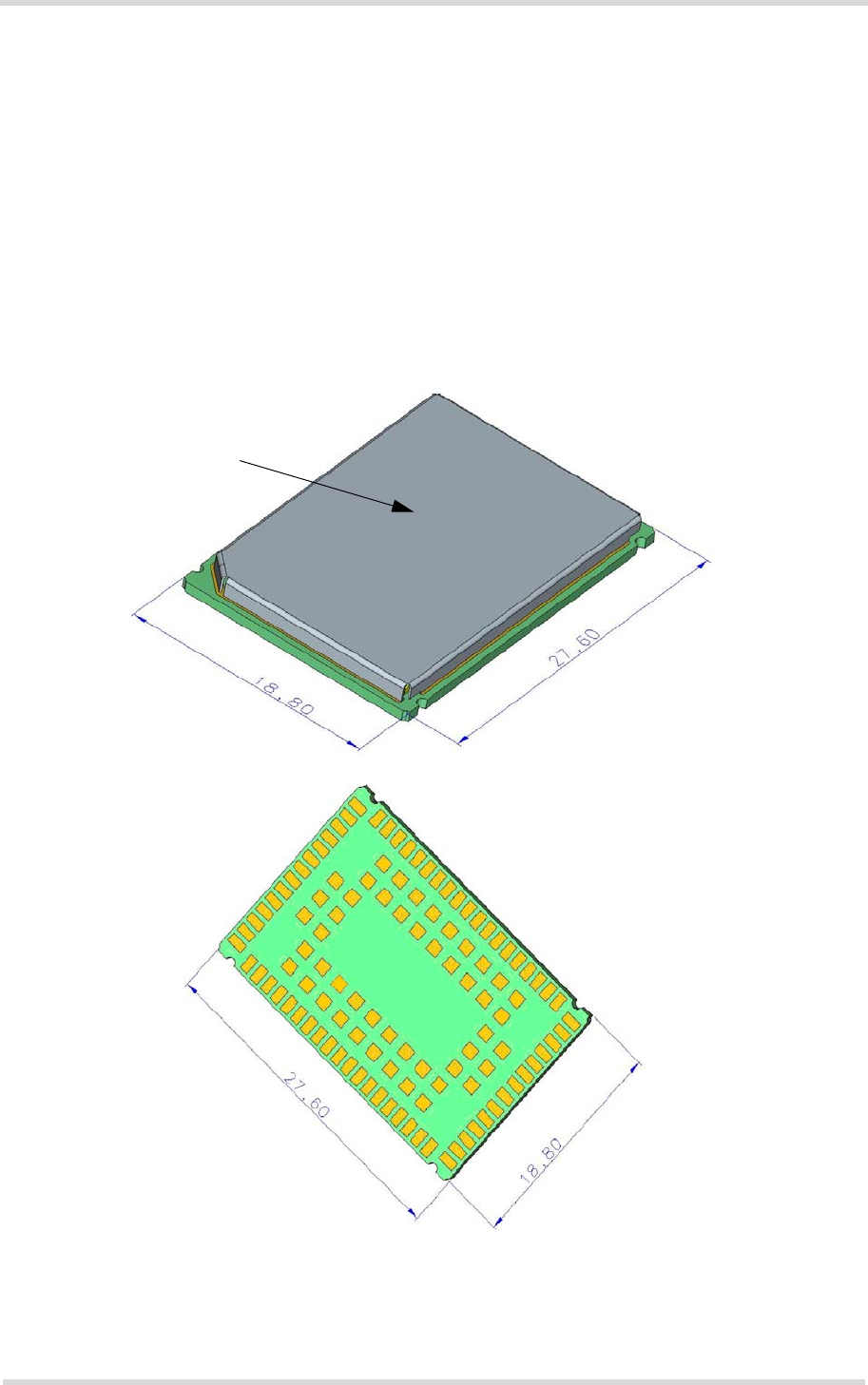
Figure 13 shows the top and bottom view of ELS31-US/ELS51-US and provides an overview
of the board's mechanical dimensions. For further details see Figure 14.
Figure 13: ELS31-US/ELS51-US– top and bottom view
Product label
Top view
Bottom view
Cinterion® ELS31-/ELS51-US Hardware Interface Overview
4.1 Mechanical Dimensions of ELS31-US/ELS51-US
32
ELS31-US_ELS51-US_HIO_v01.000a 2016-12-28
Confidential / Preliminary
Page 32 of 46
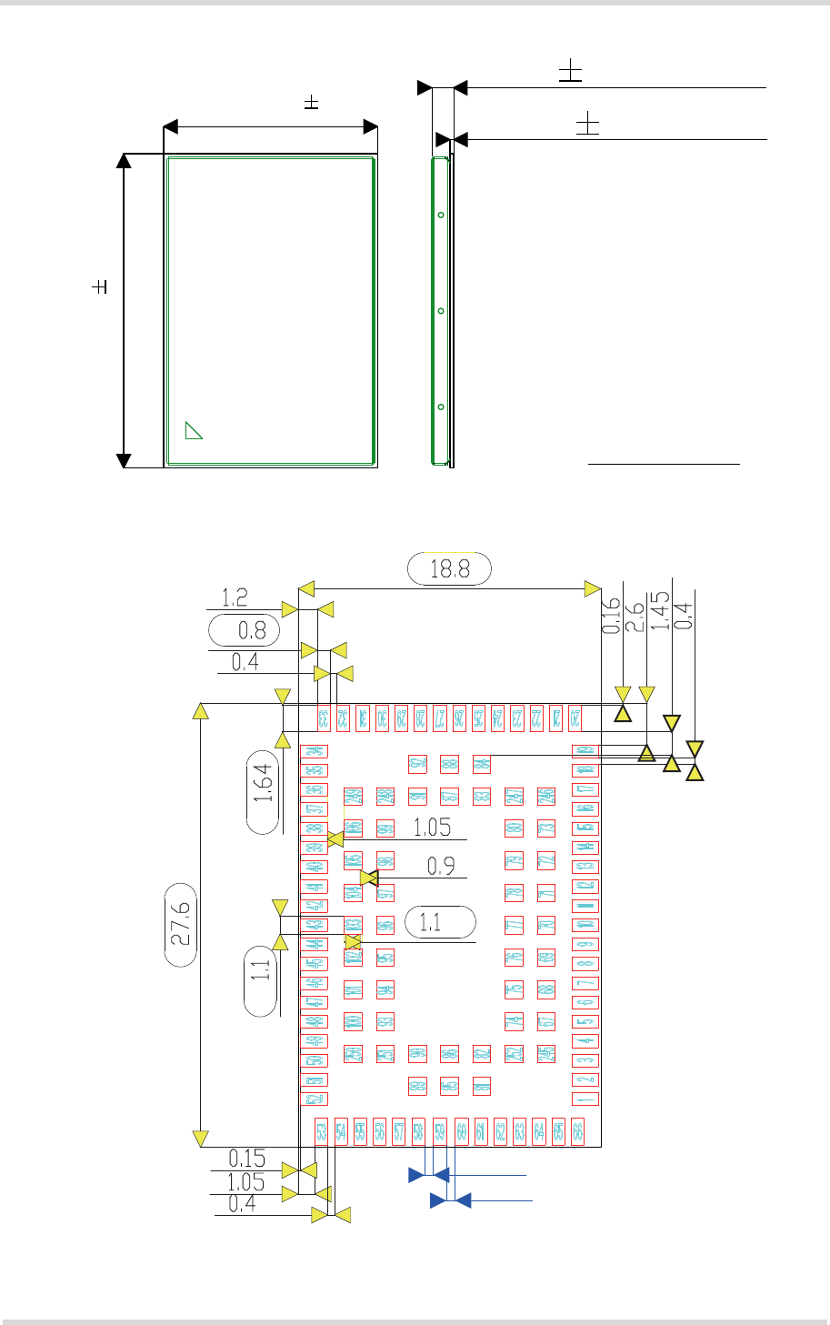
Figure 14: Dimensions of ELS31-US/ELS51-US (all dimensions in mm)
Figure 15: Dimensions of ELS31-US/ELS51-US (all dimensions in mm) - bottom view
0.1
18.8
0.1
27.6
0.31 0.04(PCB)
2.05 0.1(TOTAL)
TOP VIEW
18.8
27.6
0.8
1.2
0.4
0.55
0.55
1.05
0.4
2.6
0.4
1.45
1.05
0.15
1.64
0.9
1.1
1.1
0.16
#0550.7*&8
Cinterion® ELS31-/ELS51-US Hardware Interface Overview
5 Regulatory and Type Approval Information
38
ELS31-US_ELS51-US_HIO_v01.000a 2016-12-28
Confidential / Preliminary
Page 33 of 46
5 Regulatory and Type Approval Information
5.1 Directives and Standards
ELS31-US/ELS51-US is designed to comply with the directives and standards listed below.
It is the responsibility of the application manufacturer to ensure compliance of the final product
with all provisions of the applicable directives and standards as well as with the technical spec-
ifications provided in the "ELS31-US/ELS51-US Hardware Interface Description".
Table 7: Directives
2002/95/EC (RoHS 1)
2011/65/EC (RoHS 2)
Directive of the European Parliament and of the Council
of 27 January 2003 (and revised on 8 June 2011) on the
restriction of the use of certain hazardous substances in
electrical and electronic equipment (RoHS)
Table 8: Standards of North American type approval
CFR Title 47 Code of Federal Regulations, Part 22 and Part 24 (Telecommunications,
PCS); US Equipment Authorization FCC
OET Bulletin 65
(Edition 97-01)
Evaluating Compliance with FCC Guidelines for Human Exposure to
Radiofrequency Electromagnetic Fields
UL 60 950-1 Product Safety Certification (Safety requirements)
California Leadfree Man-
date
Covered by European RoHS requirements
RSS132 (Issue2)
RSS133 (Issue5)
Canadian Standard
Table 9: Standards of GCF type approval
3GPP TS 51.010-1 Digital cellular telecommunications system (Release 10); Mobile Station
(MS) conformance specification;
GCF-CC V3.58 Global Certification Forum - Certification Criteria
Table 10: Requirements of quality
IEC 60068 Environmental testing
DIN EN 60529 IP codes
Cinterion® ELS31-/ELS51-US Hardware Interface Overview
5.1 Directives and Standards
38
ELS31-US_ELS51-US_HIO_v01.000a 2016-12-28
Confidential / Preliminary
Page 34 of 46
Table 12: Toxic or hazardous substances or elements with defined concentration limits
Table 11: Standards of the Ministry of Information Industry of the People’s Republic of China
SJ/T 11363-2006 “Requirements for Concentration Limits for Certain Hazardous Sub-
stances in Electronic Information Products” (2006-06).
SJ/T 11364-2006 “Marking for Control of Pollution Caused by Electronic
Information Products” (2006-06).
According to the “Chinese Administration on the Control
of Pollution caused by Electronic Information Products”
(ACPEIP) the EPUP, i.e., Environmental Protection Use
Period, of this product is 20 years as per the symbol
shown here, unless otherwise marked. The EPUP is valid only as long as
the product is operated within the operating limits described in the
Gemalto M2M Hardware Interface Description.
Please see Table 12 for an overview of toxic or hazardous substances or
elements that might be contained in product parts in concentrations
above the limits defined by SJ/T 11363-2006.

Cinterion® ELS31-/ELS51-US Hardware Interface Overview
5.2 SAR requirements specific to portable mobiles
38
ELS31-US_ELS51-US_HIO_v01.000a 2016-12-28
Confidential / Preliminary
Page 35 of 46
5.2 SAR requirements specific to portable mobiles
Mobile phones, PDAs or other portable transmitters and receivers incorporating a GSM module
must be in accordance with the guidelines for human exposure to radio frequency energy. This
requires the Specific Absorption Rate (SAR) of portable ELS31-US/ELS51-US based applica-
tions to be evaluated and approved for compliance with national and/or international regula-
tions.
Since the SAR value varies significantly with the individual product design manufacturers are
advised to submit their product for approval if designed for portable use. For US markets the
relevant directives are mentioned below. It is the responsibility of the manufacturer of the final
product to verify whether or not further standards, recommendations or directives are in force
outside these areas.
Products intended for sale on US markets
ES 59005/ANSI C95.1 Considerations for evaluation of human exposure to Electromagnetic
Fields (EMFs) from Mobile Telecommunication Equipment (MTE) in the
frequency range 30MHz - 6GHz
Please note that SAR requirements are specific only for portable devices and not for mobile
devices as defined below:
• Portable device:
A portable device is defined as a transmitting device designed to be used so that the radi-
ating structure(s) of the device is/are within 20 centimeters of the body of the user.
• Mobile device:
A mobile device is defined as a transmitting device designed to be used in other than fixed
locations and to generally be used in such a way that a separation distance of at least 20
centimeters is normally maintained between the transmitter's radiating structure(s) and the
body of the user or nearby persons. In this context, the term ''fixed location'' means that the
device is physically secured at one location and is not able to be easily moved to another
location.
Cinterion® ELS31-/ELS51-US Hardware Interface Overview
5.3 Reference Equipment for Type Approval
38
ELS31-US_ELS51-US_HIO_v01.000a 2016-12-28
Confidential / Preliminary
Page 36 of 46
5.3 Reference Equipment for Type Approval
The Gemalto M2M reference setup submitted to type approve ELS31-US/ELS51-US (including
a special approval adapter for the DSB75) is shown in the following figure1:
Figure 16: Reference equipment for Type Approval
1. For RF performance tests a mini-SMT/U.FL to SMA adapter with attached 6dB coaxial attenuator is cho-
sen to connect the evaluation module directly to the GSM/UMTS test equipment instead of employing
the SMA antenna connectors on the ELS31-US/ELS51-US-DSB75 adapter as shown in Figure 16. The
following products are recommended:
Hirose SMA-Jack/U.FL-Plug conversion adapter HRMJ-U.FLP(40)
(for details see see http://www.hirose-connectors.com/ or http://www.farnell.com/
Aeroflex Weinschel Fixed Coaxial Attenuator Model 3T/4T
(for details see http://www.aeroflex.com/ams/weinschel/pdfiles/wmod3&4T.pdf)
Antenna
GSM / GPRS / UMTS
Antenna with 1m cable
ASC0
PC
Power
supply
LTE
Base station
DSB75
ASC1
USB
Approval adapter for
DSB75
SMA
Evaluation module
ELS31
ELS51
USB
Evaluation module
ELS31
ELS51
SIM card
Top view
Bottom view
Cinterion® ELS31-/ELS51-US Hardware Interface Overview
5.4 Compliance with FCC and IC Rules and Regulations
38
ELS31-US_ELS51-US_HIO_v01.000a 2016-12-28
Confidential / Preliminary
Page 37 of 46
5.4 Compliance with FCC and IC Rules and Regulations
The Equipment Authorization Certification for the Gemalto M2M reference application de-
scribed in Section 5.3 will be registered under the following identifiers:
• ELS31-US:
FCC Identifier: QIPELS31-US
Industry Canada Certification Number: 7830A-ELS31US
Granted to Gemalto M2M GmbH
• ELS51-US:
FCC Identifier: QIPELS51-US (not yet granted)
Industry Canada Certification Number: 7830A-ELS51US (not yet granted)
Granted to Gemalto M2M GmbH
Manufacturers of mobile or fixed devices incorporating ELS31-US/ELS51-US modules are au-
thorized to use the FCC Grants and Industry Canada Certificates of the ELS31-US/ELS51-US
modules for their own final products according to the conditions referenced in these docu-
ments. In this case, an FCC/ IC label of the module shall be visible from the outside, or the host
device shall bear a second label stating "Contains FCC ID: QIPELS31-US" / "Contains FCC ID:
QIPELS51-US", and accordingly “Contains IC: 7830A-ELS31US“ / “Contains IC: 7830A-
ELS51US“. The integration is limited to fixed or mobile categorized host devices, where a sep-
aration distance between the antenna and any person of min. 20cm can be assured during nor-
mal operating conditions.
For mobile and fixed operation configurations the antenna gain, including cable loss, must not
exceed the limits in the following Table 9 for FCC and IC.
IMPORTANT:
Manufacturers of portable applications incorporating ELS31-US/ELS51-US modules are re-
quired to have their final product certified and apply for their own FCC Grant and Industry Can-
ada Certificate related to the specific portable mobile. This is mandatory to meet the SAR
requirements for portable mobiles (see Section 5.2 for detail).
Changes or modifications not expressly approved by the party responsible for compliance
could void the user's authority to operate the equipment.
Note: This equipment has been tested and found to comply with the limits for a Class B digital
device, pursuant to part 15 of the FCC Rules and with Industry Canada license-exempt RSS
standard(s). These limits are designed to provide reasonable protection against harmful inter-
ference in a residential installation. This equipment generates, uses and can radiate radio fre-
Table 13: Antenna gain limits for FCC and IC (TBD)
Operating band FCC limit IC limit Unit
Maximum gain in lower operating bands with f< 1GHz
(LTE Bd12)
8.72 6.10 dBi
Maximum gain in higher operating bands with f=1700MHz
(LTE Bd4)
5.00 5.00 dBi
Maximum gain in higher operating bands with f=1900MHz
(LTE Bd2)
8.01 8.01 dBi

Cinterion® ELS31-/ELS51-US Hardware Interface Overview
5.4 Compliance with FCC and IC Rules and Regulations
38
ELS31-US_ELS51-US_HIO_v01.000a 2016-12-28
Confidential / Preliminary
Page 38 of 46
quency energy and, if not installed and used in accordance with the instructions, may cause
harmful interference to radio communications. However, there is no guarantee that interference
will not occur in a particular installation. If this equipment does cause harmful interference to
radio or television reception, which can be determined by turning the equipment off and on, the
user is encouraged to try to correct the interference by one or more of the following measures:
• Reorient or relocate the receiving antenna.
• Increase the separation between the equipment and receiver.
• Connect the equipment into an outlet on a circuit different from that to which the receiver is
connected.
• Consult the dealer or an experienced radio/TV technician for help.
This Class B digital apparatus complies with Canadian ICES-003.
If Canadian approval is requested for devices incorporating ELS31US / ELS51-US modules the
above note will have to be provided in the English and French language in the final user docu-
mentation. Manufacturers/OEM Integrators must ensure that the final user documentation does
not contain any information on how to install or remove the module from the final product.
Notes (IC):
(EN) This Class B digital apparatus complies with Canadian ICES-003 and RSS-210. Opera-
tion is subject to the following two conditions: (1) this device may not cause interference, and
(2) this device must accept any interference, including interference that may cause undesired
operation of the device.
(FR) Cet appareil numérique de classe B est conforme aux normes canadiennes ICES-003 et
RSS-210. Son fonctionnement est soumis aux deux conditions suivantes: (1) cet appareil ne
doit pas causer d'interférence et (2) cet appareil doit accepter toute interférence, notamment
les interférences qui peuvent affecter son fonctionnement.
(EN) Radio frequency (RF) Exposure Information
The radiated output power of the Wireless Device is below the Industry Canada (IC) radio fre-
quency exposure limits. The Wireless Device should be used in such a manner such that the
potential for human contact during normal operation is minimized.
This device has also been evaluated and shown compliant with the IC RF Exposure limits un-
der mobile exposure conditions (antennas at least 20cm from a person‘s body).
(FR) Informations concernant l'exposltion aux fréquences radio (RF)
La puissance de sortie émise par l'appareil de sans fiI est inférieure à la limite d'exposition aux
fréquences radio d‘Industry Canada (IC). Utilisez l'appareil de sans fil de façon à minimiser les
contacts humains lors du fonctionnement normal.
Ce périphérique a également été évalué et démontré conforme aux limites d'exposition aux RF
d'IC dans des conditions d'exposition à des appareils mobiles (les antennes se situent à moins
de 20cm du corps d'une personne).
Cinterion® ELS31-/ELS51-US Hardware Interface Overview
6 Document Information
43
ELS31-US_ELS51-US_HIO_v01.000a 2016-12-28
Confidential / Preliminary
Page 39 of 46
6 Document Information
6.1 Revision History
New document: "Cinterion® ELS31-/ELS51-US Hardware Interface Overview" v01.000a
6.2 Related Documents
[1] ELS31-US/ELS51-US AT Command Set
[2] ELS31-US/ELS51-US Release Note
[3] Application Note 40: Thermal Solutions
[4] Application Note 48: SMT Module Integration
[5] Universal Serial Bus Specification Revision 2.0, April 27, 2000
6.3 Terms and Abbreviations
Chapter What is new
-- Initial document setup.
Abbreviation Description
ADC Analog-to-digital converter
AGC Automatic Gain Control
ANSI American National Standards Institute
ARFCN Absolute Radio Frequency Channel Number
ARP Antenna Reference Point
ASC0/ASC1 Asynchronous Controller. Abbreviations used for first and second serial interface of
the module
B Thermistor Constant
BER Bit Error Rate
BTS Base Transceiver Station
CB or CBM Cell Broadcast Message
CE Conformité Européene (European Conformity)
CHAP Challenge Handshake Authentication Protocol
CPU Central Processing Unit
CS Coding Scheme
CSD Circuit Switched Data
CTS Clear to Send
DAC Digital-to-Analog Converter
DAI Digital Audio Interface

Cinterion® ELS31-/ELS51-US Hardware Interface Overview
6.3 Terms and Abbreviations
43
ELS31-US_ELS51-US_HIO_v01.000a 2016-12-28
Confidential / Preliminary
Page 40 of 46
dBm0 Digital level, 3.14dBm0 corresponds to full scale, see ITU G.711, A-law
DCE Data Communication Equipment (typically modems, e.g. Gemalto M2M module)
DCS 1800 Digital Cellular System, also referred to as PCN
DRX Discontinuous Reception
DSB Development Support Box
DSP Digital Signal Processor
DSR Data Set Ready
DTE Data Terminal Equipment (typically computer, terminal, printer or, for example, GSM
application)
DTR Data Terminal Ready
DTX Discontinuous Transmission
EFR Enhanced Full Rate
EGSM Enhanced GSM
EIRP Equivalent Isotropic Radiated Power
EMC Electromagnetic Compatibility
ERP Effective Radiated Power
ESD Electrostatic Discharge
ETS European Telecommunication Standard
FCC Federal Communications Commission (U.S.)
FDMA Frequency Division Multiple Access
FR Full Rate
GMSK Gaussian Minimum Shift Keying
GPIO General Purpose Input/Output
GPRS General Packet Radio Service
GSM Global Standard for Mobile Communications
HiZ High Impedance
HR Half Rate
HSIC High-Speed Inter-Chip
I/O Input/Output
IC Integrated Circuit
IMEI International Mobile Equipment Identity
ISO International Standards Organization
ITU International Telecommunications Union
kbps kbits per second
LED Light Emitting Diode
Li-Ion/Li+ Lithium-Ion
Li battery Rechargeable Lithium Ion or Lithium Polymer battery
LTE Long Term Evolution
Abbreviation Description

Cinterion® ELS31-/ELS51-US Hardware Interface Overview
6.3 Terms and Abbreviations
43
ELS31-US_ELS51-US_HIO_v01.000a 2016-12-28
Confidential / Preliminary
Page 41 of 46
Mbps Mbits per second
MMI Man Machine Interface
MO Mobile Originated
MS Mobile Station (GSM module), also referred to as TE
MSISDN Mobile Station International ISDN number
MT Mobile Terminated
NTC Negative Temperature Coefficient
OEM Original Equipment Manufacturer
PA Power Amplifier
PAP Password Authentication Protocol
PBCCH Packet Switched Broadcast Control Channel
PCB Printed Circuit Board
PCL Power Control Level
PCM Pulse Code Modulation
PCN Personal Communications Network, also referred to as DCS 1800
PCS Personal Communication System, also referred to as GSM 1900
PLL Phase Locked Loop
PPP Point-to-point protocol
PSK Phase Shift Keying
PSU Power Supply Unit
R&TTE Radio and Telecommunication Terminal Equipment
RAM Random Access Memory
RF Radio Frequency
RLS Radio Link Stability
RoHS Restriction of the use of certain hazardous substances in electrical and electronic
equipment.
RTS Request to Send
Rx Receive Direction
SAR Specific Absorption Rate
SAW Surface Acoustic Wave
SDIO Secure Digital Input Output
SELV Safety Extra Low Voltage
SIM Subscriber Identification Module
SMD Surface Mount Device
SMS Short Message Service
SMT Surface Mount Technology
SRAM Static Random Access Memory
TA Terminal adapter (e.g. GSM module)
Abbreviation Description

Cinterion® ELS31-/ELS51-US Hardware Interface Overview
6.3 Terms and Abbreviations
43
ELS31-US_ELS51-US_HIO_v01.000a 2016-12-28
Confidential / Preliminary
Page 42 of 46
TDMA Time Division Multiple Access
TE Terminal Equipment, also referred to as DTE
TLS Transport Layer Security
Tx Transmit Direction
UART Universal asynchronous receiver-transmitter
URC Unsolicited Result Code
USSD Unstructured Supplementary Service Data
VSWR Voltage Standing Wave Ratio
Abbreviation Description
Cinterion® ELS31-/ELS51-US Hardware Interface Overview
6.4 Safety Precaution Notes
43
ELS31-US_ELS51-US_HIO_v01.000a 2016-12-28
Confidential / Preliminary
Page 43 of 46
6.4 Safety Precaution Notes
The following safety precautions must be observed during all phases of the operation, usage,
service or repair of any cellular terminal or mobile incorporating ELS31-US/ELS51-US. Manu-
facturers of the cellular terminal are advised to convey the following safety information to users
and operating personnel and to incorporate these guidelines into all manuals supplied with the
product. Failure to comply with these precautions violates safety standards of design, manu-
facture and intended use of the product. Gemalto M2M assumes no liability for customer’s fail-
ure to comply with these precautions.
When in a hospital or other health care facility, observe the restrictions on the use of
mobiles. Switch the cellular terminal or mobile off, if instructed to do so by the guide-
lines posted in sensitive areas. Medical equipment may be sensitive to RF energy.
The operation of cardiac pacemakers, other implanted medical equipment and hear-
ing aids can be affected by interference from cellular terminals or mobiles placed close
to the device. If in doubt about potential danger, contact the physician or the manufac-
turer of the device to verify that the equipment is properly shielded. Pacemaker
patients are advised to keep their hand-held mobile away from the pacemaker, while
it is on.
Switch off the cellular terminal or mobile before boarding an aircraft. Make sure it can-
not be switched on inadvertently. The operation of wireless appliances in an aircraft is
forbidden to prevent interference with communications systems. Failure to observe
these instructions may lead to the suspension or denial of cellular services to the
offender, legal action, or both.
Do not operate the cellular terminal or mobile in the presence of flammable gases or
fumes. Switch off the cellular terminal when you are near petrol stations, fuel depots,
chemical plants or where blasting operations are in progress. Operation of any elec-
trical equipment in potentially explosive atmospheres can constitute a safety hazard.
Your cellular terminal or mobile receives and transmits radio frequency energy while
switched on. Remember that interference can occur if it is used close to TV sets,
radios, computers or inadequately shielded equipment. Follow any special regulations
and always switch off the cellular terminal or mobile wherever forbidden, or when you
suspect that it may cause interference or danger.
Road safety comes first! Do not use a hand-held cellular terminal or mobile when driv-
ing a vehicle, unless it is securely mounted in a holder for speakerphone operation.
Before making a call with a hand-held terminal or mobile, park the vehicle.
Speakerphones must be installed by qualified personnel. Faulty installation or opera-
tion can constitute a safety hazard.
IMPORTANT!
Cellular terminals or mobiles operate using radio signals and cellular networks.
Because of this, connection cannot be guaranteed at all times under all conditions.
Therefore, you should never rely solely upon any wireless device for essential com-
munications, for example emergency calls.
Remember, in order to make or receive calls, the cellular terminal or mobile must be
switched on and in a service area with adequate cellular signal strength.
Some networks do not allow for emergency calls if certain network services or phone
features are in use (e.g. lock functions, fixed dialing etc.). You may need to deactivate
those features before you can make an emergency call.
Some networks require that a valid SIM card be properly inserted in the cellular termi-
nal or mobile.
Cinterion® ELS31-/ELS51-US Hardware Interface Overview
7 Appendix
45
ELS31-US_ELS51-US_HIO_v01.000a 2016-12-28
Confidential / Preliminary
Page 44 of 46
7 Appendix
7.1 List of Parts and Accessories
Table 14: List of parts and accessories
Description Supplier Ordering information
ELS31-US Gemalto M2M Standard module
Gemalto M2M IMEI:
Packaging unit (ordering) number:
L30960-N4520-A200
Module label number:
S30960-S4520-A200-11
Customer IMEI module
Packaging unit (ordering) number:
L30960-N4525-A200
Module label number:
S30960-S4520-A200-11
1. Note: At the discretion of Gemalto M2M, module label information can either be laser engraved on the
module’s shielding or be printed on a label adhered to the module’s shielding.
ELS51-US Gemalto M2M Standard module
Gemalto M2M IMEI:
Packaging unit (ordering) number:
L30960-N4550-A200
Module label number:
S30960-S4550-A200-11
Customer IMEI module
Packaging unit (ordering) number:
L30960-N4555-A200
Module label number:
S30960-S4555-A200-11
ELS31-US Evaluation Mod-
ule
Gemalto M2M Ordering number:
L30960-N4521-A200
ELS51-US Evaluation Mod-
ule
Gemalto M2M Ordering number:
L30960-N4551-A200
DSB75 Evaluation Kit Gemalto M2M Ordering number: L36880-N8811-A100
DSB Mini
Compact Evaluation Board
Gemalto M2M Ordering number: L30960-N0030-A100
Starter Kit B80 Gemalto M2M Ordering Number L30960-N0040-A100
Multi-Adapter R1 for mount-
ing ELS31-US/ELS51-US
evaluation modules onto
DSB75
Gemalto M2M Ordering number: L30960-N0010-A100
Approval adapter for mount-
ing ELS31-US/ELS51-US
evaluation modules onto
DSB75
Gemalto M2M Ordering number: L30960-N2301-A100
SIM card holder incl. push
button ejector and slide-in
tray
Molex Ordering numbers: 91228
91236
Sales contacts are listed in Table 15.

Cinterion® ELS31-/ELS51-US Hardware Interface Overview
7.1 List of Parts and Accessories
45
ELS31-US_ELS51-US_HIO_v01.000a 2016-12-28
Confidential / Preliminary
Page 45 of 46
Table 15: Molex sales contacts (subject to change)
Molex
For further information please click:
http://www.molex.com
Molex Deutschland GmbH
Otto-Hahn-Str. 1b
69190 Walldorf
Germany
Phone: +49-6227-3091-0
Fax: +49-6227-3091-8100
Email: mxgermany@molex.com
American Headquarters
Lisle, Illinois 60532
U.S.A.
Phone: +1-800-78MOLEX
Fax: +1-630-969-1352
Molex China Distributors
Beijing,
Room 1311, Tower B, COFCO Plaza
No. 8, Jian Guo Men Nei Street, 100005
Beijing
P.R. China
Phone: +86-10-6526-9628
Fax: +86-10-6526-9730
Molex Singapore Pte. Ltd.
110, International Road
Jurong Town,
Singapore 629174
Phone: +65-6-268-6868
Fax: +65-6-265-6044
Molex Japan Co. Ltd.
1-5-4 Fukami-Higashi,
Yamato-City,
Kanagawa, 242-8585
Japan
Phone: +81-46-265-2325
Fax: +81-46-265-2365

46
M2M.GEMALTO.COM
About Gemalto
Gemalto (Euronext NL0000400653 GTO) is the world leader in digital security with 2015 annual
revenues of €3.1 billion and blue-chip customers in over 180 countries. Our 14,000+ employees
operate out of 118 offices, 45 personalization and data centers, and 27 research and software
development centers located in 49 countries.
We are at the heart of the rapidly evolving digital society. Billions of people worldwide increasingly
want the freedom to communicate, travel, shop, bank, entertain and work - anytime, everywhere
- in ways that are enjoyable and safe. Gemalto delivers on their expanding needs for personal
mobile services, payment security, authenticated cloud access, identity and privacy protection,
eHealthcare and eGovernment efficiency, convenient ticketing and dependable machine-to-
machine (M2M) applications.
Gemalto develops secure embedded software and secure products which we design and
personalize. Our platforms and services manage these secure products, the confidential data they
contain and the trusted end-user services they enable. Our innovations enable our clients to offer
trusted and convenient digital services to billions of individuals.
Gemalto thrives with the growing number of people using its solutions to interact with the digital
and wireless world.
For more information please visit
m2m.gemalto.com, www.facebook.com/gemalto, or Follow@gemaltom2m on twitter.
Gemalto M2M GmbH
Werinherstrasse 81
81541 Munich
Germany
© Gemalto 2016. All rights reserved. Gemalto, the Gemalto logo, are trademarks and service marks of Gemalto and are registered in certain countries. April 2013