THALES DIS AlS Deutschland HMS1 Quadband GSM/GPRS/UMTS/HSDPA Module User Manual HMS1 Hardware Interface Description
Gemalto M2M GmbH Quadband GSM/GPRS/UMTS/HSDPA Module HMS1 Hardware Interface Description
UserManual.wiki
>
THALES DIS AlS Deutschland
>
HMS1 User Manual
Integration Manual
Navigation menu
Upload a User Manual
Namespaces
Wiki Guide
HTML
PDF
Info
Views
User Manual
Discussion / Help
Navigation
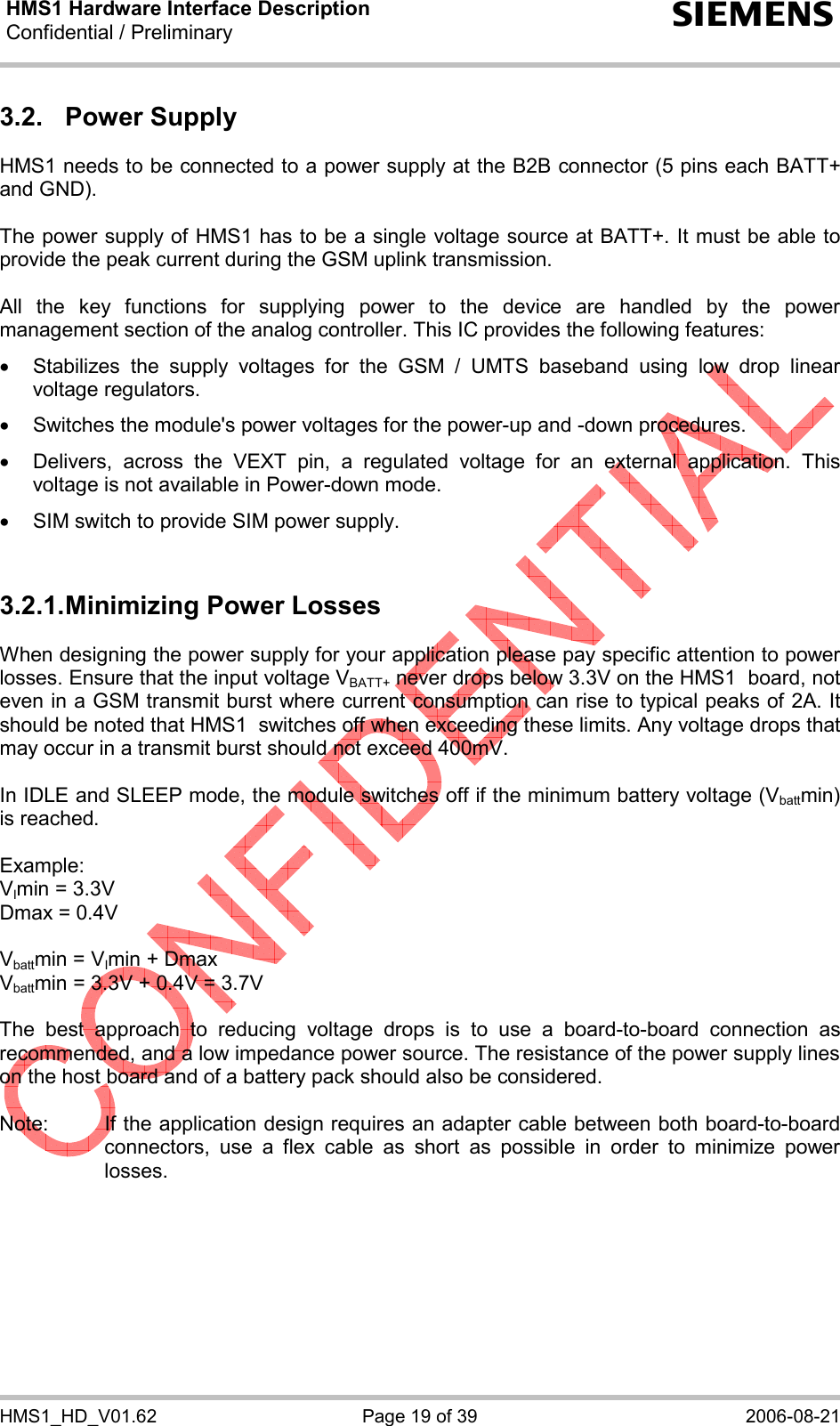
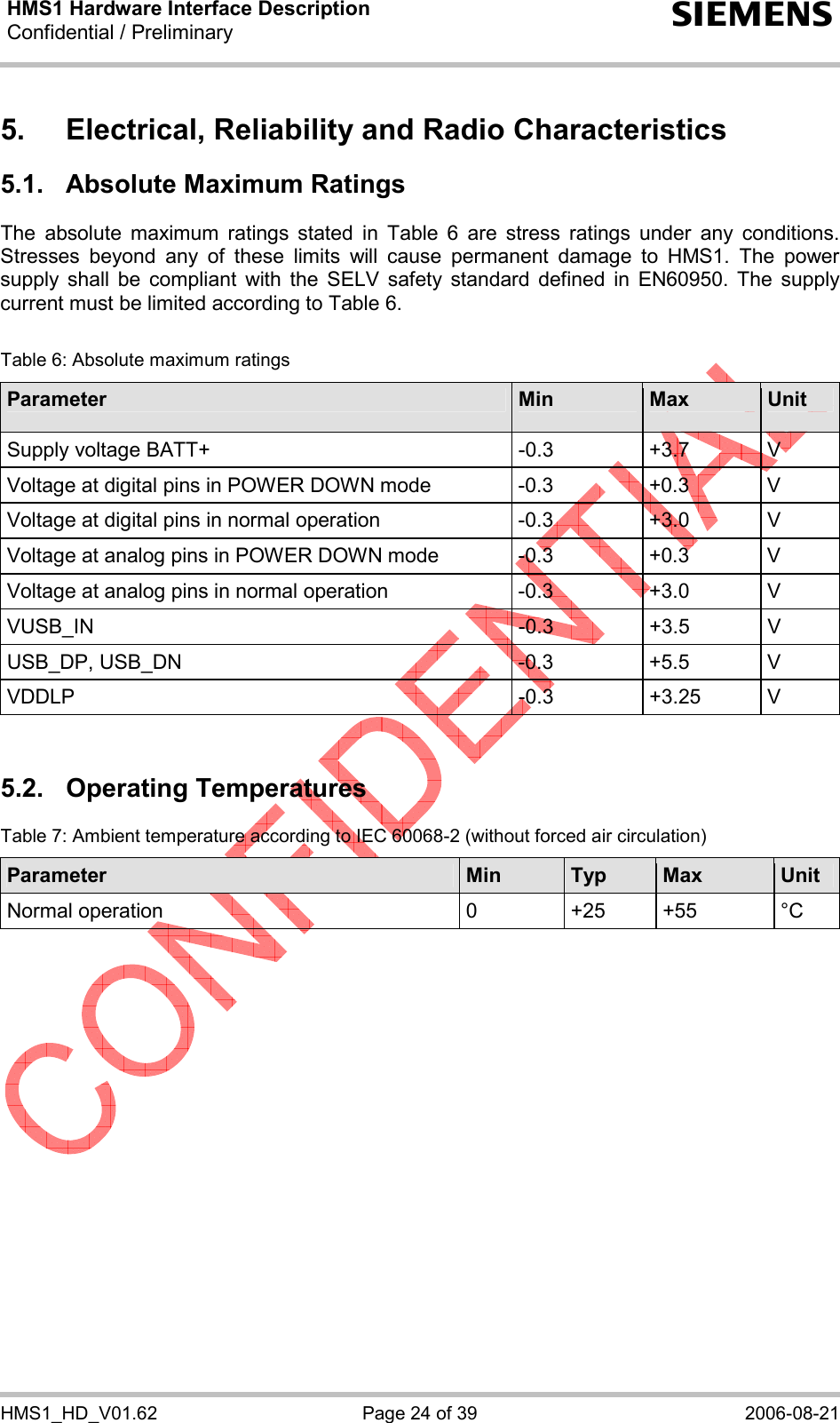
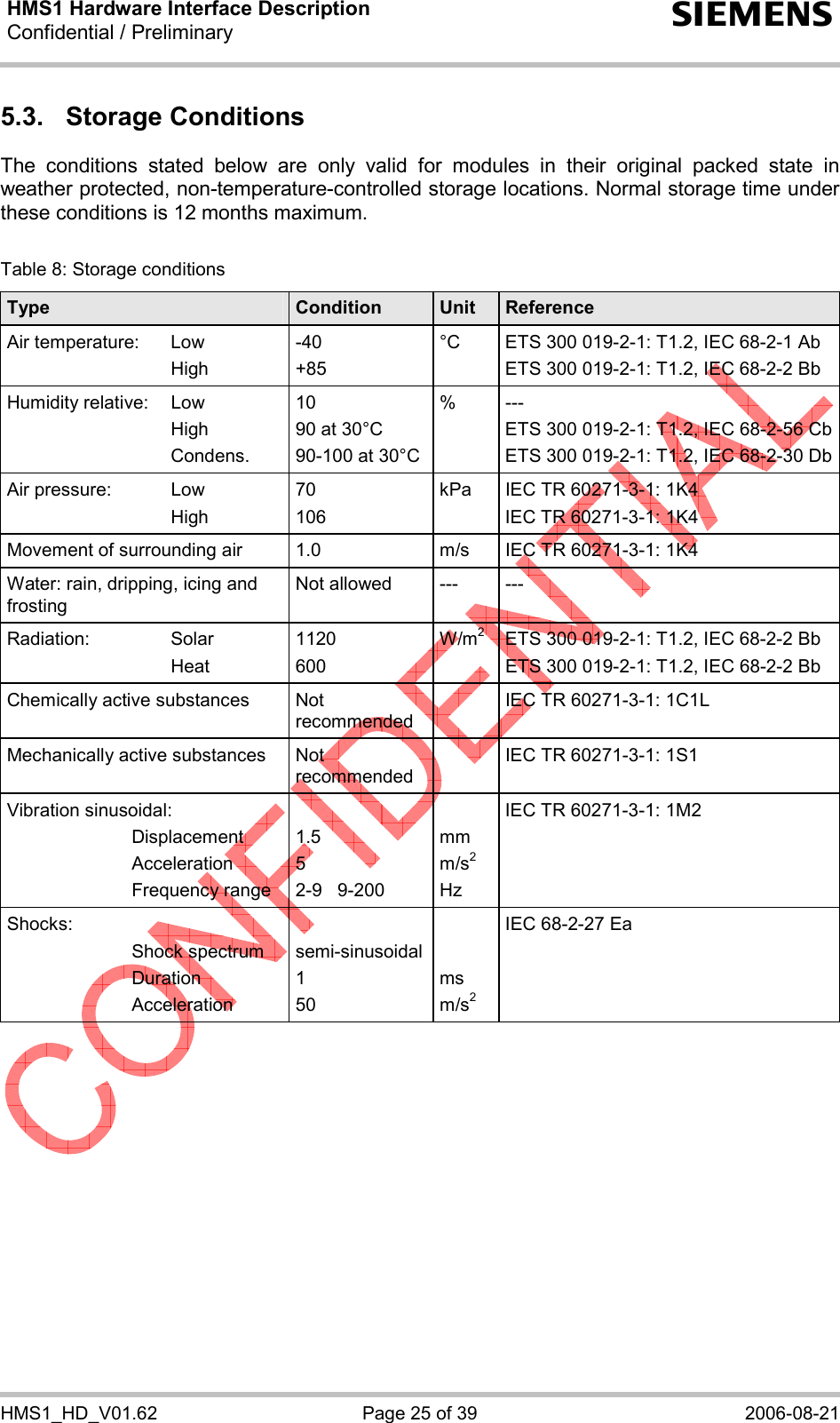
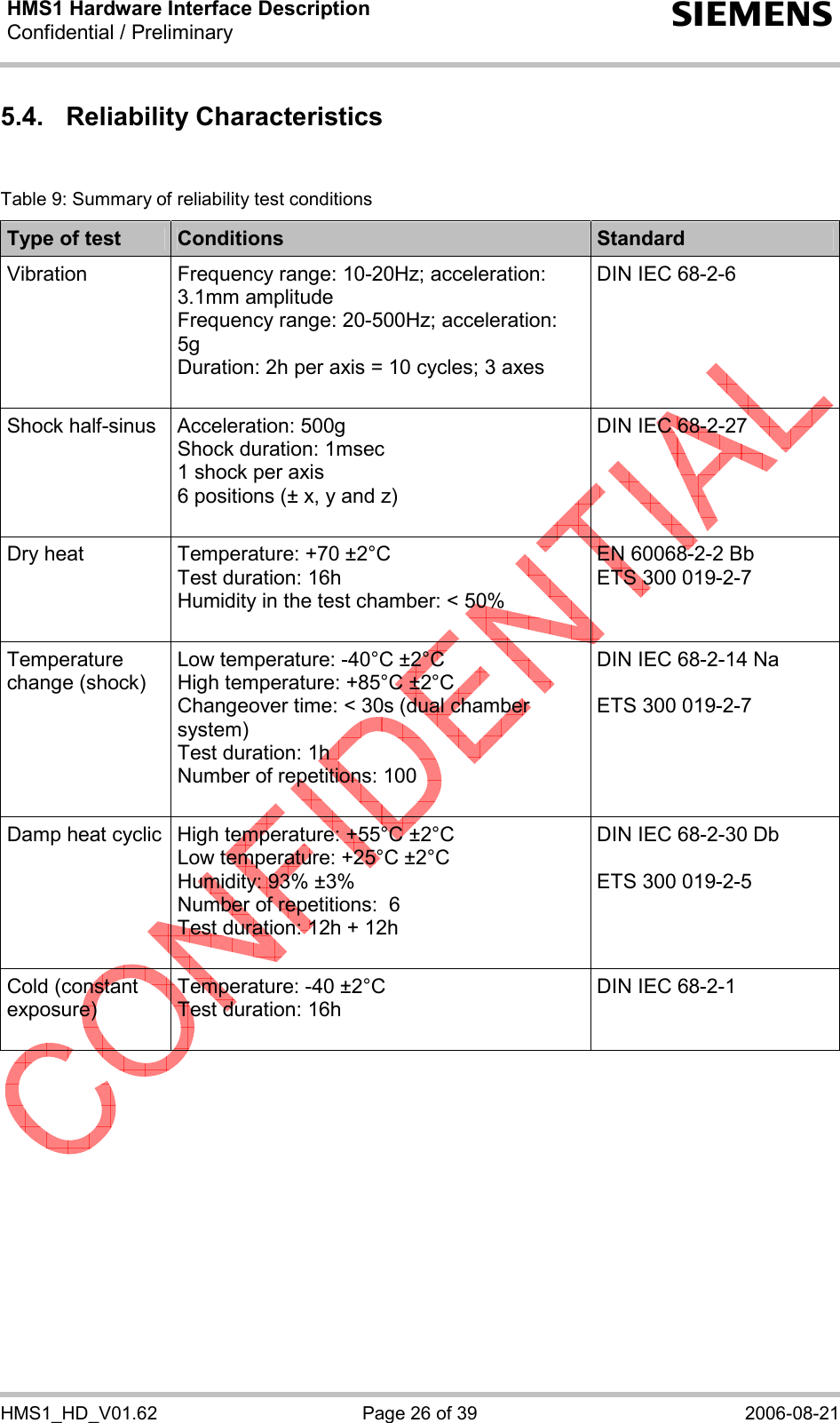
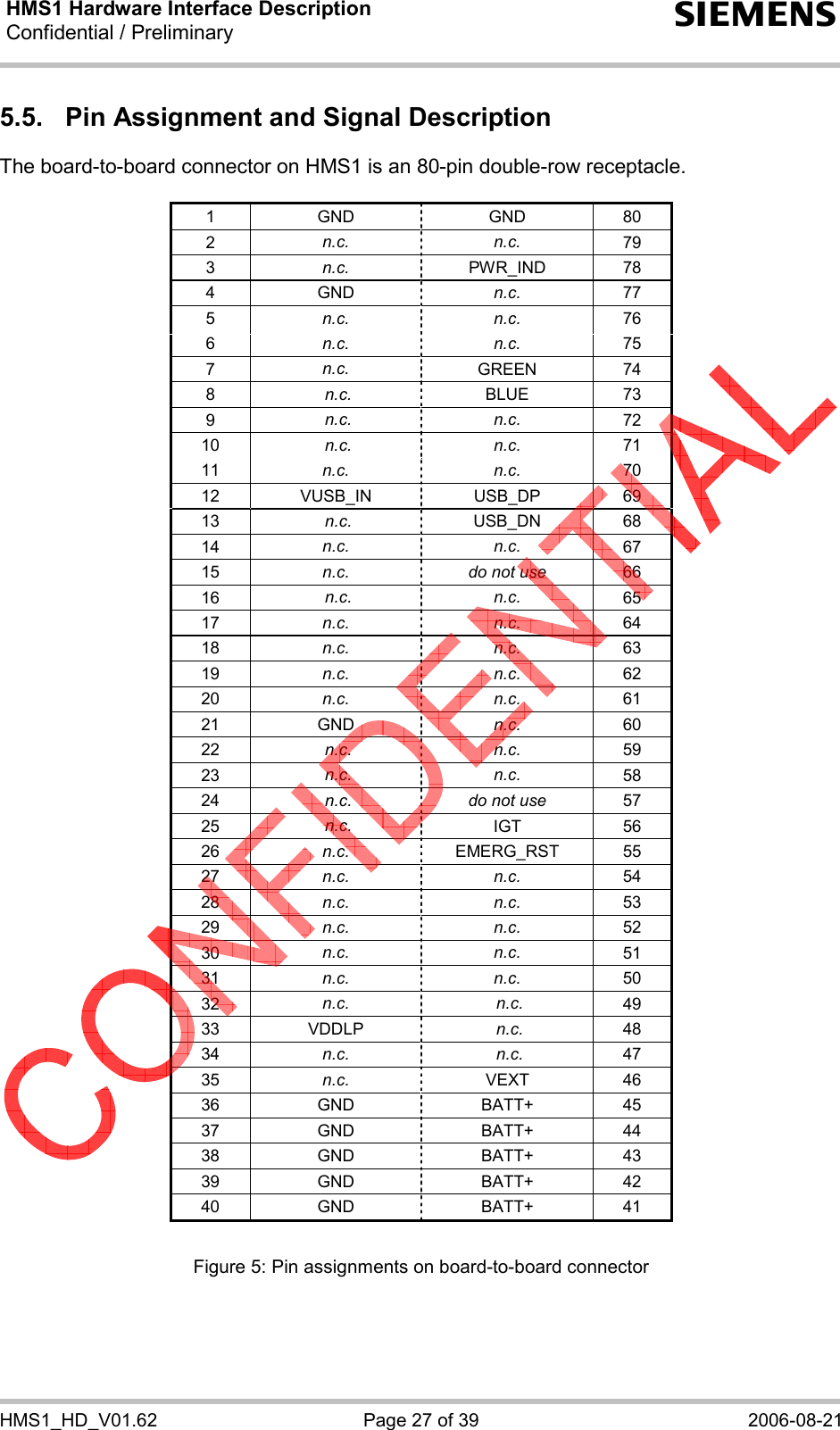
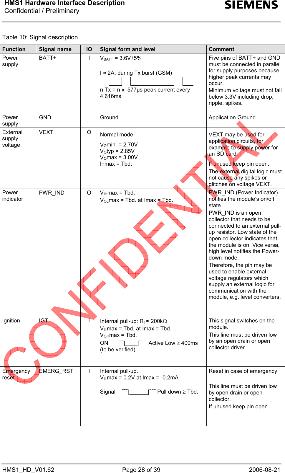
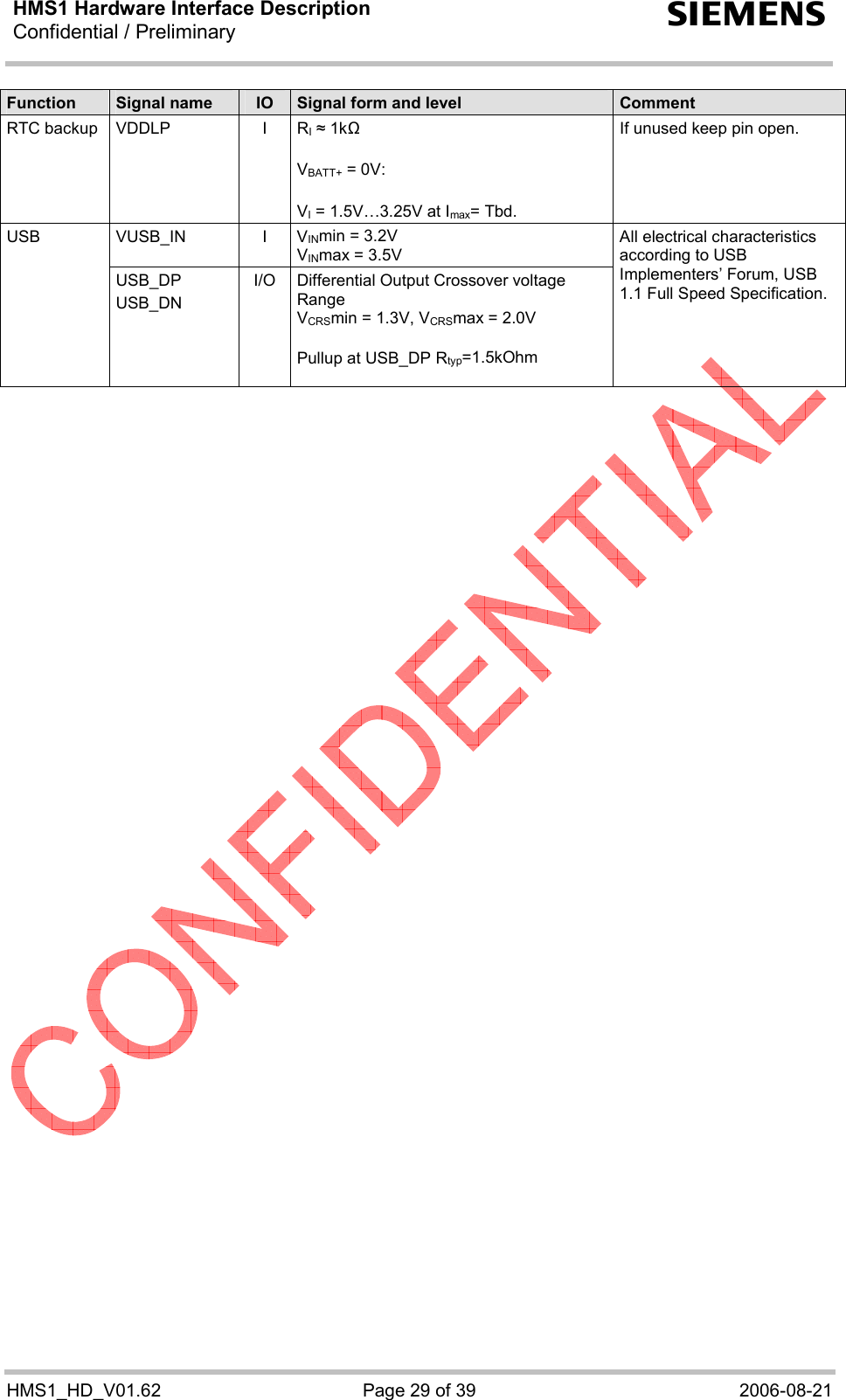
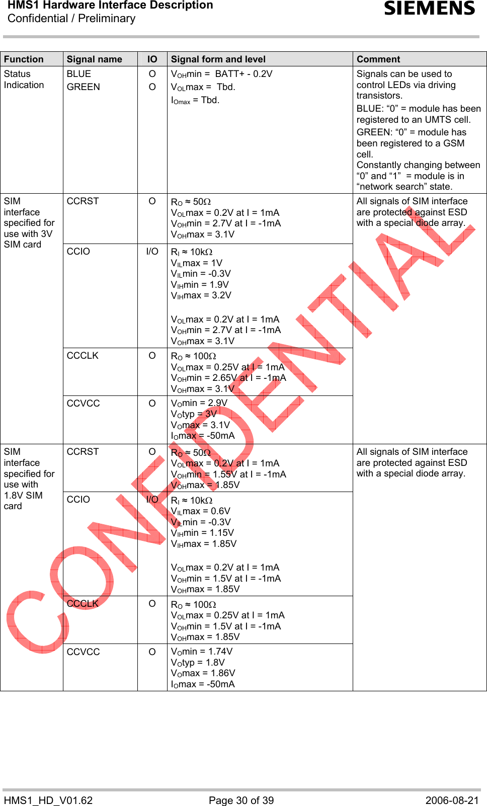
![HMS1 Hardware Interface Description Confidential / Preliminary s HMS1_HD_V01.62 Page 6 of 39 2006-08-21 1. Introduction This document describes the hardware of the Siemens HMS1 module that connects to a cellular device application and the air interface. It helps you quickly retrieve interface specifications, electrical and mechanical details and information on the requirements to be considered for integrating further components. The HMS1 module is a single band WCDMA, quad band GSM/GPRS data modem and features high downlink speeds using HSDPA. It can be connected to a standard PC via USB interface for high speed data communication, such as email, web browsing, data base retrieval, server access, as well as audio and video streaming. 1.1. Related Documents [1] HMS1 AT Command Set, Version 01.62 [2] DSB75 Support Box - Evaluation Kit for Siemens Cellular Engines 1.2. Terms and Abbreviations Abbreviation Description A/D Analog-to-Digital Converter AF Audio Frequency AFC Automatic Frequency Control AGC Automatic Gain Control AMR Adaptive Multi Rate ARP Antenna Reference Point ASIC Application Specific Integrated Circuit BB Baseband CPU Central Processing Unit CR Change Request CTR Common Technical Regulation DAI Digital Audio Interface /DCD Data Carrier Detect DFC Digital Frequency Centering DSB Development Support Board DSP Digital Signal Processor /DSR Data Set Ready /DTR Data Terminal Ready DTX Discontinuous transmission](https://usermanual.wiki/THALES-DIS-AlS-Deutschland/HMS1/User-Guide-716482-Page-6.png)