THALES DIS AlS Deutschland HMS1 Quadband GSM/GPRS/UMTS/HSDPA Module User Manual HMS1 Hardware Interface Description
Gemalto M2M GmbH Quadband GSM/GPRS/UMTS/HSDPA Module HMS1 Hardware Interface Description
Integration Manual

Hardware Interface Descri
p
tion
HMS1
Siemens Cellular Engine
Version: 01.62
DocID: HMS1_HD_V01.62

HMS1 Hardware Interface Description
Confidential / Preliminary s
HMS1_HD_V01.62 Page 2 of 39 2006-08-21
Document Name: HMS1 Hardware Interface Description
Version: 01.62
Date: August 21, 2006
DocId: HMS1_HD_V01.62
Status: Confidential / Preliminary
General note
Product is deemed accepted by Recipient and is provided without interface to Recipient´s products.
The Product constitutes pre-release version and code and may be changed substantially before
commercial release. The Product is provided on an “as is” basis only and may contain deficiencies or
inadequacies. The Product is provided without warranty of any kind, express or implied. To the
maximum extent permitted by applicable law, Siemens further disclaims all warranties, including
without limitation any implied warranties of merchantability, fitness for a particular purpose and
noninfringement of third-party rights. The entire risk arising out of the use or performance of the
Product and documentation remains with Recipient. This Product is not intended for use in life support
appliances, devices or systems where a malfunction of the product can reasonably be expected to
result in personal injury. Applications incorporating the described product must be designed to be in
accordance with the technical specifications provided in these guidelines. Failure to comply with any of
the required procedures can result in malfunctions or serious discrepancies in results. Furthermore, all
safety instructions regarding the use of mobile technical systems, including GSM products, which also
apply to cellular phones must be followed. Siemens AG customers using or selling this product for use
in any applications do so at their own risk and agree to fully indemnify Siemens for any damages
resulting from illegal use or resale. To the maximum extent permitted by applicable law, in no event
shall Siemens or its suppliers be liable for any consequential, incidental, direct, indirect, punitive or
other damages whatsoever (including, without limitation, damages for loss of business profits,
business interruption, loss of business information or data, or other pecuniary loss) arising out the use
of or inability to use the Product, even if Siemens has been advised of the possibility of such damages.
Subject to change without notice at any time.
Copyright
Transmittal, reproduction, dissemination and/or editing of this document as well as utilization of its
contents and communication thereof to others without express authorization are prohibited. Offenders
will be held liable for payment of damages. All rights created by patent grant or registration of a utility
model or design patent are reserved.
Copyright © Siemens AG 2006

HMS1 Hardware Interface Description
Confidential / Preliminary s
HMS1_HD_V01.62 Page 3 of 39 2006-08-21
Contents
0. Document History ...................................................................................................... 5
1. Introduction ................................................................................................................ 6
1.1. Related Documents............................................................................................. 6
1.2. Terms and Abbreviations .................................................................................... 6
1.3. Type Approval..................................................................................................... 9
1.4. Safety Precautions ............................................................................................ 11
2. Product Concept ...................................................................................................... 13
2.1. Key Features at a Glance.................................................................................. 13
2.2. HMS1 System Overview ................................................................................... 15
2.3. Circuit Concept.................................................................................................. 16
3. Application Interface................................................................................................ 17
3.1. Operating Modes............................................................................................... 18
3.2. Power Supply.................................................................................................... 19
3.2.1. Minimizing Power Losses .................................................................... 19
3.3. Power-Up / Power-Down Scenarios .................................................................. 20
3.3.1. Turn on HMS1 ..................................................................................... 20
3.3.2. Turn off HMS1 ..................................................................................... 20
3.4. Power Saving.................................................................................................... 21
3.5. RTC Backup...................................................................................................... 21
3.6. USIM Interface .................................................................................................. 21
3.7. USB Interface.................................................................................................... 21
3.8. Control Signals.................................................................................................. 22
3.8.1. PWR_IND Signal................................................................................. 22
3.8.2. Status Signals ..................................................................................... 22
4. Antenna Interface..................................................................................................... 23
4.1. Antenna Installation........................................................................................... 23
4.1.1. Test Antenna ....................................................................................... 23
5. Electrical, Reliability and Radio Characteristics.................................................... 24
5.1. Absolute Maximum Ratings............................................................................... 24
5.2. Operating Temperatures ................................................................................... 24
5.3. Storage Conditions............................................................................................ 25
5.4. Reliability Characteristics .................................................................................. 26
5.5. Pin Assignment and Signal Description............................................................. 27
5.6. Power Supply Ratings....................................................................................... 31
5.7. Air Interface....................................................................................................... 32
5.8. Electrostatic Discharge...................................................................................... 34
6. Mechanics................................................................................................................. 35
6.1. Mechanical Dimensions HMS1.......................................................................... 35
7. Board-to-Board Application Connector.................................................................. 37
8. Reference Approval ................................................................................................. 38
8.1. Reference Equipment for Type Approval........................................................... 38
8.2. Compliance with FCC Rules and Regulations ................................................... 39

HMS1 Hardware Interface Description
Confidential / Preliminary s
HMS1_HD_V01.62 Page 4 of 39 2006-08-21
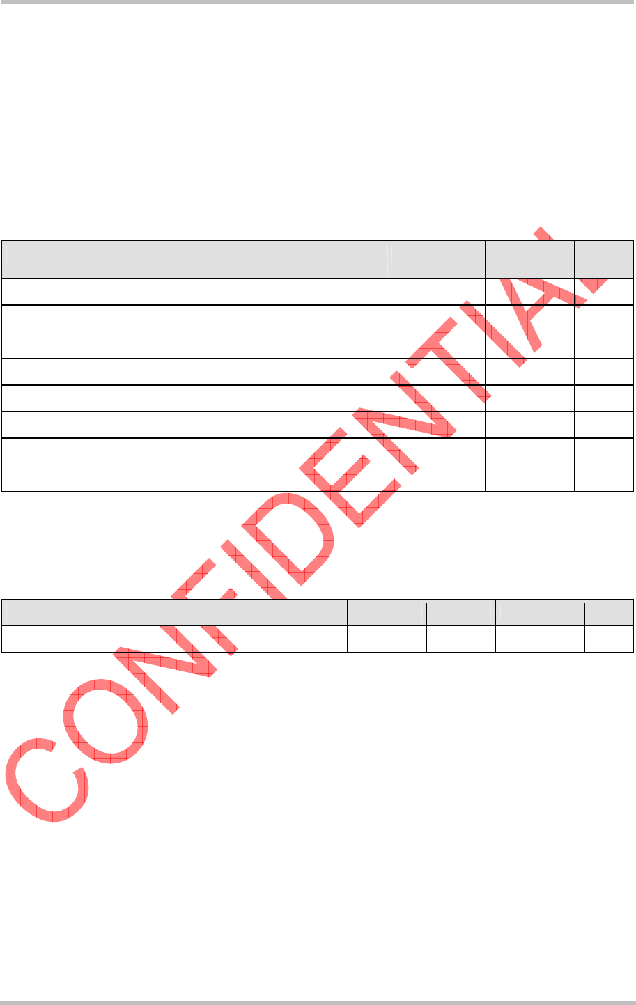
Tables
Table 1: Directives..................................................................................................................9
Table 2: Standards of North American type approval..............................................................9
Table 2: Standards of European type approval.......................................................................9
Table 3: Requirements of quality..........................................................................................10
Table 4: Overview of operating modes .................................................................................18
Table 5: Absolute maximum ratings......................................................................................24
Table 6: Ambient temperature according to IEC 60068-2 (without forced air circulation) ......24
Table 7: Storage conditions..................................................................................................25
Table 8: Summary of reliability test conditions......................................................................26
Table 9: Signal description ...................................................................................................28
Table 10: Power supply ratings ............................................................................................31
Table 11: Air Interface GSM .................................................................................................32
Table 12: Air Interface UMTS ...............................................................................................33
Table 13: Measured electrostatic values...............................................................................34
Table 14: Electrical and mechanical characteristics of the 80 pin board-to-board connector.37
Figures
Figure 1: HSM system overview ...........................................................................................15
Figure 2: HMS1 schematic overview ....................................................................................16
Figure 3: Power supply limits during transmit burst...............................................................20
Figure 5: Internal antenna for HMS.......................................................................................23
Figure 6: Pin assignments on board-to-board connector ......................................................27
Figure 7: HMS1 Top View (prelim.).......................................................................................35
Figure 8: HMS1 Dimensions (prelim.)...................................................................................36
Figure 9: Mechanical dimensions of 80 pin board-to-board connector ..................................37
Figure 10: Reference equipment for Type Approval .............................................................38


HMS1 Hardware Interface Description
Confidential / Preliminary s
HMS1_HD_V01.62 Page 6 of 39 2006-08-21
1. Introduction
This document describes the hardware of the Siemens HMS1 module that connects to a
cellular device application and the air interface. It helps you quickly retrieve interface
specifications, electrical and mechanical details and information on the requirements to be
considered for integrating further components.
The HMS1 module is a single band WCDMA, quad band GSM/GPRS data modem and
features high downlink speeds using HSDPA. It can be connected to a standard PC via USB
interface for high speed data communication, such as email, web browsing, data base
retrieval, server access, as well as audio and video streaming.
1.1. Related Documents
[1] HMS1 AT Command Set, Version 01.62
[2] DSB75 Support Box - Evaluation Kit for Siemens Cellular Engines
1.2. Terms and Abbreviations
Abbreviation Description
A/D Analog-to-Digital Converter
AF Audio Frequency
AFC Automatic Frequency Control
AGC Automatic Gain Control
AMR Adaptive Multi Rate
ARP Antenna Reference Point
ASIC Application Specific Integrated Circuit
BB Baseband
CPU Central Processing Unit
CR Change Request
CTR Common Technical Regulation
DAI Digital Audio Interface
/DCD Data Carrier Detect
DFC Digital Frequency Centering
DSB Development Support Board
DSP Digital Signal Processor
/DSR Data Set Ready
/DTR Data Terminal Ready
DTX Discontinuous transmission

HMS1 Hardware Interface Description
Confidential / Preliminary s
HMS1_HD_V01.62 Page 7 of 39 2006-08-21
EFR Enhanced Full Rate
EMC Electro Magnetic Compatibility
EGSM Enhanced GSM
ESD Electrostatic Discharge
ESR Equivalent Serial Resistance
ETS European Telecommunication Standard
FE Front-End
FFC Flat Flexible Cable
FR Full Rate
GMSK Gaussian Minimum Shift Keying
GSC (Type of antenna connector)
GSM Global Standard for Mobile Communications
HR Half Rate
HSDPA High Speed Downlink Packet Access
HW Hardware
IC Integrated Circuit
IF Intermediate Frequency
IMEI International Mobile Equipment Identity
I/O Input/Output
ISO International Standards Organization
ITU International Telecommunications Union
LDO Low Drop Out
LFBGA Low-Profile Fine-Pitch Ball Grid Array
Li-Ion Lithium-Ion
LNA Low Noise Amplifier
LO Local Oscillator
Mbps Mbit per second
MMI Man Machine Interface
MTBF Mean Time Between Failures
NTC Negative Temperature Coefficient
OC Offset Compensation
OTP One Time Programmable
PA(C) Power Amplifier (Control)
PCB Printed Circuit Board
PCM Pulse Code Modulation
PD Power Down
PGC Programmable Gain-Controlled Amplifier

HMS1 Hardware Interface Description
Confidential / Preliminary s
HMS1_HD_V01.62 Page 8 of 39 2006-08-21
PLL Phase Locked Loop
PSU Power Supply Unit
RAM Random Access Memory
RF Radio Frequency
/RING Ring Indication
ROM Read-Only Memory
RTC Real Time Clock
/RXD Receive direction
Rx Receive direction
SAW Surface Acoustical Wave Filter
SELV Safety Extra Low Voltage
SIM Subscriber Identification Module
SMS Short Message Service
SRAM Static Random Access Memory
SW Software
TBR Technical Based Regulation
TBD To Be Defined
TBI To Be Inserted
TDD Time Division Duplex
TDMA Time Division Multiple Access
/TXD Transmit direction
Tx Transmit direction
UART Universal Asynchronous Receiver Transmitter
VCO Voltage Controlled Oscillator
VCXO Voltage Controlled Quartz Oscillator
VSWR Voltage Standing Wave Ratio
HMS1 Hardware Interface Description
Confidential / Preliminary s
HMS1_HD_V01.62 Page 9 of 39 2006-08-21
1.3. Type Approval
HMS1 has been approved to comply with the directives and standards listed below.
Table 1: Directives
99/05/EC Directive of the European Parliament and of the council of 9
March 1999 on radio equipment and telecommunications terminal
equipment and the mutual recognition of their conformity (in short
referred to as R&TTE Directive 1999/5/EC).
The product is labeled with the CE conformity mark
89/336/EC Directive on electromagnetic compatibility
73/23/EC Directive on electrical equipment designed for use within certain
voltage limits (Low Voltage Directive)
2002/95/EC Directive of the European Parliament and of the
Council of 27 January 2003 on the restriction of the
use of certain hazardous substances in electrical
and electronic equipment (RoHS)
Table 2: Standards of North American type approval
CFR Title 47 Code of Federal Regulations, Part 22 and Part 24
(Telecommunications, PCS); US Equipment Authorization FCC
NAPRD.03 V3.5.1 Overview of PCS Type certification review board Mobile
Equipment Type Certification and IMEI control
PCS Type Certification Review board (PTCRB)
RSS133 (Issue2) Canadian Standard
Table 3: Standards of European type approval
3GPP TS 51.010-1 Digital cellular telecommunications system (Phase 2); Mobile
Station (MS) conformance specification
ETSI EN 301 511
V9.0.2
Candidate Harmonized European Standard (Telecommunications
series) Global System for Mobile communications (GSM);
Harmonized standard for mobile stations in the GSM 900 and
DCS 1800 bands covering essential requirements under article
3.2 of the R&TTE directive (1999/5/EC) (GSM 13.11 version 7.0.1
Release 1998)
GCF-CC V3.xx.0 Global Certification Forum - Certification Criteria
ETSI EN 301 489-1
V1.4.1
Candidate Harmonized European Standard (Telecommunications
series) Electro Magnetic Compatibility and Radio spectrum Matters
(ERM); Electro Magnetic Compatibility (EMC) standard for radio
equipment and services; Part 1: Common Technical Requirements

HMS1 Hardware Interface Description
Confidential / Preliminary s
HMS1_HD_V01.62 Page 10 of 39 2006-08-21
ETSI EN 301 489-7
V1.2.1 (2000-09)
Candidate Harmonized European Standard (Telecommunications
series) Electro Magnetic Compatibility and Radio spectrum
Matters (ERM); Electro Magnetic Compatibility (EMC) standard for
radio equipment and services; Part 7: Specific conditions for
mobile and portable radio and ancillary equipment of digital
cellular radio telecommunications systems (GSM and DCS)
IEC/EN 60950-1
(2001)
Safety of information technology equipment (2000)
Table 4: Requirements of quality
IEC 60068 Environmental testing
DIN EN 60529 IP codes
SAR requirements specific to portable mobiles
Mobile phones, PDAs or other portable transmitters and receivers incorporating a GSM
module must be in accordance with the guidelines for human exposure to radio frequency
energy. This requires the Specific Absorption Rate (SAR) of portable HMS1 based
applications to be evaluated and approved for compliance with national and/or international
regulations.
Since the SAR value varies significantly with the individual product design manufacturers are
advised to submit their product for approval if designed for portable use. For European and
US markets the relevant directives are mentioned below. It is the responsibility of the
manufacturer of the final product to verify whether or not further standards, recommendations
or directives are in force outside these areas.
Products intended for sale on US markets
ES 59005/ANSI C95.1 Considerations for evaluation of human exposure to
Electromagnetic Fields (EMFs) from Mobile Telecommunication
Equipment (MTE) in the frequency range 30MHz - 6GHz
Products intended for sale on European markets
EN 50360 Product standard to demonstrate the compliance of mobile phones
with the basic restrictions related to human exposure to
electromagnetic fields (300MHz - 3GHz)
HMS1 Hardware Interface Description
Confidential / Preliminary s
HMS1_HD_V01.62 Page 11 of 39 2006-08-21
1.4. Safety Precautions
The following safety precautions must be observed during all phases of the operation, usage,
service or repair of any cellular terminal or mobile incorporating HMS1. Manufacturers of the
cellular terminal are advised to convey the following safety information to users and
operating personnel and to incorporate these guidelines into all manuals supplied with the
product. Failure to comply with these precautions violates safety standards of design,
manufacture and intended use of the product. Siemens AG assumes no liability for
customer’s failure to comply with these precautions.
When in a hospital or other health care facility, observe the restrictions on the
use of mobiles. Switch the cellular terminal or mobile off, if instructed to do so
by the guidelines posted in sensitive areas. Medical equipment may be
sensitive to RF energy.
The operation of cardiac pacemakers, other implanted medical equipment
and hearing aids can be affected by interference from cellular terminals or
mobiles placed close to the device. If in doubt about potential danger, contact
the physician or the manufacturer of the device to verify that the equipment is
properly shielded. Pacemaker patients are advised to keep their hand-held
mobile away from the pacemaker, while it is on.
Switch off the cellular terminal or mobile before boarding an aircraft. Make
sure it cannot be switched on inadvertently. The operation of wireless
appliances in an aircraft is forbidden to prevent interference with
communications systems. Failure to observe these instructions may lead to
the suspension or denial of cellular services to the offender, legal action, or
both.
Do not operate the cellular terminal or mobile in the presence of flammable
gases or fumes. Switch off the cellular terminal when you are near petrol
stations, fuel depots, chemical plants or where blasting operations are in
progress. Operation of any electrical equipment in potentially explosive
atmospheres can constitute a safety hazard.
Your cellular terminal or mobile receives and transmits radio frequency
energy while switched on. Remember that interference can occur if it is used
close to TV sets, radios, computers or inadequately shielded equipment.
Follow any special regulations and always switch off the cellular terminal or
mobile wherever forbidden, or when you suspect that it may cause
interference or danger.
Road safety comes first! Do not use a hand-held cellular terminal or mobile
when driving a vehicle, unless it is securely mounted in a holder for
speakerphone operation. Before making a call with a hand-held terminal or
mobile, park the vehicle.
Speakerphones must be installed by qualified personnel. Faulty installation or
operation can constitute a safety hazard.

HMS1 Hardware Interface Description
Confidential / Preliminary s
HMS1_HD_V01.62 Page 12 of 39 2006-08-21
SOS
IMPORTANT!
Cellular terminals or mobiles operate using radio signals and cellular
networks. Because of this, connection cannot be guaranteed at all times
under all conditions. Therefore, you should never rely solely upon any
wireless device for essential communications, for example emergency calls.
Remember, in order to make or receive calls, the cellular terminal or mobile
must be switched on and in a service area with adequate cellular signal
strength.
Some networks do not allow for emergency calls if certain network services or
phone features are in use (e.g. lock functions, fixed dialing etc.). You may
need to deactivate those features before you can make an emergency call.
Some networks require that a valid SIM card be properly inserted in the
cellular terminal or mobile.

HMS1 Hardware Interface Description
Confidential / Preliminary s
HMS1_HD_V01.62 Page 13 of 39 2006-08-21
2. Product Concept
2.1. Key Features at a Glance
Feature Implementation
General
Frequency bands Quad band: GSM 850/900/1800/1900MHz
Single band: WCDMA 2100
GSM class Small MS
Output power
(according to
Release 99, V5)
Class 4 (+33dBm ±2dB) for EGSM850
Class 4 (+33dBm ±2dB) for EGSM900
Class 1 (+30dBm ±2dB) for GSM1800
Class 1 (+30dBm ±2dB) for GSM1900
Class E2 (+27dBm ± 3dB) for GSM 850 8-PSK
Class E2 (+27dBm ± 3dB) for GSM 900 8-PSK
Class E2 (+26dBm +3 /-4dB) for GSM 1800 8-PSK
Class E2 (+26dBm +3 /-4dB) for GSM 1900 8-PSK
Class 3 (+24dBm +1/-3dB) for UMTS 2100, WCDMA FDD BdI
The values stated above are maximum limits. According to
Release 99, Version 5, the maximum output power in a multislot
configuration may be lower. The nominal reduction of maximum
output power varies with the number of uplink timeslots used and
amounts to 3.0dB for 2Tx.
Power supply 3.6V, supplied by limited power source
Ambient operating
temperature according
to IEC 60068-2
Normal operation
0°C to 55°C
Physical Dimensions: 70mm x 49.7mm x 5mm
Weight: approx. 17g
RoHS All hardware components fully compliant with EU RoHS Directive
GSM / GPRS / EGPRS / UMTS features
Data transfer UMTS
• FDD Mode
• HSDPA Mode Cat. 11.12
•
GPRS
• Multislot Class 10
• Full PBCCH support
• Mobile Station Class B
• Coding Scheme 1 – 4

HMS1 Hardware Interface Description
Confidential / Preliminary s
HMS1_HD_V01.62 Page 14 of 39 2006-08-21
Feature Implementation
EGPRS
• Multislot Class 10
• Mobile Station Class B
• Modulation and Coding Scheme MCS 1 – 9
CSD
• V.110, RLP, non-transparent
• GSM: 2.4, 4.8, 9.6, 14.4kbps
• UMTS: 57.6kbps
SMS • Point-to-point MT and MO
• Cell broadcast
• Text and PDU mode
Fax Group 3; Class 1, Class 2
Software
AT commands AT-Hayes GSM 07.05 and 07.07, Qualcomm
AT command Set
Firmware update Generic update from host application over USB.
Interfaces
USB Supports a USB 1.1 Full Speed (12Mbit/s) device interface.
SIM SIM card reader on board
Antenna External antenna can be connected via antenna pads. For test
purposes a 50Ohm antenna can be connected via coaxial switch
(Hirose MS-156NB).
Module interface 80 pin board-to-board connector
Power on/off, Reset
Power on/off • Switch-on by hardware pin IGT
• Switch-off by AT command
Reset • Orderly shutdown and reset by AT command
• Emergency reset by hardware pins EMERG_RST
Evaluation kit
DSB DSB Evaluation Board designed to test and type approve
Siemens cellular engines and provide a sample configuration for
application engineering.
HMS1 Hardware Interface Description
Confidential / Preliminary s
HMS1_HD_V01.62 Page 15 of 39 2006-08-21
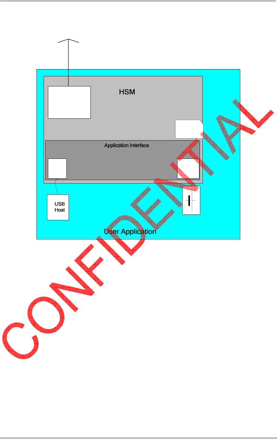
2.2. HMS1 System Overview
Antenna
Interface
USB Power
Supply
Sim card
holder
Figure 1: HSM system overview
HMS1 Hardware Interface Description
Confidential / Preliminary s
HMS1_HD_V01.62 Page 16 of 39 2006-08-21
2.3. Circuit Concept
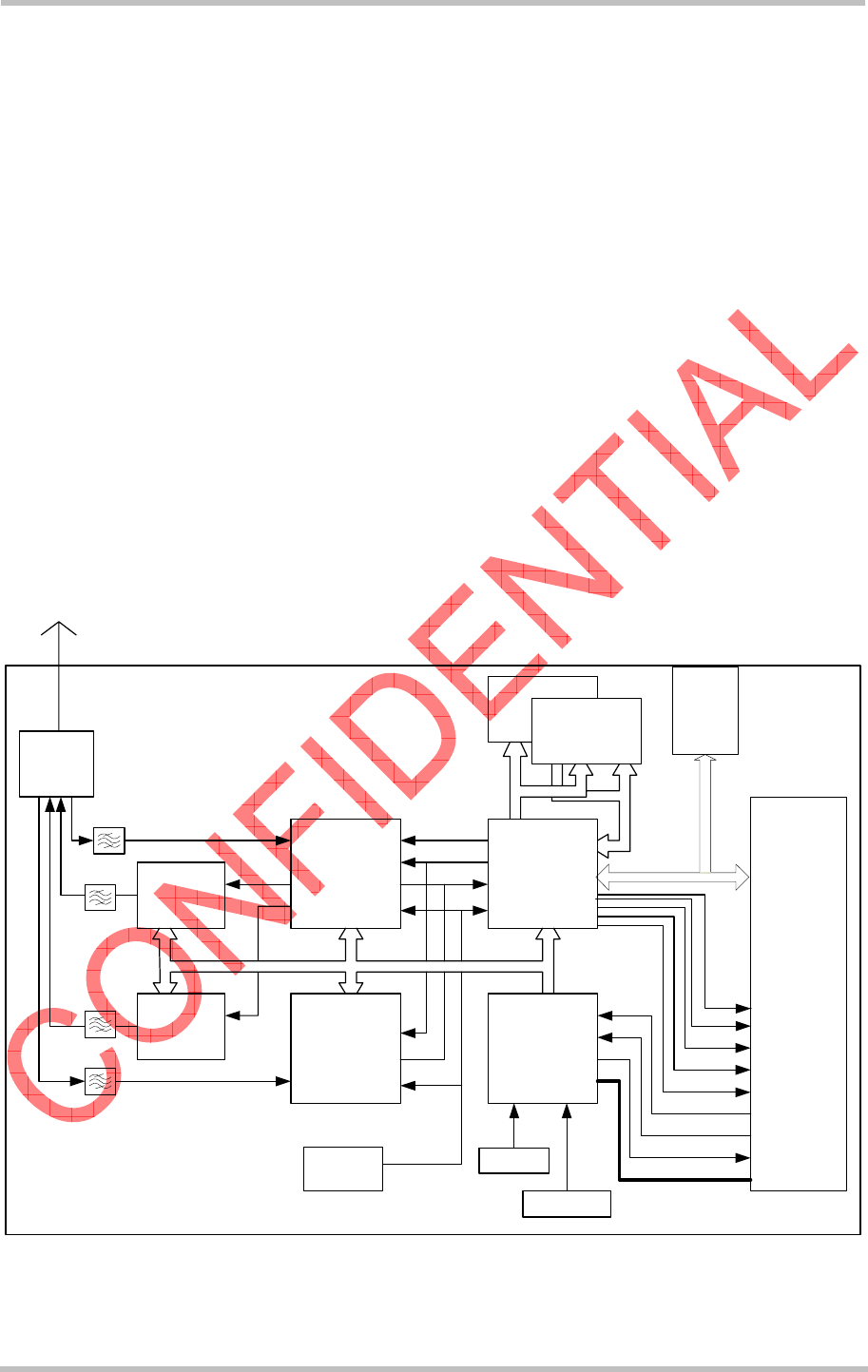
Figure 2 shows a block diagram of the HMS module and illustrates the major functional
components:
Base band block:
• WCDMA/GSM Baseband Controller
• Power supply unit
• Flash/SDRAM memory
• External Interface, 80 pin board-to-board connector
RF section:
• RF WCDMA Receiver
• RF WCDMA Transmitter
• RF Power Amplifiers
• EPCOS receive SAWs (according to variant – see below)
• Antenna Connector
B2B
Connector
Processor
Power
Management
Transceiver
Receiver
GSM
PA
WCDMA
PA
Frontend
48MHz
32.786kHz
TCTCXO
19.2MHz
NAND
Flash
SDRAM
USB
PWR_IND
EMERG_RST
CONTROL
IGT
VEXT
BATT+
VDDLP
Green
Blue
SIM
Card
Holder
Figure 2: HMS1 schematic overview

HMS1 Hardware Interface Description
Confidential / Preliminary s
HMS1_HD_V01.62 Page 17 of 39 2006-08-21
3. Application Interface
HMS1 is equipped with an 80 pin board-to-board connector that connects to the external
application. The host interface incorporates several sub-interfaces described in the following
chapters:
• Operation Modes - see Section 3.1
• Power supply - see Section 3.2
• SIM interface - see Section 3.6
• Serial interface USB - see Section 3.7.
• Status and control lines: IGT, EMERG_RST, PWR_IND, STATUS1/2 – see Table 10

HMS1 Hardware Interface Description
Confidential / Preliminary s
HMS1_HD_V01.62 Page 18 of 39 2006-08-21
3.1. Operating Modes
The table below briefly summarizes the various operating modes referred to in the following
chapters.
Table 5: Overview of operating modes
GSM / GPRS
SLEEP
Tbd.
GSM IDLE Software is active. Once registered to the GSM
network, paging with BTS is carried out. The
module is ready to send and receive.
GSM DATA Connection between two subscribers is in
progress. Power consumption depends on network
coverage individual settings.
GPRS IDLE
EGPRS IDLE
Module is ready for GPRS/EGPRS data transfer,
but no data is currently sent or received. Power
consumption depends on network settings and
GPRS/EGPRS configuration (e.g. multislot
settings).
GPRS DATA
EGPRS DATA
GPRS/EGPRS data transfer in progress. Power
consumption depends on network settings (e.g.
power control level), uplink / downlink data rates,
GPRS/EGPRS configuration (e.g. used multislot
settings) and reduction of maximum output power.
UMTS IDLE Software is active. Once registered to the UMTS
network, paging with BTS is carried out. The
module is ready to send and receive.
UMTS DATA UMTS Data Transfer in progress.
Normal operation
HSDPA HSDPA High Speed Data connection in Downlink
Direction.
POWER DOWN Normal shutdown after sending the AT command.
Operating voltage (connected to BATT+) remains applied.

HMS1 Hardware Interface Description
Confidential / Preliminary s
HMS1_HD_V01.62 Page 19 of 39 2006-08-21
3.2. Power Supply
HMS1 needs to be connected to a power supply at the B2B connector (5 pins each BATT+
and GND).
The power supply of HMS1 has to be a single voltage source at BATT+. It must be able to
provide the peak current during the GSM uplink transmission.
All the key functions for supplying power to the device are handled by the power
management section of the analog controller. This IC provides the following features:
• Stabilizes the supply voltages for the GSM / UMTS baseband using low drop linear
voltage regulators.
• Switches the module's power voltages for the power-up and -down procedures.
• Delivers, across the VEXT pin, a regulated voltage for an external application. This
voltage is not available in Power-down mode.
• SIM switch to provide SIM power supply.
3.2.1. Minimizing Power Losses
When designing the power supply for your application please pay specific attention to power
losses. Ensure that the input voltage VBATT+ never drops below 3.3V on the HMS1 board, not
even in a GSM transmit burst where current consumption can rise to typical peaks of 2A. It
should be noted that HMS1 switches off when exceeding these limits. Any voltage drops that
may occur in a transmit burst should not exceed 400mV.
In IDLE and SLEEP mode, the module switches off if the minimum battery voltage (Vbattmin)
is reached.
Example:
VImin = 3.3V
Dmax = 0.4V
Vbattmin = VImin + Dmax
Vbattmin = 3.3V + 0.4V = 3.7V
The best approach to reducing voltage drops is to use a board-to-board connection as
recommended, and a low impedance power source. The resistance of the power supply lines
on the host board and of a battery pack should also be considered.
Note: If the application design requires an adapter cable between both board-to-board
connectors, use a flex cable as short as possible in order to minimize power
losses.

HMS1 Hardware Interface Description
Confidential / Preliminary s
HMS1_HD_V01.62 Page 20 of 39 2006-08-21
Example: If the length of the flex cable reaches the maximum length of 100mm, this
connection may cause, for example, a resistance of 30mΩ in the BATT+ line and
30mΩ in the GND line. As a result, a 2A transmit burst would add up to a total
voltage drop of 120mV. Plus, if a battery pack is involved, further losses may
occur due to the resistance across the battery lines and the internal resistance of
the battery including its protection circuit.
Figure 3: Power supply limits during transmit burst
3.3. Power-Up / Power-Down Scenarios
In general, be sure not to turn on HMS1 while it is beyond the safety limits of voltage and
temperature. HMS1 would immediately switch off after having started and detected these
inappropriate conditions. In extreme cases this can cause permanent damage to the module.
3.3.1. Turn on HMS1
When the HMS1 module is in Power-down mode, it can be started to Normal mode or
Airplane mode by driving the IGT (ignition) line to ground. This must be accomplished with an
open drain/collector driver to avoid current flowing into this pin.
3.3.1.1. Reset or Turn off HMS1 in Case of Emergency
Caution: Use the EMERG_RST pin only when, due to serious problems, the software is not
responding for more than 5 seconds. Pulling the EMERG_RST pin causes the loss of all
information stored in the volatile memory. Therefore, this procedure is intended only for use
in case of emergency, e.g. if HMS1 does not respond, if reset or shutdown via AT command
fails.
The EMERG_RST signal is available on the application interface.
3.3.2. Turn off HMS1
HMS1 can be turned off by Normal shutdown: Software controlled by AT command.
Be sure not to disconnect the supply voltage VBATT+. Otherwise you run the risk of losing
data.
Transmit
burst 2A
Transmit
burst 2A
Rippl
e
Drop
min. 3.3V
BATT+

HMS1 Hardware Interface Description
Confidential / Preliminary s
HMS1_HD_V01.62 Page 21 of 39 2006-08-21
3.4. Power Saving
Intended for power saving, SLEEP mode reduces the functionality of the HMS1 to a
minimum and thus minimizes the current consumption.
The different sleep modes will be specified later.
3.5. RTC Backup
The internal Real Time Clock of HMS1 is supplied from a separate voltage regulator in the
analog controller which is also active when HMS1 is in POWER DOWN status.
In addition, you can use the VDDLP pin on the board-to-board connector to backup the RTC
from an external capacitor or a battery (rechargeable or non-chargeable). The capacitor or
battery is charged by the power management controller of HMS1. If the voltage supply at
BATT+ is disconnected, the RTC can be powered by the capacitor or battery. The size of the
capacitor determines the duration of buffering when no voltage is applied to HMS1, i.e. the
larger the capacitor the longer HMS1 will save the date and time.
3.6. USIM Interface
The base band processor has an integrated SIM interface compatible with the 34.121 USIM
Testing IC Card standard. This is wired to an integrated SIM card holder. The USIM interface
supports 3V and 1.8V USIM cards.
Note: No guarantee can be given, nor any liability accepted, if loss of data is encountered
after removing the SIM card during operation.
Also, no guarantee can be given for properly initializing any SIM card that the user
inserts after having removed a SIM card during operation.
3.7. USB Interface
HMS1 supports a USB 1.1 Full Speed (12Mbit/s) device interface. The USB interface is the
recommended communication interface for high speed data transmission.
To properly connect the module’s USB interface to the host a USB 2.0 full speed compatible
connector is required. The HMS1 distribution contains the suitable USB driver to operate
HMS1 over USB. It is recommended to use this drive.
The USB host is responsible for supplying, across the VUSB_IN line, power to the module’s
USB interface, but not to other HMS1 interfaces. This is because HMS1 is designed as a
self-powered device compliant with the “Universal Serial Bus Specification Revision 1.1” (The
specification is ready for download on http://www.usb.org/developers/docs/).

HMS1 Hardware Interface Description
Confidential / Preliminary s
HMS1_HD_V01.62 Page 22 of 39 2006-08-21
3.8. Control Signals
Several control lines are signaling the states of the HMS1 module or control the module.
These states are power down, stand by, paging, GSM voice call, GSM data call, UMTS voice
call, UMTS data call or HSDPA connection.
3.8.1. PWR_IND Signal
PWR_IND notifies the on/off state of the module. High state of PWR_IND indicates that the
module is switched off. The state of PWR_IND immediately changes to low when IGT is
pulled low. For state detection an external pull-up resistor is required.
3.8.2. Status Signals
Two status signals (GREEN, BLUE) are provided for signaling the module’s connectivity
status:
• When searching for a network the signal 1 (GREEN) alternates at 2Hz
• When registered with a GSM network signal 1 is active
• When registered with a WCDMA network signal 2 (BLUE) goes active, signal 1 inactive

HMS1 Hardware Interface Description
Confidential / Preliminary s
HMS1_HD_V01.62 Page 23 of 39 2006-08-21
4. Antenna Interface
The RF interface has an impedance of 50Ω. HMS1 is capable of sustaining a total mismatch
at the antenna connector or pad without any damage, even when transmitting at maximum
RF power.
The external antenna must be matched properly to achieve best performance regarding
radiated power, DC-power consumption, modulation accuracy and harmonic suppression.
Antenna matching networks are not included on the HMS1 PCB and should be placed in the
host application.
The connection of the antenna or other equipment must be decoupled from DC voltage. This
is necessary because the antenna connector is DC coupled to ground via an inductor for
ESD protection.
4.1. Antenna Installation
To suit application requirements the HMS1 module adapts an internal antenna from Skycross
that is connected to the two antenna pads:
Figure 4: Internal antenna for HMS
4.1.1. Test Antenna
For production and type approval test the HMS1 module also provides a subminiature
coaxial switch from Hirose Ltd. The product name is:
MS-156NB
For detailed specifications and latest product information please contact your Hirose dealer
or visit the Hirose home page, for example http://www.hirose.com.
HMS1 Hardware Interface Description
Confidential / Preliminary s
HMS1_HD_V01.62 Page 24 of 39 2006-08-21
5. Electrical, Reliability and Radio Characteristics
5.1. Absolute Maximum Ratings
The absolute maximum ratings stated in Table 6 are stress ratings under any conditions.
Stresses beyond any of these limits will cause permanent damage to HMS1. The power
supply shall be compliant with the SELV safety standard defined in EN60950. The supply
current must be limited according to Table 6.
Table 6: Absolute maximum ratings
Parameter Min Max Unit
Supply voltage BATT+ -0.3 +3.7 V
Voltage at digital pins in POWER DOWN mode -0.3 +0.3 V
Voltage at digital pins in normal operation -0.3 +3.0 V
Voltage at analog pins in POWER DOWN mode -0.3 +0.3 V
Voltage at analog pins in normal operation -0.3 +3.0 V
VUSB_IN -0.3 +3.5 V
USB_DP, USB_DN -0.3 +5.5 V
VDDLP -0.3 +3.25 V
5.2. Operating Temperatures
Table 7: Ambient temperature according to IEC 60068-2 (without forced air circulation)
Parameter Min Typ Max Unit
Normal operation 0 +25 +55 °C

HMS1 Hardware Interface Description
Confidential / Preliminary s
HMS1_HD_V01.62 Page 25 of 39 2006-08-21
5.3. Storage Conditions
The conditions stated below are only valid for modules in their original packed state in
weather protected, non-temperature-controlled storage locations. Normal storage time under
these conditions is 12 months maximum.
Table 8: Storage conditions
Type Condition Unit Reference
Air temperature: Low
High
-40
+85
°C ETS 300 019-2-1: T1.2, IEC 68-2-1 Ab
ETS 300 019-2-1: T1.2, IEC 68-2-2 Bb
Humidity relative: Low
High
Condens.
10
90 at 30°C
90-100 at 30°C
% ---
ETS 300 019-2-1: T1.2, IEC 68-2-56 Cb
ETS 300 019-2-1: T1.2, IEC 68-2-30 Db
Air pressure: Low
High
70
106
kPa IEC TR 60271-3-1: 1K4
IEC TR 60271-3-1: 1K4
Movement of surrounding air 1.0 m/s IEC TR 60271-3-1: 1K4
Water: rain, dripping, icing and
frosting
Not allowed --- ---
Radiation: Solar
Heat
1120
600
W/m2 ETS 300 019-2-1: T1.2, IEC 68-2-2 Bb
ETS 300 019-2-1: T1.2, IEC 68-2-2 Bb
Chemically active substances Not
recommended
IEC TR 60271-3-1: 1C1L
Mechanically active substances Not
recommended
IEC TR 60271-3-1: 1S1
Vibration sinusoidal:
Displacement
Acceleration
Frequency range
1.5
5
2-9 9-200
mm
m/s2
Hz
IEC TR 60271-3-1: 1M2
Shocks:
Shock spectrum
Duration
Acceleration
semi-sinusoidal
1
50
ms
m/s2
IEC 68-2-27 Ea

HMS1 Hardware Interface Description
Confidential / Preliminary s
HMS1_HD_V01.62 Page 26 of 39 2006-08-21
5.4. Reliability Characteristics
Table 9: Summary of reliability test conditions
Type of test Conditions Standard
Vibration Frequency range: 10-20Hz; acceleration:
3.1mm amplitude
Frequency range: 20-500Hz; acceleration:
5g
Duration: 2h per axis = 10 cycles; 3 axes
DIN IEC 68-2-6
Shock half-sinus Acceleration: 500g
Shock duration: 1msec
1 shock per axis
6 positions (± x, y and z)
DIN IEC 68-2-27
Dry heat Temperature: +70 ±2°C
Test duration: 16h
Humidity in the test chamber: < 50%
EN 60068-2-2 Bb
ETS 300 019-2-7
Temperature
change (shock)
Low temperature: -40°C ±2°C
High temperature: +85°C ±2°C
Changeover time: < 30s (dual chamber
system)
Test duration: 1h
Number of repetitions: 100
DIN IEC 68-2-14 Na
ETS 300 019-2-7
Damp heat cyclic High temperature: +55°C ±2°C
Low temperature: +25°C ±2°C
Humidity: 93% ±3%
Number of repetitions: 6
Test duration: 12h + 12h
DIN IEC 68-2-30 Db
ETS 300 019-2-5
Cold (constant
exposure)
Temperature: -40 ±2°C
Test duration: 16h
DIN IEC 68-2-1

HMS1 Hardware Interface Description
Confidential / Preliminary s
HMS1_HD_V01.62 Page 27 of 39 2006-08-21
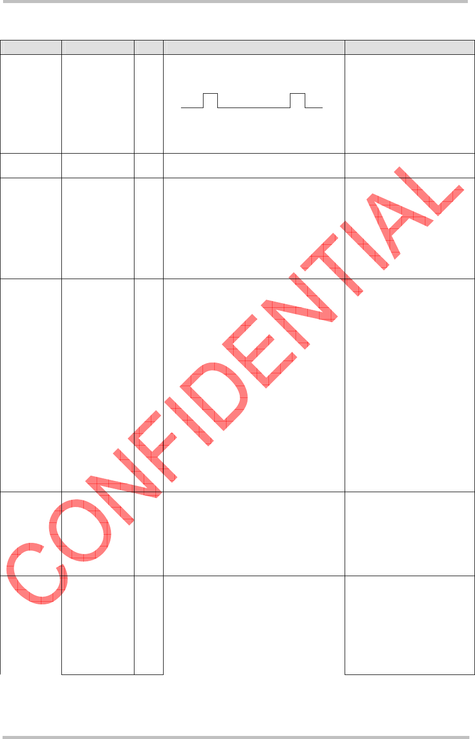
5.5. Pin Assignment and Signal Description
The board-to-board connector on HMS1 is an 80-pin double-row receptacle.
Figure 5: Pin assignments on board-to-board connector
1 GND GND 80
2 n.c. n.c. 79
3 n.c. PWR_IND 78
4 GND n.c. 77
5 n.c. n.c. 76
6 n.c. n.c. 75
7 n.c. GREEN 74
8 n.c. BLUE 73
9 n.c. n.c. 72
10 n.c. n.c. 71
11 n.c. n.c. 70
12 VUSB_IN USB_DP 69
13 n.c. USB_DN 68
14 n.c. n.c. 67
15 n.c. do not use 66
16 n.c. n.c. 65
17 n.c. n.c. 64
18 n.c. n.c. 63
19 n.c. n.c. 62
20 n.c. n.c. 61
21 GND n.c. 60
22 n.c. n.c. 59
23 n.c. n.c. 58
24 n.c. do not use 57
25 n.c. IGT 56
26 n.c. EMERG_RST 55
27 n.c. n.c. 54
28 n.c. n.c. 53
29 n.c. n.c. 52
30 n.c. n.c. 51
31 n.c. n.c. 50
32 n.c. n.c. 49
33 VDDLP n.c. 48
34 n.c. n.c. 47
35 n.c. VEXT 46
36 GND BATT+ 45
37 GND BATT+ 44
38 GND BATT+ 43
39 GND BATT+ 42
40 GND BATT+ 41
HMS1 Hardware Interface Description
Confidential / Preliminary s
HMS1_HD_V01.62 Page 28 of 39 2006-08-21
Table 10: Signal description
Function Signal name IO Signal form and level Comment
VBATT = 3.6V±5%
I ≈ 2A, during Tx burst (GSM)
Power
supply
BATT+ I
n Tx = n x 577µs peak current every
4.616ms
Five pins of BATT+ and GND
must be connected in parallel
for supply purposes because
higher peak currents may
occur.
Minimum voltage must not fall
below 3.3V including drop,
ripple, spikes.
Power
supply
GND Ground Application Ground
External
supply
voltage
VEXT O
Normal mode:
VOmin = 2.70V
VOtyp = 2.85V
VOmax = 3.00V
IOmax = Tbd.
VEXT may be used for
application circuits, for
example to supply power for
an SD card.
If unused keep pin open.
The external digital logic must
not cause any spikes or
glitches on voltage VEXT.
Power
indicator
PWR_IND O VIHmax = Tbd.
VOLmax = Tbd. at Imax = Tbd.
PWR_IND (Power Indicator)
notifies the module’s on/off
state.
PWR_IND is an open
collector that needs to be
connected to an external pull-
up resistor. Low state of the
open collector indicates that
the module is on. Vice versa,
high level notifies the Power-
down mode.
Therefore, the pin may be
used to enable external
voltage regulators which
supply an external logic for
communication with the
module, e.g. level converters.
Ignition IGT I
Internal pull-up: RI ≈ 200kΩ
VILmax = Tbd. at Imax = Tbd.
VOHmax = Tbd.
ON ~~~|____|~~~ Active Low ≥ 400ms
(to be verified)
This signal switches on the
module.
This line must be driven low
by an open drain or open
collector driver.
Emergency
reset
EMERG_RST I
Internal pull-up.
VILmax = 0.2V at Imax = -0.2mA
Signal ~~~|______|~~~ Pull down ≥ Tbd.
Reset in case of emergency.
This line must be driven low
by open drain or open
collector.
If unused keep pin open.

HMS1 Hardware Interface Description
Confidential / Preliminary s
HMS1_HD_V01.62 Page 29 of 39 2006-08-21
Function Signal name IO Signal form and level Comment
RTC backup VDDLP I RI ≈ 1kΩ
VBATT+ = 0V:
VI = 1.5V…3.25V at Imax= Tbd.
If unused keep pin open.
VUSB_IN I
VINmin = 3.2V
VINmax = 3.5V
USB
USB_DP
USB_DN
I/O Differential Output Crossover voltage
Range
VCRSmin = 1.3V, VCRSmax = 2.0V
Pullup at USB_DP Rtyp=1.5kOhm
All electrical characteristics
according to USB
Implementers’ Forum, USB
1.1 Full Speed Specification.

HMS1 Hardware Interface Description
Confidential / Preliminary s
HMS1_HD_V01.62 Page 30 of 39 2006-08-21
Function Signal name IO Signal form and level Comment
Status
Indication
BLUE
GREEN
O
O
VOHmin = BATT+ - 0.2V
VOLmax = Tbd.
IOmax = Tbd.
Signals can be used to
control LEDs via driving
transistors.
BLUE: “0” = module has been
registered to an UMTS cell.
GREEN: “0” = module has
been registered to a GSM
cell.
Constantly changing between
“0” and “1” = module is in
“network search” state.
CCRST O
RO ≈ 50Ω
VOLmax = 0.2V at I = 1mA
VOHmin = 2.7V at I = -1mA
VOHmax = 3.1V
CCIO I/O
RI ≈ 10kΩ
VILmax = 1V
VILmin = -0.3V
VIHmin = 1.9V
VIHmax = 3.2V
VOLmax = 0.2V at I = 1mA
VOHmin = 2.7V at I = -1mA
VOHmax = 3.1V
CCCLK O
RO ≈ 100Ω
VOLmax = 0.25V at I = 1mA
VOHmin = 2.65V at I = -1mA
VOHmax = 3.1V
SIM
interface
specified for
use with 3V
SIM card
CCVCC O
VOmin = 2.9V
VOtyp = 3V
VOmax = 3.1V
IOmax = -50mA
All signals of SIM interface
are protected against ESD
with a special diode array.
CCRST O
RO ≈ 50Ω
VOLmax = 0.2V at I = 1mA
VOHmin = 1.55V at I = -1mA
VOHmax = 1.85V
CCIO I/O
RI ≈ 10kΩ
VILmax = 0.6V
VILmin = -0.3V
VIHmin = 1.15V
VIHmax = 1.85V
VOLmax = 0.2V at I = 1mA
VOHmin = 1.5V at I = -1mA
VOHmax = 1.85V
CCCLK O
RO ≈ 100Ω
VOLmax = 0.25V at I = 1mA
VOHmin = 1.5V at I = -1mA
VOHmax = 1.85V
SIM
interface
specified for
use with
1.8V SIM
card
CCVCC O
VOmin = 1.74V
VOtyp = 1.8V
VOmax = 1.86V
IOmax = -50mA
All signals of SIM interface
are protected against ESD
with a special diode array.

HMS1 Hardware Interface Description
Confidential / Preliminary s
HMS1_HD_V01.62 Page 31 of 39 2006-08-21
5.6. Power Supply Ratings
Table 11: Power supply ratings
Parameter Description Conditions Min Typ Max Unit
Supply voltage Directly measured at reference points
Tbd. BATT+ and GND.
Voltage must stay within the min/max
values, including voltage drop, ripple,
spikes.
-5% 3.6 +5% V
Voltage drop during
transmit burst
Normal condition, power control level
for Pout max
400 mV
BATT+
Voltage ripple Normal condition, power control level
for Pout max
@ f<200kHz
@ f>200kHz
50
2
mV
mV
IVDDLP RTC Backup @ BATT+ = 0V Tbd. µA OFF State
supply current POWER DOWN mode Tbd. Tbd. µA
SLEEP mode @ DRX = 9 Tbd. mA
SLEEP mode @ DRX = 5 Tbd. mA
SLEEP mode @ DRX = 2 Tbd. mA
IBATT+
Average standby
supply current2)
IDLE mode @ DRX = 2 Tbd. mA

HMS1 Hardware Interface Description
Confidential / Preliminary s
HMS1_HD_V01.62 Page 32 of 39 2006-08-21
5.7. Air Interface
Test conditions: All measurements have been performed at Tamb= 25°C, VBATT+ nom = . The
reference points used on HMS1 are the BATT+ and GND contacts.
Table 12: Air Interface GSM
Parameter Min Typ Max Unit
GSM 850 824 849 MHz
E-GSM 900 880 915 MHz
GSM 1800 1710 1785 MHz
Frequency range
Uplink (MS → BTS)
GSM 1900 1850 1910 MHz
GSM 850 869 894 MHz
E-GSM 900 925 960 MHz
GSM 1800 1805 1880 MHz
Frequency range
Downlink (BTS → MS)
GSM 1900 1930 1990 MHz
GSM 850 31 33 35 dBm
E-GSM 9001 31 33 35 dBm
GSM 18002 28 30 32 dBm
RF power @ ARP with 50Ω load
GSM 1900 28 30 32 dBm
GSM 850 124
E-GSM 900 174
GSM 1800 374
Number of channels
GSM 1900 299
GSM 850 45 MHz
E-GSM 900 45 MHz
GSM 1800 95 MHz
Duplex spacing
GSM 1900 80 MHz
Carrier spacing 200 kHz
Multiplex, Duplex TDMA / FDMA, FDD
Time slots per TDMA frame 8
Frame duration 4.615 ms
Time slot duration 577 µs
Modulation GMSK
GSM 850 -102 -105.5 dBm
E-GSM 900 -102 -105.5 dBm
GSM 1800 -102 -105.5 dBm
Receiver input sensitivity @ ARP
BER Class II < 2.4% (static input level)
GSM 1900 -102 -105.5 dBm
1 Power control level PCL 5
2 Power control level PCL 0

HMS1 Hardware Interface Description
Confidential / Preliminary s
HMS1_HD_V01.62 Page 33 of 39 2006-08-21
Table 13: Air Interface UMTS
Parameter Min Typ Max Unit
UMTS Band I 1920 1980 MHz Frequency range
Uplink (MS → BTS)
UMTS Band I 2110 2170 MHz Frequency range
Downlink (BTS → MS)
UMTS Band I 21 24 25 dBm Max RF power @ ARP with 50Ω load
Power Class 3
UMTS Band I 190 MHz Duplex spacing
Channel raster 200 kHz
Duplex FDD
UMTS Band I -117 dBm/3,84 Mhz Receiver input sensitivity @ ARP
BER < 0,001 (static input level) DPCH_Ec
with 12,2 kbps reference channel
HMS1 Hardware Interface Description
Confidential / Preliminary s
HMS1_HD_V01.62 Page 34 of 39 2006-08-21
5.8. Electrostatic Discharge
The HSDPA engine is not protected against Electrostatic Discharge (ESD) in general.
Consequently, it is subject to ESD handling precautions that typically apply to ESD sensitive
components. Proper ESD handling and packaging procedures must be applied throughout
the processing, handling and operation of any application that incorporates a HMS1 module.
Special ESD protection provided on HMS1:
• Antenna interface: one discharge circuit
• SIM interface: serial resistor, clamp diodes for protection against over voltage.
• The remaining parts of HMS1 are not accessible to the user of the final product (since
they are installed within the device) and therefore, are only protected according to the
“Human Body Model” requirements.
HMS1 has been tested according to the EN 61000-4-2 standard. The measured values can
be gathered from the following table.
Table 14: Measured electrostatic values
Specification / Requirements Contact discharge Air discharge
CE ETS 300342-1 (June 1997)
ESD at SIM port ± 4kV ± 8kV
ESD at antenna port ± 4kV ± 8kV
ESD at 3.6V in, GND ± 4kV ± 8kV
Human Body Model (Test conditions: 1.5kΩ, 100pF)
ESD at SIM port ± 8kV ± 15kV
ESD at antenna port ± 8kV ± 15kV
ESD at 3.6V in, GND ± 8kV ± 15kV
Note: Please note that the values may vary with the individual application design. For
example, it matters whether or not the application platform is grounded over external
devices like a computer or other equipment, such as the Siemens reference
application described in Chapter 7.
HMS1 Hardware Interface Description
Confidential / Preliminary s
HMS1_HD_V01.62 Page 35 of 39 2006-08-21
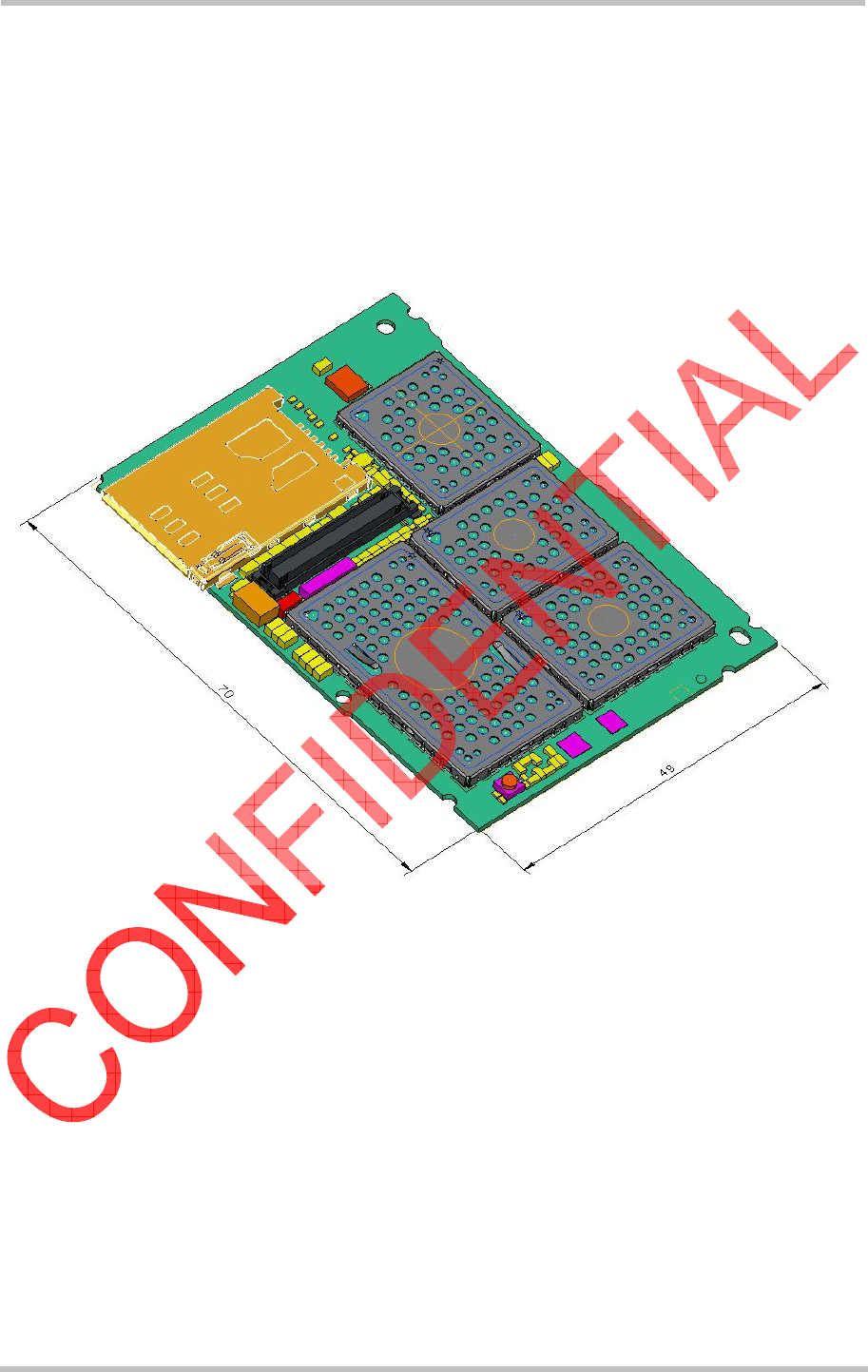
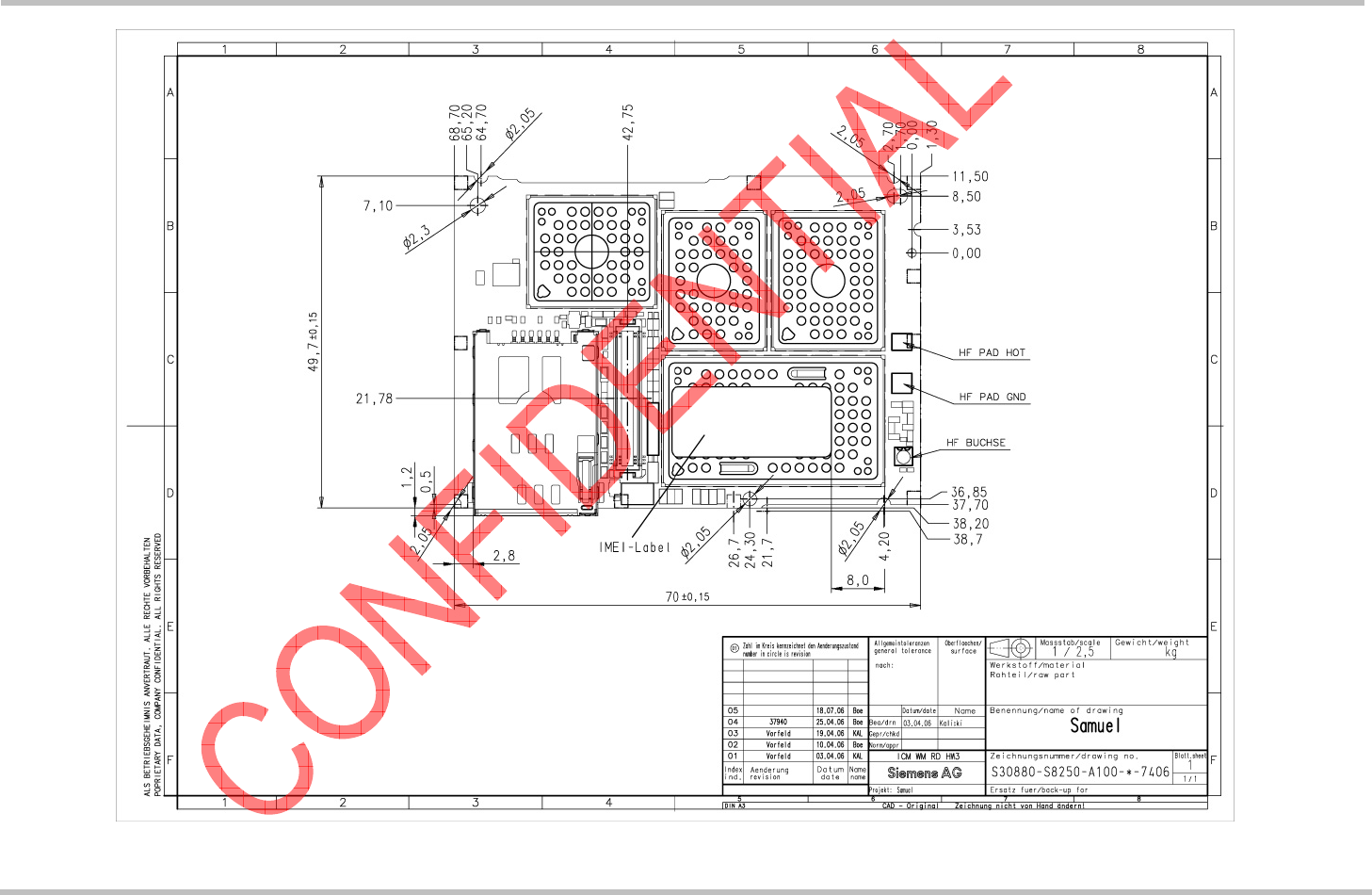
6. Mechanics
6.1. Mechanical Dimensions HMS1
The below figure shows the top view of HMS1 and provides an overview of the board's
mechanical dimensions.
Figure 6: HMS1 Top View (prelim.)
HMS1 Hardware Interface Description
Confidential / Preliminary s
HMS1_HD_V01.62 Page 36 of 39 2006-08-21
Figure 7: HMS1 Dimensions (prelim.)
HMS1 Hardware Interface Description
Confidential / Preliminary s
HMS1_HD_V01.62 Page 37 of 39 2006-08-21
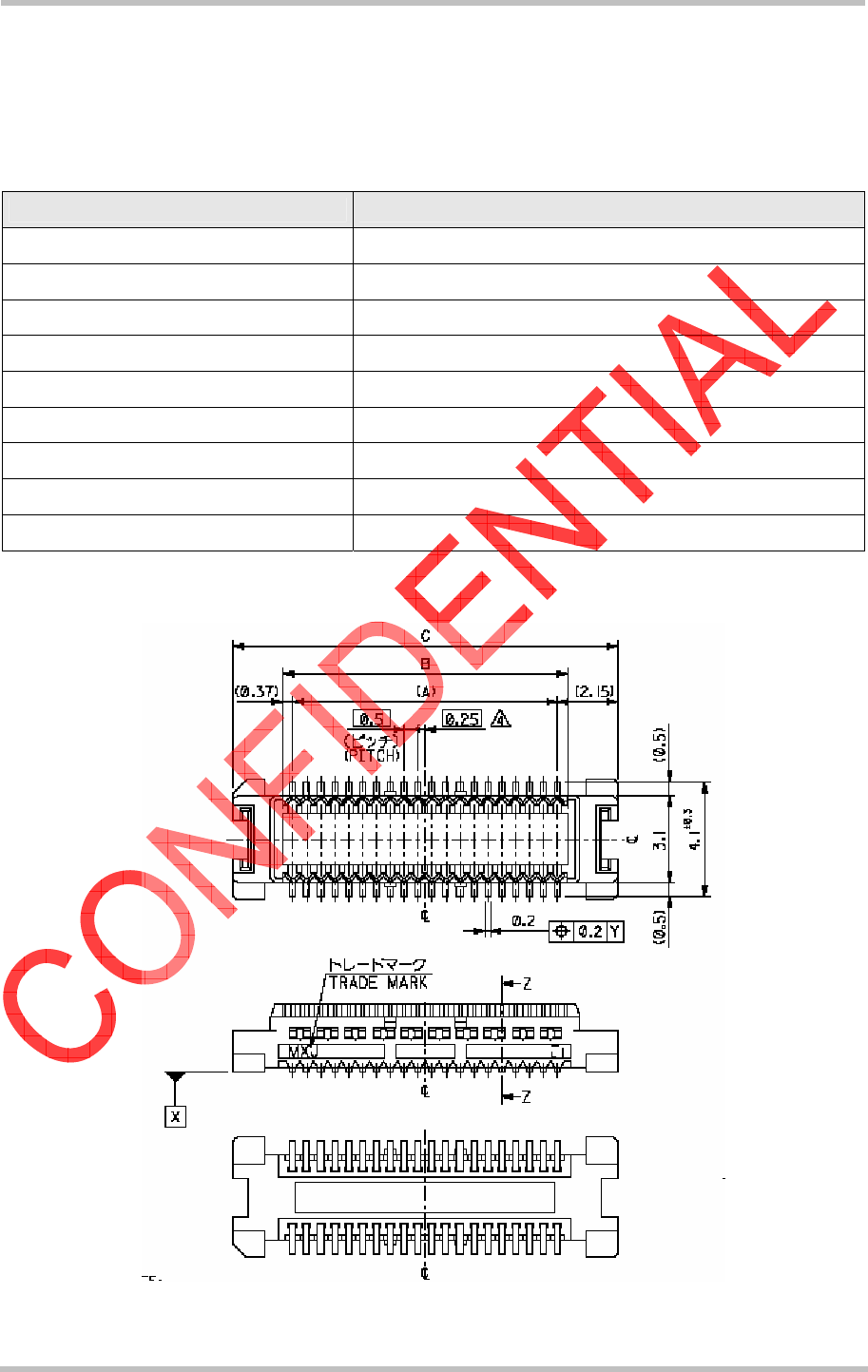
7. Board-to-Board Application Connector
This chapter provides specifications and handling instructions for the 80 pin board-to-board
application interface connector used to connect the HMS1 module to the host device.
Table 15: Electrical and mechanical characteristics of the 80 pin board-to-board connector
Parameter Specification (80-way connector)
Number of Contacts 80
Voltage 50V
Current Rating 0.5A max per contact
Resistance 0.05 Ohm per contact
Dielectric Withstanding Voltage 150V RMS AC for 1min
Operating Temperature -40°C...+125°C
Contact Material brass (CuZn)
Insulator Material LCP (= Liquid Crystal Polymer), glass-filled, white
Maximum connection cycles 20 (@ 50mOhm max)
The mechanical dimensions of the 80 pin board-to-board connector are shown below (as an
extract from the datasheet):
Figure 8: Mechanical dimensions of 80 pin board-to-board connector
HMS1 Hardware Interface Description
Confidential / Preliminary s
HMS1_HD_V01.62 Page 38 of 39 2006-08-21
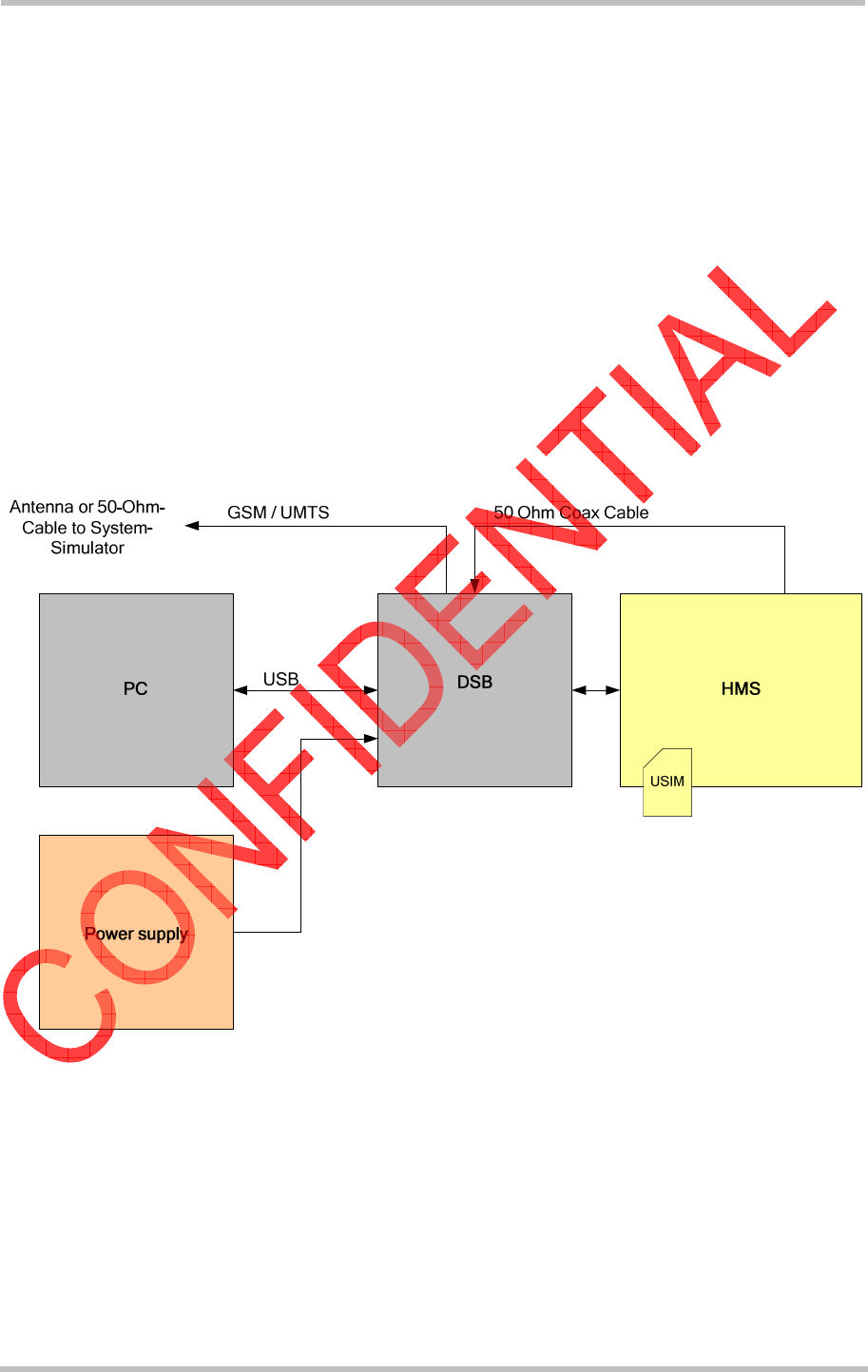
8. Reference Approval
8.1. Reference Equipment for Type Approval
The Siemens reference setup submitted to type approve HMS1 consists of the following
components:
• Siemens HMS1 cellular engine
• Development Support Box DSB
• SIM card reader integrated on the module
• U.FL-R-SMT antenna connector and U.FL-LP antenna cable
• PC as MMI
Figure 9: Reference equipment for Type Approval

HMS1 Hardware Interface Description
Confidential / Preliminary s
HMS1_HD_V01.62 Page 39 of 39 2006-08-21
8.2. Compliance with FCC Rules and Regulations
The FCC Equipment Authorization Certification for the HMS1 reference application described
in Section 8.1 is listed under the
FCC identifier QIPHMS1
IC: 267W-HMS1
granted to Siemens AG.
The HMS1 reference application registered under the above identifier is certified to be in
accordance with the following Rules and Regulations of the Federal Communications
Commission (FCC).
Power listed is ERP for Part 22 and EIRP for Part 24
“This device contains GSM, GPRS Class10 and EGPRS Class 10 functions in the 900
and 1800MHz Band and the WCDMA function in the FDD1 Band (2100MHz) which are
not operational in U.S. Territories.
This device is to be used only for mobile and fixed applications. The antenna(s) used
for this transmitter must be installed to provide a separation distance of at least 20 cm
from all persons and must not be co-located or operating in conjunction with any other
antenna or transmitter. Users and installers must be provided with antenna installation
instructions and transmitter operating conditions for satisfying RF exposure com-
pliance. Antennas used for this OEM module must not exceed 8.4dBi gain (GSM 1900)
and 2.9dBi (GSM 850) for mobile and fixed operating configurations. This device is
approved as a module to be installed in other devices.”
The FCC label of the module must be visible from the outside. If not, the host device is
required to bear a second label stating, “Contains FCC ID QIPHMS1”.
Manufacturers of mobile or fixed devices incorporating HMS1 modules are advised to include
instructions according to above mentioned RF exposure statements in their end product user
manual.
Please note that changes or modifications not expressly approved by the party responsible
for compliance could void the user’s authority to operate the equipment.
If the final product is not approved for use in U.S. territories the application manufacturer
shall take care that the 850 MHz and 1900 MHz frequency bands be deactivated and that
band settings be inaccessible to end users. If these demands are not met (e.g. if the AT
interface is accessible to end users), it is the responsibility of the application manufacturer to
always ensure that the application be FCC approved regardless of the country it is marketed
in.