THALES DIS AlS Deutschland PCS3 CDMA 1XRTT MODULE User Manual Rev
Gemalto M2M GmbH CDMA 1XRTT MODULE Rev
UserManual.wiki
>
THALES DIS AlS Deutschland
>
PCS3 User Manual
User Manual Rev
Navigation menu
Upload a User Manual
Namespaces
Wiki Guide
HTML
PDF
Info
Views
User Manual
Discussion / Help
Navigation
![PCS3_HD_v01.000-03 Confidential / Preliminary Page 9 of 101 2013-10-21 PCS3 Hardware Interface Description1 Introduction 1 Introduction The document1 describes the hardware of the PCS3 module, designed to connect to a cellular device application and the air interface. It helps you quickly retrieve interface specifications, electrical and mechanical details and information on the requirements to be considered for in- tegrating further components. 1.1 Related Documents [1] PCS3 AT Command Set [2] PCS3 Release Notes [3] DSB75 Support Box - Evaluation Kit for Cinterion Wireless Modules [4] Application Note 48: SMT Module Integration [5] Universal Serial Bus Specification Revision 2.0, April 27, 2000 1.2 Terms and Abbreviations Abbreviation Description ANSI American National Standards Institute AMR Adaptive Multi-rate ARP Antenna Reference Point BB Baseband BC Band Class BEP Bit Error Probability BTS Base Transceiver Station CB or CBM Cell Broadcast Message CDMA Code Division Multiple Access CE Conformité Européene (European Conformity) CS Coding Scheme CS Circuit Switched CSD Circuit Switched Data CTM Cellular Text Modem DAC Digital-to-Analog Converter DCS Digital Cellular System DL Download DRX Discontinuous Reception DSB Development Support Board 1. The document is effective only if listed in the appropriate Release Notes as part of the technical documentation delivered with your Cinterion Wireless Modules product.](https://usermanual.wiki/THALES-DIS-AlS-Deutschland/PCS3/User-Guide-2113265-Page-9.png)
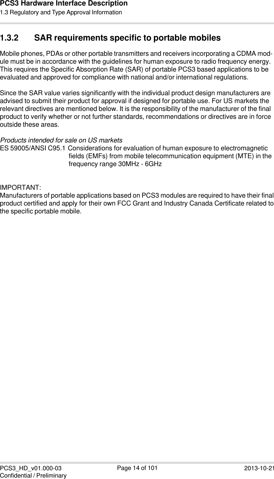
![PCS3_HD_v01.000-03 Confidential / Preliminary Page 18 of 101 2013-10-21 PCS3 Hardware Interface Description2.1 Key Features at a Glance Feature Implementation Interfaces Module interface Surface mount device with solderable connection pads (SMT application interface). Land grid array (LGA) technology ensures high solder joint reliability and provides the possibility to use an optional module mounting socket. For more information on how to integrate SMT modules see also [4]. This application note comprises chapters on module mounting and application layout issues as well as on additional SMT application development equipment. Antenna 50Ohms. CDMA main antenna USB USB 2.0 Full Speed (12Mbit/s) device interface Serial interface ASC0: • 8-wire modem interface with status and control lines, unbalanced,asynchronous • Adjustable baud rates from 1,200bps up to 921,600bps • Supports RTS0/CTS0 hardware flow control Status Signal line to indicate network connectivity state Audio 1 analog interface with microphone feeding 1 digital interface: PCM Power on/off, Reset Power on/off Switch-on by hardware signal IGT Switch-off by AT command (AT^SMSO) Automatic switch-off in case of critical temperature or voltage conditionsReset Orderly shutdown and reset by AT command Emergency-off Emergency-off by hardware signal EMERG_OFF if IGT is not active Special Features Phonebook Phone TTY/CTM support TTY only Antenna SAIC (Single Antenna Interference Cancellation) / DARP (Downlink Advanced Receiver Performance) Rx diversity (receiver type 3i - 16-QAM) Over-the-air provisioning Verizon specific OTASP (Over-the-Air Service Provisioning) and OTAPA (Over-the-Air Parameter Administration) Evaluation kit Evaluation module PCS3 module soldered onto a dedicated PCB that can be connected to an adapter in order to be mounted onto the DSB75. DSB75 DSB75 Development Support Board designed to test and type approve Cinterion Wireless Modules and provide a sample configuration for appli- cation engineering. A special adapter is required to connect the PCS3 evaluation module to the DSB75.](https://usermanual.wiki/THALES-DIS-AlS-Deutschland/PCS3/User-Guide-2113265-Page-18.png)
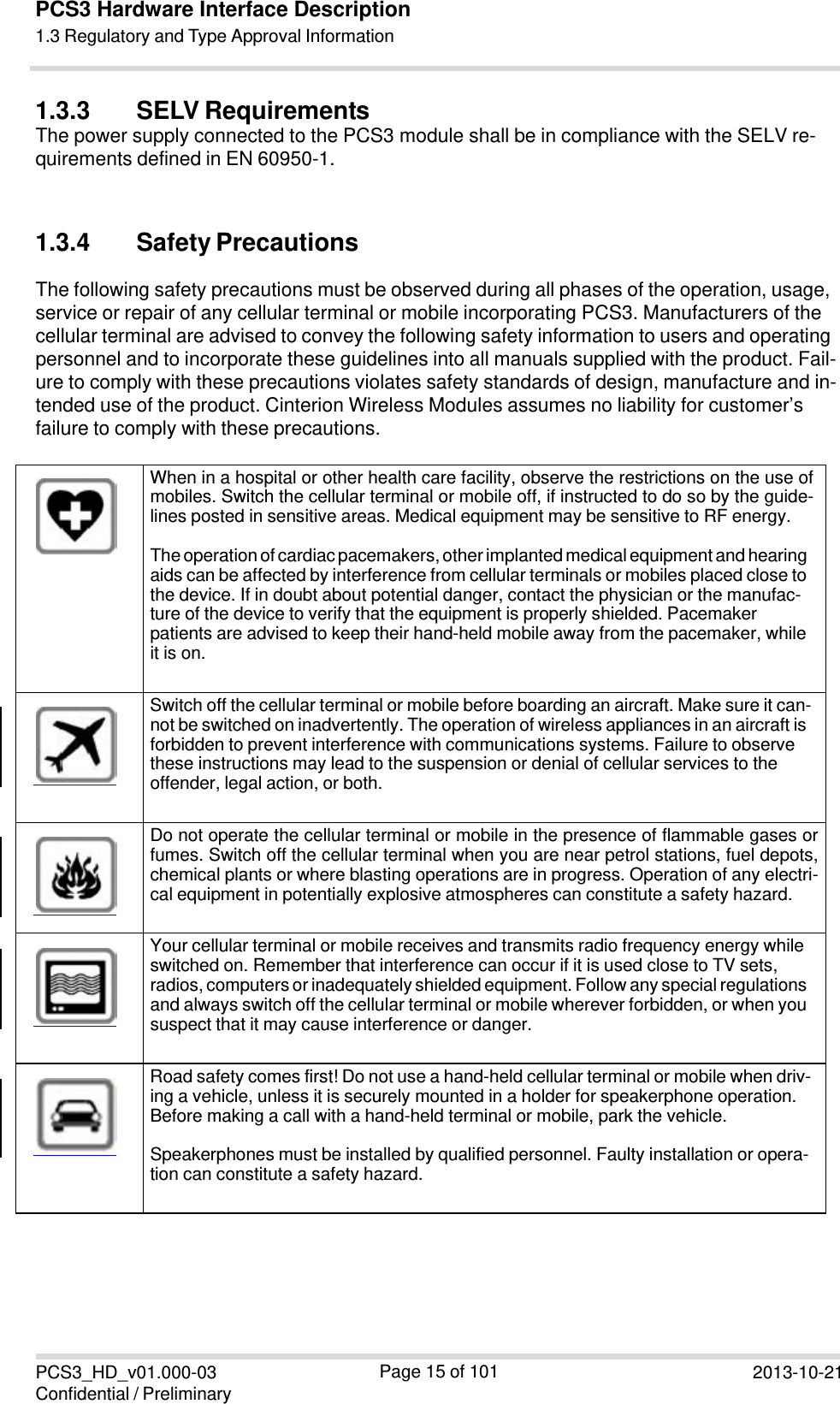
![PCS3_HD_v01.000-03 Confidential / Preliminary Page 22 of 101 2013-10-21 PCS3 Hardware Interface Description3.1 Operating Modes 3.1 Operating Modes The table below briefly summarizes the various operating modes referred to in the following chapters. Table 6: Overview of operating modes Mode Function Normal operation CDMA SLEEP Power saving set automatically when no call is in progress and the USB connection is suspended by host or not present and no active commu- nication via ASC0. CDMA IDLE Power saving disabled (see [1]: AT^SCFG "MEopMode/ PwrSave",<PwrSaveMode>) or an USB connection not suspended, but no call in progress. CDMA TALK/ CDMA DATA CDMA data transfer in progress. Power consumption depends on net- work settings and data transfer rate. Power Down Normal shutdown after sending the AT^SMSO command. Only a voltage regulator is active for powering the RTC. Software is not active. Interfaces are not accessible. Operating volt- age (connected to BATT+) remains applied. Airplane mode Airplane mode shuts down the radio part of the module, causes the module to log off from the CDMA network and disables all AT commands whose execution requires a radio con- nection. Airplane mode can be controlled by AT command (see [1]).](https://usermanual.wiki/THALES-DIS-AlS-Deutschland/PCS3/User-Guide-2113265-Page-22.png)
![PCS3_HD_v01.000-03 Confidential / Preliminary Page 29 of 101 2013-10-21 PCS3 Hardware Interface Description3.3 Power-Up / Power-Down Scenarios 3.3.5 Automatic Shutdown Automatic shutdown takes effect if: • The PCS3 board is exceeding the critical limits of overtemperature or undertemperature • Undervoltage or overvoltage is detected The automatic shutdown procedure is equivalent to the power down initiated with the AT^SMSO command, i.e. PCS3 logs off from the network and the software enters a secure state avoiding loss of data. Alert messages transmitted before the device switches off are implemented as Unsolicited Re- sult Codes (URCs). The presentation of the temperature URCs can be enabled or disabled with the AT commands AT^SCTM. The URC presentation mode varies with the condition, please see Section 3.3.5.1 to Section 3.3.5.3 for details. For further instructions on AT commands refer to [1].](https://usermanual.wiki/THALES-DIS-AlS-Deutschland/PCS3/User-Guide-2113265-Page-29.png)
![PCS3_HD_v01.000-03 Confidential / Preliminary Page 30 of 101 2013-10-21 PCS3 Hardware Interface Description3.3 Power-Up / Power-Down Scenarios 3.3.5.1 Thermal Shutdown The board temperature is constantly monitored by an internal NTC resistor located on the PCB. The values detected by the NTC resistor are measured directly on the board and therefore, are not fully identical with the ambient temperature. Each time the board temperature goes out of range or back to normal, PCS3 instantly displays an alert (if enabled). • URCs indicating the level "1" or "-1" allow the user to take appropriate precautions, such as protecting the module from exposure to extreme conditions. The presentation of the URCs depends on the settings selected with the AT^SCTM write command: AT^SCTM=1: Presentation of URCs is always enabled. AT^SCTM=0 (default): Presentation of URCs is enabled during the 15 second guard period after start-up of PCS3. After expiry of the 15 second guard period, the presentation will be disabled, i.e. no URCs with alert levels "1" or ''-1" will be generated. • URCs indicating the level "2" or "-2" are instantly followed by an orderly shutdown. The pre- sentation of these URCs is always enabled, i.e. they will be output even though the factory setting AT^SCTM=0 was never changed. The maximum temperature ratings are stated in Section 6.2. Refer to Table 8 for the associated URCs. Table 8: Temperature dependent behavior Sending temperature alert (15sec after PCS3 start-up, otherwise only if URC presentation enabled) ^SCTM_B: 1 Caution: Board close to over temperature limit, i.e., board is 5°C below over temperature limit. ^SCTM_B: -1 Caution: Board close to under temperature limit, i.e., board is 5°C above under- temperature limit. ^SCTM_B: 0 Board back to uncritical temperature range, i.e., board is 6°C below its over- or above its under temperature limit. Automatic shutdown (URC appears no matter whether or not presentation was enabled) ^SCTM_B: 2 Alert: Board equal or beyond over temperature limit. PCS3 switches off. ^SCTM_B: -2 Alert: Board equal or below under temperature limit. PCS3 switches off. The AT^SCTM command can also be used to check the present status of the board. Depending on the selected mode, the read command returns the current board temperature in degrees Celsius or only a value that indicates whether the board is within the safe or critical temperature range. See [1] for further instructions.](https://usermanual.wiki/THALES-DIS-AlS-Deutschland/PCS3/User-Guide-2113265-Page-30.png)
![PCS3_HD_v01.000-03 Confidential / Preliminary Page 33 of 101 2013-10-21 PCS3 Hardware Interface Description3.4 Power Saving 3.4 Power Saving PCS3 is able to reduce its functionality to a minimum (during the so-called SLEEP mode) in order to minimize its current consumption. The following sections explain the module’s CTS0 behavior and also mention how to wake up from or disable the so-called SLEEP mode. The implementation of the USB host interface also influences the module’s power saving behavior and therefore its current consumption. For more information see Section 3.6. Note. The module’s SLEEP mode current consumption can be reduced significantly (0.8mA) by enabling the VEXT power save mode. Hence, it is recommended to enable power saving on VEXT if at all possible. For more information see Table 22: VEXT. Another feature influencing the current consumption is the configuration of the GNSS antenna interface. For details see Section 6.9. 3.4.1 Power Saving while Attached to CDMA Networks The so-called slotted paging in CDMA is similar to the WCDMA paging timing cycles for power saving. During normal CDMA operation, i.e., the module is connected to a CDMA network, the duration of a power saving period varies. It may be calculated using the following formula: T=2i * 1.28s (16 slots of 80ms) The slot cycle index i is determined by the CDMA network and can be an integer between -4 to 7 inclusive. The typical value is 2. Therefore, the typical power saving period would be (22)*1.28s = 5.12s. 3.4.2 Timing of the CTS0 Signal, CDMA As long as PCS3 is operated via the ASC0 interface and not in power saving mode, the CTS0 line is always active. This means that while attached to a network the CTS0 signal will be tem poraly active during each paging. After a concluding activity on the serial interface ASC0 - and depending on the module’s other activities - it takes by default 5 seconds before CTS0 goes inactive (again) and power saving starts. The 5 second delay period can be configured using the AT^SCFG parameter "MEop- Mode/PwrSave", <PwrSaveDelay> (see [1]). With regard to programming or using timeouts, the UART must take the varying CTS0 inactivity periods into account. Note: Hardware handshaking is mandatory if employing PCS3’s ASC0 interface with enabled power saving. Thus AT commands are only recognized by the module while CTS0 is active.](https://usermanual.wiki/THALES-DIS-AlS-Deutschland/PCS3/User-Guide-2113265-Page-33.png)
![PCS3_HD_v01.000-03 Confidential / Preliminary Page 34 of 101 2013-10-21 PCS3 Hardware Interface Description3.4 Power Saving 3.4.3 Wake up from or Disabling Power Saving The RTS0 line can be used to wake up the module from its power saving SLEEP mode. RTS0 activation (high to low transition) may be employed to cut short pauses between listening to paging messages. Following an RTS toggle the module will return to SLEEP mode 5 seconds after the last character was sent over the interface. This default delay period can be configured using the AT^SCFG parameter "MEopMode/PwrSave", <PwrSaveDelay>. If not regularly woken up from power saving (through network requirements or by means of RTS toggling as described above), the power saving timeout recommended for the AT^SCFG parameter "MEopMode/PwrSave", <PwrSaveTimeout> ensures that the module regularly wakes up from its power saving state (SLEEP mode). It is recommended to configure a regular module wake up, especially if the radio interface is switched off (Airplane mode) and the mod- ule is connected via serial interface (i.e., AT^SDPORT=2) to an external application without di- rect access to its RTS0 line (e.g., an application using standard Windows/Linux serial device drivers). The AT^SCFG parameter "MEopMode/PwrSave", <PwrSaveMode> can be used to disable power saving completely, i.e., the module will no longer enter SLEEP mode but remain in IDLE mode instead. Please note that if this setting is used to avoid implementing hardware hand- shaking on ASC0, it is mandatory to have RTS0 pulled down or left open (an internal pull down is available). For more information on power saving and the appropriate AT^SCFG parameters to configure the power save behavior see [1].](https://usermanual.wiki/THALES-DIS-AlS-Deutschland/PCS3/User-Guide-2113265-Page-34.png)
![PCS3_HD_v01.000-03 Confidential / Preliminary Page 37 of 101 2013-10-21 PCS3 Hardware Interface Description3.6 USB Interface 3.6.1 Reducing Power Consumption While a USB connection is active, the module will never switch into SLEEP Mode. Only if the USB interface is in Suspended state or Detached (i.e., VUSB_IN = 0) is the module able to switch into SLEEP mode thereby saving power. There are two possibilities to enable power re- duction mechanisms: • Recommended implementation of USB Suspend/Resume/Remote Wakeup: The USB host should be able to bring its USB interface into the Suspended state as described in the “Universal Serial Bus Specification Revision 2.0“1. For this functionality to work, the VUSB_IN line should always be kept enabled. On incoming calls and other events PCS3 will then generate a Remote Wakeup request to resume the USB host controller. See also [5] (USB Specification Revision 2.0, Section 10.2.7, p.282): "If USB System wishes to place the bus in the Suspended state, it commands the Host Con- troller to stop all bus traffic, including SOFs. This causes all USB devices to enter the Sus- pended state. In this state, the USB System may enable the Host Controller to respond to bus wakeup events. This allows the Host Controller to respond to bus wakeup signaling to restart the host system." • Implementation for legacy USB applications not supporting USB Suspend/Resume: As an alternative to the regular USB suspend and resume mechanism it is possible to employ the RING0 or WAKEUP line to wake up the host application in case of incoming calls or events signalized by URCs while the USB interface is in Detached state (i.e., VUSB_IN = 0). Every wakeup event will force a new USB enumeration. Therefore, the external application has to carefully consider the enumeration timings to avoid loosing any signalled events. For details on this host wakeup functionality see Section 3.10.4. 1. The specification is ready for download on http://www.usb.org/developers/docs/](https://usermanual.wiki/THALES-DIS-AlS-Deutschland/PCS3/User-Guide-2113265-Page-37.png)
![PCS3_HD_v01.000-03 Confidential / Preliminary Page 38 of 101 2013-10-21 PCS3 Hardware Interface Description3.7 Serial Interface ASC0 3.7 Serial Interface ASC0 PCS3 offers an 8-wire unbalanced, asynchronous modem interface ASC0 conforming to ITU- T V.24 protocol DCE signalling. The electrical characteristics do not comply with ITU-T V.28. The significant levels are 0V (for low data bit or active state) and 1.8V (for high data bit or in- active state). For electrical characteristics please refer to Table 22. For an illustration of the in- terface line’s startup behavior see Section 3.10.6. PCS3 is designed for use as a DCE. Based on the conventions for DCE-DTE connections it communicates with the customer application (DTE) using the following signals: • Port TXD @ application sends data to the module’s TXD0 signal line • Port RXD @ application receives data from the module’s RXD0 signal line Figure 10: Serial interface ASC0 Features: • Includes the data lines TXD0 and RXD0, the status lines RTS0 and CTS0 and, in addition, the modem control lines DTR0, DSR0, DCD0 and RING0. • ASC0 is designed for controlling voice calls, transferring data and for controlling the module with AT commands. • Full multiplexing capability allows the interface to be partitioned into virtual channels. • The RING0 signal serves to indicate incoming calls and other types of URCs (Unsolicited Result Code). It can also be used to send pulses to the host application, for example to wake up the application from power saving state. See [1] for details on how to configure the RING0 line by AT^SCFG. • Configured for 8 data bits, no parity and 1 stop bit. • ASC0 can be operated at fixed bit rates from 9600bps up to 921600bps. • Supports RTS0/CTS0 hardware flow control. • Wake up from SLEEP mode by RTS0 activation (high to low transition). Note. If the ASC0 serial interface is the application’s only interface, it is suggested to connect test points on the USB signal lines as a potential tracing possibility.](https://usermanual.wiki/THALES-DIS-AlS-Deutschland/PCS3/User-Guide-2113265-Page-38.png)
![PCS3_HD_v01.000-03 Confidential / Preliminary Page 40 of 101 2013-10-21 PCS3 Hardware Interface Description3.8 Analog Audio Interface 3.8 Analog Audio Interface PCS3 has an analog audio interface with a balanced analog microphone input and a balanced analog earpiece output. A supply voltage and an analog ground connection are provided at dedicated lines. PCS3 offers eight audio modes which can be selected with the AT^SNFS command. The elec- trical characteristics of the voiceband part vary with the audio mode. For example, sending and receiving amplification, sidetone paths, noise suppression etc. depend on the selected mode and can in parts be altered with AT commands (except for mode 1). Please refer to Section 6.7 for specifications of the audio interface and an overview of the audio parameters. Detailed instructions on using AT commands are presented in [1]. Table 25 sum- marizes the characteristics of the various audio modes and shows what parameters are sup- ported in each mode. When shipped from factory, all audio parameters of PCS3 are set to audio mode 1. This is the default configuration optimized for the Votronic HH-SI-30.3/V1.1/0 handset and used for type approving the Cinterion Wireless Modules reference configuration. Audio mode 1 has fix pa- rameters which cannot be modified. To adjust the settings of the Votronic handset simply change to another audio mode.](https://usermanual.wiki/THALES-DIS-AlS-Deutschland/PCS3/User-Guide-2113265-Page-40.png)
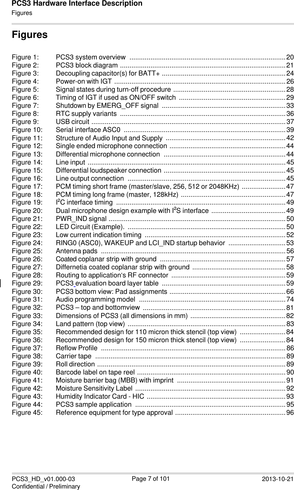
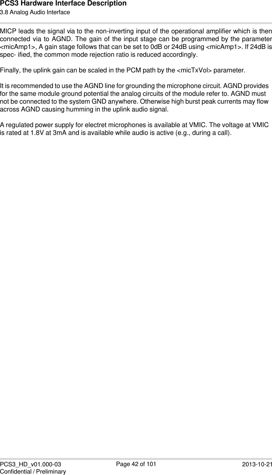
![PCS3_HD_v01.000-03 Confidential / Preliminary Page 41 of 101 2013-10-21 PCS3 Hardware Interface Description3.8 Analog Audio Interface 3.8.1 Microphone Inputs and Supply The differential microphone inputs MICP and MICN present variable impedances depending on the gain. The microphone inputs must be decoupled by capacitors Ck (typical 1µF). The in- put stage uses a differential operational amplifier circuit with programmable resistors in the in- put and the feedback path. The detailed structure of this stage and the following uplink path is shown in Figure 11. The input can be controlled by the AT command AT^SNFI. Command pa- rameters with their effect are mentioned in the figure and marked in <red>. More information about audio AT commands can be found in Section 6.7 and [1]. Module Rs VMIC Ck MICN <micAmp1> 0dBm or 24dBm VMIC AGND - A PCM X Ck MICP Rs AGND AGND D <micTxVol> GND GND Line leading burst current GND V Noise Application GND Connection Resistance Figure 11: Structure of Audio Input and Supply](https://usermanual.wiki/THALES-DIS-AlS-Deutschland/PCS3/User-Guide-2113265-Page-41.png)
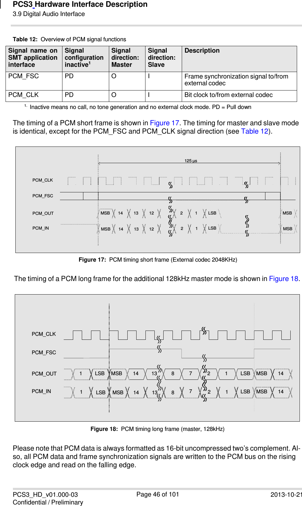
![PCS3_HD_v01.000-03 Confidential / Preliminary Page 45 of 101 2013-10-21 PCS3 Hardware Interface Description3.9 Digital Audio Interface 3.9 Digital Audio Interface PCS3 supports a digital audio interface that can be employed either as pulse code modulation (see Section 3.9.1) or as inter IC sound interface (see Section 3.9.2). Operation of these inter- face variants is mutually exclusive. 3.9.1 Pulse Code Modulation Interface (PCM) PCS3’s PCM interface can be used to connect audio devices capable of pulse code modula- tion. The PCM functionality allows the use of a codec like the Freescale MC145483. Using the AT^SAIC command you can activate and configure the PCM interface (see [1]). The PCM interface supports the following modes: • Master mode, slave mode • Short frame synchronization • 256kHz, 512kHz and 2048kHz bit clock • Additional master mode with 128kHz, long frame synchronization For the PCM interface configuration the parameters <clock>, <mode> <frame_mode> and <ext_clk_mode> of the AT^SAIC command can be configured. The following table lists possi- ble combinations: Table 11: Configuration combinations for the PCM interface Configuration <clock> <mode> <frame_mode> <ext_clk_mode> Master, 128kHz, long frame 0 0 1 0 or 1 Master, 256kHz, short frame 1 0 0 0 or 1 Master, 512kHz, short frame 2 0 0 0 or 1 Master, 2048kHz, short frame 3 0 0 0 or 1 Slave, 256kHz, short frame 1 1 0 1 Slave, 512kHz, short frame 2 1 0 1 Slave, 2048kHz, short frame 3 1 0 1 In slave mode <clock> must be set according the source clock frequency. Being in master mode clock and frame synchronization signals may be permanently switched on by <ext_clk_mode> parameter. These signals may be used for clocking digital audio periphery outside a call. Table 12 lists the available PCM interface signals. Table 12: Overview of PCM signal functions Signal name on SMT application interface Signal configuration inactive1 Signal direction: Master Signal direction: Slave Description PCM_OUT PD O O PCM Data from PCS3 to external codec PCM_IN PD I I PCM Data from external codec to PCS3](https://usermanual.wiki/THALES-DIS-AlS-Deutschland/PCS3/User-Guide-2113265-Page-45.png)
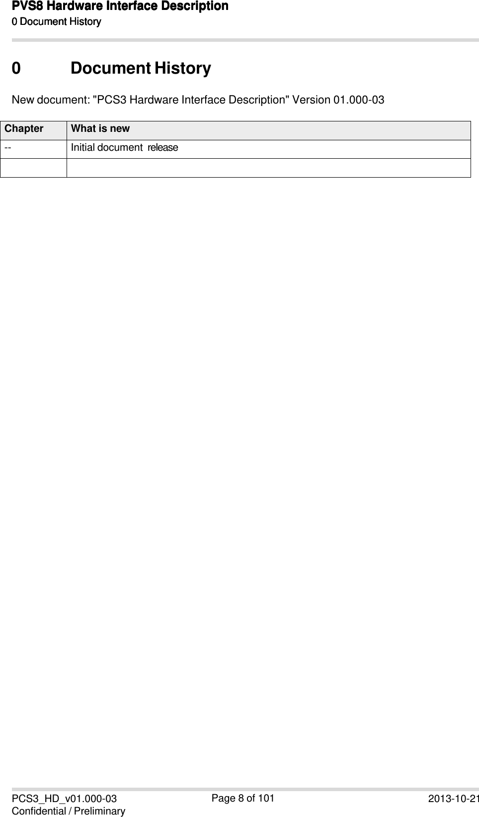
![PCS3_HD_v01.000-03 Confidential / Preliminary Page 48 of 101 2013-10-21PCS3 Hardware Interface Description3.10 Control Signals SMT interface 3.10 Control Signals 3.10.1 PWR_IND Signal PWR_IND notifies the on/off state of the module. High state of PWR_IND indicates that the module is switched off. The state of PWR_IND immediately changes to low when IGT is pulled low. For state detection an external pull-up resistor is required. Module e.g. BATT+ Power supply On/Off PWR_IND (open drain driver) Figure 21: PWR_IND signal 3.10.2 Network Connectivity Status Signals The STATUS line serves to indicate the module’s network connectivity state and can be used to control an externally connected LED as shown in Figure 22. To operate the LED a buffer, e.g. a transistor or gate, must be included in the external application. VCC LED STATUS 0 = LED off 1 = LED on GND Figure 22: LED Circuit (Example) For electrical characteristics of the STATUS line see Table 22. The network connectivity signal function is volatile and has to be activated after module startup with AT^SLED. For details on the command as well as status and mode indications through blinking intervals see [1].](https://usermanual.wiki/THALES-DIS-AlS-Deutschland/PCS3/User-Guide-2113265-Page-48.png)
![PCS3_HD_v01.000-03 Confidential / Preliminary Page 49 of 101 2013-10-21PCS3 Hardware Interface Description3.10 Control Signals 3.10.3 Behavior of the RING0 Line (ASC0 Interface only) The RING0 line is available on the first serial interface ASC0 (see also Section 3.7). The signal serves to indicate incoming calls and other types of URCs (Unsolicited Result Code). Although not mandatory for use in a host application, it is strongly suggested that you connect the RING0 line to an interrupt line of your application. In this case, the application can be de- signed to receive an interrupt when a falling edge on RING0 occurs. This solution is most ef- fective, particularly, for waking up an application from power saving. Note that if the RING0 line is not wired, the application would be required to permanently poll the data and status lines of the serial interface at the expense of a higher current consumption. Therefore, utilizing the RING0 line provides an option to significantly reduce the overall current consumption of your application. The RING0 line behavior and usage can be configured by AT command. For details see [1]: AT^SCFG. 3.10.4 Host Wakeup If no call, data or message transfer is in progress, the host may shut down its own USB inter- face to save power. If a call or other request (URC) arrives, the host can be notified of this event and be woken up again by a state transition of either the RING0 or the WAKEUP line. This func- tionality should only be used with legacy USB applications not supporting the recommended USB suspend and resume mechanism as described in in the “Universal Serial Bus Specifica- tion Revision 2.0“1 (see also Section 3.6.1). The behaviour of these RING0 or WAKEUP lines as host wakeup line has to be enabled and configured by AT command (see [1]: AT^SCFG). Possible states are listed in Table 14. Please note that it is not possible to use both lines in parallel. The WAKEUP signal just inverts the RING0 signal in order to meet different application needs. Table 14: Host wakeup lines Signal I/O Description RING0 O Inactive to active low transition: 0 = The host shall wake up 1 = No wake up request WAKEUP O Inactive to active high transition: 0 = No wake up request 1 = The host shall wake up 1. The specification is ready for download on http://www.usb.org/developers/docs/](https://usermanual.wiki/THALES-DIS-AlS-Deutschland/PCS3/User-Guide-2113265-Page-49.png)
![PCS3_HD_v01.000-03 Confidential / Preliminary Page 50 of 101 2013-10-21PCS3 Hardware Interface Description3.10 Control Signals 3.10.5 Low Current Indicator A low current indication is optionally available over the LC_IND line. By default, low current in- dication is disabled. For the LC_IND signal to work as a low current indicator the feature has to be enabled by AT command (see [1]: AT^SCFG: MEopMode/PowerMgmt/LCI). If enabled, the LC_IND signal is high when the module is sleeping. During its sleep the module will for the most part be slow clocked with 32kHz RTC. Table 15: Low current indicator line Signal I/O/P Description LC_IND O Inactive to active high transition: 0 = High current consumption The module draws its power via BATT+ 1 = Low current consumption (only reached during SLEEP mode) The module draws only a low current via BATT+ LC_IND 1 0 t IBATT+ tLC ILCpk (typ. 150mA) ILCmax <100mA tLCpk<100µs tLCru> t 300µs Figure 23: Low current indication timing tLC Time for the IBATT+ current consumption: ILCmax<100mA. tLCpk Max. time duration for the inrush current peak at the end of the low current period. tLCru When the LC_IND signal becomes inactive (low) the current ramps up to the maximum low current value within tLCru. ILCpk When the module turns from sleep to normal operation some internal supply voltages will be switched on. That causes a small inrush current peak. ILCmax During the low current period tLC the current consumption does not exceed the ILCmax value.](https://usermanual.wiki/THALES-DIS-AlS-Deutschland/PCS3/User-Guide-2113265-Page-50.png)
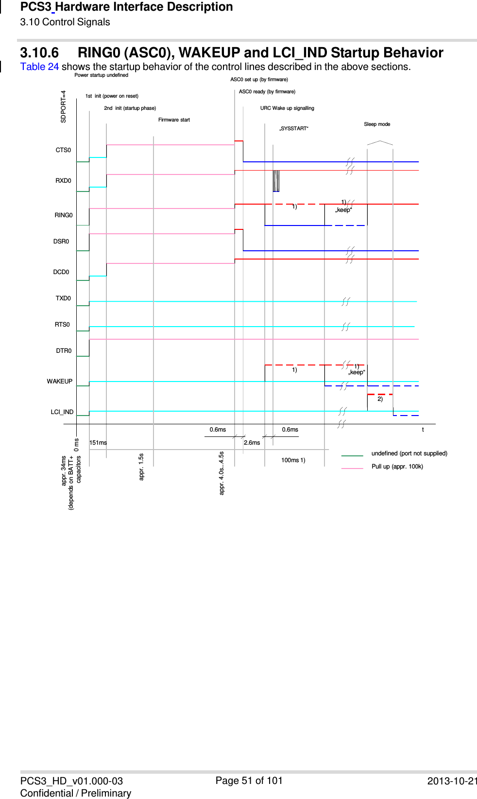
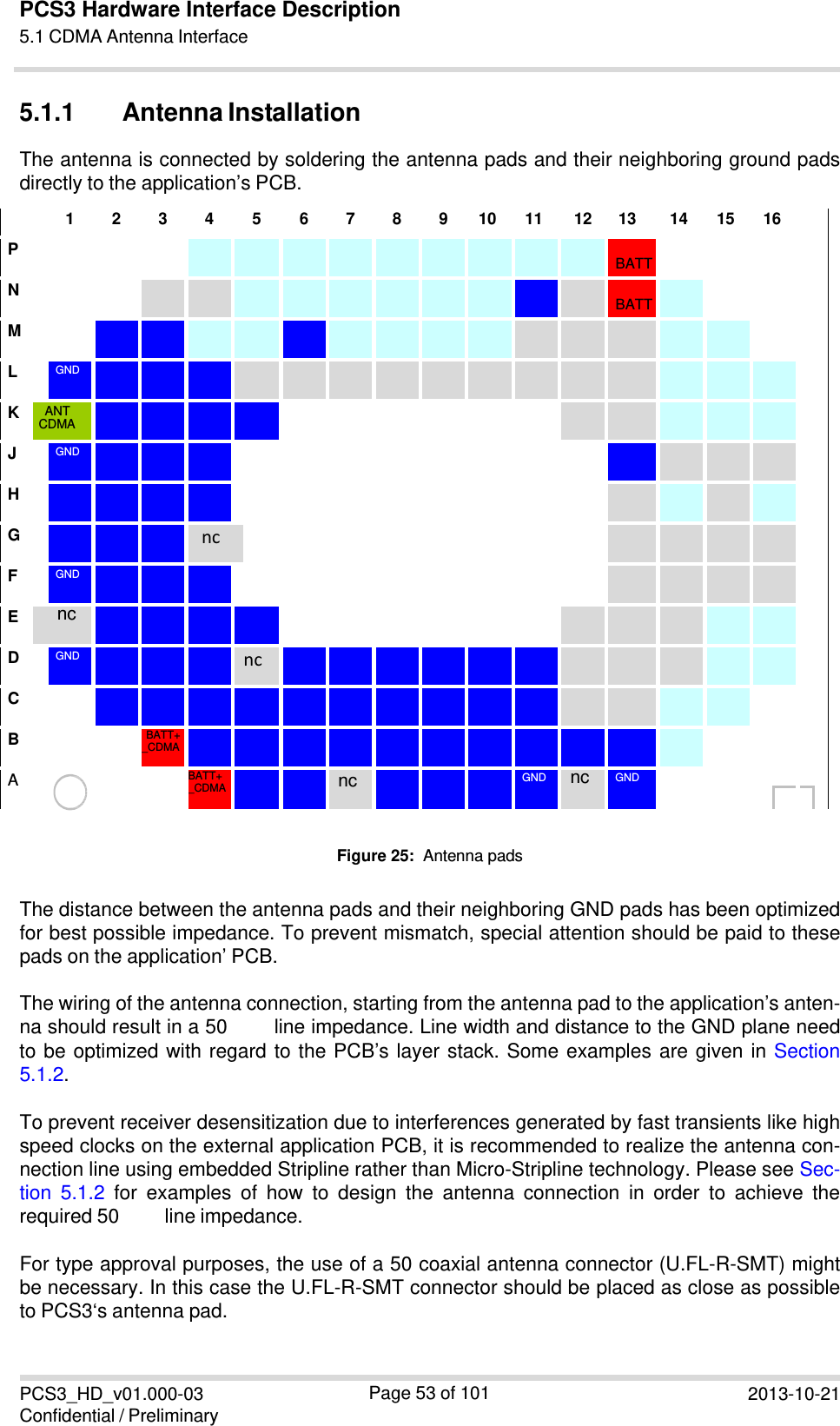
![PCS3_HD_v01.000-03 Confidential / Preliminary Page 52 of 101 2013-10-21 PCS3 Hardware Interface Description5 Antenna Interfaces Configuration Wakeup State RING0 WAKEUP AT^SCFG="URC/Ringline","local" (P) low (active) low (PD) "asc0" low (active) low (PD) "off" high low (PD) "wakeup" high high (active)Configuration Wakeup Active Time for RING0, WAKEUP AT^SCFG="URC/Ringline/ActiveTime","0" 4.6ms-9ms "1" (P) 100ms "2" 1s "keep" keeps active until 1st time enter sleep modePull down (appr. 100k)iven high driven low dashed line: lternative funtion 1) (P) Power up default value 2) If needed: During runtime the LCI feature has to be enabled by AT^SCFG="MEopMode/PowerMgmt/LCI","enabled" Figure 24: RING0 (ASC0), WAKEUP and LCI_IND startup behavior 4 Antenna Interfaces The PCS3 only CDMA main Antenna, PCS3 didn’t have GPS fora GNSS receiver 5.1 CDMA Antenna Interface The PCS3 CDMA antenna interface comprises a main CDMA antenna as well as an optional CDMA Rx diversity antenna to improve signal reliability and quality1. The interface has an impedance of 50ohm PCS3 is capable of sustaining a total mismatch at the antenna interface without any damage, even when transmitting at maximum RF power. The external antenna must be matched properly to achieve best performance regarding radiation power, modulation accuracy and harmonic suppression. Matching networks are not included on the PCS3 PCB and should be placed in the host application, if the antenna does not have an impedance of 50ohm Regarding the return loss PCS3 provides the following values in the active band: Table 16: Return loss in the active band State of module Return loss of module Recommended return loss of application Receive > 8dB > 12dB Transmit not applicable > 12dB Idle < 5dB not applicable 1. By delivery default the optional CDMA Rx diversity antenna is configured as available for the module. To avoid negative side effects and performance degradation it is recommended to disable the diversity an- tenna path if - the host application does not support a diversity antenna - the host application includes a diversity antenna - but a network simulator is used for development and performance tests. Please refer to [1] for details on how to configure antenna settings.](https://usermanual.wiki/THALES-DIS-AlS-Deutschland/PCS3/User-Guide-2113265-Page-52.png)
![PCS3 Hardware Interface Description6.5 Pad Assignment and Signal Description PCS3_HD_v01.000 Confidential / Preliminary Page 68 of 101 2013-10-21Please note that the reference voltages listed in Table 22 are the values measured directly on the PCS3 module. They do not apply to the accessories connected. Table 22: Signal description Function Signal name IO Signal form and level Comment Power supply BATT+_CDMA BATT+_CDMA I VImax = 4.2V VInorm = 3.8V VImin = 3.3V during Tx burst on board Imax 800mA, during Tx burst Lines of BATT+ and GND must be connected in paral- lel for supply purposes because higher peak cur- rents may occur. Minimum voltage must not fall below 3.3V including drop, ripple, spikes. BATT+ I VImax = 4.2V VInorm = 3.8V VImin = 3.3V during Tx burst on board Imax = 250mA Power supply GND Ground Application Ground External supply voltage VEXT O CLmax = 1µF High power mode: VO = 1.80V +1% -5% IOmax = -50mA Power save mode: VO = 1.80V +2% -5% IOmax = -10mA VEXT may be used for application circuits. Not available in Power down mode. If unused keep line open and enable power save mode via AT^SCFG= "MEopMode/PowerMgmt/ VEXT", "low" (see [1]) The external digital logic must not cause any spikes or glitches on voltage VEXT. Ignition IGT I RPU 160k , CI 1nF VOHmax=1.85V VIHmax =2.2V VIHmin = 1.17V VILmax = 300mV Low impulse width > 100ms This signal switches the module ON. It is recommended to drive this line low by an open drain or open collector driver connected to GND. Emer- gency Off EMERG_OFF I RPU 160k , CI 1nF VOHmax=1.85V VIHmax =2.2V VIHmin = 1.17V VILmax = 300mV ~~| |~~ low impulse width > 40msIt is recommended to drive this line low by an open drain or open collector driver connected to GND. If unused keep line open.](https://usermanual.wiki/THALES-DIS-AlS-Deutschland/PCS3/User-Guide-2113265-Page-62.png)
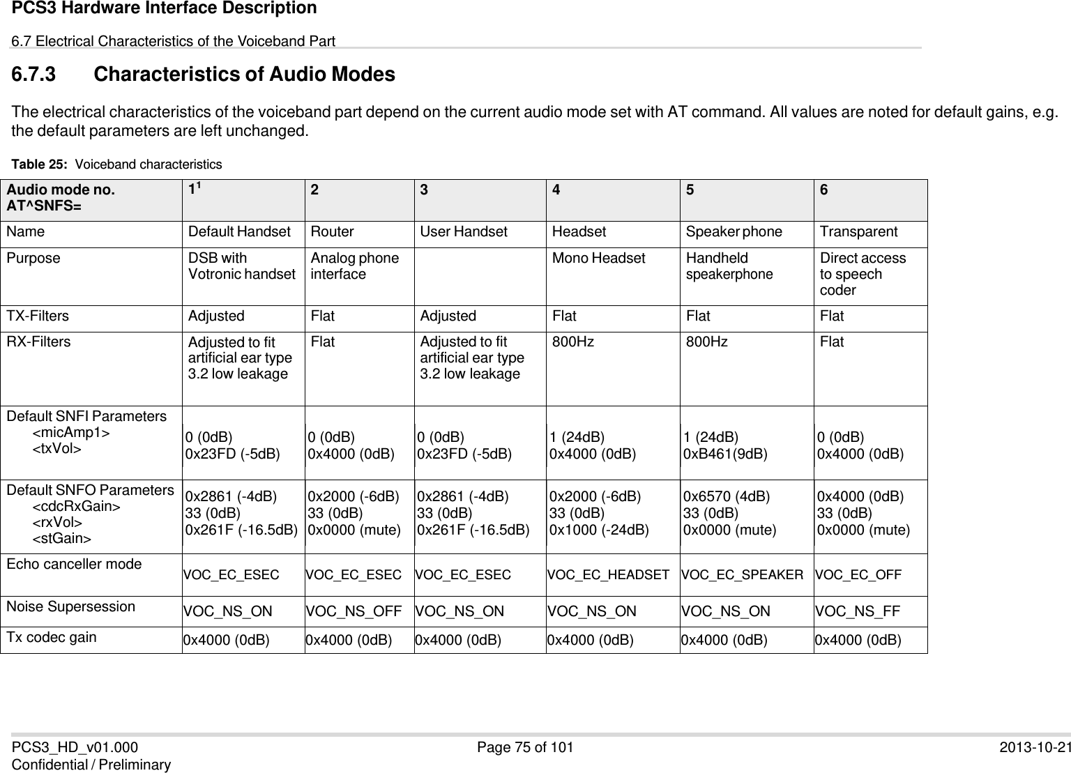
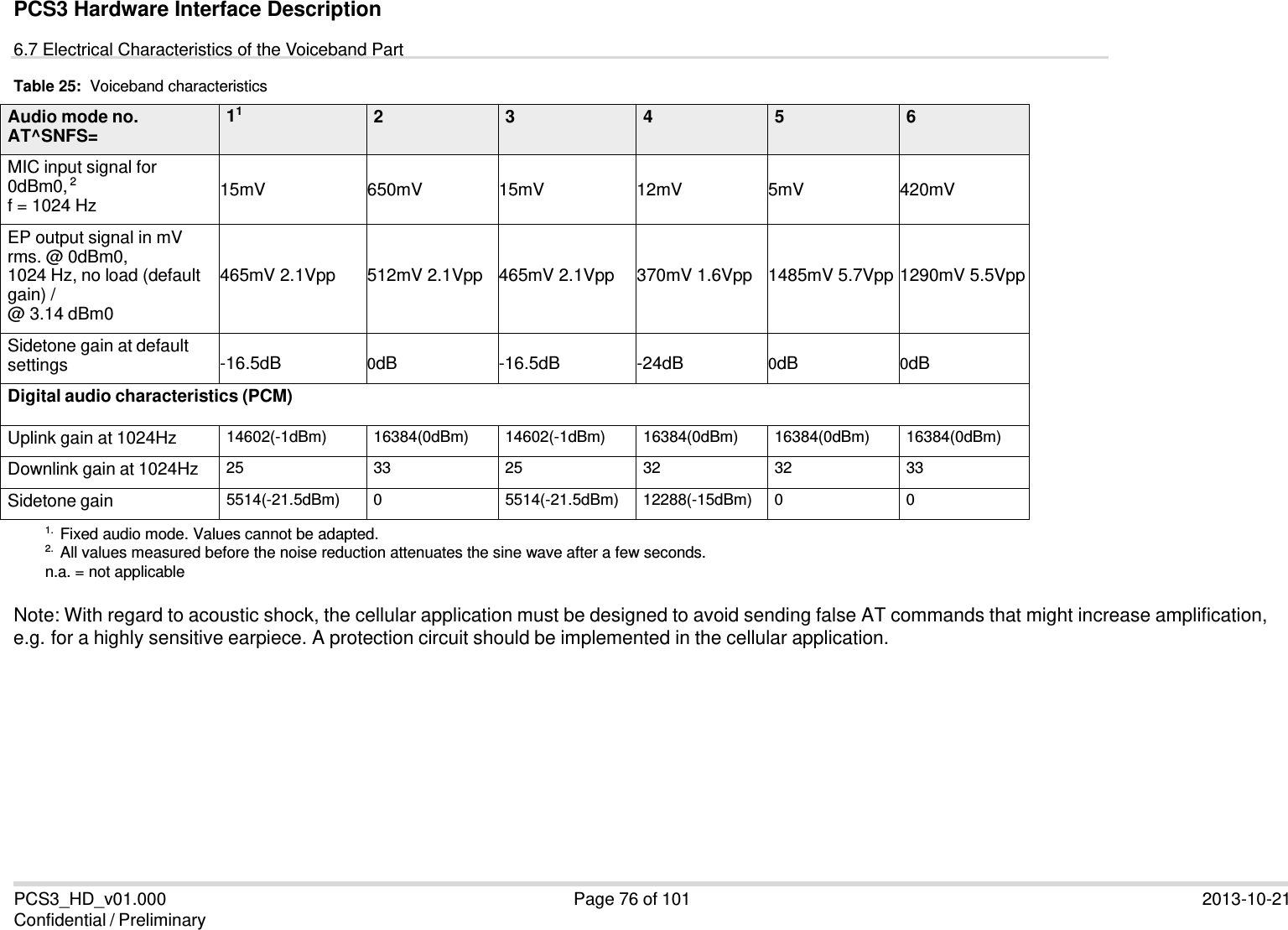
![PCS3_HD_v01.000 Confidential / Preliminary Page 73 of 101 2013-10-21 PCS3 Hardware Interface Description6.7 Electrical Characteristics of the Voiceband Part6.7 Electrical Characteristics of the Voiceband Part 6.7.1 Setting Audio Parameters by AT Commands Audio mode 1 is the basic audio mode optimized for the Votronic reference handset (see Sec- tion 10.1). The default parameters are determined for type approval and are not adjustable with AT commands. The audio modes 2 to 8 can be temporarily adjusted according to the AT command parameters listed in the table below. The audio parameters are set with the AT commands AT^SNFI as well as AT^SNFO and stored volatile for the current audio mode (see [1]). For a model of how the parameters influence the audio signal path see Section 6.7.2. Table 24: Audio parameters adjustable by AT command Parameter Influence to Range Gain range Calculation AT^SNFI= micAmp1 MICP/MICN second analog ampli- fier gain of before ADC 0,1 0 or 24dB micTxVol Digital gain of input signal after ADC 0, 1...65535 Mute, -84...+12dB 20 * log (micTxVol/ 16384) AT^SNFO= cdcRxGain Analog gain of output signal after summation of sidetone 0...63 -57...+6dB 1dB steps rxVol Digital Volume of output signal after speech decoder, before summation of sidetone and DAC 0, 1…41 Mute, -48...+12dB 1.5dB steps stGain Digital attenuation of sidetone 0, 1...65535 Mute, -96...0dB 20 * log (stGain/ 16384) -12](https://usermanual.wiki/THALES-DIS-AlS-Deutschland/PCS3/User-Guide-2113265-Page-67.png)
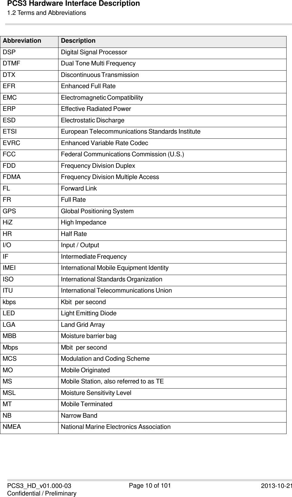
![PCS3_HD_v01.000 Confidential / Preliminary Page 74 of 101 2013-10-21 PCS3 Hardware Interface Description6.7 Electrical Characteristics of the Voiceband PartEcho canceller,Noise suppressonwith one or two Micro- phonesFilter flat gain=0dB 6.7.2 Audio Programming Model The audio programming model shows how the signal path can be influenced by varying AT command parameters: AT^SNFI allows to set the parameters <micAmp1>, and<mic TxVol>, whereas the parameters <cdcRxGain>, <stGain> and <rxVol> can be adjusted with AT^SNFO. For more information on the AT commands and parameters see Section 6.7.1 and [1]. If the digital audio interface (PCM) is selected, the parameters <micAmp1>, and <cdcRxGain> have no influence; because they are not involved in the signal paths.(PCS3 didn’t support I2S) Application Digital logical channels: gain=0dB <io> gain=0dB Aux MIC Main MIC Speaker Codec I2S right channel I2S left channel / PCM mono 4 PCM mono I2S left channel 4 PCM / I2S Interface I2S Interface 1 3 2 <micTxVol> Speech coder VMIC Codec MIC Microphone feeding EP <micAmp1> A D <cdcRxGain> D gain=0dB PCM 1 3 2 <stGain> 3 2 <rxVol> Filter Speech coder 32 Ohms A flat gain=0dB Module Red: Audio mode parameters adjustable by AT commands Orange: Selectable Audio Mode Parameter - on request adjustable by Cinterion Figure 34: Audio programming model](https://usermanual.wiki/THALES-DIS-AlS-Deutschland/PCS3/User-Guide-2113265-Page-68.png)
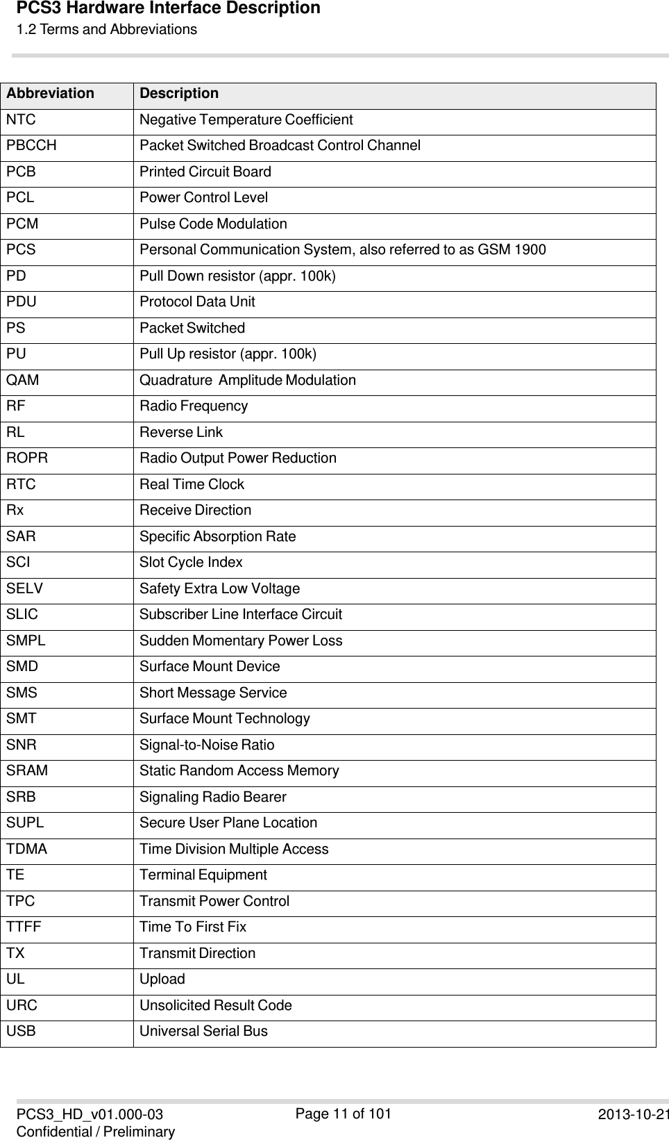
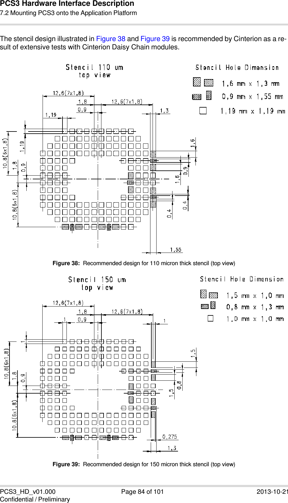
![PCS3 Hardware Interface Description7.2 Mounting PCS3 onto the Application PlatformPCS3_HD_v01.000 Confidential / Preliminary Page 83 of 101 2013-10-217.2 Mounting PCS3 onto the Application Platform This section describes how to mount PCS3 onto the PCBs (=printed circuit boards), including land pattern and stencil design, board-level characterization, soldering conditions, durability and mechanical handling. For more information on issues related to SMT module integration see also [4]. Note: All SMT module pads need to be soldered to the application’s PCB. Not only must all sup- ply pads and signals be connected appropriately, but all pads denoted as “Do not use“ will also have to be soldered (but not electrically connected) in order to ensure the best possible me- chanical stability. 7.2.1 SMT PCB Assembly 7.2.1.1 Land Pattern and Stencil The land pattern and stencil design as shown below is based on Cinterion characterizations for lead-free solder paste on a four-layer test PCB and a 110 respectively 150 micron-thick stencil. The land pattern given in Figure 37 reflects the module‘s pad layout, including signal pads and ground pads (for pad assignment see Section 6.5). Besides these pads there are ground areas on the module's bottom side that must not be soldered, e.g., the position marker. To prevent short circuits, it has to be ensured that there are no wires on the external application side that may connect to these module ground areas. Figure 37: Land pattern (top view)](https://usermanual.wiki/THALES-DIS-AlS-Deutschland/PCS3/User-Guide-2113265-Page-76.png)
![PCS3 Hardware Interface Description7.2 Mounting PCS3 onto the Application PlatformPCS3_HD_v01.000 Confidential / Preliminary Page 85 of 101 2013-10-217.2.1.2 Board Level Characterization Board level characterization issues should also be taken into account if devising an SMT pro- cess. Characterization tests should attempt to optimize the SMT process with regard to board level reliability. This can be done by performing the following physical tests on sample boards: Peel test, bend test, tensile pull test, drop shock test and temperature cycling. Sample surface mount checks are described in [4]. It is recommended to characterize land patterns before an actual PCB production, taking individual processes, materials, equipment, stencil design, and reflow profile into account. For land and stencil pattern design recommendations see also Section 7.2.1.1. Optimizing the solder stencil pattern design and print process is necessary to ensure print uniformity, to decrease sol- der voids, and to increase board level reliability. Daisy chain modules for SMT characterization are available on request. For details refer to [4]. Generally, solder paste manufacturer recommendations for screen printing process parameters and reflow profile conditions should be followed. Maximum ratings are described in Section 7.2.3. 7.2.2 Moisture Sensitivity Level PCS3 comprises components that are susceptible to damage induced by absorbed moisture. Cinterion’s PCS3 module complies with the latest revision of the IPC/JEDEC J-STD-020 standard for moisture sensitive surface mount devices and is classified as MSL 4. For additional MSL (=moisture sensitivity level) related information see Section 7.2.4 and Sec- tion 7.3.2.](https://usermanual.wiki/THALES-DIS-AlS-Deutschland/PCS3/User-Guide-2113265-Page-78.png)
![PCS3_HD_v01.000 Confidential / Preliminary Page 94 of 101 2013-10-21 PCS3 Hardware Interface Description8 Sample Application 8 Sample Application Figure 47 shows a typical example of how to integrate an PCS3 module with an application. The audio interface demonstrates the balanced connection of microphone and earpiece. This solution is particularly well suited for internal transducers. The PWR_IND line is an open collector that needs an external pull-up resistor which connects to the voltage supply VCC µC of the microcontroller. Low state of the open collector pulls the PWR_IND signal low and indicates that the PCS3 module is active, high level notifies the Pow- er-down mode. If the module is in Power-down mode avoid current flowing from any other source into the mod- ule circuit, for example reverse current from high state external control lines. Therefore, the controlling application must be designed to prevent reverse flow. If an external level controller is required, this can be done by using for example a 5V I/O tolerant buffer/driver like a "74AVC4T245" with OE (Output Enable) controlled by PWR_IND. While developing SMT applications it is strongly recommended to provide test points for certain signals resp. lines to and from the module - for debug and/or test purposes. The SMT application should allow for an easy access to these signals. For details on how to implement test points see [4]. The EMC measures are best practice recommendations. In fact, an adequate EMC strategy for an individual application is very much determined by the overall layout and, especially, the po- sition of components. Disclaimer: No warranty, either stated or implied, is provided on the sample schematic diagram shown in Figure 47 and the information detailed in this section. As functionality and compliance with na- tional regulations depend to a great amount on the used electronic components and the indi- vidual application layout manufacturers are required to ensure adequate design and operating safeguards for their products using PCS3 modules.](https://usermanual.wiki/THALES-DIS-AlS-Deutschland/PCS3/User-Guide-2113265-Page-87.png)