THALES DIS AlS Deutschland PCS3 CDMA 1XRTT MODULE User Manual Rev
Gemalto M2M GmbH CDMA 1XRTT MODULE Rev
User Manual Rev

Hardwa
r
e Interface Description
PCS3
Version: 01.000-03
Document: PCS3_HD_v01.000-03

PCS3_HD_v01.000-03
Confidential / Preliminary Page 2 of 101 2013-10-21
PCS3 Hardware Interface Description
Document Name: PCS3 Hardware Interface Description
Version: 01.000-03
Date: 2013-10-21
Document: PCS3_HD_v01.000-03
Status Confidential / Preliminary
GENERAL NOTE
THE USE OF THE PRODUCT INCLUDING THE SOFTWARE AND DOCUMENTATION (THE "PROD-
UCT") IS SUBJECT TO THE RELEASE NOTE PROVIDED TOGETHER WITH PRODUCT. IN ANY
EVENT THE PROVISIONS OF THE RELEASE NOTE SHALL PREVAIL. THIS DOCUMENT CON-
TAINS INFORMATION ON CINTERION PRODUCTS. THE SPECIFICATIONS IN THIS DOCUMENT
ARE SUBJECT TO CHANGE AT CINTERION'S DISCRETION. CINTERION WIRELESS MODULES
GMBH GRANTS A NON-EXCLUSIVE RIGHT TO USE THE PRODUCT. THE RECIPIENT SHALL NOT
TRANSFER, COPY, MODIFY, TRANSLATE, REVERSE ENGINEER, CREATE DERIVATIVE WORKS;
DISASSEMBLE OR DECOMPILE THE PRODUCT OR OTHERWISE USE THE PRODUCT EXCEPT
AS SPECIFICALLY AUTHORIZED. THE PRODUCT AND THIS DOCUMENT ARE PROVIDED ON AN
"AS IS" BASIS ONLY AND MAY CONTAIN DEFICIENCIES OR INADEQUACIES. TO THE MAXIMUM
EXTENT PERMITTED BY APPLICABLE LAW, CINTERION WIRELESS MODULES GMBH DIS-
CLAIMS ALL WARRANTIES AND LIABILITIES. THE RECIPIENT UNDERTAKES FOR AN UNLIMITED
PERIOD OF TIME TO OBSERVE SECRECY REGARDING ANY INFORMATION AND DATA PRO-
VIDED TO HIM IN THE CONTEXT OF THE DELIVERY OF THE PRODUCT. THIS GENERAL NOTE
SHALL BE GOVERNED AND CONSTRUED ACCORDING TO GERMAN LAW.
Copyright
Transmittal, reproduction, dissemination and/or editing of this document as well as utilization of its con-
tents and communication thereof to others without express authorization are prohibited. Offenders will
be held liable for payment of damages. All rights created by patent grant or registration of a utility model
or design patent are reserved.
Copyright © 2013, Cinterion Wireless Modules GmbH
Trademark Notice
Microsoft and Windows are either registered trademarks or trademarks of Microsoft Corporation in the
United States and/or other countries. CDMA2000 is a registered certification mark of the Telecommuni-
cations Industry Association. All other registered trademarks or trademarks mentioned in this document
are property of their respective owners.

PCS3_HD_v01.000-03
Confidential / Preliminary Page 3 of 101 2013-10-21
PCS3 Hardware Interface Description
Contents
Contents
0 Document History ....................................................................................................... 8
1
Introduction
.............................................................................................................. 10
1.1
Related Documents
......................................................................................... 10
1.2
Terms and Abbreviations
................................................................................. 10
1.3
Regulatory and Type Approval Information
..................................................... 13
1.3.1
Directives and Standards
................................................................... 13
1.3.2
SAR requirements specific to portable mobiles
.................................. 15
1.3.3
SELV Requirements
........................................................................... 16
1.3.4
Safety Precautions
............................................................................. 16
2
Product Concept
....................................................................................................... 18
2.1
Key Features at a Glance
................................................................................ 18
2.2
PCS3 System Overview
.................................................................................. 20
2.3
Circuit Concept
................................................................................................ 21
3
Application Interface
................................................................................................ 22
3.1
Operating Modes
............................................................................................. 23
3.2
Power Supply
.................................................................................................. 24
3.2.1
Monitoring Power Supply by AT Command
........................................ 25
3.3
Power-Up / Power-Down Scenarios
................................................................ 26
3.3.1
Turn on PCS3
..................................................................................... 26
3.3.2
Signal States after Startup
.................................................................. 27
3.3.3
Turn off PCS3 Using AT Command
.................................................... 28
3.3.4
Configuring the IGT Line for Use as ON/OFF Switch
......................... 29
3.3.5
Automatic Shutdown
........................................................................... 30
3.3.5.1
Thermal Shutdown
.............................................................. 31
3.3.5.2
Undervoltage Shutdown
...................................................... 32
3.3.5.3
Overvoltage Shutdown
........................................................ 32
3.3.6
Automatic Reset
................................................................................. 32
3.3.7 Turn off PCS3 in Case of Emergency..………………………………....33
3.4
Power Saving
.................................................................................................. 34
3.4.1
Power Saving while Attached to CDMA Networks
.............................. 34
3.4.2
Timing of the CTS0 Signal, CDMA
..................................................... 34
3.4.3
Wake up from or Disabling Power Saving
.......................................... 35
3.5
RTC Backup
.................................................................................................... 36
3.6
USB Interface
.................................................................................................. 37
3.6.1
Reducing Power Consumption
........................................................... 38
3.7
Serial Interface ASC0
...................................................................................... 39
3.8
Analog Audio Interface
.................................................................................... 41
3.8.1
Microphone Inputs and Supply
........................................................... 42
3.8.2
Loudspeaker Output
........................................................................... 45
3.9
Digital Audio Interface
..................................................................................... 46
3.9.1
Pulse Code Modulation Interface (PCM)
............................................ 46

PCS3_HD_v01.000-03
Confidential / Preliminary Page 4 of 101 2013-10-21
PCS3 Hardware Interface Description
Contents
3.9.2
Inter I2C Interface
.............................................................................. 48
3.10
Control Signals ................................................................................................ 50
3.10.1
PWR_IND Signal
................................................................................ 50
3.10.2
Network Connectivity Status Signals
.................................................. 50
3.10.3
Behavior of the RING0 Line (ASC0 Interface only)
............................. 51
3.10.4
Host Wakeup
...................................................................................... 51
3.10.5
Low Current Indicator
......................................................................... 52
3.10.6
RING0 (ASC0), WAKEUP and LCI_IND Startup Behavior
................. 53
4
Antenna Interfaces
................................................................................................... 55
4.1
CDMA Antenna Interface
................................................................................. 55
4.1.1
Antenna Installation
............................................................................ 56
4.1.2
RF Line Routing Design
..................................................................... 57
4.1.2.1
Line Arrangement Examples
............................................... 57
4.1.2.2
Routing Example
................................................................ 59
5
Electrical, Reliability and Radio Characteristics
.................................................... 62
5.1
Absolute Maximum Ratings
............................................................................. 62
5.2
Operating Temperatures
................................................................................. 63
5.3
Storage Conditions
.......................................................................................... 63
5.4
Reliability Characteristics
................................................................................ 64
5.5
Pad Assignment and Signal Description
.......................................................... 64
5.6
Power Supply Ratings
..................................................................................... 72
5.7
Electrical Characteristics of the Voiceband Part
.............................................. 73
5.7.1
Setting Audio Parameters by AT Commands
..................................... 73
5.7.2
Audio Programming Model
................................................................. 74
5.7.3
Characteristics of Audio Modes
.......................................................... 75
5.7.4
Voiceband Receive Path
.................................................................... 77
5.7.5
Voiceband Transmit Path
................................................................... 77
5.8
RF Antenna Interface Characteristics
.............................................................. 78
5.9
Electrostatic Discharge .................................................................................... 79
6
Mechanics, Mounting and Packaging
..................................................................... 81
6.1
Mechanical Dimensions of PCS3
.................................................................... 81
6.2
Mounting PCS3 onto the Application Platform
................................................. 83
6.2.1
SMT PCB Assembly
........................................................................... 83
6.2.1.1
Land Pattern and Stencil
..................................................... 83
6.2.1.2
Board Level Characterization
.............................................. 85
6.2.2
Moisture Sensitivity Level
................................................................... 85
6.2.3
Soldering Conditions and Temperature
.............................................. 86
6.2.3.1
Reflow Profile
..................................................................... 86
6.2.3.2
Maximum Temperature and Duration
.................................. 87
6.3
Durability and Mechanical Handling
................................................... 88
6.3.1.1
Storage Life
........................................................................ 88
6.3.1.2
Processing Life
................................................................... 88

PCS3_HD_v01.000-03
Confidential / Preliminary Page 5 of 101 2013-10-21
PCS3 Hardware Interface Description
Contents
6.3.1.3
Baking
................................................................................ 88
6.3.1.4
Electrostatic Discharge
....................................................... 88
6.4
Packaging
....................................................................................................... 89
6.4.1
Tape and Reel
.................................................................................... 89
6.4.1.1
Orientation
.......................................................................... 89
6.4.1.2
Barcode Label
..................................................................... 90
6.4.2
Shipping Materials
.............................................................................. 91
6.4.2.1
Moisture Barrier Bag
........................................................... 91
6.4.2.2
Transportation Box
.............................................................. 93
7
Sample Application
.................................................................................................. 94
8
Reference Approval
.................................................................................................. 96
8.1
Reference Equipment for Type Approval
......................................................... 96
8.2
Compliance with FCC and IC Rules and Regulations
..................................... 97
9
Appendix
................................................................................................................... 98
9.1
List of Parts and Accessories
.......................................................................... 98
9.2
Mounting Advice Sheet
.................................................................................. 100

PCS3_HD_v01.000-03
Confidential / Preliminary Page 6 of 101 2013-10-21
PCS3 Hardware Interface Description
Tables
Tables
Table 1: Directives ........................................................................................................ 13
Table 2: Standards of North American type approval ................................................... 13
Table 3: Requirements of quality................................................................................... 13
Table 4: Standards of the Ministry of Information Industry of the
People’s Republic of China ............................................................................. 14
Table 5: Toxic or hazardous substances or elements with defined concentration
limits ................................................................................................................ 14
Table 6: Overview of operating modes.......................................................................... 23
Table 7: Signal states. ................................................................................................... 27
Table 8: Temperature dependent behavior ................................................................... 31
Table 9: DCE-DTE wiring of ASC0 ................................................................................ 40
Table 10: Feedback resistor values versus input gain .................................................... 43
Table 11: Configuration combinations for the PCM interface .......................................... 46
Table 12: Overview of PCM signal functions ................................................................... 46
Table 13: Overview of I2C signal functions ...................................................................... 48
Table 14: Host wakeup lines ........................................................................................... 51
Table 15: Low current indicator line ................................................................................ 52
Table 16: Return loss in the active band ......................................................................... 55
Table 17: Absolute maximum ratings .............................................................................. 62
Table 18: Board temperature .......................................................................................... 63
Table 19: Storage conditions ........................................................................................... 63
Table 20: Summary of reliability test conditions .............................................................. 64
Table 21: Overview: Pad assignments ............................................................................ 65
Table 22: Signal description ............................................................................................ 68
Table 23: Power supply ratings ....................................................................................... 72
Table 24: Audio parameters adjustable by AT command ............................................... 73
Table 25: Voiceband characteristics ............................................................................... 75
Table 26: Voiceband receive path. .................................................................................. 77
Table 27: Voiceband transmit path.................................................................................. 77
Table 28: RF Antenna interface CDMA. .......................................................................... 78
Table 29: Electrostatic values ......................................................................................... 80
Table 30: Reflow temperature ratings ............................................................................. 87
Table 31: List of parts and accessories. .......................................................................... 98
Table 32: Molex sales contacts (subject to change) ....................................................... 99
Table 33: Hirose sales contacts (subject to change) ....................................................... 99

PCS3_HD_v01.000-03
Confidential / Preliminary Page 7 of 101 2013-10-21
PCS3 Hardware Interface Description
Figures
Figures
Figure 1: PCS3 system overview
.................................................................................. 20
Figure 2: PCS3 block diagram
....................................................................................... 21
Figure 3: Decoupling capacitor(s) for BATT+
................................................................. 24
Figure 4: Power-on with IGT
.......................................................................................... 26
Figure 5: Signal states during turn-off procedure
........................................................... 28
Figure 6: Timing of IGT if used as ON/OFF switch
........................................................ 29
Figure 7: Shutdown by EMERG_OFF signal
................................................................. 33
Figure 8: RTC supply variants
....................................................................................... 36
Figure 9: USB circuit
...................................................................................................... 37
Figure 10: Serial interface ASC0
..................................................................................... 39
Figure 11: Structure of Audio Input and Supply
............................................................... 42
Figure 12: Single ended microphone connection
............................................................. 44
Figure 13: Differential microphone connection
................................................................ 44
Figure 14: Line input
........................................................................................................ 45
Figure 15: Differential loudspeaker connection
................................................................ 45
Figure 16: Line output connection
................................................................................... 45
Figure 17: PCM timing short frame (master/slave, 256, 512 or 2048KHz)
....................... 47
Figure 18: PCM timing long frame (master, 128kHz)
....................................................... 47
Figure 19: I2C interface timing
......................................................................................... 49
Figure 20: Dual microphone design example with I2S interface
....................................... 49
Figure 21: PWR_IND signal
............................................................................................. 50
Figure 22: LED Circuit (Example).
................................................................................... 50
Figure 23: Low current indication timing
.......................................................................... 52
Figure 24: RING0 (ASC0), WAKEUP and LCI_IND startup behavior
.............................. 53
Figure 25: Antenna pads
................................................................................................. 56
Figure 26: Coated coplanar strip with ground
.................................................................. 57
Figure 27: Differnetia coated coplanar strip with ground
................................................. 58
Figure 28: Routing to application‘s RF connector
............................................................ 59
Figure 29: PCS3 evaluation board layer table
................................................................. 59
Figure 30: PCS3 bottom view: Pad assignments
............................................................. 66
Figure 31: Audio programming model
............................................................................. 74
Figure 32: PCS3 – top and bottomview
........................................................................... 81
Figure 33: Dimensions of PCS3 (all dimensions in mm)
.................................................. 82
Figure 34: Land pattern (top view)
................................................................................... 83
Figure 35: Recommended design for 110 micron thick stencil (top view)
........................ 84
Figure 36: Recommended design for 150 micron thick stencil (top view)
........................ 84
Figure 37: Reflow Profile
................................................................................................. 86
Figure 38: Carrier tape
.................................................................................................... 89
Figure 39: Roll direction
................................................................................................... 89
Figure 40: Barcode label on tape reel
.............................................................................. 90
Figure 41: Moisture barrier bag (MBB) with imprint
......................................................... 91
Figure 42: Moisture Sensitivity Label
............................................................................... 92
Figure 43: Humidity Indicator Card - HIC
......................................................................... 93
Figure 44: PCS3 sample application
............................................................................... 95
Figure 45: Reference equipment for type approval
.......................................................... 96

PCS3_HD_v01.000-03
Confidential / Preliminary Page 8 of 101 2013-10-21
PVS8 Hardware Interface Description
0 Document History
PVS8 Hardware Interface Description
0 Document History
PVS8 Hardware Interface Description
0 Document History
0 Document History
New document: "PCS3 Hardware Interface Description" Version 01.000-03
Chapter What is new
-- Initial document release

PCS3_HD_v01.000-03
Confidential / Preliminary Page 9 of 101 2013-10-21
PCS3 Hardware Interface Description
1 Introduction
1
Introduction
The document1 describes the hardware of the PCS3 module, designed to connect to a cellular
device application and the air interface. It helps you quickly retrieve interface specifications,
electrical and mechanical details and information on the requirements to be considered for in-
tegrating further components.
1.1
Related Documents
[1] PCS3 AT Command Set
[2] PCS3 Release Notes
[3] DSB75 Support Box - Evaluation Kit for Cinterion Wireless Modules
[4] Application Note 48: SMT Module Integration
[5] Universal Serial Bus Specification Revision 2.0, April 27, 2000
1.2
Terms and Abbreviations
Abbreviation Description
ANSI American National Standards Institute
AMR Adaptive Multi-rate
ARP Antenna Reference Point
BB Baseband
BC Band Class
BEP Bit Error Probability
BTS Base Transceiver Station
CB or CBM Cell Broadcast Message
CDMA Code Division Multiple Access
CE Conformité Européene (European Conformity)
CS Coding Scheme
CS Circuit Switched
CSD Circuit Switched Data
CTM Cellular Text Modem
DAC Digital-to-Analog Converter
DCS Digital Cellular System
DL Download
DRX Discontinuous Reception
DSB Development Support Board
1.
The document is effective only if listed in the appropriate Release Notes as part of the technical
documentation delivered with your Cinterion Wireless Modules product.

PCS3_HD_v01.000-03
Confidential / Preliminary Page 10 of 101 2013-10-21
PCS3 Hardware Interface Description
1.2 Terms and Abbreviations
Abbreviation Description
DSP Digital Signal Processor
DTMF Dual Tone Multi Frequency
DTX Discontinuous Transmission
EFR Enhanced Full Rate
EMC Electromagnetic Compatibility
ERP Effective Radiated Power
ESD Electrostatic Discharge
ETSI European Telecommunications Standards Institute
EVRC Enhanced Variable Rate Codec
FCC Federal Communications Commission (U.S.)
FDD Frequency Division Duplex
FDMA Frequency Division Multiple Access
FL Forward Link
FR Full Rate
GPS Global Positioning System
HiZ High Impedance
HR Half Rate
I/O Input / Output
IF Intermediate Frequency
IMEI International Mobile Equipment Identity
ISO International Standards Organization
ITU International Telecommunications Union
kbps Kbit per second
LED Light Emitting Diode
LGA Land Grid Array
MBB Moisture barrier bag
Mbps Mbit per second
MCS Modulation and Coding Scheme
MO Mobile Originated
MS Mobile Station, also referred to as TE
MSL Moisture Sensitivity Level
MT Mobile Terminated
NB Narrow Band
NMEA National Marine Electronics Association

PCS3_HD_v01.000-03
Confidential / Preliminary Page 11 of 101 2013-10-21
PCS3 Hardware Interface Description
1.2 Terms and Abbreviations
Abbreviation Description
NTC Negative Temperature Coefficient
PBCCH Packet Switched Broadcast Control Channel
PCB Printed Circuit Board
PCL Power Control Level
PCM Pulse Code Modulation
PCS Personal Communication System, also referred to as GSM 1900
PD Pull Down resistor (appr. 100k)
PDU Protocol Data Unit
PS Packet Switched
PU Pull Up resistor (appr. 100k)
QAM Quadrature Amplitude Modulation
RF Radio Frequency
RL Reverse Link
ROPR Radio Output Power Reduction
RTC Real Time Clock
Rx Receive Direction
SAR Specific Absorption Rate
SCI Slot Cycle Index
SELV Safety Extra Low Voltage
SLIC Subscriber Line Interface Circuit
SMPL Sudden Momentary Power Loss
SMD Surface Mount Device
SMS Short Message Service
SMT Surface Mount Technology
SNR Signal-to-Noise Ratio
SRAM Static Random Access Memory
SRB Signaling Radio Bearer
SUPL Secure User Plane Location
TDMA Time Division Multiple Access
TE Terminal Equipment
TPC Transmit Power Control
TTFF Time To First Fix
TX Transmit Direction
UL Upload
URC Unsolicited Result Code
USB Universal Serial Bus

PCS3_HD_v01.000-03
Confidential / Preliminary Page 12 of 101 2013-10-21
PCS3 Hardware Interface Description
1.3 Regulatory and Type Approval Information
1.3
Regulatory and Type Approval Information
1.3.1
Directives and Standards
PCS3 has been designed to comply with the directives and standards listed below.
It is the responsibility of the application manufacturer to ensure compliance of the final product
with all provisions of the applicable directives and standards as well as with the technical spec-
ifications provided in the "PCS3 Hardware Interface Description".1
Table 1: Directives
2002/95/EC Directive of the European Parliament and of the Council of
27 January 2003 on the restriction of the use of certain haz-
ardous substances in electrical and electronic equipment
(RoHS)
Table 2: Standards of North American type approval
CFR Title 47 Code of Federal Regulations, Part 22, Part 24 and Part 27; US Equipment
Authorization FCC
OET Bulletin 65
(Edition 97-01) Evaluating Compliance with FCC Guidelines for Human Exposure to Radio-
frequency Electromagnetic Fields
UL 60 950-1 Product Safety Certification (Safety requirements)
NAPRD.03 V5.11 Overview of PCS Type certification review board Mobile Equipment Type
Certification and IMEI control
PCS Type Certification Review board (PTCRB)
RSS132, RSS133,
RSS139 Canadian Standard
Table 3: Requirements of quality
IEC 60068 Environmental testing
DIN EN 60529 IP codes
1.
Manufacturers of applications which can be used in the US shall ensure that their applications have a
PTCRB approval. For this purpose they can refer to the PTCRB approval of the respective module.
PCS3_HD_v01.000-03
Confidential / Preliminary Page 13 of 101 2013-10-21
PCS3 Hardware Interface Description
1.3 Regulatory and Type Approval Information
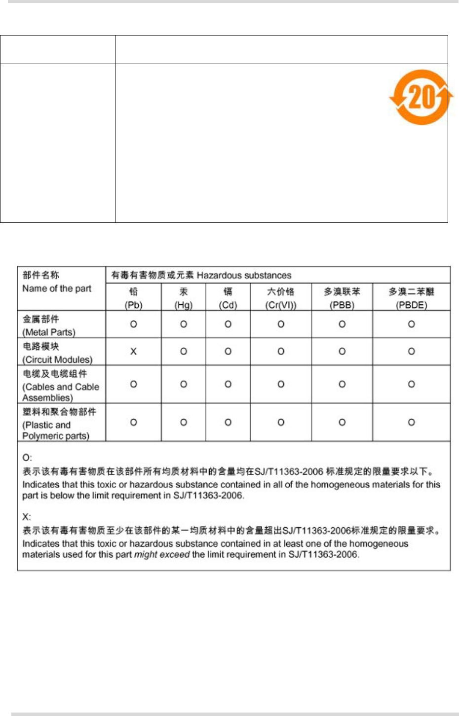
Table 4: Standards of the Ministry of Information Industry of the People’s Republic of China
SJ/T 11363-2006 “Requirements for Concentration Limits for Certain Hazardous Substances
in Electronic Information Products” (2006-06).
SJ/T 11364-2006 “Marking for Control of Pollution Caused by Electronic
Information Products” (2006-06).
According to the “Chinese Administration on the Control of
Pollution caused by Electronic Information Products”
(ACPEIP) the EPUP, i.e., Environmental Protection Use
Period, of this product is 20 years as per the symbol
shown here, unless otherwise marked. The EPUP is valid only as long as
the product is operated within the operating limits described in the Cinterion
Hardware Interface Description.
Please see Table 5 for an overview of toxic or hazardous substances or ele-
ments that might be contained in product parts in concentrations above the
limits defined by SJ/T 11363-2006.
Table 5: Toxic or hazardous substances or elements with defined concentration limits

PCS3_HD_v01.000-03
Confidential / Preliminary Page 14 of 101 2013-10-21
PCS3 Hardware Interface Description
1.3 Regulatory and Type Approval Information
1.3.2
SAR requirements specific to portable mobiles
Mobile phones, PDAs or other portable transmitters and receivers incorporating a CDMA mod-
ule must be in accordance with the guidelines for human exposure to radio frequency energy.
This requires the Specific Absorption Rate (SAR) of portable PCS3 based applications to be
evaluated and approved for compliance with national and/or international regulations.
Since the SAR value varies significantly with the individual product design manufacturers are
advised to submit their product for approval if designed for portable use. For US markets the
relevant directives are mentioned below. It is the responsibility of the manufacturer of the final
product to verify whether or not further standards, recommendations or directives are in force
outside these areas.
Products intended for sale on US markets
ES 59005/ANSI C95.1 Considerations for evaluation of human exposure to electromagnetic
fields (EMFs) from mobile telecommunication equipment (MTE) in the
frequency range 30MHz - 6GHz
IMPORTANT:
Manufacturers of portable applications based on PCS3 modules are required to have their final
product certified and apply for their own FCC Grant and Industry Canada Certificate related to
the specific portable mobile.
PCS3_HD_v01.000-03
Confidential / Preliminary Page 15 of 101 2013-10-21
PCS3 Hardware Interface Description
1.3 Regulatory and Type Approval Information
1.3.3
SELV Requirements
The power supply connected to the PCS3 module shall be in compliance with the SELV re-
quirements defined in EN 60950-1.
1.3.4
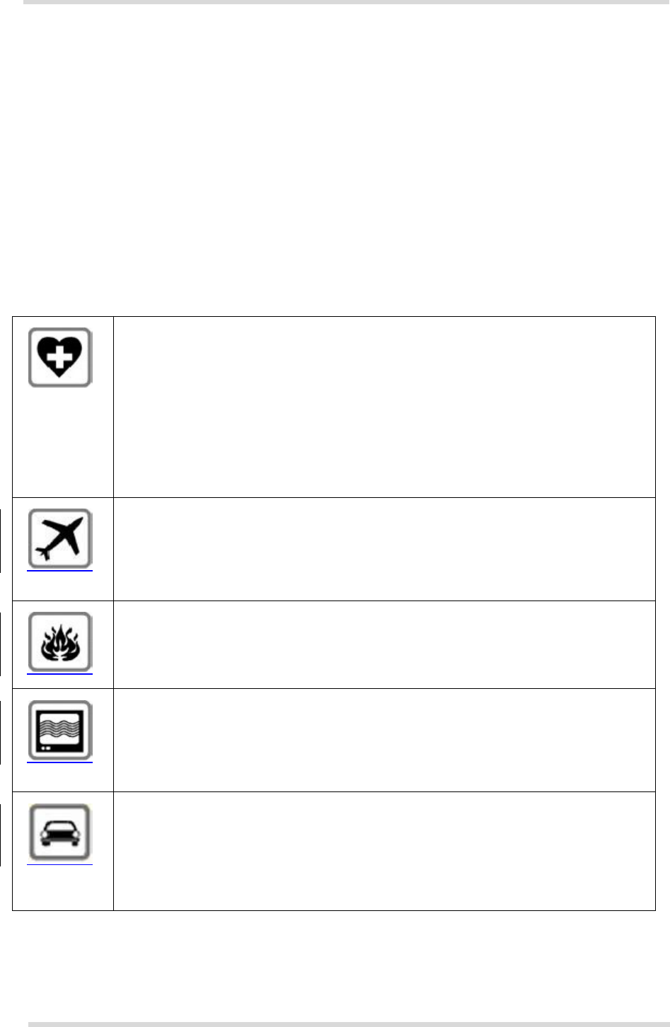
Safety Precautions
The following safety precautions must be observed during all phases of the operation, usage,
service or repair of any cellular terminal or mobile incorporating PCS3. Manufacturers of the
cellular terminal are advised to convey the following safety information to users and operating
personnel and to incorporate these guidelines into all manuals supplied with the product. Fail-
ure to comply with these precautions violates safety standards of design, manufacture and in-
tended use of the product. Cinterion Wireless Modules assumes no liability for customer’s
failure to comply with these precautions.
When in a hospital or other health care facility, observe the restrictions on the use of
mobiles. Switch the cellular terminal or mobile off, if instructed to do so by the guide-
lines posted in sensitive areas. Medical equipment may be sensitive to RF energy.
The operation of cardiac pacemakers, other implanted medical equipment and hearing
aids can be affected by interference from cellular terminals or mobiles placed close to
the device. If in doubt about potential danger, contact the physician or the manufac-
ture of the device to verify that the equipment is properly shielded. Pacemaker
patients are advised to keep their hand-held mobile away from the pacemaker, while
it is on.
Switch off the cellular terminal or mobile before boarding an aircraft. Make sure it can-
not be switched on inadvertently. The operation of wireless appliances in an aircraft is
forbidden to prevent interference with communications systems. Failure to observe
these instructions may lead to the suspension or denial of cellular services to the
offender, legal action, or both.
Do not operate the cellular terminal or mobile in the presence of flammable gases or
fumes. Switch off the cellular terminal when you are near petrol stations, fuel depots,
chemical plants or where blasting operations are in progress. Operation of any electri-
cal equipment in potentially explosive atmospheres can constitute a safety hazard.
Your cellular terminal or mobile receives and transmits radio frequency energy while
switched on. Remember that interference can occur if it is used close to TV sets,
radios, computers or inadequately shielded equipment. Follow any special regulations
and always switch off the cellular terminal or mobile wherever forbidden, or when you
suspect that it may cause interference or danger.
Road safety comes first! Do not use a hand-held cellular terminal or mobile when driv-
ing a vehicle, unless it is securely mounted in a holder for speakerphone operation.
Before making a call with a hand-held terminal or mobile, park the vehicle.
Speakerphones must be installed by qualified personnel. Faulty installation or opera-
tion can constitute a safety hazard.

PCS3_HD_v01.000-03
Confidential / Preliminary Page 16 of 101 2013-10-21
PCS3 Hardware Interface Description
1.3 Regulatory and Type Approval Information
IMPORTANT!
Cellular terminals or mobiles operate using radio signals and cellular networks.
Because of this, connection cannot be guaranteed at all times under all conditions.
Therefore, you should never rely solely upon any wireless device for essential com-
munications, for example emergency calls.
Remember, in order to make or receive calls, the cellular terminal or mobile must be
switched on and in a service area with adequate cellular signal strength.
Some networks do not allow for emergency calls if certain network services or phone
features are in use (e.g. lock functions, fixed dialing etc.). You may need to deactivate
those features before you can make an emergency call.
Bear in mind that exposure to excessive levels of noise can cause physical damage
to users! With regard to acoustic shock, the cellular application must be designed to
avoid unintentional increase of amplification, e.g. for a highly sensitive earpiece. A pro-
tection circuit should be implemented in the cellular application.

PCS3_HD_v01.000-03
Confidential / Preliminary Page 17 of 101 2013-10-21
PCS3 Hardware Interface Description
2 Product Concept
2
Product Concept
2.1
Key Features at a Glance
Feature Implementation
General
Frequency bands CDMA: Dual band (BC0/BC1/BC10), 800/1900MHz
Power supply 3.3V < VBATT+ < 4.2V
Operating temperature
(board temperature) Normal operation: -30°C to +85°C
Restricted operation: -40°C to +95°C
Physical Dimensions: 33mm x 29mm x 2mm
Weight: approx. 4g
RoHS All hardware components fully compliant with EU RoHS Directive
CDMA features
3GPP2 CDMA2000 1xRTT
A
dvanced data rates:
FL max. 307.2kbps, RL max. 307.2kbps
SMS Point-to-point MT and MO
Cell broadcast
Text and PDU mode
General Power saving modes
Software
AT commands Hayes, 3GPP TS 27.007 and 27.005, and proprietary Cinterion Wireless
Modules commands as well as provider specific CDMA commands
Audio Audio speech codecs
3GPP2: EVRC, EVRC-B (4GV-NB), QCELP, AMR-NB
Speakerphone operation, echo cancellation, noise suppression, 6 ringing
tones, TTY support
Software update Generic firmware update from host application over ASC0 or USB

PCS3_HD_v01.000-03
Confidential / Preliminary Page 18 of 101 2013-10-21
PCS3 Hardware Interface Description
2.1 Key Features at a Glance
Feature Implementation
Interfaces
Module interface Surface mount device with solderable connection pads (SMT application
interface).
Land grid array (LGA) technology ensures high solder joint reliability and
provides the possibility to use an optional module mounting socket.
For more information on how to integrate SMT modules see also [4]. This
application note comprises chapters on module mounting and application
layout issues as well as on additional SMT application development
equipment.
Antenna 50Ohms. CDMA main antenna
USB USB 2.0 Full Speed (12Mbit/s)
device interface
Serial interface ASC0:
•
8-wire modem interface with status and control lines, unbalanced,
asynchronous
•
Adjustable baud rates from 1,200bps up to 921,600bps
•
Supports RTS0/CTS0 hardware flow control
Status Signal line to indicate network connectivity state
Audio 1 analog interface with microphone feeding
1 digital interface: PCM
Power on/off, Reset
Power on/off Switch-on by hardware signal IGT
Switch-off by AT command (AT^SMSO)
Automatic switch-off in case of critical temperature or voltage conditions
Reset Orderly shutdown and reset by AT command
Emergency-off Emergency-off by hardware signal EMERG_OFF if IGT is not active
Special Features
Phonebook Phone
TTY/CTM support TTY only
Antenna SAIC (Single Antenna Interference Cancellation) / DARP (Downlink
Advanced Receiver Performance)
Rx diversity (receiver type 3i - 16-QAM)
Over-the-air provisioning Verizon specific OTASP (Over-the-Air Service Provisioning) and OTAPA
(Over-the-Air Parameter Administration)
Evaluation kit
Evaluation module PCS3 module soldered onto a dedicated PCB that can be connected to
an adapter in order to be mounted onto the DSB75.
DSB75 DSB75 Development Support Board designed to test and type approve
Cinterion Wireless Modules and provide a sample configuration for appli-
cation engineering. A special adapter is required to connect the PCS3
evaluation module to the DSB75.
PCS3_HD_v01.000-03
Confidential / Preliminary Page 19 of 101 2013-10-21
PCS3 Hardware Interface Description
2.2 PCS3 System Overview
Modem Interface
Host Wakeup
Power for Application
(VEXT)
Power Indication
(PWR_IND)
Low current
indication
2.2
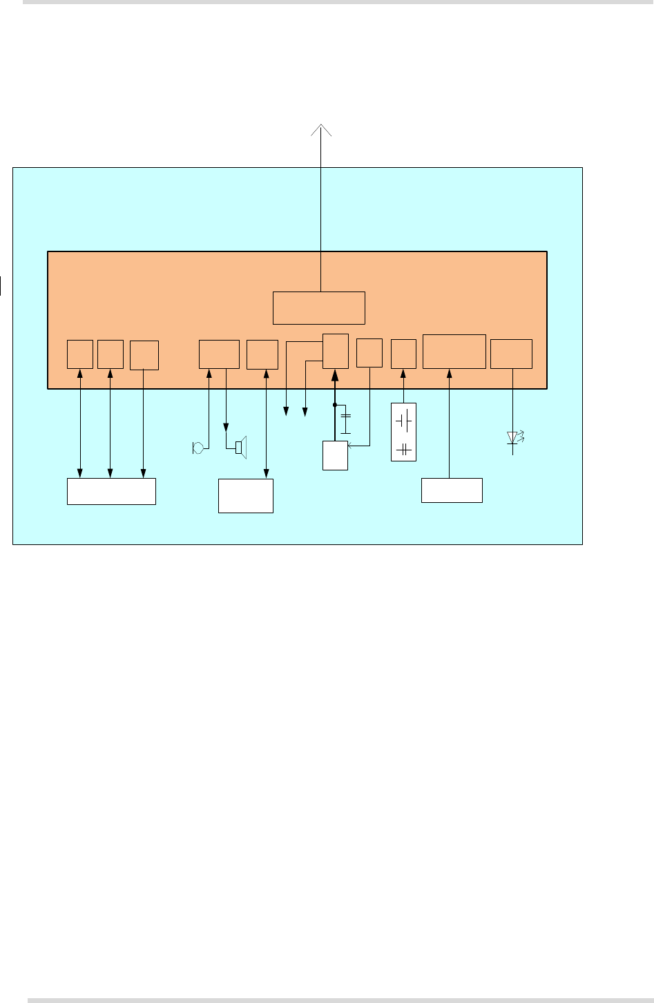
PCS3 System Overview
Application
CDMA Module
USB Serial
ASC0
Wake-
up
Analog
audio
Digital
audio
Power
supply
LCI
IGT,
RTC Emergency Off
Net state/
status
or
PSU
Host Application
Controller
PCM or I2C
Codec
Application
On/Off
Figure 1: PCS3 system overview
CDMAMain
Antenna
PCS3_HD_v01.000-03
Confidential / Preliminary Page 20 of 101 2013-10-21
PCS3 Hardware Interface Description
2.2 PCS3 System Overview
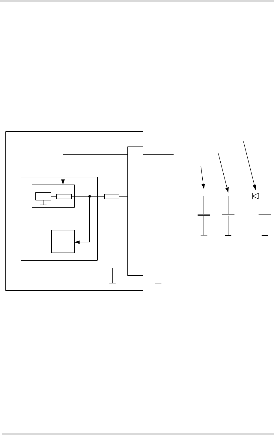
2.3
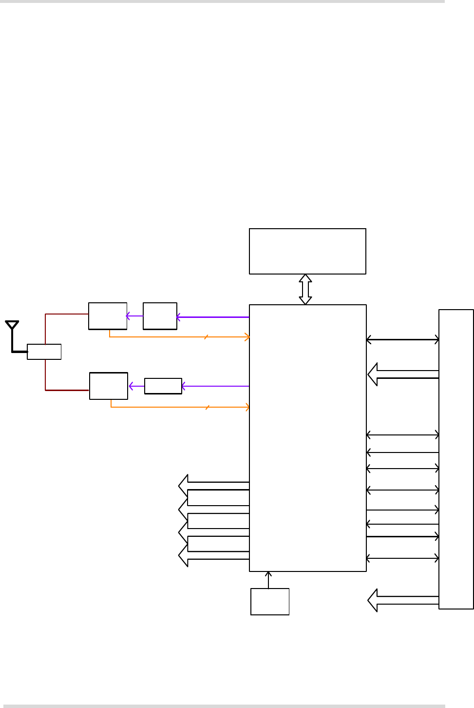
Circuit Concept
Figure 2 shows a block diagram of the PCS3 module and illustrates the major functional com-
ponents:
Baseband block:
•
CDMA controller/transceiver/power supply
•
NOR Flash/pSRAM memory with multiplexed address data bus
•
Audio codec
•
Application interface (SMT with connecting pads)
RF section:
•
RF transceiver
•
RF power amplifier/frontend
•
RF filter
•
Antenna pad
Figure 2: PCS3 block diagram
Interface
(USB, UART, I2C, CSIM)
156 pad
LGA
BATT+
BATT+_CDMA
BC1 PA
PRX_MB2
TX_MB1
Diplexer
BC1
Duplexer
64Mb pSRAM
128Mb NOR flash memory
MCP Memory
EBI1
QSC1105
JTAG
BC0, BC10
PA
BC0, BC10
Duplexer
PRX_LB1
TX_LB1
GPIO
CDMA2000 BC0, BC10
BC0, BC10 TX: 817-849 MHz
BC0, BC10 RX: 862-894 MHz
CDMA2000 BC1
TX: 1850-1910 MHz
RX: 1930-1990 MHz
Analog Audio Interface
(MICP, MICN, EPP, EPN)
ADCx_in
Digital Audio Interface
VEXT
IGT, EMERG_OFF
PWR_IND, STATUS
To PA
To QSC1105 Digtal Core
To QSC1105 RX ADC, RF1
To Memory, QSC1105 digital P1, VEXT,
To QSC1105 digital P4
19.2MHz
Xtal
2.85V
1.8V
2.2V
1.3V
To QSC1105 RF2
To QSC1105 TX, RX ADC
To QSC1105 digital P3
2
2

PCS3_HD_v01.000-03
Confidential / Preliminary Page 21 of 101 2013-10-21
PCS3 Hardware Interface Description
3 Application Interface
3
Application Interface
PCS3 is equipped with an SMT application interface that connects to the external application.
The host interface incorporates several sub-interfaces described in the following sections:
•
Operating modes - see Section 3.1
•
Power supply - see Section 3.2
•
RTC backup - see Section 3.5
•
Serial interface USB - see Section 3.6
•
Serial interface ASC0 - Section 3.7
•
Analog audio interface - see Section 3.8
•
Digital audio interface (PCM) - see Section 3.9
•
Status and control lines: IGT, EMERG_OFF, PWR_IND, STATUS - see Table 22

PCS3_HD_v01.000-03
Confidential / Preliminary Page 22 of 101 2013-10-21
PCS3 Hardware Interface Description
3.1 Operating Modes
3.1
Operating Modes
The table below briefly summarizes the various operating modes referred to in the following
chapters.
Table 6: Overview of operating modes
Mode Function
Normal
operation CDMA SLEEP Power saving set automatically when no call is in progress and the USB
connection is suspended by host or not present and no active commu-
nication via ASC0.
CDMA IDLE Power saving disabled (see [1]: AT^SCFG "MEopMode/
PwrSave",<PwrSaveMode>) or an USB connection not suspended, but
no call in progress.
CDMA TALK/
CDMA DATA CDMA data transfer in progress. Power consumption depends on net-
work settings and data transfer rate.
Power
Down Normal shutdown after sending the AT^SMSO command. Only a voltage regulator is active
for powering the RTC. Software is not active. Interfaces are not accessible. Operating volt-
age (connected to BATT+) remains applied.
Airplane
mode Airplane mode shuts down the radio part of the module, causes the module to log off from
the CDMA network and disables all AT commands whose execution requires a radio con-
nection.
Airplane mode can be controlled by AT command (see [1]).
PCS3_HD_v01.000-03
Confidential / Preliminary Page 23 of 101 2013-10-21
PCS3 Hardware Interface Description
3.2 Power Supply
3.2
Power Supply
PCS3 needs to be connected to a power supply at the SMT application interface - 6 lines each
BATT+ and GND. There are three separate voltage domains for BATT+:
•
BATT+_CDMA with 2 lines for the first power amplifier supply
•
BATT+_CDMA with 2 lines for the second power amplifier supply
•
BATT+ with 2 lines for the general power management.
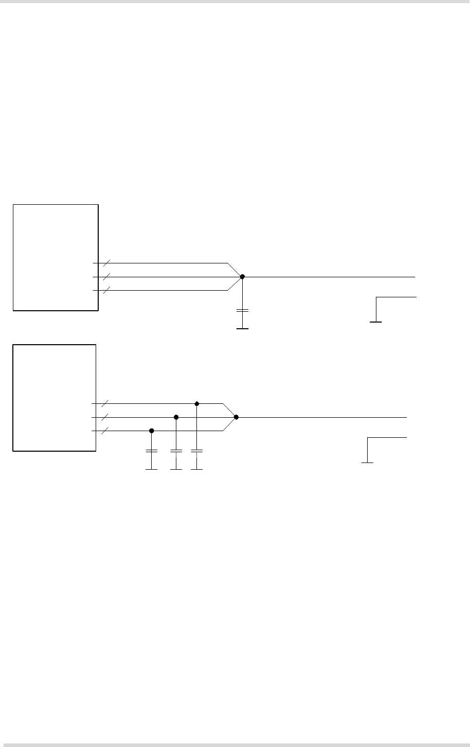
The main power supply from an external application has to be a single voltage source and has
to be expanded to three sub paths (star structure). Capacitors should be placed as close as
possible to the BATT+ pads. Figure 3 shows two sample circuits (minimum requirement and
recommended alternative) for decoupling capacitors for BATT+.
Module
SMT interface
BATT+
BATT+_CDMA
BATT+_CDMA
2
2
2 Decoupling capacitor
BATT+
GND
Minimum requirement
+
e.g. 100…220µF
Ultra-low ESR
Module
SMT interface
BATT+ 2
BATT+_CDMA 2
BATT+_CDMA
2
Recommended alternative
3x
Decoupling capacitors
e.g. 47µF X5R MLCC
BATT+
GND
Figure 3: Decoupling capacitor(s) for BATT+
In addition, the VDDLP signal on the SMT application interface may be connected to an exter-
nal capacitor or a battery to backup the RTC (see Section 3.5).
The power supply of PCS3 must be able to provide the peak current during the uplink transmis-
sion.
All key functions for supplying power to the device are handled by the power management IC.
It provides the following features:
•
Stabilizes the supply voltages for the baseband using switching regulators and low drop lin-
ear voltage regulators.
•
Switches the module's power voltages for the power-up and -down procedures.
•
Delivers, across the VEXT line, a regulated voltage for an external application. This voltage
is not available in Power-down mode and can be reduced via AT command to save power
(see Table 22: VEXT).

PCS3_HD_v01.000-03
Confidential / Preliminary Page 24 of 101 2013-10-21
PCS3 Hardware Interface Description
3.2 Power Supply
3.2.1 Monitoring Power Supply by AT Command
To monitor the supply voltage you can use the AT^SBV command which returns the averaged
value related to BATT+ and GND at the SMT application interface.
The module continuously measures the voltage at intervals depending on the operating mode
of the RF interface. The duration of measuring ranges from 0.5s in TALK/DATA mode to 50s
when PCS3 is in Limited Service (deregistered). The displayed voltage (in mV) is averaged
over the last measuring period before the AT^SBV command was executed.
PCS3_HD_v01.000-03
Confidential / Preliminary Page 25 of 101 2013-10-21
PCS3 Hardware Interface Description
3.3 Power-Up / Power-Down Scenarios
3.3
Power-Up / Power-Down Scenarios
In general, be sure not to turn on PCS3 while it is beyond the safety limits of voltage and tem-
perature stated in Section 6.1. PCS3 would immediately switch off after having started and de-
tected these inappropriate conditions. In extreme cases this can cause permanent damage to
the module.
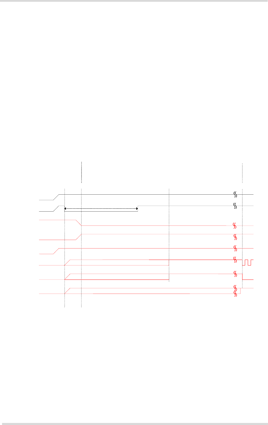
3.3.1
Turn on PCS3
When the PCS3 module is in Power-down mode, it can be started to Normal mode by driving
the IGT (ignition) line to ground. it is recommended to use an open drain/collector driver to
avoid current flowing into this signal line. Pulling this signal low triggers a power-on sequence.
To turn on PCS3 IGT has to be kept active at least 100ms. After turning on PCS3 IGT should
be set inactive to prevent the module from turning on again after a shut down by AT command
or EMERG_OFF. For details on signal states during startup see also Section 3.3.2 and Section
3.10.6.
IGT
Power
supply
active
Module
Firmware start up, command interface initialization
Function
active
0ms ~28ms ~5s
BATT+
IGT
PWR_IND
>100ms
VEXT
EMERG_OFF
ASC0
CTS0
USB*
Initial state
Initial state
Undefined state
Intermediate state
Intermediate state
* USB interface may take up to 5s to reach its active state (typ. 4s)
Figure 4: Power-on with IGT
Note: After power up IGT should remain high. Also note that with a USB connection the USB
host may take more than 5 seconds to set up the virtual COM port connection.
After startup or mode change the following URCs sent to every port able to receive AT com-
mands indicating the module’s ready state:
•
"^SYSSTART" indicates that the module has entered Normal mode.
•
"^SYSSTART AIRPLANE MODE" indicates that the module has entered Airplane mode.
These URCs notify the external application that the first AT command can be sent to the mod-
ule. If these URCs are not used to detect then the only way of checking the module’s ready
state is polling. To do so, try to send characters (e.g. “at”) until the module is responding.

PCS3_HD_v01.000-03
Confidential / Preliminary Page 26 of 101 2013-10-21
PCS3 Hardware Interface Description
3.3 Power-Up / Power-Down Scenarios
3.3.2
Signal States after Startup
Table 7 describes the various states each interface signal passes through after startup and dur-
ing operation.
Signals are in an initial state while the module is initializing. Once the startup initialization has
completed, i.e. when the software is running, all signals are in defined state. The state of sev-
eral signals will change again once the respective interface is activated or configured by AT
command (for more information see also Section 3.10.6).
Table 7: Signal states
Signal name Power on reset
Duration appr. 150ms
Startup phase
Duration appr. 4s
State after first
firmware initialization
After 4-4.5s
RXD0 PD PU O, H
TXD0 PD PD I, PD
CTS0 PD PU O, L
RTS0 PD PD I, PD
DTR0 PD PU I, PU
DCD0 PD PU1 O, H
DSR0 PU PU O, L
RING0 PU PU O, H
WAKEUP PD PD PD
LCI_IND PD PD PD
PWR_IND O, L O, L O, L
STATUS PD PD PD
PCM PD PD PD
1.
No external pull down allowed during this phase.
L = Low level
H = High level
I = Input
O = Output
PD = Pull down resistor with appr. 100k
PD(…k) = Pull down resistor with ...k
PU = Pull up resistor with appr. 100k
PU(…k) = Pull up resistor with ...k
PCS3_HD_v01.000-03
Confidential / Preliminary Page 27 of 101 2013-10-21
PCS3 Hardware Interface Description
3.3 Power-Up / Power-Down Scenarios
3.3.3
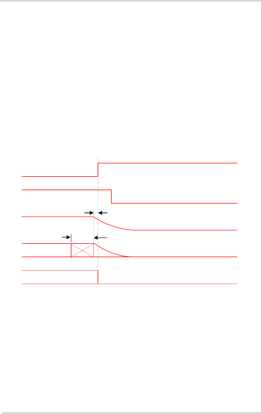
Turn off PCS3 Using AT Command
The best and safest approach to powering down PCS3 is to issue the AT^SMSO command.
This procedure lets PCS3 log off from the network and allows the software to enter into a secure
state and safe data before disconnecting the power supply. The mode is referred to as Power
Down mode. In this mode, only the RTC stays active. After sending AT^SMSO do not enter any
other AT commands. To verify that the module turned off it is possible to monitor the PWR_IND
signal. A high state of the PWR_IND signal line definitely indicates that the module is switched
off.
Be sure not to disconnect the supply voltage VBATT+ before the module has been switched off
and the PWR_IND signal has gone high. Otherwise you run the risk of losing data.
While PCS3 is in Power-down mode the application interface is switched off and must not be
fed from any other source. Therefore, your application must be designed to avoid any current
flow into any digital signal lines of the application interface, especially of the serial interfaces.
No special care is required for the USB interface which is protected from reverse current.
Power down
PWR_IND
BATT+ See note 1
VEXT
0.5ms
See note 2
approx.
12ms
Digital outputs
Reset
State
Digital inputs driven by application
Figure 5: Signal states during turn-off procedure
Note 1: The power supply voltage (BATT+) may be disconnected resp. switched off only after
having reached Power Down mode as indicated by the PWR_IND signal going high.
Note 2: Depending on capacitance load from host application.
Note 3: After module shutdown by means of AT command, please allow for a time period of at
least 1s before restarting the module.
PCS3_HD_v01.000-03
Confidential / Preliminary Page 28 of 101 2013-10-21
PCS3 Hardware Interface Description
3.3 Power-Up / Power-Down Scenarios
3.3.4
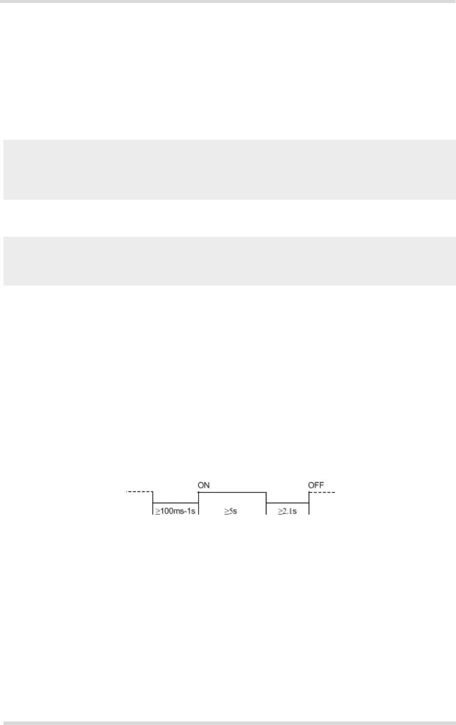
Configuring the IGT Line for Use as ON/OFF Switch
The IGT line can be configured for use in two different switching modes: You can set the IGT
line to switch on the module only, or to switch it on and off. The switching mode is determined
by the parameter "MEShutdown/OnIgnition" of the AT^SCFG command. This approach is use-
ful for application manufacturers who wish to have an ON/OFF switch installed on the host de-
vice.
By factory default, the ON/OFF switch mode of IGT is disabled:
at^scfg=meshutdown/onignition
^SCFG: "MEShutdown/OnIgnition","off"
OK
# Query the current status of IGT.
# IGT can be used only to switch on PCS3.
IGT works as described in Section 3.3.1.
To configure IGT for use as ON/OFF switch:
at^scfg=meshutdown/onignition
^SCFG: "MEShutdown/OnIgnition","on"
OK
# Enable the ON/OFF switch mode of IGT.
# IGT can be used to switch on and off PCS3.
We strongly recommend taking great care before changing the switching mode of the IGT line.
To ensure that the IGT line works properly as ON/OFF switch it is of vital importance that the
following conditions are met.
Switch-on condition: If the PCS3 is off, the IGT line must be asserted for at least 100ms before
being released.
Switch-off condition: If the PCS3 is on, the IGT line must be asserted for at least 2.1s before
being released. The module switches off after the line is released. The
switch-off routine is identical with the procedure initiated by AT^SMSO, i.e.
the software performs an orderly shutdown as described in Section 3.3.3.
Before switching off the module wait at least 5 seconds after startup.
Figure 6: Timing of IGT if used as ON/OFF switch

PCS3_HD_v01.000-03
Confidential / Preliminary Page 29 of 101 2013-10-21
PCS3 Hardware Interface Description
3.3 Power-Up / Power-Down Scenarios
3.3.5
Automatic Shutdown
Automatic shutdown takes effect if:
•
The PCS3 board is exceeding the critical limits of overtemperature or undertemperature
•
Undervoltage or overvoltage is detected
The automatic shutdown procedure is equivalent to the power down initiated with the AT^SMSO
command, i.e. PCS3 logs off from the network and the software enters a secure state avoiding
loss of data.
Alert messages transmitted before the device switches off are implemented as Unsolicited Re-
sult Codes (URCs). The presentation of the temperature URCs can be enabled or disabled with
the AT commands AT^SCTM. The URC presentation mode varies with the condition, please
see Section 3.3.5.1 to Section 3.3.5.3 for details. For further instructions on AT commands refer
to [1].

PCS3_HD_v01.000-03
Confidential / Preliminary Page 30 of 101 2013-10-21
PCS3 Hardware Interface Description
3.3 Power-Up / Power-Down Scenarios
3.3.5.1
Thermal Shutdown
The board temperature is constantly monitored by an internal NTC resistor located on the PCB.
The values detected by the NTC resistor are measured directly on the board and therefore, are
not fully identical with the ambient temperature.
Each time the board temperature goes out of range or back to normal, PCS3 instantly displays
an alert (if enabled).
•
URCs indicating the level "1" or "-1" allow the user to take appropriate precautions, such as
protecting the module from exposure to extreme conditions. The presentation of the URCs
depends on the settings selected with the AT^SCTM write command:
AT^SCTM=1: Presentation of URCs is always enabled.
AT^SCTM=0 (default): Presentation of URCs is enabled during the 15 second guard period
after start-up of PCS3. After expiry of the 15 second guard period, the presentation will be
disabled, i.e. no URCs with alert levels "1" or ''-1" will be generated.
•
URCs indicating the level "2" or "-2" are instantly followed by an orderly shutdown. The pre-
sentation of these URCs is always enabled, i.e. they will be output even though the factory
setting AT^SCTM=0 was never changed.
The maximum temperature ratings are stated in Section 6.2. Refer to Table 8 for the associated
URCs.
Table 8: Temperature dependent behavior
Sending temperature alert (15sec after PCS3 start-up, otherwise only if URC presentation enabled)
^SCTM_B: 1 Caution: Board close to over temperature limit, i.e., board is 5°C below over
temperature limit.
^SCTM_B: -1 Caution: Board close to under temperature limit, i.e., board is 5°C above under-
temperature limit.
^SCTM_B: 0 Board back to uncritical temperature range, i.e., board is 6°C below its over- or
above its under temperature limit.
Automatic shutdown (URC appears no matter whether or not presentation was enabled)
^SCTM_B: 2 Alert: Board equal or beyond over temperature limit. PCS3 switches off.
^SCTM_B: -2 Alert: Board equal or below under temperature limit. PCS3 switches off.
The AT^SCTM command can also be used to check the present status of the board. Depending
on the selected mode, the read command returns the current board temperature in degrees
Celsius or only a value that indicates whether the board is within the safe or critical temperature
range. See [1] for further instructions.

PCS3_HD_v01.000-03
Confidential / Preliminary Page 31 of 101 2013-10-21
PCS3 Hardware Interface Description
3.3 Power-Up / Power-Down Scenarios
3.3.5.2
Under voltage Shutdown
If the measured battery voltage is no more sufficient to set up a call the following URC will be
presented: ^SBC: Under voltage.
The URC indicates that the module is close to the under voltage threshold. If under voltage
persists the module keeps sending the URC several times before switching off automatically.
This type of URC does not need to be activated by the user. It will be output automatically when
fault conditions occur.
3.3.5.3
Over voltage Shutdown
The overvoltage shutdown threshold is 100mV above the maximum supply voltage VBATT+
specified in Table 22.
When the supply voltage approaches the overvoltage shutdown threshold the module will send
the following URC:
^SBC: Overvoltage warning
This alert is sent once.
When the overvoltage shutdown threshold is exceeded the module will send the following URC
^SBC: Overvoltage shutdown
before it shuts down cleanly:
This type of URC does not need to be activated by the user. It will be output automatically when
fault conditions occur.
Keep in mind that several PCS3 components are directly linked to BATT+ and, therefore, the
supply voltage remains applied at major parts of PCS3, even if the module is switched off.
Especially the power amplifier is very sensitive to high voltage and might even be destroyed.
3.3.6
Automatic Reset
An automatic reset takes effect if
•
A sudden momentary power loss (SMPL) occurs - e.g., a very brief battery disconnect - and
the power returns within 2 seconds.
The SMPL feature ensures that if VBATT+ drops out-of-range (< 2.55V nominal) and then re-
turns into range within 2 seconds, the power-on sequence is executed and the module switches
on again. Thus the SMPL feature achieves immediate and automatic recovery from momentary
power loss such as a brief battery disconnect.
To employ the SMPL feature the VDDLP line has to supplied for at least 2 seconds after a
possible power loss (e.g., by connecting a 10µF capacitor).
PCS3_HD_v01.000-03
Confidential / Preliminary Page 32 of 101 2013-10-21
PCS3 Hardware Interface Description
3.3 Power-Up / Power-Down Scenarios
3.3.7
Turn off PCS3 in Case of Emergency
Caution: Use the EMERG_OFF line only when, due to serious problems, the software is not
responding for more than 5 seconds. Pulling the EMERG_OFF line causes the loss of all
information stored in the volatile memory. Therefore, this procedure is intended only for use in
case
of emergency, e.g. if PCS3 does not respond, if reset or shutdown via AT command fails.
The EMERG_OFF line is available on the application interface and can be used to switch off
the module. To control the EMERG_OFF line it is recommended to use an open drain / collector
driver.
To switch off, the EMERG_OFF line must be pulled to ground for longer than 40ms. After the
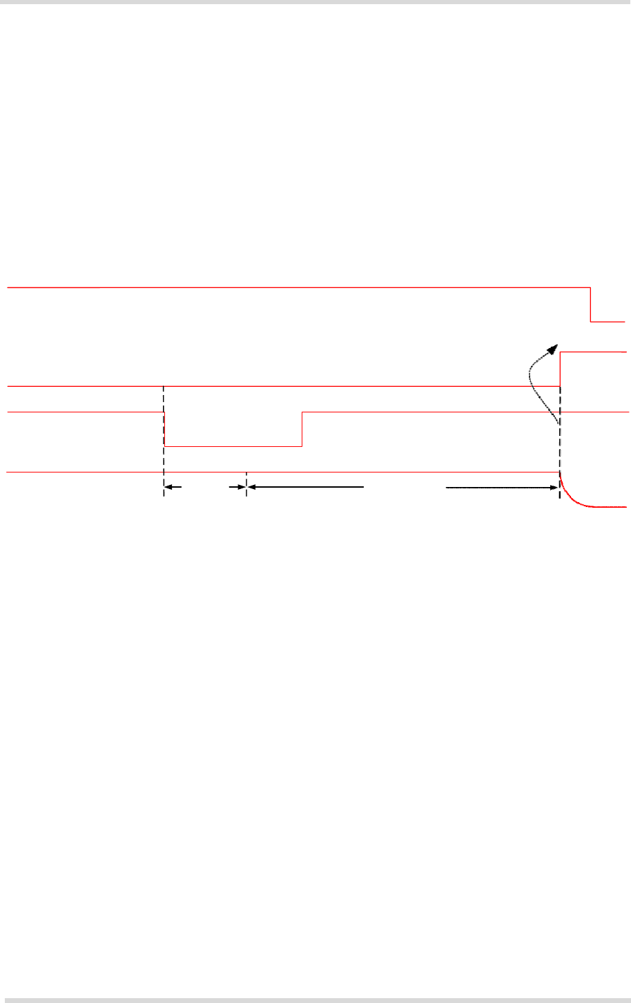
40ms and an additional delay period of 500ms the module shuts down as shown in Figure 7.
BATT+
Shut Down
PWR_IND
EMERG_OFF >40ms
VEXT 40ms 500ms
Figure 7: Shutdown by EMERG_OFF signal
Please note that the power supply voltage (BATT+) may be disconnected resp. switched off
only after having reached Shut Down as indicated by the PWR_IND signal going high. The
power supply has to be available (again) before the module is restarted.

PCS3_HD_v01.000-03
Confidential / Preliminary Page 33 of 101 2013-10-21
PCS3 Hardware Interface Description
3.4 Power Saving
3.4
Power Saving
PCS3 is able to reduce its functionality to a minimum (during the so-called SLEEP mode) in
order to minimize its current consumption. The following sections explain the module’s CTS0
behavior and also mention how to wake up from or disable the so-called SLEEP mode.
The implementation of the USB host interface also influences the module’s power saving
behavior and therefore its current consumption. For more information see Section 3.6.
Note. The module’s SLEEP mode current consumption can be reduced significantly (0.8mA)
by enabling the VEXT power save mode. Hence, it is recommended to enable power saving on
VEXT if at all possible. For more information see Table 22: VEXT.
Another feature influencing the current consumption is the configuration of the GNSS antenna
interface. For details see Section 6.9.
3.4.1
Power Saving while Attached to CDMA Networks
The so-called slotted paging in CDMA is similar to the WCDMA paging timing cycles for power
saving.
During normal CDMA operation, i.e., the module is connected to a CDMA network, the duration
of a power saving period varies. It may be calculated using the following formula:
T=2i * 1.28s (16 slots of 80ms)
The slot cycle index i is determined by the CDMA network and can be an integer between -4
to 7 inclusive. The typical value is 2. Therefore, the typical power saving period would be
(22)*1.28s = 5.12s.
3.4.2
Timing of the CTS0 Signal, CDMA
As long as PCS3 is operated via the ASC0 interface and not in power saving mode, the CTS0
line is always active. This means that while attached to a network the CTS0 signal will be tem
poraly active during each paging.
After a concluding activity on the serial interface ASC0 - and depending on the module’s other
activities - it takes by default 5 seconds before CTS0 goes inactive (again) and power saving
starts. The 5 second delay period can be configured using the AT^SCFG parameter "MEop-
Mode/PwrSave", <PwrSaveDelay> (see [1]).
With regard to programming or using timeouts, the UART must take the varying CTS0 inactivity
periods into account.
Note: Hardware handshaking is mandatory if employing PCS3’s ASC0 interface with enabled
power saving. Thus AT commands are only recognized by the module while CTS0 is active.

PCS3_HD_v01.000-03
Confidential / Preliminary Page 34 of 101 2013-10-21
PCS3 Hardware Interface Description
3.4 Power Saving
3.4.3
Wake up from or Disabling Power Saving
The RTS0 line can be used to wake up the module from its power saving SLEEP mode. RTS0
activation (high to low transition) may be employed to cut short pauses between listening to
paging messages. Following an RTS toggle the module will return to SLEEP mode 5 seconds
after the last character was sent over the interface. This default delay period can be configured
using the AT^SCFG parameter "MEopMode/PwrSave", <PwrSaveDelay>.
If not regularly woken up from power saving (through network requirements or by means of
RTS toggling as described above), the power saving timeout recommended for the AT^SCFG
parameter "MEopMode/PwrSave", <PwrSaveTimeout> ensures that the module regularly
wakes up from its power saving state (SLEEP mode). It is recommended to configure a regular
module wake up, especially if the radio interface is switched off (Airplane mode) and the mod-
ule is connected via serial interface (i.e., AT^SDPORT=2) to an external application without di-
rect access to its RTS0 line (e.g., an application using standard Windows/Linux serial device
drivers).
The AT^SCFG parameter "MEopMode/PwrSave", <PwrSaveMode> can be used to disable
power saving completely, i.e., the module will no longer enter SLEEP mode but remain in IDLE
mode instead. Please note that if this setting is used to avoid implementing hardware hand-
shaking on ASC0, it is mandatory to have RTS0 pulled down or left open (an internal pull down
is available).
For more information on power saving and the appropriate AT^SCFG parameters to configure
the power save behavior see [1].
PCS3_HD_v01.000-03
Confidential / Preliminary Page 35 of 101 2013-10-21
PCS3 Hardware Interface Description
3.5 RTC Backup
SMT
inte
r
face
3.5
RTC Backup
The internal Real Time Clock of PCS3 is supplied from a separate voltage regulator in the pow-
er supply component which is also active when PCS3 is in Power Down mode and BATT+ is
available.
In addition, you can use the VDDLP line on the SMT interface to backup the RTC from an ex-
ternal capacitor or a battery (rechargeable or non-chargeable). The capacitor is charged from
the internal LDO of PCS3. If the voltage supply at BATT+ is disconnected the RTC can be pow-
ered by the capacitor. The size of the capacitor determines the duration of buffering when no
voltage is applied to PCS3, i.e. the greater the capacitor the longer PCS3 will save the date and
time. It limits the output current of an empty capacitor or battery.
Figure 8 show various sample configurations.
Module
Non chargeable battery
BATT+
Chargeable battery
Capacitor
3.2V
LDO
0.8k
1k
VDDLP
or or
Processor and power
management
RTC
GND
Figure 8: RTC supply variants
PCS3_HD_v01.000-03
Confidential / Preliminary Page 36 of 101 2013-10-21
PCS3 Hardware Interface Description
3.6 USB Interface
3.6
USB Interface
PCS3 supports a USB 2.0 Full Speed (12Mbit/s)
compliant. The USB interface is primarily
intended for use as command and data interface and
for downloading firmware.
The external application is responsible for supplying the VUSB_IN line. This line is used for ca-
ble detection only. The USB part (driver and transceiver) is supplied by means of BATT+. This
is because PCS3 is designed as a self-powered device compliant with the “Universal Serial Bus
Specification Revision 2.0”1.
Module
USB part1)
VREG (3.8V)
lin. reg.
SMT
BATT+
GND
VBUS
DP
DN
Detection only
RS
RS
VUSB_IN
USB_DP2)
USB_DN2)
Host wakeup
RING0
WAKEUP
1)
All serial (including R
S
)and pull-up resistors for data lines are implemented.
2)
The USB interface is operated in
Full Speed (12Mbit/s)
, it is recommended to take
special
care routing the data lines USB_DP and USB_DN. Application layout should in this
case implement a differential impedance of 90Ohm for proper signal integrity.
Figure 9: USB circuit
To properly connect the module's USB interface to the external application, a USB 2.0 compat-
ible connector and cable or hardware design is required. For more information on the USB re-
lated electrical signals see Table 22.
1. The specification is ready for download on http://www.usb.org/developers/docs/

PCS3_HD_v01.000-03
Confidential / Preliminary Page 37 of 101 2013-10-21
PCS3 Hardware Interface Description
3.6 USB Interface
3.6.1
Reducing Power Consumption
While a USB connection is active, the module will never switch into SLEEP Mode. Only if the
USB interface is in Suspended state or Detached (i.e., VUSB_IN = 0) is the module able to
switch into SLEEP mode thereby saving power. There are two possibilities to enable power re-
duction mechanisms:
•
Recommended implementation of USB Suspend/Resume/Remote Wakeup:
The USB host should be able to bring its USB interface into the Suspended state as
described in the “Universal Serial Bus Specification Revision 2.0“1. For this functionality to
work, the VUSB_IN line should always be kept enabled. On incoming calls and other events
PCS3 will then generate a Remote Wakeup request to resume the USB host controller.
See also [5] (USB Specification Revision 2.0, Section 10.2.7, p.282):
"If USB System wishes to place the bus in the Suspended state, it commands the Host Con-
troller to stop all bus traffic, including SOFs. This causes all USB devices to enter the Sus-
pended state. In this state, the USB System may enable the Host Controller to respond to
bus wakeup events. This allows the Host Controller to respond to bus wakeup signaling to
restart the host system."
•
Implementation for legacy USB applications not supporting USB Suspend/Resume:
As an alternative to the regular USB suspend and resume mechanism it is possible to
employ the RING0 or WAKEUP line to wake up the host application in case of incoming
calls or events signalized by URCs while the USB interface is in Detached state (i.e.,
VUSB_IN = 0). Every wakeup event will force a new USB enumeration. Therefore, the
external application has to carefully consider the enumeration timings to avoid loosing any
signalled events. For details on this host wakeup functionality see Section 3.10.4.
1.
The specification is ready for download on http://www.usb.org/developers/docs/
PCS3_HD_v01.000-03
Confidential / Preliminary Page 38 of 101 2013-10-21
PCS3 Hardware Interface Description
3.7 Serial Interface ASC0
3.7
Serial Interface ASC0
PCS3 offers an 8-wire unbalanced, asynchronous modem interface ASC0 conforming to ITU-
T V.24 protocol DCE signalling. The electrical characteristics do not comply with ITU-T V.28.
The significant levels are 0V (for low data bit or active state) and 1.8V (for high data bit or in-
active state). For electrical characteristics please refer to Table 22. For an illustration of the in-
terface line’s startup behavior see Section 3.10.6.
PCS3 is designed for use as a DCE. Based on the conventions for DCE-DTE connections it
communicates with the customer application (DTE) using the following signals:
•
Port TXD @ application sends data to the module’s TXD0 signal line
•
Port RXD @ application receives data from the module’s RXD0 signal line
Figure 10: Serial interface ASC0
Features:
•
Includes the data lines TXD0 and RXD0, the status lines RTS0 and CTS0 and, in addition,
the modem control lines DTR0, DSR0, DCD0 and RING0.
•
ASC0 is designed for controlling voice calls, transferring data and for controlling the module
with AT commands.
•
Full multiplexing capability allows the interface to be partitioned into virtual channels.
•
The RING0 signal serves to indicate incoming calls and other types of URCs (Unsolicited
Result Code). It can also be used to send pulses to the host application, for example to
wake up the application from power saving state. See [1] for details on how to configure the
RING0 line by AT^SCFG.
•
Configured for 8 data bits, no parity and 1 stop bit.
•
ASC0 can be operated at fixed bit rates from 9600bps up to 921600bps.
•
Supports RTS0/CTS0 hardware flow control.
•
Wake up from SLEEP mode by RTS0 activation (high to low transition).
Note. If the ASC0 serial interface is the application’s only interface, it is suggested to connect
test points on the USB signal lines as a potential tracing possibility.

PCS3_HD_v01.000-03
Confidential / Preliminary Page 39 of 101 2013-10-21
PCS3 Hardware Interface Description
3.7 Serial Interface ASC0
Table 9: DCE-DTE wiring of ASC0
V.24 circuit DCE DTE
Line function Signal direction Line function Signal direction
103 TXD0 Input TXD Output
104 RXD0 Output RXD Input
105 RTS0 Input RTS Output
106 CTS0 Output CTS Input
108/2 DTR0 Input DTR Output
107 DSR0 Output DSR Input
109 DCD0 Output DCD Input
125 RING0 Output RING Input

PCS3_HD_v01.000-03
Confidential / Preliminary Page 40 of 101 2013-10-21
PCS3 Hardware Interface Description
3.8 Analog Audio Interface
3.8
Analog Audio Interface
PCS3 has an analog audio interface with a balanced analog microphone input and a balanced
analog earpiece output. A supply voltage and an analog ground connection are provided at
dedicated lines.
PCS3 offers eight audio modes which can be selected with the AT^SNFS command. The elec-
trical characteristics of the voiceband part vary with the audio mode. For example, sending and
receiving amplification, sidetone paths, noise suppression etc. depend on the selected mode
and can in parts be altered with AT commands (except for mode 1).
Please refer to Section 6.7 for specifications of the audio interface and an overview of the audio
parameters. Detailed instructions on using AT commands are presented in [1]. Table 25 sum-
marizes the characteristics of the various audio modes and shows what parameters are sup-
ported in each mode.
When shipped from factory, all audio parameters of PCS3 are set to audio mode 1. This is the
default configuration optimized for the Votronic HH-SI-30.3/V1.1/0 handset and used for type
approving the Cinterion Wireless Modules reference configuration. Audio mode 1 has fix pa-
rameters which cannot be modified. To adjust the settings of the Votronic handset simply
change to another audio mode.
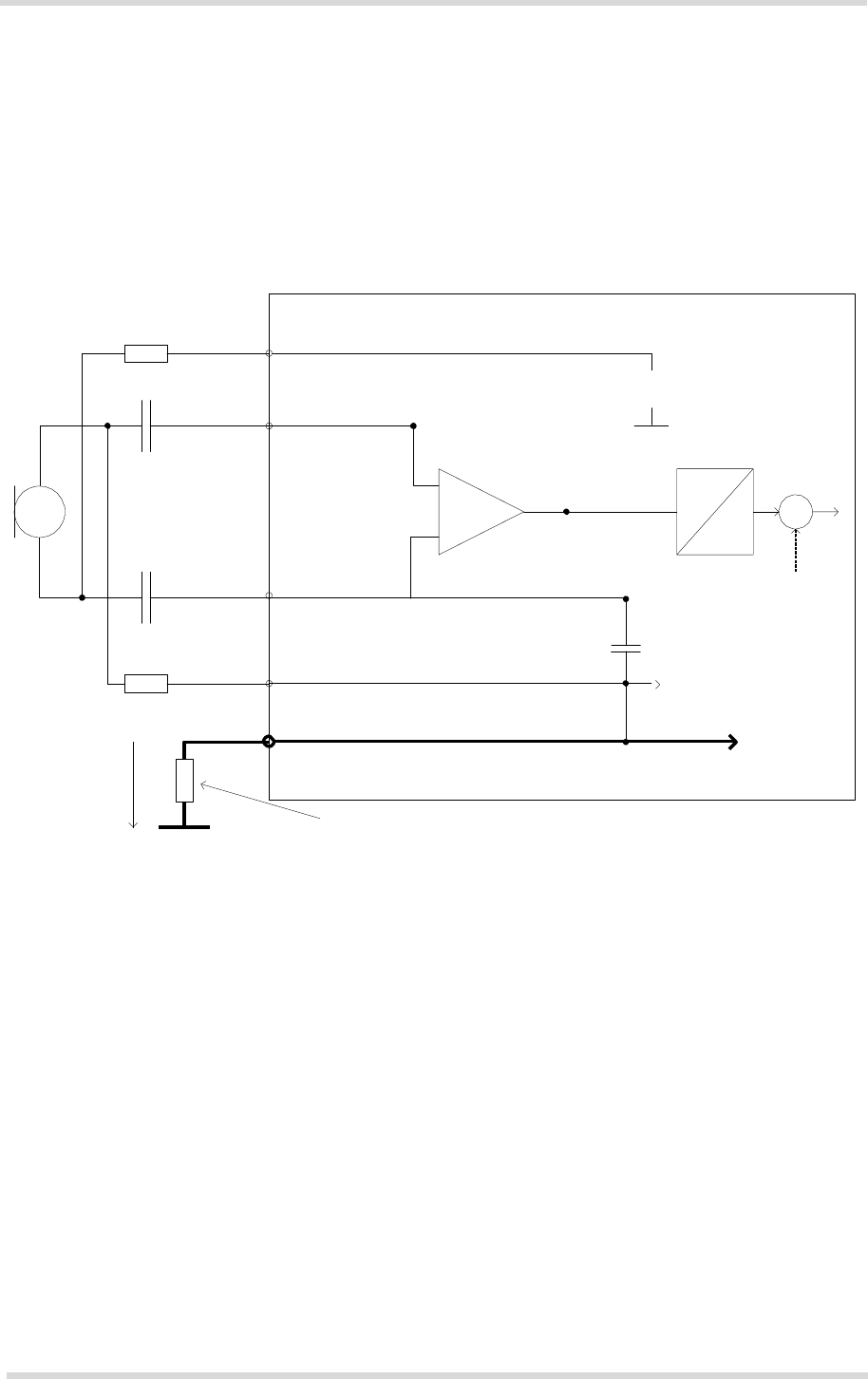
PCS3_HD_v01.000-03
Confidential / Preliminary Page 41 of 101 2013-10-21
PCS3 Hardware Interface Description
3.8 Analog Audio Interface
3.8.1
Microphone Inputs and Supply
The differential microphone inputs MICP and MICN present variable impedances depending
on the gain. The microphone inputs must be decoupled by capacitors Ck (typical 1µF). The in-
put stage uses a differential operational amplifier circuit with programmable resistors in the in-
put and the feedback path. The detailed structure of this stage and the following uplink path is
shown in Figure 11. The input can be controlled by the AT command AT^SNFI. Command pa-
rameters with their effect are mentioned in the figure and marked in <red>. More information
about audio AT commands can be found in Section 6.7 and [1].
Module
Rs VMIC
Ck
MICN
<micAmp1> 0dBm
or 24dBm
VMIC
AGND
-
A PCM
X
Ck
MICP
Rs AGND
AGND
D
<micTxVol>
GND
GND Line leading burst current
GND
V Noise
Application GND
Connection Resistance
Figure 11: Structure of Audio Input and Supply

PCS3_HD_v01.000-03
Confidential / Preliminary Page 42 of 101 2013-10-21
PCS3 Hardware Interface Description
3.8 Analog Audio Interface
MICP leads the signal via to the non-inverting input of the operational amplifier
which is then
connected via to AGND. The gain of
the input stage can be programmed by the parameter
<micAmp1>, A gain stage follows that can be set to 0dB or 24dB using <micAmp1>. If 24dB is
spec-
ified, the common mode rejection ratio is reduced accordingly.
Finally, the uplink gain can be scaled in the PCM path by the <micTxVol> parameter.
It is recommended to use the AGND line for grounding the microphone circuit. AGND provides
for the same module ground potential the analog circuits of the module refer to. AGND must
not be connected to the system GND anywhere. Otherwise high burst peak currents may flow
across AGND causing humming in the uplink audio signal.
A regulated power supply for electret microphones is available at VMIC. The voltage at VMIC
is rated at 1.8V at 3mA and is available while audio is active (e.g., during a call).
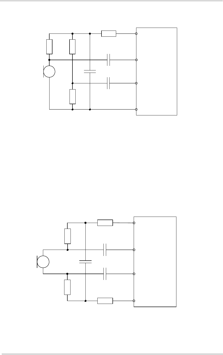
PCS3_HD_v01.000-03
Confidential / Preliminary Page 43 of 101 2013-10-21
PCS3 Hardware Interface Description
3.8 Analog Audio Interface
The following figures show possible microphone and line connections.
470
VMIC
2k2 2k2
5k6
+
10µF
1µF
1µF
MICP
MICN
Module
AGND
Figure 12: Single ended microphone connection
The configuration shown in Figure 12 is suitable for short distances between microphone and
module. A typical electric microphone has a metal case connected to its ground pad. Since this
is routed directly to AGND, electro static discharges applied to the microphone will be easily
led away. It is recommended to use an additional RC-filter for VMIC (for example 470 Ohm and
10µF as shown in the figure) in case a high microphone gain is necessary.
If the microphone lines are longer, use the configuration shown in Figure 13. It is recommended
to use an additional RC-filter for VMIC (for example 1kOhm, 10µF and 1kOhm as shown in the
figure) in case a high microphone gain is necessary.
1k VMIC
1k
1µF
MICP
+
10µF
MICN
Module
1µF
1k
1k
AGND
Figure 13: Differential microphone connection
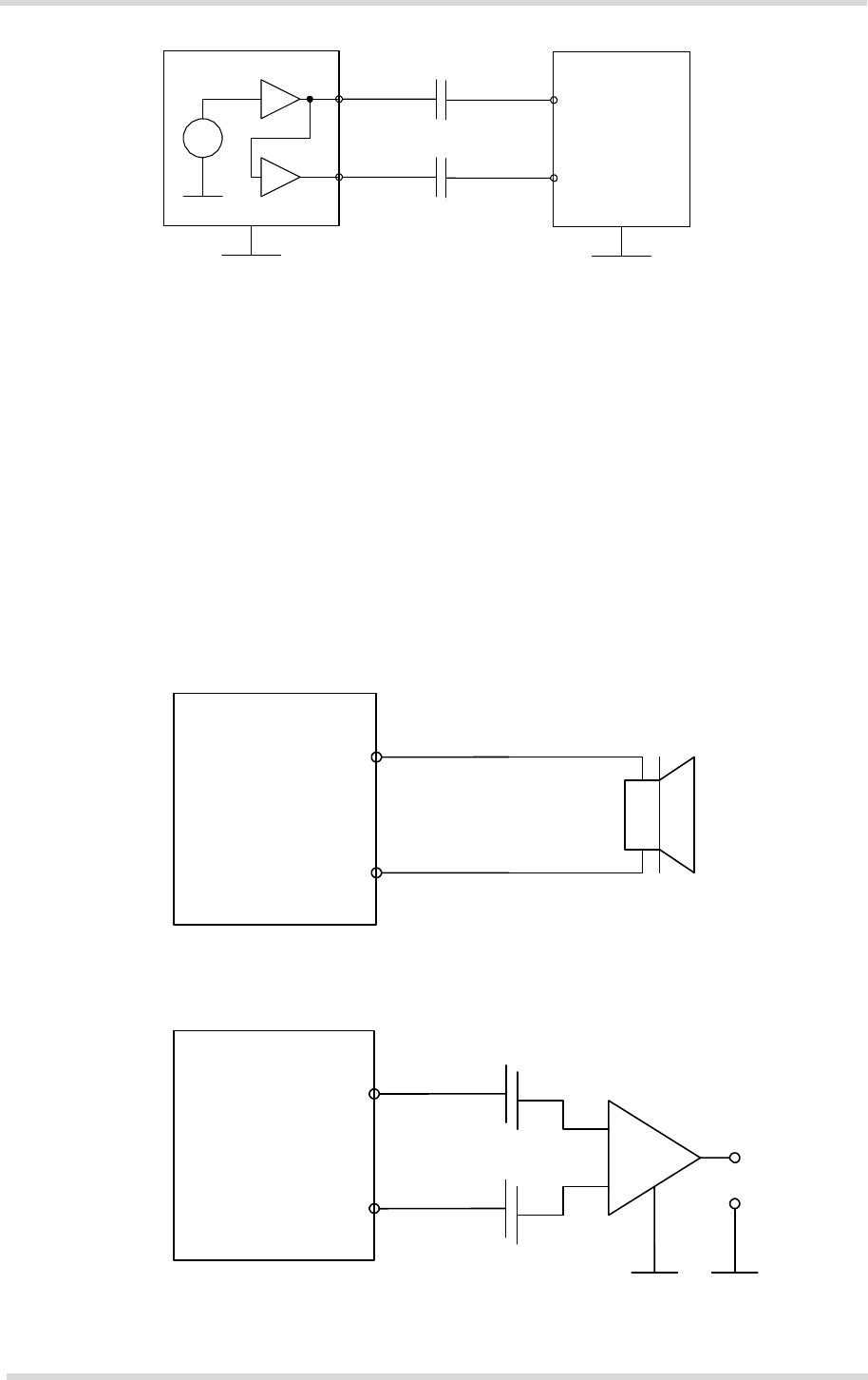
PCS3_HD_v01.000-03
Confidential / Preliminary Page 44 of 101 2013-10-21
PCS3 Hardware Interface Description
3.8 Analog Audio Interface
Line output device
100nF
MICP
~
-1 MICN
Module
100nF
Figure 14: Line input
Using the line input configuration the output level of the ground related balanced source should
be as high as possible to achieve the best SNR. Since the input impedance of PCS3 is quite
high at low gains, the coupling capacitances may be smaller.
3.8.2
Loudspeaker Output
PCS3 provides a differential loudspeaker output EPP/EPN. If it is used as line output, the ap-
plication should provide a capacitor decoupled differential input to eliminate humming. A single
ended connection to a speaker or a line input is strongly not recommended.
The following figures show the typical output configurations.
EPP
Module
EPN
Figure 15: Differential loudspeaker connection
Module
EPP
+
_
EPN
Figure 16: Line output connection
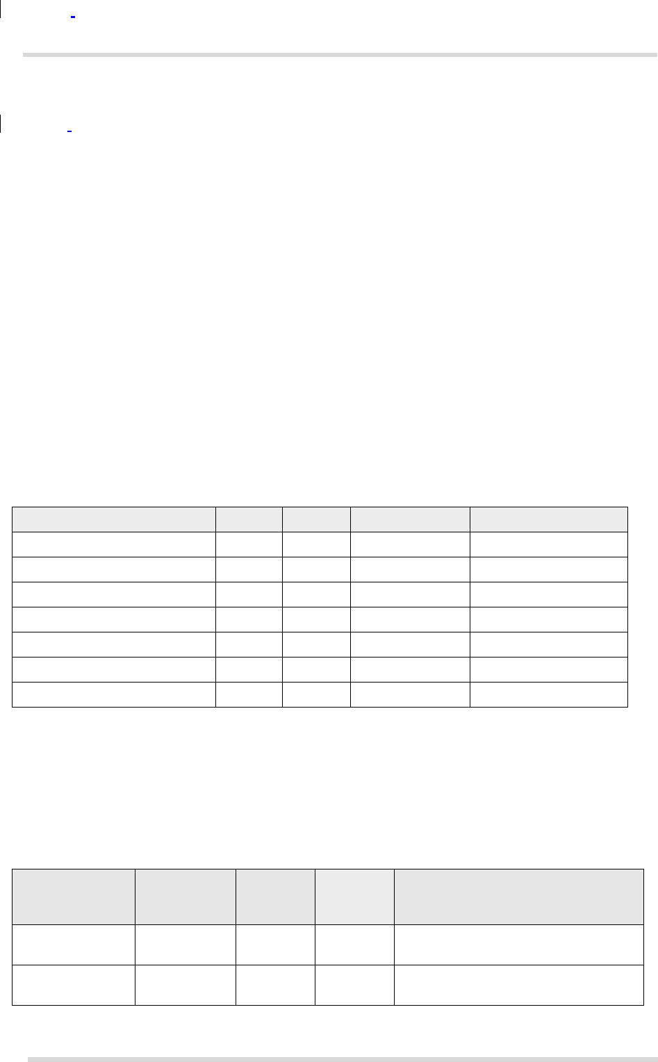
PCS3_HD_v01.000-03
Confidential / Preliminary Page 45 of 101 2013-10-21
PCS3 Hardware Interface Description
3.9 Digital Audio Interface
3.9
Digital Audio Interface
PCS3 supports a digital audio interface that can be employed either as pulse code modulation
(see Section 3.9.1) or as inter IC sound interface (see Section 3.9.2). Operation of these inter-
face variants is mutually exclusive.
3.9.1
Pulse Code Modulation Interface (PCM)
PCS3’s PCM interface can be used to connect audio devices capable of pulse code modula-
tion. The PCM functionality allows the use of a codec like the Freescale MC145483. Using the
AT^SAIC command you can activate and configure the PCM interface (see [1]).
The PCM interface supports the following modes:
•
Master mode, slave mode
•
Short frame synchronization
•
256kHz, 512kHz and 2048kHz bit clock
•
Additional master mode with 128kHz, long frame synchronization
For the PCM interface configuration the parameters <clock>, <mode> <frame_mode> and
<ext_clk_mode> of the AT^SAIC command can be configured. The following table lists possi-
ble combinations:
Table 11: Configuration combinations for the PCM interface
Configuration <clock> <mode> <frame_mode> <ext_clk_mode>
Master, 128kHz, long frame 0 0 1 0 or 1
Master, 256kHz, short frame 1 0 0 0 or 1
Master, 512kHz, short frame 2 0 0 0 or 1
Master, 2048kHz, short frame 3 0 0 0 or 1
Slave, 256kHz, short frame 1 1 0 1
Slave, 512kHz, short frame 2 1 0 1
Slave, 2048kHz, short frame 3 1 0 1
In slave mode <clock> must be set according the source clock frequency. Being in master
mode clock and frame synchronization signals may be permanently switched on by
<ext_clk_mode> parameter. These signals may be used for clocking digital audio periphery
outside a call.
Table 12 lists the available PCM interface signals.
Table 12: Overview of PCM signal functions
Signal name on
SMT application
interface
Signal
configuration
inactive1
Signal
direction:
Master
Signal
direction:
Slave
Description
PCM_OUT PD O O PCM Data from PCS3 to external
codec
PCM_IN PD I I PCM Data from external codec to
PCS3
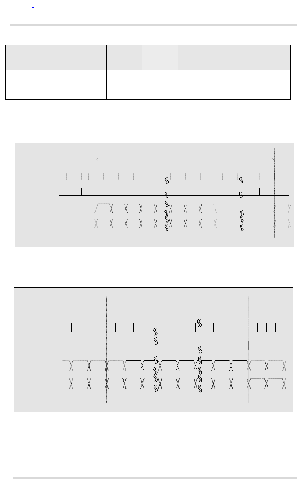
PCS3_HD_v01.000-03
Confidential / Preliminary Page 46 of 101 2013-10-21
PCS3 Hardware Interface Description
3.9 Digital Audio Interface
125 µs
MSB
14
13
12
2
1
LSB
MSB
MSB
14
13
12
2
1
LSB
MSB
Table 12: Overview of PCM signal functions
Signal name on
SMT application
interface
Signal
configuration
inactive1
Signal
direction:
Master
Signal
direction:
Slave
Description
PCM_FSC PD O I Frame synchronization signal to/from
external codec
PCM_CLK PD O I Bit clock to/from external codec
1.
Inactive means no call, no tone generation and no external clock mode. PD = Pull down
The timing of a PCM short frame is shown in Figure 17. The timing for master and slave mode
is identical, except for the PCM_FSC and PCM_CLK signal direction (see Table 12).
PCM_CLK
PCM_FSC
PCM_OUT
PCM_IN
Figure 17: PCM timing short frame (External codec 2048KHz)
The timing of a PCM long frame for the additional 128kHz master mode is shown in Figure 18.
PCM_CLK
PCM_FSC
PCM_OUT
PCM_IN
1 LSB
1 LSB
MSB
MSB
14 13 8 7
14 13 8 7
2 1 LSB
2 1
LSB
MSB 14
MSB 14
Figure 18: PCM timing long frame (master, 128kHz)
Please note that PCM data is always formatted as 16-bit uncompressed two’s complement. Al-
so, all PCM data and frame synchronization signals are written to the PCM bus on the rising
clock edge and read on the falling edge.
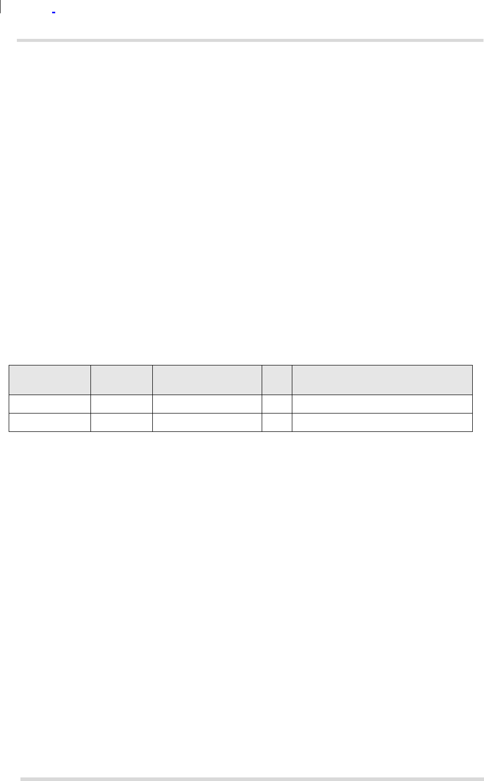
PCS3_HD_v01.000-03
Confidential / Preliminary Page 47 of 101 2013-10-21
PCS3 Hardware Interface Description
3.9 Digital Audio Interface
3.9.2
I2C Interface
PCS3’s I2C compatible interface for FM radio support and Camera
I2C_SDA and I2C_SCL: I2C control bus Serial data line of the I2C bus (I2C_SDA) – the
standard required pull-up resistor is placed on the QSC device side; a pull-up resistor is not
required in the camera module. Serial clock line of the I2C bus (I2C_SCL) – the standard
required pull-up resistor is placed on the QSC device side; a pull-up resistor is not required in
the camera module.
The I2C interface features and limitation:
Two-wire bus for inter-IC communication
Support for external devices fabricated using any process (1.8 V only)
Support for external functions such as camera sensors, microcontrollers, FM radio ICs, LCD
driver, stereo DAC, and keyboard interface
Two operating modes with different transfer rates
Standard-mode: up to ~100 kbps
Fast-mode: up to ~400 kbps
The controller functions only as an I2C master, not a slave
Table 13 lists the available I2C interface signals.
Table 13: Overview of I2C signal functions
Signal name
Alternate
name Signal configuration
inactive1
I/O Description
I2CDAT I2CDAT
PD I/O
SerialdatalineoftheI2Cbus
I2CCLK 2CCLK PD I/O
SerialclocklineoftheI2Cbus
1.
Inactive means no call, no tone generation and no external clock mode. PD = Pull down
PCS3_HD_v01.000-03
Confidential / Preliminary Page 48 of 101 2013-10-21
PCS3 Hardware Interface Description
3.10 Control Signals
SMT
interface
3.10
Control Signals
3.10.1
PWR_IND Signal
PWR_IND notifies the on/off state of the module. High state of PWR_IND indicates that the
module is switched off. The state of PWR_IND immediately changes to low when IGT is pulled
low. For state detection an external pull-up resistor is required.
Module
e.g. BATT+
Power supply
On/Off PWR_IND
(open drain
driver)
Figure 21: PWR_IND signal
3.10.2
Network Connectivity Status Signals
The STATUS line serves to indicate the module’s network connectivity state and can be used
to control an externally connected LED as shown in Figure 22. To operate the LED a buffer,
e.g. a transistor or gate, must be included in the external application.
VCC
LED
STATUS
0 = LED off
1 = LED on
GND
Figure 22: LED Circuit (Example)
For electrical characteristics of the STATUS line see Table 22. The network connectivity signal
function is volatile and has to be activated after module startup with AT^SLED. For details on
the command as well as status and mode indications through blinking intervals see [1].

PCS3_HD_v01.000-03
Confidential / Preliminary Page 49 of 101 2013-10-21
PCS3 Hardware Interface Description
3.10 Control Signals
3.10.3
Behavior of the RING0 Line (ASC0 Interface only)
The RING0 line is available on the first serial interface ASC0 (see also Section 3.7). The signal
serves to indicate incoming calls and other types of URCs (Unsolicited Result Code).
Although not mandatory for use in a host application, it is strongly suggested that you connect
the RING0 line to an interrupt line of your application. In this case, the application can be de-
signed to receive an interrupt when a falling edge on RING0 occurs. This solution is most ef-
fective, particularly, for waking up an application from power saving. Note that if the RING0 line
is not wired, the application would be required to permanently poll the data and status lines of
the serial interface at the expense of a higher current consumption. Therefore, utilizing the
RING0 line provides an option to significantly reduce the overall current consumption of your
application.
The RING0 line behavior and usage can be configured by AT command. For details see [1]:
AT^SCFG.
3.10.4
Host Wakeup
If no call, data or message transfer is in progress, the host may shut down its own USB inter-
face to save power. If a call or other request (URC) arrives, the host can be notified of this event
and be woken up again by a state transition of either the RING0 or the WAKEUP line. This func-
tionality should only be used with legacy USB applications not supporting the recommended
USB suspend and resume mechanism as described in in the “Universal Serial Bus Specifica-
tion Revision 2.0“1 (see also Section 3.6.1).
The behaviour of these RING0 or WAKEUP lines as host wakeup line has to be enabled and
configured by AT command (see [1]: AT^SCFG). Possible states are listed in Table 14. Please
note that it is not possible to use both lines in parallel. The WAKEUP signal just inverts the
RING0 signal in order to meet different application needs.
Table 14: Host wakeup lines
Signal I/O Description
RING0 O
Inactive to active low transition:
0 = The host shall wake up
1 = No wake up request
WAKEUP O
Inactive to active high transition:
0 = No wake up request
1 = The host shall wake up
1.
The specification is ready for download on http://www.usb.org/developers/docs/
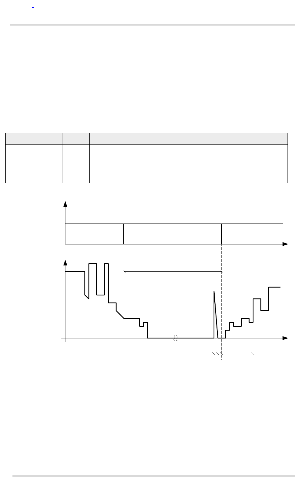
PCS3_HD_v01.000-03
Confidential / Preliminary Page 50 of 101 2013-10-21
PCS3 Hardware Interface Description
3.10 Control Signals
3.10.5
Low Current Indicator
A low current indication is optionally available over the LC_IND line. By default, low current in-
dication is disabled.
For the LC_IND signal to work as a low current indicator the feature has to be enabled by AT
command (see [1]: AT^SCFG: MEopMode/PowerMgmt/LCI).
If enabled, the LC_IND signal is high when the module is sleeping. During its sleep the module
will for the most part be slow clocked with 32kHz RTC.
Table 15: Low current indicator line
Signal I/O/P Description
LC_IND O Inactive to active high transition:
0 = High current consumption
The module draws its power via BATT+
1 = Low current consumption (only reached during SLEEP mode)
The module draws only a low current via BATT+
LC_IND
1
0
t
IBATT+
tLC
ILCpk
(typ. 150mA)
ILCmax <100mA
tLCpk<100µs
tLCru> t
300µs
Figure 23: Low current indication timing
tLC Time for the IBATT+ current consumption: ILCmax<100mA.
tLCpk Max. time duration for the inrush current peak at the end of the low current period.
tLCru When the LC_IND signal becomes inactive (low) the current ramps up to the
maximum low current value within tLCru.
ILCpk When the module turns from sleep to normal operation some internal supply
voltages will be switched on. That causes a small inrush current peak.
ILCmax During the low current period tLC the current consumption does not exceed
the ILCmax value.
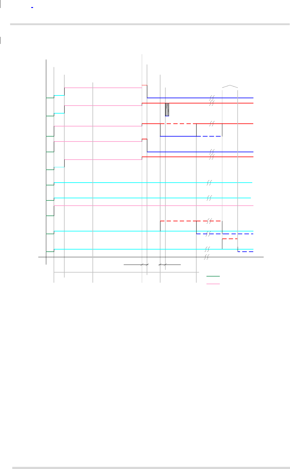
PCS3_HD_v01.000-03
Confidential / Preliminary Page 51 of 101 2013-10-21
PCS3 Hardware Interface Description
3.10 Control Signals
SDPORT=4
0
ms
appr.
34ms
(depends
on
BATT+
capacitors
appr.
1.5s
appr.
4.0s...4.5s
3.10.6
RING0 (ASC0), WAKEUP and LCI_IND Startup Behavior
Table 24 shows the startup behavior of the control lines described in the above sections.
Power startup undefined ASC0 set up (by firmware)
1st init (power on reset)
2nd init (startup phase)
ASC0 ready (by firmware)
URC Wake up signalling
Firmware start
„SYSSTART“
Sleep mode
CTS0
RXD0
RING0
1)
1) „keep“
DSR0
DCD0
TXD0
RTS0
DTR0
WAKEUP
1) 1)
„keep“
2)
LCI_IND
0.6ms 0.6ms t
151ms
2.6ms
100ms 1)
undefined (port not supplied)
Pull up (appr. 100k)
PCS3_HD_v01.000-03
Confidential / Preliminary Page 52 of 101 2013-10-21
PCS3 Hardware Interface Description
5 Antenna Interfaces
Configuration
Wakeup State
RING0
WAKEUP
AT^SCFG="URC/Ringline",
"local"
(P)
low (active) low (PD)
"asc0"
low (active) low (PD)
"off"
high
low (PD)
"wakeup"
high
high (active)
Configuration
Wakeup Active Time
for RING0, WAKEUP
AT^SCFG=
"URC/Ringline/ActiveTime",
"0"
4.6ms-9ms
"1"
(P)
100ms
"2"
1s
"keep"
keeps active until
1st time enter sleep mode
Pull down (appr. 100k)
iven high
driven
low dashed line:
lternative funtion
1)
(P) Power up default value
2) If needed: During runtime the LCI feature has to be enabled by
AT^SCFG="MEopMode/PowerMgmt/LCI","enabled"
Figure 24: RING0 (ASC0), WAKEUP and LCI_IND startup behavior
4
Antenna Interfaces
The PCS3 only CDMA main Antenna, PCS3 didn’t have GPS fora GNSS receiver
5.1
CDMA Antenna Interface
The PCS3 CDMA antenna interface comprises a main CDMA antenna as well as an optional
CDMA Rx diversity antenna to improve signal reliability and quality1. The interface has an
impedance of 50ohm PCS3 is capable of sustaining a total mismatch at the antenna interface
without any damage, even when transmitting at maximum RF power.
The external antenna must be matched properly to achieve best performance regarding
radiation power, modulation accuracy and harmonic suppression. Matching networks are not
included on the PCS3 PCB and should be placed in the host application, if the antenna does
not
have an impedance of 50ohm
Regarding the return loss PCS3 provides the following values in the active band:
Table 16: Return loss in the active band
State of module Return loss of module Recommended return loss of application
Receive > 8dB > 12dB
Transmit not applicable > 12dB
Idle < 5dB not applicable
1.
By delivery default the optional CDMA Rx diversity antenna is configured as available for the module. To
avoid negative side effects and performance degradation it is recommended to disable the diversity an-
tenna path if
- the host application does not support a diversity antenna
- the host application includes a diversity antenna - but a network simulator is used for development and
performance tests.
Please refer to [1] for details on how to configure antenna settings.
PCS3_HD_v01.000-03
Confidential / Preliminary Page 53 of 101 2013-10-21
PCS3 Hardware Interface Description
5.1 CDMA Antenna Interface
5.1.1
Antenna Installation
The antenna is connected by soldering the antenna pads and their neighboring ground pads
directly to the application’s PCB.
1 2 3 4 5 6 7 8 9 10 11 12 13 14 15 16
P
BATT
N
BATT
M
L GND
K ANT
CDMA
J GND
H
G nc
F GND
E nc
D GND nc
C
B BATT+
_
CDMA
A BATT+
_
CDMA nc GND nc
GND
Figure 25: Antenna pads
The distance between the antenna pads and their neighboring GND pads has been optimized
for best possible impedance. To prevent mismatch, special attention should be paid to these
pads on the application’ PCB.
The wiring of the antenna connection, starting from the antenna pad to the application’s anten-
na should result in a 50 line impedance. Line width and distance to the GND plane need
to
be optimized with regard to the PCB’s layer stack. Some examples are given in Section
5.1.2.
To prevent receiver desensitization due to interferences generated by fast transients like high
speed clocks on the external application PCB, it is recommended to realize the antenna con-
nection line using embedded Stripline rather than Micro-Stripline technology. Please see Sec-
tion 5.1.2 for examples of how to design the antenna connection in order to achieve the
required 50 line impedance.
For type approval purposes, the use of a 50 coaxial antenna connector (U.FL-R-SMT) might
be necessary. In this case the U.FL-R-SMT connector should be placed as close as possible
to PCS3‘s antenna pad.
PCS3_HD_v01.000-03
Confidential / Preliminary Page 54 of 101 2013-10-21
PCS3 Hardware Interface Description
5.1 CDMA Antenna Interface
5.1.2
RF Line Routing Design
5.1.2.1
Line Arrangement Examples
Several dedicated tools are available to calculate line arrangements for specific applications
and PCB materials - for example from http://www.polarinstruments.com/ (commercial software)
or from http://web.awrcorp.com/Usa/Products/Optional-Products/TX-Line/ (free software).
Coated coplanar strips with ground
This section gives two line arrangement examples for differential coated coplanar strip with
ground
Figure 26: coatedcoplanarstripwithground
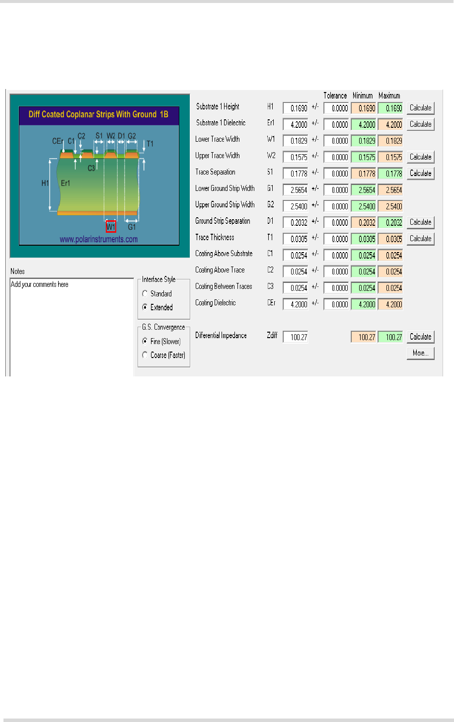
PCS3_HD_v01.000-03
Confidential / Preliminary Page 55 of 101 2013-10-21
PCS3 Hardware Interface Description
5.1 CDMA Antenna Interface
Differentialcoatedcoplanarstripswithground
This section gives two line arrangement examples for differential coated coplanar strip with
ground
Figure 27: differentialcoatedcoplanarstripwithground
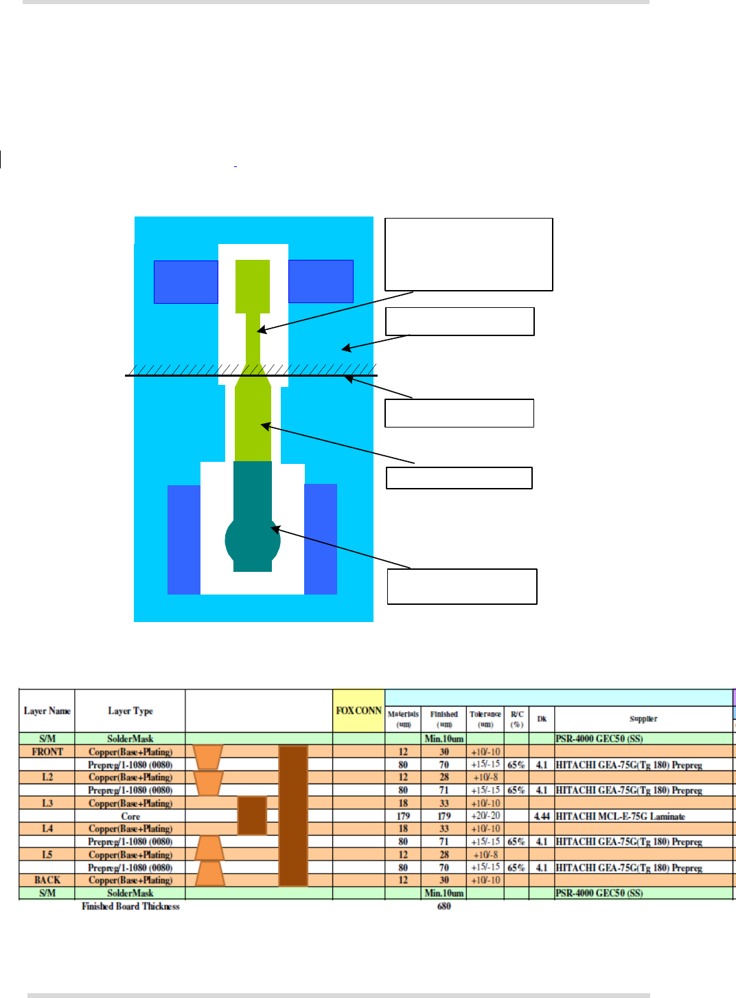
PCS3_HD_v01.000-03
Confidential / Preliminary Page 56 of 101 2013-10-21
PCS3 Hardware Interface Description
5.1 CDMA Antenna Interface
5.1.2.2
Routing Example
Interface to RF Connector
Figure 28 shows a sample connection of a module‘s antenna pad at the bottom layer of the
module PCB with an application PCB‘s coaxial antenna connector. Line impedance depends
on line width, but also on other PCB characteristics like dielectric, height and layer gap. The
sample stripline width of 0.33mm is recommended for an application with a PCB layer stack
resembling the one of the PCS3 evaluation board shown in Figure 29. For different layer stacks
the stripline width will have to be adapted accordingly.
G N D
e.g.
ANT_
MAIN
G N D
Stripline (50Ohm) on top layer
of evaluation board from
antenna pad to module edge
Width = 0.33 mm
Ground connection
Edge of module PCB
50Ohm micro stripline
G N D G N D
E.g., U.FL antenna
connector
Figure 28: Routing to application‘s RF connector
Figure 29: PCS3 evaluation board layer table

PCS3_HD_v01.000-03
Confidential / Preliminary Page 57 of 101 2013-10-21
PCS3 Hardware Interface Description
6 Electrical, Reliability and Radio Characteristics
6
Electrical, Reliability and Radio Characteristics
6.1
Absolute Maximum Ratings
The absolute maximum ratings stated in Table 17 are stress ratings under any conditions.
Stresses beyond any of these limits will cause permanent damage to PCS3.
Table 17: Absolute maximum ratings
Parameter Min Max Unit
Supply voltage BATT+ -0.5 +4.2 V
Voltage at all digital lines in POWER DOWN mode -0.3 +0.3 V
Voltage at digital lines in normal operation -0.3 +2.1 V
Voltage at analog audio lines in normal operation
(VMIC=on) -0.3 +1.8 V
Voltage at analog audio lines during audio off mode
(VMIC=off) -0.3 +0.3 V
VDDLP input voltage -0.3 +3.5 V
Microphone supply (VMIC) maximum current to GND 3 mA
VEXT maximum current shorted to GND -300 mA
VUSB_IN, USB_DN, USB_DP -0.3 5.75 V
Voltage at PWR_IND line -0.5 5.5 V
PWR_IND input current if PWR_IND= low 2 mA
Voltage at following signals:
IGT, EMERG_OFF -0.5 VBATT+ V

PCS3_HD_v01.000-03
Confidential / Preliminary Page 58 of 101 2013-10-21
PCS3 Hardware Interface Description
6.2 Operating Temperatures
6.2
Operating Temperatures
Table 18: Board temperature
Parameter Min Typ Max Unit
Operating temperature range -30 +25 +85 °C
Restricted temperature range1 -40 +95 °C
Automatic shutdown2
Temperature measured on PCS3 board <-40 ---
>+95
°C
1.
Restricted operation allows normal mode speech calls or data transmission for limited time until au-
tomatic thermal shutdown takes effect. Within the restricted temperature range (outside the operating
temperature range) the specified electrical characteristics may be in- or decreased.
2.
Due to temperature measurement uncertainty, a tolerance on the stated shutdown thresholds may occur.
The possible deviation is in the range of ± 2°C at the overtemperature and undertemperature limit.
6.3
Storage Conditions
The conditions stated below are only valid for modules in their original packed state in weather
protected, non-temperature-controlled storage locations. Normal storage time under these
conditions is 12 months maximum.
Table 19: Storage conditions
Type Condition Unit Reference
Air temperature: Low
High -25
+40 °C IPC/JEDEC J-STD-033A
Humidity relative: Low
High 10
90 at 40°C % IPC/JEDEC J-STD-033A
Air pressure: Low 70 kPa IEC TR 60271-3-1: 1K4
High 106 IEC TR 60271-3-1: 1K4
Movement of surrounding air 1.0 m/s IEC TR 60271-3-1: 1K4
Water: rain, dripping, icing and
frosting Not allowed --- ---
Radiation: Solar 1120 W/m2ETS 300 019-2-1: T1.2, IEC 60068-2-2 Bb
Hea
t
600 ETS 300 019-2-1: T1.2, IEC 60068-2-2 Bb
Chemically active substances Not recom-
mended
IEC TR 60271-3-1: 1C1L
Mechanically active sub-
stances Not recom-
mended
IEC TR 60271-3-1: 1S1
Vibration sinusoidal:
1.5 mm IEC TR 60271-3-1: 1M2
Displacemen
t
Acceleration 5 m/s
2
Frequency range 2-9 9-200 Hz
Shocks:
semi-sinusoidal
ms
IEC 60068-2-27 Ea
Shock spectrum
Duration 1
Acceleration 50 m/s
2

PCS3_HD_v01.000-03
Confidential / Preliminary Page 59 of 101 2013-10-21
PCS3 Hardware Interface Description
6.4 Reliability Characteristics
6.4
Reliability Characteristics
The test conditions stated below are an extract of the complete test specifications.
Table 20: Summary of reliability test conditions
Type of test Conditions Standard
Vibration Frequency range: 10-20Hz; acceleration: 5g
Frequency range: 20-500Hz; acceleration: 20g
Duration: 20h per axis; 3 axes
DIN IEC 60068-2-61
Shock half-sinus Acceleration: 500g
Shock duration: 1msec
1 shock per axis
6 positions (± x, y and z)
DIN IEC 60068-2-27
Dry heat Temperature: +70 ±2×C
Test duration: 16h
Humidity in the test chamber: < 50%
EN 60068-2-2 Bb
ETS 300 019-2-7
Temperature
change (shock) Low temperature: -40×C ±2×C
High temperature: +85×C ±2×C
Changeover time: < 30s (dual chamber system)
Test duration: 1h
Number of repetitions: 100
DIN IEC 60068-2-14 Na
ETS 300 019-2-7
Damp heat cyclic High temperature: +55×C ±2×C
Low temperature: +25×C ±2×C
Humidity: 93% ±3%
Number of repetitions: 6
Test duration: 12h + 12h
DIN IEC 60068-2-30 Db
ETS 300 019-2-5
Cold (constant
exposure) Temperature: -40 ±2×C
Test duration: 16h DIN IEC 60068-2-1
1.
For reliability tests in the frequency range 20-500Hz the Standard’s acceleration reference value was inc-
reased to 20g.
6.5
Pad Assignment and Signal Description
The SMT application interface on the PCS3 provides connecting pads to integrate the module
into external applications. The following Table 21 lists the pads’ assignments, Figure 32 (bot-
tom view) and Figure 33 (top view) show the connecting pads’ numbering plan.
Please note that a number of connecting pads are marked as reserved for future use (rfu) or
ground (GND) and further qualified as either (dnu), (GND) or (nc):
•
Pads marked "rfu" and qualified as "dnu" (do not use) may be soldered but should not be
connected to an external application.
•
Pads marked "rfu" and qualified as "GND" (ground) are assigned to ground with PCS3 mod-
ules, but may have different assignments with future Cinterion products using the same pad
layout.
•
Pads marked "GND" and qualified as "nc" (not connected) are internally not connected with
PCS3 modules but may be soldered and arbitrarily be connected to external ground.
Because with surface mount modules the heat is transported through the solder pads to the
external application’s PCB, it is generally recommended to solder all pads.
PCS3_HD_v01.000-03
Confidential / Preliminary Page 60 of 101 2013-10-21
PCS3 Hardware Interface Description
6.5 Pad Assignment and Signal Description
Table 21: Overview: Pad assignments
Pad
No. Signal Name Pad
No. Signal Name Pad
No. Signal Name
A4 BATT+ CDMA2 E2 GND L2 GND
A5 GND E3 GND L3 GND
A6 GND E4 GND L4 GND
A7 nc E5 GND L5 nc
A8 GND E12 nc L6 nc
A9 GND E13 nc L7 nc
A10 GND E14 nc L8 nc
A11 GND E15
EPP( voice&data variant
onl
y
)
L9 nc
A12 nc E16
EPN( voice&data variant
only) L10 nc
13 GND F1 GND L11 nc
B3 BATT+ CDMA F2 GND L12 nc
B4 GND F3 GND L13 nc
B5 GND F4 GND L14 CCRST
(
o
p
tion CSIM
)
B6 GND F13 nc L15 CCCLK
(
o
p
tion CSIM
)
B7 GND F14 I2CCLK L16 IGT
B8 GND F15 I2CDAT M2 GND
B9 GND F16 GPIO10 M3 GND
B10 GND G1 GND M4 PWR IND
B11 GND G2 GND M5 VEXT
B12 GND G3 GND M6 GND
B13 GND G4 nc M7
PCM
_
IN( voice&data
variant onl
y
)
B14 STATUS G13 nc M8
PCM
_
CLK( voice&data
variant only)
C2 GND G14 GPIO7 M9
PCM
_
FSC( voice&data
variant only)
C3 GND G15 GPIO8 M10
PCM
_
OUT( voice&data
variant only)
C4 GND G16 GPIO9 M11 nc
C5 GND H1 GND M12 ADC2 IN
C6 GND H2 GND M13 ADC1 IN
C7 GND H3 GND M14 CCIN
(
o
p
tion CSIM
)
C8 GND H4 GND M15 VDDLP
C9 GND H13 nc N3 nc
C10 GND H14 GPIO4 N4 nc
C11 GND H15 GPIO5 N5 VUSB IN
C12 nc H16 GPIO6 N6 nc
C13 nc J1 GND N7 nc
C14 VMIC J2 GND N8 CTS0
C15 AGND J3 GND N9 DCD0
D1 GND J4 GND N10 RTS0
D2 GND J13 nc N11 GND
D3 GND J14 GPIO1 N12 nc
D4 GND J15 GPIO2 N13 BATT+
D5 nc J16 GPIO3 N14 EMERG OFF
D6 GND K1 ANT CDMA P4 USB DP
D7 GND K2 GND P5 USB DN
D8 GND K3 GND P6 nc
D9 GND K4 GND P7 nc
D10 GND K5 GND P8 DTR0
D11 GND K12 nc P9 DSR0
D12 GND K13 nc P10 RING0
D13 GND K14 CCIO
(
o
p
tion CSIM
)
P11 RXD0
D14 GND K15 CCVCC
(
o
p
tion CSIM
)
P12 TXD0
D15 MICP K16 nc P13 BATT+
D16 MICN L1 GND
E1 nc
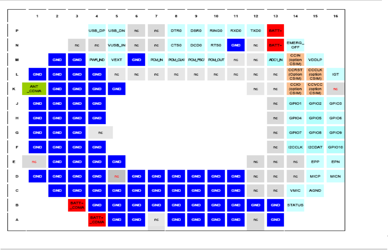
6.5 Pad Assignment and Signal Description
PCS3_HD_v01.000
Confidential / Preliminary Page 61 of 101 2013-10-21
PCS3 Hardware Interface Description
Figure 32: PCS3 bottom view: Pad assignments

PCS3 Hardware Interface Description
6.5 Pad Assignment and Signal Description
PCS3_HD_v01.000
Confidential / Preliminary Page 68 of 101 2013-10-21
Please note that the reference voltages listed in Table 22 are the values measured directly on
the PCS3 module. They do not apply to the accessories connected.
Table 22: Signal description
Function Signal name IO Signal form and level Comment
Power
supply
BATT+_CDMA
BATT+_CDMA
I VImax = 4.2V
VInorm = 3.8V
VImin = 3.3V during Tx burst on board
Imax 800mA, during Tx burst
Lines of BATT+ and GND
must be connected in paral-
lel for supply purposes
because higher peak cur-
rents may occur.
Minimum voltage must not
fall below 3.3V including
drop, ripple, spikes.
BATT+ I
VImax = 4.2V
VInorm = 3.8V
VImin = 3.3V during Tx burst on board
Imax = 250mA
Power
supply
GND Ground Application Ground
External
supply
voltage
VEXT O CLmax = 1µF
High power mode:
VO = 1.80V +1% -5%
IOmax = -50mA
Power save mode:
VO = 1.80V +2% -5%
IOmax = -10mA
VEXT may be used for
application circuits. Not
available in Power down
mode.
If unused keep line open
and enable power save
mode via AT^SCFG=
"MEopMode/PowerMgmt/
VEXT", "low" (see [1])
The external digital logic
must not cause any spikes
or glitches on voltage
VEXT.
Ignition IGT I
RPU 160k , CI
1nF
VOHmax=1.85V
VIHmax =2.2V
VIHmin = 1.17V
VILmax = 300mV
Low impulse width > 100ms
This signal switches the
module ON.
It is recommended to drive
this line low by an open
drain or open collector
driver connected to GND.
Emer-
gency Off EMERG_OFF I RPU 160k , CI
1nF
VOHmax=1.85V
VIHmax =2.2V
VIHmin = 1.17V
VILmax = 300mV
~~| |~~ low impulse width > 40ms
It is recommended to drive
this line low by an open
drain or open collector
driver connected to GND.
If unused keep line open.

PCS3 Hardware Interface Description
6.5 Pad Assignment and Signal Description
PCS3_HD_v01.000
Confidential / Preliminary Page 69 of 101 2013-10-21
Table 22: Signal description
Function Signal name IO Signal form and level Comment
RTC
Back up VDDLP O
VOmax = 3.20V while BATT+ =>3.3V
RI = 1.8k
If unused keep line open.
To employ the SMPL fea-
ture the VDDLP line has to
supplied for at least 2 sec-
onds after a possible power
loss (e.g., by connecting a
10µF capacitor). See also
Section 3.3.6.
I VI = 1.5V…3.25V at Imax= 10µA while
BATT+ = 0V
Connectiv-
ity Status STATUS O
VOLmax = 0.45V at I = 2mA
VOHmin = 1.35V at I = -2mA
VOHmax = 1.85V
Status signalling e.g. with
ext. LED circuit
Serial
Modem
Interface
ASC0
RXD0 O
VOLmax = 0.45V at I = 2mA
VOHmin = 1.35V at I = -2mA
VOHmax = 1.85V
If unused keep line open.
CTS0 O
DSR0 O
DCD0 O
RING0 O
TXD0 I
VILmax = 0.6V at 30µA
VIHmin = 1.20V at -30µA
VIHmax = 2V
RTS0 I
DTR0 I
Analog
Audio
interface
VMIC O
VOtyp = 1.8V
Imax = 3 mA Microphone supply for cus-
tomer feeding circuits.
If unused keep line open.
EPP O Differential,
Minimum load resistance 32
typ. 5.0Vpp at no load
PCM level = +3dBm0, 1.02kHz sine
wave
Balanced output for ear-
phone or balance output for
line out. See also Section
6.7.4.
If unused keep line open.
EPN O
MICP I
ZItyp = 94k @ 0dB
gain
ZItyp = 5.8k @
30dB gain
Vinmax = 2.57Vpp
(for 3dBm0 @ 0dB gain)
Balanced differential micro-
phone with external feeding
circuit (using VMIC and
AGND) or balanced differ-
ential line input. See also
Section 6.7.4.
Use coupling capacitors.
If unused keep lines open.
MICN I
AGND Analog ground GND level for external
audio circuits

PCS3 Hardware Interface Description
6.5 Pad Assignment and Signal Description
PCS3_HD_v01.000
Confidential / Preliminary Page 70 of 101 2013-10-21
Table 22: Signal description
Function Signal name IO Signal form and level Comment
Pulse Code
Modulation
(PCM)
PCM_IN I
VILmax = 0.6V at 30µA
VIHmin = 1.20V at -30µA
VIHmax = 2V
VOLmax = 0.45V at I = 2mA
VOHmin = 1.35V at I = -2mA
VOHmax = 1.85V
In Master mode PCM_FSC
and PCM_CLK are output
signals1.
In Slave mode PCM_FSC
and PCM_CLK are input
signals. See also Section
3.9.1.
If unused keep line open.
PCM_CLK I/O
PCM_FSC I/O
PCM_OUT O
Inter IC
interface
(I2C)
I2CDAT O VOLmax = 0.45V at I = 2mA
VOHmin = 1.35V at I = -2mA
VOHmax = 1.85V
I2CCLK O
Power
Indicator PWR_IND O
VIHmax = 5.5V
VOLmax = 0.4V at Imax = 2mA
PWR_IND (Power Indica-
tor) notifies the module’s
on/off state.
PWR_IND is an open col-
lector that needs to be con-
nected to an external pull-
up resistor. Low state of the
open collector indicates
that the module is on. Vice
versa, high level notifies the
power-down mode.
Therefore, the signal may
be used to enable external
voltage regulators which
supply an external logic for
communication with the
module, e.g. level convert-
ers.
USB VUSB_IN I
VINmin = 3.0V
VINmax = 5.25V
Active current
IItyp = 105µA (max 130µA)
Suspend current
IItyp = 135µA (max 200µA)
If the USB interface is not
used please connect this
line to GND.
USB_DN I/O
All electrical characteristics according
to USB Implementers’ Forum, USB
2.0 Full Speed Specification.
If lines are unused keep
lines open.
USB only support Full
Speed mode
operation
requires a differential
impedance of 90ohm
USB_DP I/O
Host
wakeup
WAKEUP O
VOLmax = 0.45V at I = 2mA
VOHmin = 1.35V at I = -2mA
VOHmax = 1.85V
Can be used as a host
wakeup line similar to
RING0 (see Section
3.10.4)1.

PCS3 Hardware Interface Description
6.5 Pad Assignment and Signal Description
PCS3_HD_v01.000
Confidential / Preliminary Page 71 of 101 2013-10-21
Table 22: Signal description
Function Signal name IO Signal form and level Comment
Low
Current
Indication
LC_IND O
VOLmax = 0.45V at I = 2mA
VOHmin = 1.35V at I = -2mA
VOHmax = 1.85V
If the function is enabled
(see Section 3.10.5)1.
I VIHmax = 2V
RPD= appr. 100kOhm
If the function is disabled
(see Section 3.10.5)1.
1.
Signal state if not configured: I, PD (appr. 100k)

PCS3_HD_v01.000
Confidential / Preliminary Page 72 of 101 2013-10-21
PCS3 Hardware Interface Description
6.6 Power Supply Ratings
6.6
Power Supply Ratings
Table 23: Power supply ratings
Description Conditions Min Typ Max Unit
BATT+ Supply voltage Directly measured at Module.
Voltage must stay within the min/max values,
including voltage drop, ripple, spikes
3.3 3.8 4.2 V
Maximum allowed
voltage drop dur-
ing transmit burst
Normal condition, power control level for
Pout max
400 mV
Voltage ripple Normal condition, power control level for
Pout max
@ f <= 250 kHz
@ f > 250 kHz
20
16
mVpp
mVpp
IVDDLP
@ 3V OFF State supply
current RTC backup @ BATT+ = 0V 4.0 µA
IBATT+ 1 OFF State supply
current POWER DOWN 39
µA
Average CDMA
supply current
SLEEP2 (USB Suspend or Disconnected
and no communication via ASC0) @ SCI=0
8 mA
SLEEP2 (USB Suspend or Disconnected
and no communication via ASC0) @ SCI=2
8 mA
SLEEP2 (USB Suspend or Disconnected
and no communication via ASC0) @ SCI=7
8 mA
1xRTT Data transfer BC0 @ +24dBm 450 mA
1xRTT Data transfer BC1 @ +24dBm 500 mA
1xRTT Data transfer BC10 @ +24dBm 460 mA
IVUSB_IN USB suspend and active ratings are mentioned in Table 22: VUSB_IN.
1.
With an impedance of ZLOAD=50Ohm at the antenna connector.
2.
Average time for SLEEP mode: 5min

PCS3_HD_v01.000
Confidential / Preliminary Page 73 of 101 2013-10-21
PCS3 Hardware Interface Description
6.7 Electrical Characteristics of the Voiceband Part
6.7
Electrical Characteristics of the Voiceband Part
6.7.1
Setting Audio Parameters by AT Commands
Audio mode 1 is the basic audio mode optimized for the Votronic reference handset (see Sec-
tion 10.1). The default parameters are determined for type approval and are not adjustable with
AT commands.
The audio modes 2 to 8 can be temporarily adjusted according to the AT command parameters
listed in the table below. The audio parameters are set with the AT commands AT^SNFI as well
as AT^SNFO and stored volatile for the current audio mode (see [1]). For a model of how the
parameters influence the audio signal path see Section 6.7.2.
Table 24: Audio parameters adjustable by AT command
Parameter Influence to Range Gain range Calculation
AT^SNFI=
micAmp1 MICP/MICN second analog ampli-
fier gain of before ADC 0,1 0 or 24dB
micTxVol Digital gain of input signal after ADC 0,
1...65535 Mute,
-84...+12dB 20 * log (micTxVol/
16384)
AT^SNFO=
cdcRxGain Analog gain of output signal after
summation of sidetone 0...63 -57...+6dB 1dB steps
rxVol Digital Volume of output signal after
speech decoder, before summation
of sidetone and DAC
0,
1…41 Mute,
-48...+12dB 1.5dB steps
stGain Digital attenuation of sidetone 0,
1...65535 Mute,
-96...0dB 20 * log (stGain/
16384) -12
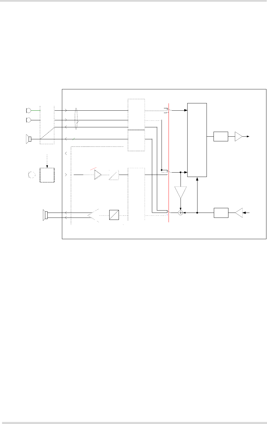
PCS3_HD_v01.000
Confidential / Preliminary Page 74 of 101 2013-10-21
PCS3 Hardware Interface Description
6.7 Electrical Characteristics of the Voiceband Part
Echo
canceller,
Noise
suppresson
with
one or two
Micro-
phones
Filter
flat gain=0dB
6.7.2
Audio Programming Model
The audio programming model shows how the signal path can be influenced by varying AT
command parameters: AT^SNFI allows to set the parameters <micAmp1>, and<mic TxVol>,
whereas the parameters <cdcRxGain>, <stGain> and <rxVol> can be adjusted
with AT^SNFO.
For more information on the AT commands and parameters see Section 6.7.1
and [1].
If the digital audio interface (PCM) is selected, the parameters <micAmp1>, and <cdcRxGain>
have no influence; because they are not involved in the signal paths.(PCS3 didn’t support I2S)
Application
Digital logical channels:
gain=0dB
<io>
gain=0dB
Aux MIC
Main MIC
Speaker
Codec
I
2
S right channel
I
2
S left channel / PCM mono
4 PCM mono
I
2
S left channel
4
PCM /
I
2
S
Interface
I
2
S
Interface
1
3
2
<micTxVol>
Speech
coder
VMIC
Codec
MIC
Microphon
e
feeding
EP
<micAmp1>
A
D
<cdcRxGain>
D
gain=0dB
PCM
1
3
2
<stGain>
3
2
<rxVol>
Filter
Speech
coder
32 Ohms
A
flat gain=0dB
Module
Red: Audio mode parameters adjustable by AT commands
Orange: Selectable Audio Mode Parameter - on request adjustable by Cinterion
Figure 34: Audio programming model

6.7 Elec
t
rical Charac
t
eristics of
t
he Voiceband Par
t
PCS3_HD_v01.000
Confidential / Preliminary Page 75 of 101 2013-10-21
PCS3 Hardware Interface Description
6.7.3
Characteristics of Audio Modes
The electrical characteristics of the voiceband part depend on the current audio mode set with AT command. All values are noted for default gains, e.g.
the default parameters are left unchanged.
Table 25: Voiceband characteristics
Audio mode no.
AT^SNFS= 11 2 3 4 5 6
Name Default Handset Router User Handset Headset Speaker phone Transparent
Purpose DSB with
Votronic handset Analog phone
interface
Mono Headset Handheld
speakerphone
Direct access
to speech
coder
TX-Filters Adjusted Flat Adjusted Flat Flat Flat
RX-Filters Adjusted to fit
artificial ear type
3.2 low leakage
Flat Adjusted to fit
artificial ear
type
3.2 low
leakage
800Hz 800Hz Flat
Default SNFI Parameters
<micAmp1>
<txVol>
0 (0dB)
0x23FD (-5dB)
0 (0dB)
0x4000 (0dB)
0 (0dB)
0x23FD (-5dB)
1 (24dB)
0x4000 (0dB)
1 (24dB)
0xB461(9dB)
0 (0dB)
0x4000 (0dB)
Default SNFO Parameters
<cdcRxGain>
<rxVol>
<stGain>
0x2861 (-4dB)
33 (0dB)
0x261F (-16.5dB)
0x2000 (-6dB)
33 (0dB)
0x0000 (mute)
0x2861 (-4dB)
33 (0dB)
0x261F (-16.5dB)
0x2000 (-6dB)
33 (0dB)
0x1000 (-24dB)
0x6570 (4dB)
33 (0dB)
0x0000 (mute)
0x4000 (0dB)
33 (0dB)
0x0000 (mute)
Echo canceller mode VOC_EC_ESEC VOC_EC_ESEC VOC_EC_ESEC VOC_EC_HEADSET VOC_EC_SPEAKER VOC_EC_OFF
Noise Supersession VOC_NS_ON VOC_NS_OFF VOC_NS_ON VOC_NS_ON VOC_NS_ON VOC_NS_FF
Tx codec gain 0x4000 (0dB) 0x4000 (0dB) 0x4000 (0dB) 0x4000 (0dB) 0x4000 (0dB) 0x4000 (0dB)

6.7 Elec
t
rical Charac
t
eristics of
t
he Voiceband Par
t
PCS3_HD_v01.000
Confidential / Preliminary Page 76 of 101 2013-10-21
PCS3 Hardware Interface Description
Table 25: Voiceband characteristics
Audio mode no.
AT^SNFS= 11 2 3 4 5 6
MIC input signal for
0dBm0, 2
f = 1024 Hz 15mV 650mV 15mV 12mV 5mV 420mV
EP output signal in mV
rms. @ 0dBm0,
1024 Hz, no load (default
gain) /
@ 3.14 dBm0
465mV 2.1Vpp
512mV 2.1Vpp
465mV 2.1Vpp
370mV 1.6Vpp
1485mV 5.7Vpp
1290mV 5.5Vpp
Sidetone gain at default
settings
-16.5dB
0dB
-16.5dB
-24dB
0dB
0dB
Digital audio characteristics (PCM)
Uplink gain at 1024Hz 14602(-1dBm) 16384(0dBm) 14602(-1dBm) 16384(0dBm) 16384(0dBm) 16384(0dBm)
Downlink gain at 1024Hz 25 33 25 32 32 33
Sidetone gain 5514(-21.5dBm) 0 5514(-21.5dBm) 12288(-15dBm) 0 0
1.
Fixed audio mode. Values cannot be adapted.
2.
All values measured before the noise reduction attenuates the sine wave after a few seconds.
n.a. = not applicable
Note: With regard to acoustic shock, the cellular application must be designed to avoid sending false AT commands that might increase amplification,
e.g.
for a highly sensitive earpiece. A protection circuit should be implemented in the cellular application.

PCS3 Hardware Interface Description
6.7 Electrical Characteristics of the Voiceband Part
PCS3_HD_v01.000
Confidential / Preliminary Page 77 of 101 2013-10-21
6.7.4
Voiceband Receive Path
Test conditions:
•
The values specified below were tested to 1024Hz using AT^SNFO=57,33,0 in audio mode
6 during a voice call unless otherwise stated.
Table 26: Voiceband receive path
Parameter Min Typ Max Unit Test condition / remark
Maximum differential output voltage 4.5 V 32 ,
(peak
t
o peak) 5.0 V No load,
EPP to EPN @ 3.14dBm0 (Full Scale)
Nominal differential output voltage 3.1 V 32 ,
(peak
t
o peak) 3.4 V No load,
EPP to EPN @ 0dBm0 (Nominal level)
Output bias voltage 1.5 V From EPP or EPN to GND
Differential output load resistance 16
6.7.5
Voiceband Transmit Path
Test conditions:
•
The values specified below were tested to 1024Hz using AT^SNFI=0,16,16384 in audio
mode 6 during a voice call unless otherwise stated.
Table 27: Voiceband transmit path
Parameter Min Typ Max Unit Test condition / Remark
Full scale input voltage (peak to
peak) for 3.14dBm0
MICP to MICN
2.57 V Balanced
Nominal input voltage (rms) for
0dBm0
MICP to MICN
0.64 V Balanced
Input amplifier 1 gain (micAmp1) 0 24 dB Set with AT^SNFI
Fine scaling by DSP (micTxVol) -84 12 dB Set with AT^SNFI
Microphone supply voltage VMIC 1.8 V No load
Microphone supply voltage VMIC 1.8 V @ 3mA

PCS3_HD_v01.000
Confidential / Preliminary Page 78 of 101 2013-10-21
6.8
RF Antenna Interface Characteristics
Table 28: RF Antenna interface CDMA
Parameter Conditions Min. Typical Max. Unit
CDMA connectivity BC0, BC1,BC10
Receiver Input Sensitivity @ CDMA BC0
-108.5
-110
dBm
ARP 1xRTT
CDMA BC1
-107.5
-108.5
dBm
1xRTT
CDMA BC10
1xRTT
-108.5
-110
dBm
RF Power@ ARP with CDMA BC0 +21
+21 +24
+24 +25
+25
dBm
50Oh
m
Loa
d
1xRTT
CDMA BC1
1xRTT +21
+21 +24
+24 +25
+25
dBm
CDMA BC10 +21
+21 +24
+24 +25
+25
dBm

PCS3_HD_v01.000
Confidential / Preliminary Page 79 of 101 2013-10-21
PCS3 Hardware Interface Description
6.10 Electrostatic Discharge
6.9
Electrostatic Discharge
The module is not protected against Electrostatic Discharge (ESD) in general. Consequently,
it is subject to ESD handling precautions that typically apply to ESD sensitive components.
Proper ESD handling and packaging procedures must be applied throughout the processing,
handling and operation of any application that incorporates a PCS3 module.
Special ESD protection provided on PCS3:
All antenna interfaces: Inductor/capacitor
BATT+: Inductor/capacitor
The remaining interfaces of PCS3 are not accessible to the user of the final product (since they
are installed within the device) and are therefore only protected according to the JEDEC
JESD22-A114D requirements.
PCS3 has been tested according to the following standards. Electrostatic values can be gath-
ered from the following table.
Table 31: Electrostatic values
Specification / Requirements Contact discharge Air discharge
JEDEC JESD22-A114D
All SMT interfaces ± 1kV Human Body Model n.a.
ETSI EN 301 489-1/7
All antenna interfaces
(CDMA/GNSS) ± 4kV ± 8kV
BATT+ ± 4kV ± 8kV
Note: Please note that the values may vary with the individual application design. For example,
it matters whether or not the application platform is grounded over external devices like a com-
puter or other equipment, such as the Cinterion Wireless Modules reference application de-
scribed in Chapter 9.
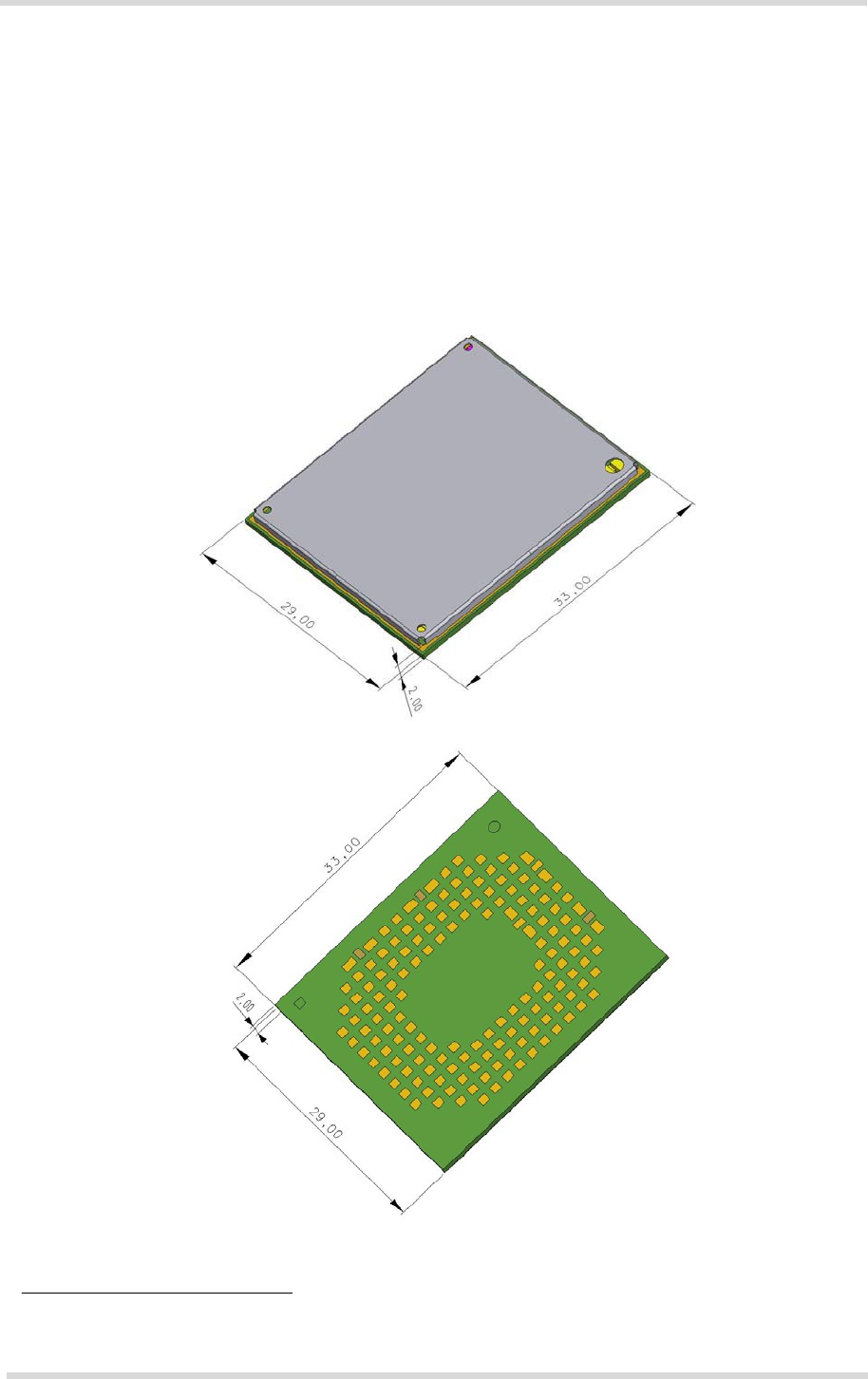
PCS3_HD_v01.000
Confidential / Preliminary Page 80 of 101 2013-10-21
PCS3 Hardware Interface Description
7 Mechanics, Mounting and Packaging
7
Mechanics, Mounting and Packaging
7.1
Mechanical Dimensions of PCS3
Figure 35 shows a 3D view1 of PCS3 and provides an overview of the board's mechanical di-
mensions. For further details see Figure 36.
Length: 33mm
Width: 29mm
Height: 2mm
Top view
Bottom view
Figure 35: PCS3 – top and bottom view
1.
The coloring of the 3D view does not reflect the module’s real color.
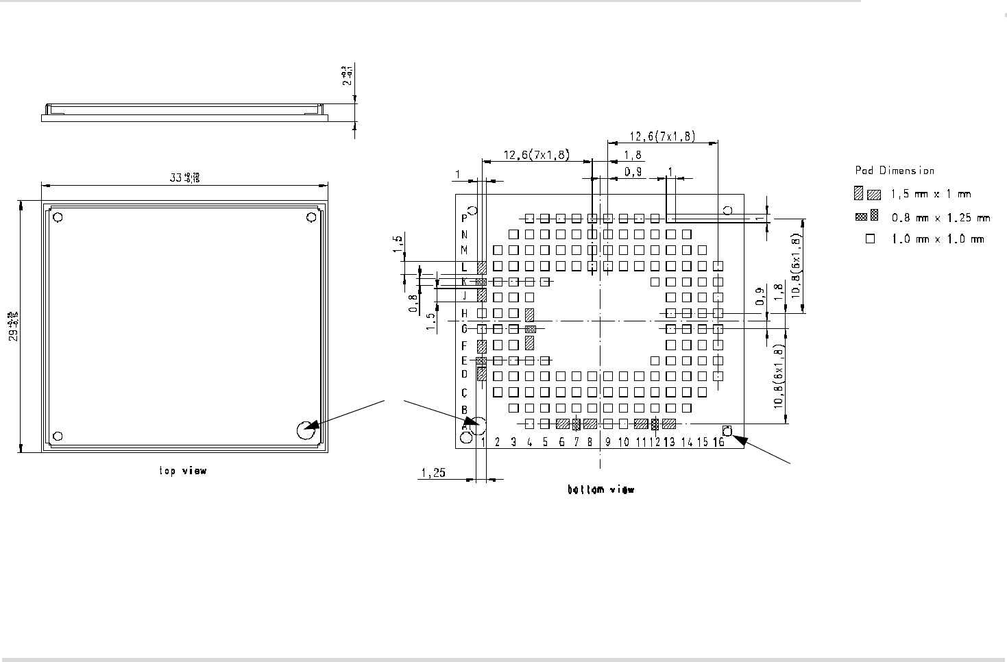
PCS3 Hardware Interface Description
7.1 Mechanical Dimensions of PCS3
Position marker
Internal use;
Not to be soldered
Figure 36: Dimensions of PCS3 (all dimensions in mm)
PCS3_HD_v01.000 Page 82 of 101
2013-10-21
Confidential / Preliminary
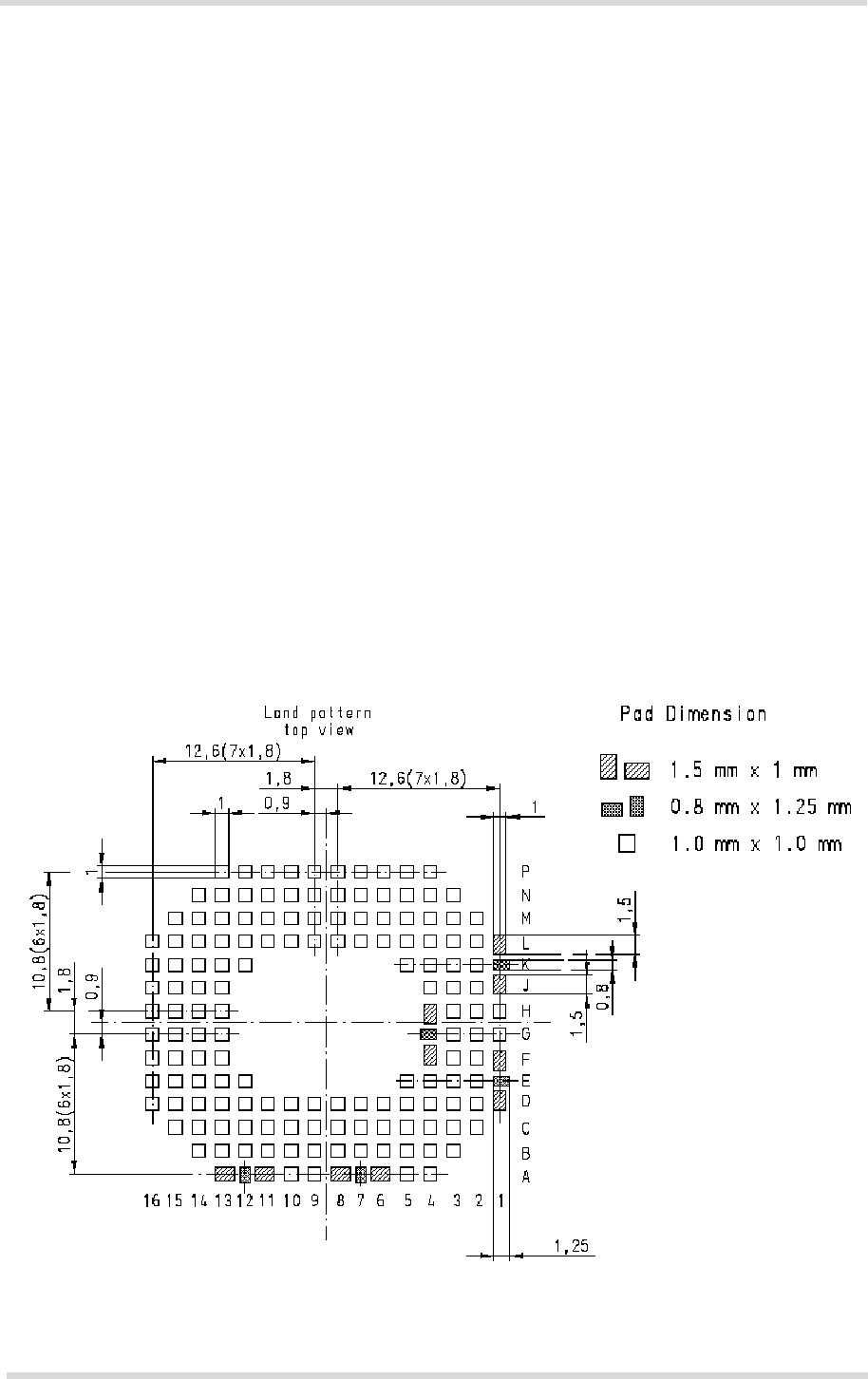
PCS3 Hardware Interface Description
7.2 Mounting PCS3 onto the Application Platform
PCS3_HD_v01.000
Confidential / Preliminary Page 83 of 101 2013-10-21
7.2
Mounting PCS3 onto the Application Platform
This section describes how to mount PCS3 onto the PCBs (=printed circuit boards), including
land pattern and stencil design, board-level characterization, soldering conditions, durability
and mechanical handling. For more information on issues related to SMT module integration
see also [4].
Note: All SMT module pads need to be soldered to the application’s PCB. Not only must all sup-
ply pads and signals be connected appropriately, but all pads denoted as “Do not use“ will also
have to be soldered (but not electrically connected) in order to ensure the best possible me-
chanical stability.
7.2.1
SMT PCB Assembly
7.2.1.1
Land Pattern and Stencil
The land pattern and stencil design as shown below is based on Cinterion characterizations for
lead-free solder paste on a four-layer test PCB and a 110 respectively 150 micron-thick stencil.
The land pattern given in Figure 37 reflects the module‘s pad layout, including signal pads and
ground pads (for pad assignment see Section 6.5). Besides these pads there are ground areas
on the module's bottom side that must not be soldered, e.g., the position marker. To prevent
short circuits, it has to be ensured that there are no wires on the external application side that
may connect to these module ground areas.
Figure 37: Land pattern (top view)
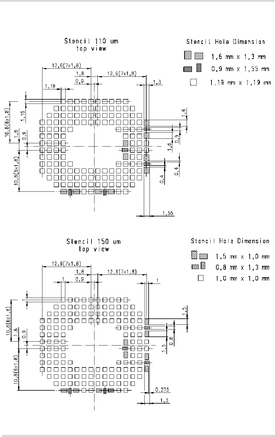
PCS3 Hardware Interface Description
7.2 Mounting PCS3 onto the Application Platform
PCS3_HD_v01.000
Confidential / Preliminary Page 84 of 101 2013-10-21
The stencil design illustrated in Figure 38 and Figure 39 is recommended by Cinterion as a re-
sult of extensive tests with Cinterion Daisy Chain modules.
Figure 38: Recommended design for 110 micron thick stencil (top view)
Figure 39: Recommended design for 150 micron thick stencil (top view)

PCS3 Hardware Interface Description
7.2 Mounting PCS3 onto the Application Platform
PCS3_HD_v01.000
Confidential / Preliminary Page 85 of 101 2013-10-21
7.2.1.2
Board Level Characterization
Board level characterization issues should also be taken into account if devising an SMT pro-
cess.
Characterization tests should attempt to optimize the SMT process with regard to board level
reliability. This can be done by performing the following physical tests on sample boards: Peel
test, bend test, tensile pull test, drop shock test and temperature cycling. Sample surface
mount checks are described in [4].
It is recommended to characterize land patterns before an actual PCB production, taking
individual processes, materials, equipment, stencil design, and reflow profile into account. For
land
and stencil pattern design recommendations see also Section 7.2.1.1. Optimizing the
solder
stencil pattern design and print process is necessary to ensure print uniformity, to
decrease sol-
der voids, and to increase board level reliability.
Daisy chain modules for SMT characterization are available on request. For details refer to [4].
Generally, solder paste manufacturer recommendations for screen printing process
parameters and reflow profile conditions should be followed. Maximum ratings are described in
Section
7.2.3.
7.2.2
Moisture Sensitivity Level
PCS3 comprises components that are susceptible to damage induced by absorbed moisture.
Cinterion’s PCS3 module complies with the latest revision of the IPC/JEDEC J-STD-020
standard for moisture sensitive surface mount devices and is classified as MSL 4.
For additional MSL (=moisture sensitivity level) related information see Section 7.2.4 and Sec-
tion 7.3.2.
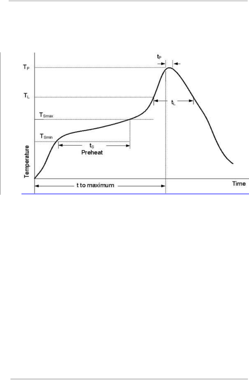
PCS3 Hardware Interface Description
7.2 Mounting PCS3 onto the Application Platform
PCS3_HD_v01.000
Confidential / Preliminary Page 86 of 101 2013-10-21
7.2.3
Soldering Conditions and Temperature
7.2.3.1
Reflow Profile
Figure 40: Reflow Profile

PCS3 Hardware Interface Description
7.2 Mounting PCS3 onto the Application Platform
PCS3_HD_v01.000
Confidential / Preliminary Page 87 of 101 2013-10-21
Table 31: Reflow temperature ratings
Profile Feature Pb-Free Assembly
Preheat & Soak
Temperature Minimum (TSmin)
Temperature Maximum (TSmax)
Time (tSmin to tSmax) (tS)
150°C
200°C
60-120 seconds
Average ramp up rate (TSmax to TP) 3K/second max.
Liquidous temperature (TL)
Time at liquidous (tL) 217°C
60-90 seconds
Peak package body temperature (TP) 245°C +0/-5°C
Time (tP) within 5 °C of the peak package body
temperature (TP) 30 seconds max.
Average ramp-down rate (TP to TSmax) 6 K/second max.
Time 25°C to maximum temperature 8 minutes max.
7.2.3.2
Maximum Temperature and Duration
The following limits are recommended for the SMT board-level soldering process to attach the
module:
•
A maximum module temperature of 245°C. This specifies the temperature as measured at
the module’s top side.
•
A maximum duration of 30 seconds at this temperature.
Please note that while the solder paste manufacturers' recommendations for best temperature
and duration for solder reflow should generally be followed, the limits listed above must not be
exceeded.
PCS3 is specified for one soldering cycle only. Once PCS3 is removed from the application,
the
module will very likely be destroyed and cannot be soldered onto another application.

PCS3 Hardware Interface Description
7.2 Mounting PCS3 onto the Application Platform
PCS3_HD_v01.000
Confidential / Preliminary Page 88 of 101 2013-10-21
7.2.4
Durability and Mechanical Handling
7.2.4.1
Storage Life
PCS3 modules, as delivered in tape and reel carriers, must be stored in sealed, moisture barrier
anti-static bags. The shelf life in a sealed moisture bag is an estimated 12 month. However, such
a life span requires a non-condensing atmospheric environment, ambient temperatures below
40°C and a relative humidity below 90%. Additional storage conditions are listed in Table 24.
7.2.4.2
Processing Life
PCS3 must be soldered to an application within 72 hours after opening the MBB (=moisture
barrier bag) it was stored in.
As specified in the IPC/JEDEC J-STD-033 Standard, the manufacturing site processing the
modules should have ambient temperatures below 30°C and a relative humidity below 60%.
7.2.4.3
Baking
Baking conditions are specified on the moisture sensitivity label attached to each MBB (see
Figure 45 for details):
•
It is not necessary to bake PCS3, if the conditions specified in Section 7.2.4.1 and Section
7.2.4.2 were not exceeded.
•
It is necessary to bake PCS3, if any condition specified in Section 7.2.4.1 and Section
7.2.4.2 was exceeded.
If baking is necessary, the modules must be put into trays that can be baked to at least 125°C.
Devices should not be baked in tape and reel carriers at any temperature.
7.2.4.4
Electrostatic Discharge
ESD (=electrostatic discharge) may lead to irreversible damage for the module. It is therefore
advisable to develop measures and methods to counter ESD and to use these to control the
electrostatic environment at manufacturing sites.
Please refer to Section 5.9 for further information on electrostatic discharge.
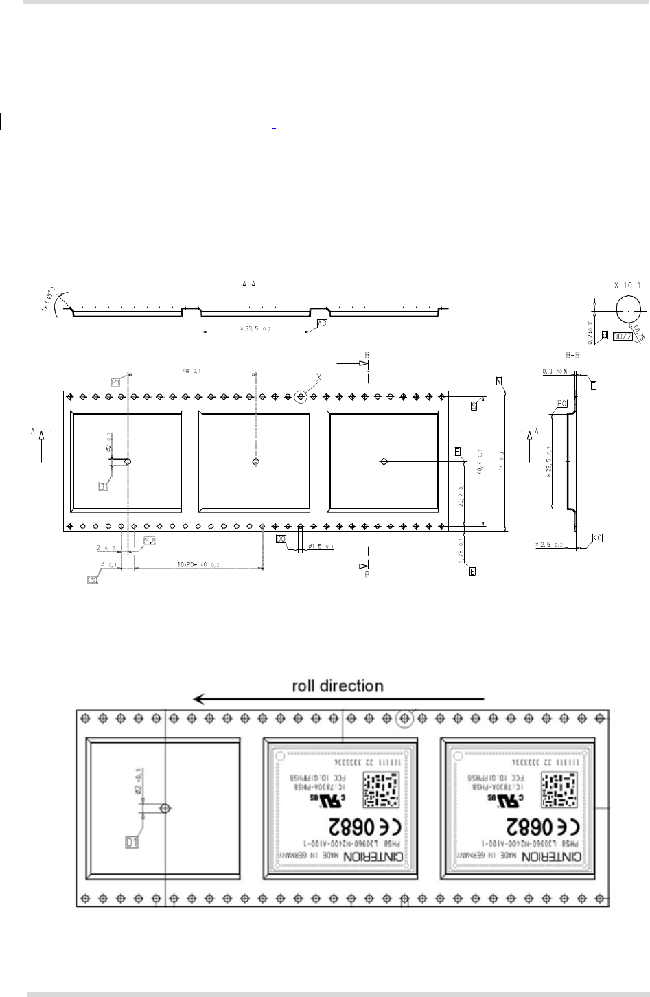
PCS3_HD_v01.000
Confidential / Preliminary Page 89 of 101 2013-10-21
PCS3 Hardware Interface Description
7.3 Packaging
7.3
Packaging
7.3.1
Tape and Reel
The single-feed tape carrier for PCS3 is illustrated in Figure 41. The figure also shows the prop-
er part orientation. The tape width is 44mm and the PCS3 modules are placed on the tape with
a 40mm pitch. The reels are 330mm in diameter with 100mm hubs. Each reel contains 500
modules.
7.3.1.1
Orientation
Figure 41: Carrier tape
Figure 42: Roll direction

PCS3_HD_v01.000
Confidential / Preliminary Page 90 of 101 2013-10-21
PCS3 Hardware Interface Description
7.3 Packaging
7.3.1.2
Barcode Label
A barcode label provides detailed information on the tape and its contents. It is attached to the
reel.
Barcode label
Figure 43: Barcode label on tape reel

PCS3_HD_v01.000
Confidential / Preliminary Page 91 of 101 2013-10-21
PCS3 Hardware Interface Description
7.3 Packaging
7.3.2
Shipping Materials
PCS3 is distributed in tape and reel carriers. The tape and reel carriers used to distribute PCS3
are packed as described below, including the following required shipping materials:
•
Moisture barrier bag, including desiccant and humidity indicator card
•
Transportation bag
7.3.2.1
Moisture Barrier Bag
The tape reels are stored inside an MBB (=moisture barrier bag), together with a humidity indi-
cator card and desiccant pouches - see Figure 44. The bag is ESD protected and delimits mois-
ture transmission. It is vacuum-sealed and should be handled carefully to avoid puncturing or
tearing. The bag protects the PCS3 modules from moisture exposure. It should not be opened
until the devices are ready to be soldered onto the application.
Figure 44: Moisture barrier bag (MBB) with imprint
The label shown in Figure 45 summarizes requirements regarding moisture sensitivity, includ-
ing shelf life and baking requirements. It is attached to the outside of the moisture barrier bag.
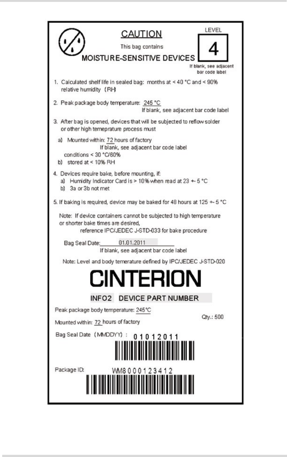
PCS3_HD_v01.000
Confidential / Preliminary Page 92 of 101 2013-10-21
PCS3 Hardware Interface Description
7.3 Packaging
Figure 45: Moisture Sensitivity Label
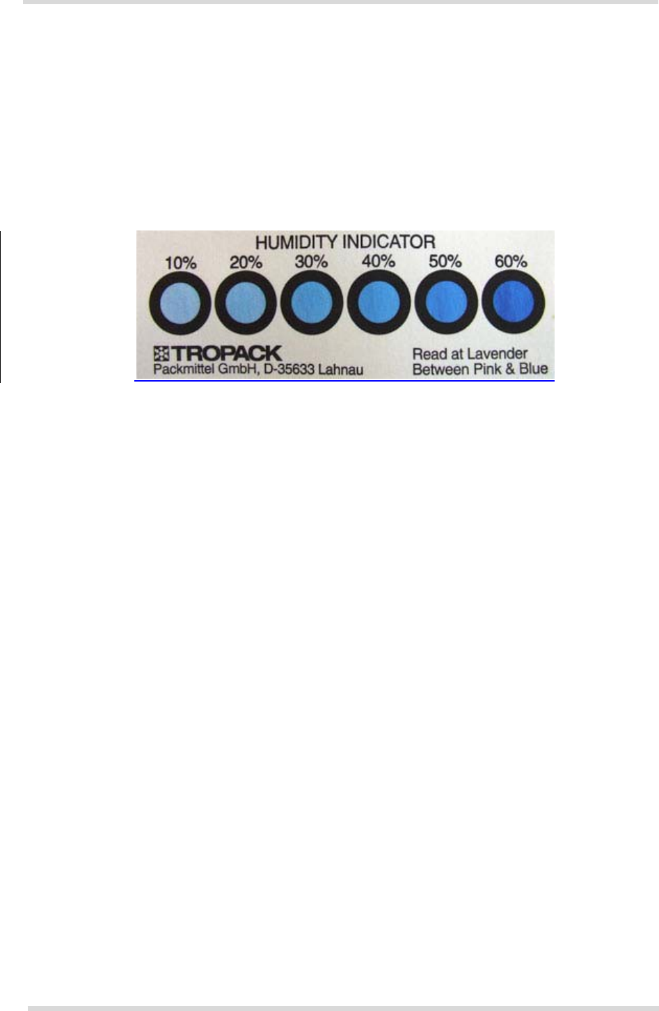
PCS3_HD_v01.000
Confidential / Preliminary Page 93 of 101 2013-10-21
PCS3 Hardware Interface Description
7.3 Packaging
MBBs contain one or more desiccant pouches to absorb moisture that may be in the bag. The
humidity indicator card described below should be used to determine whether the enclosed
components have absorbed an excessive amount of moisture.
The desiccant pouches should not be baked or reused once removed from the MBB.
The humidity indicator card is a moisture indicator and is included in the MBB to show the ap-
proximate relative humidity level within the bag. Sample humidity cards are shown in Figure 46.
If the components have been exposed to moisture above the recommended limits, the units will
have to be rebaked.
Figure 46: Humidity Indicator Card - HIC
A baking is required if the humidity indicator inside the bag indicates 10% RH or more.
7.3.2.2
Transportation Box
Tape and reel carriers are distributed in a box, marked with a barcode label for identification
purposes. A box contains 2 reels with 500 modules each.

PCS3_HD_v01.000
Confidential / Preliminary Page 94 of 101 2013-10-21
PCS3 Hardware Interface Description
8 Sample Application
8
Sample Application
Figure 47 shows a typical example of how to integrate an PCS3 module with an application.
The audio interface demonstrates the balanced connection of microphone and earpiece. This
solution is particularly well suited for internal transducers.
The PWR_IND line is an open collector that needs an external pull-up resistor which connects
to the voltage supply VCC µC of the microcontroller. Low state of the open collector pulls the
PWR_IND signal low and indicates that the PCS3 module is active, high level notifies the Pow-
er-down mode.
If the module is in Power-down mode avoid current flowing from any other source into the mod-
ule circuit, for example reverse current from high state external control lines. Therefore, the
controlling application must be designed to prevent reverse flow. If an external level controller
is required, this can be done by using for example a 5V I/O tolerant buffer/driver like a
"74AVC4T245" with OE (Output Enable) controlled by PWR_IND.
While developing SMT applications it is strongly recommended to provide test points
for certain signals resp. lines to and from the module - for debug and/or test purposes.
The SMT application should allow for an easy access to these signals. For details on
how to implement test points see [4].
The EMC measures are best practice recommendations. In fact, an adequate EMC strategy for
an individual application is very much determined by the overall layout and, especially, the po-
sition of components.
Disclaimer:
No warranty, either stated or implied, is provided on the sample schematic diagram shown in
Figure 47 and the information detailed in this section. As functionality and compliance with na-
tional regulations depend to a great amount on the used electronic components and the indi-
vidual application layout manufacturers are required to ensure adequate design and operating
safeguards for their products using PCS3 modules.
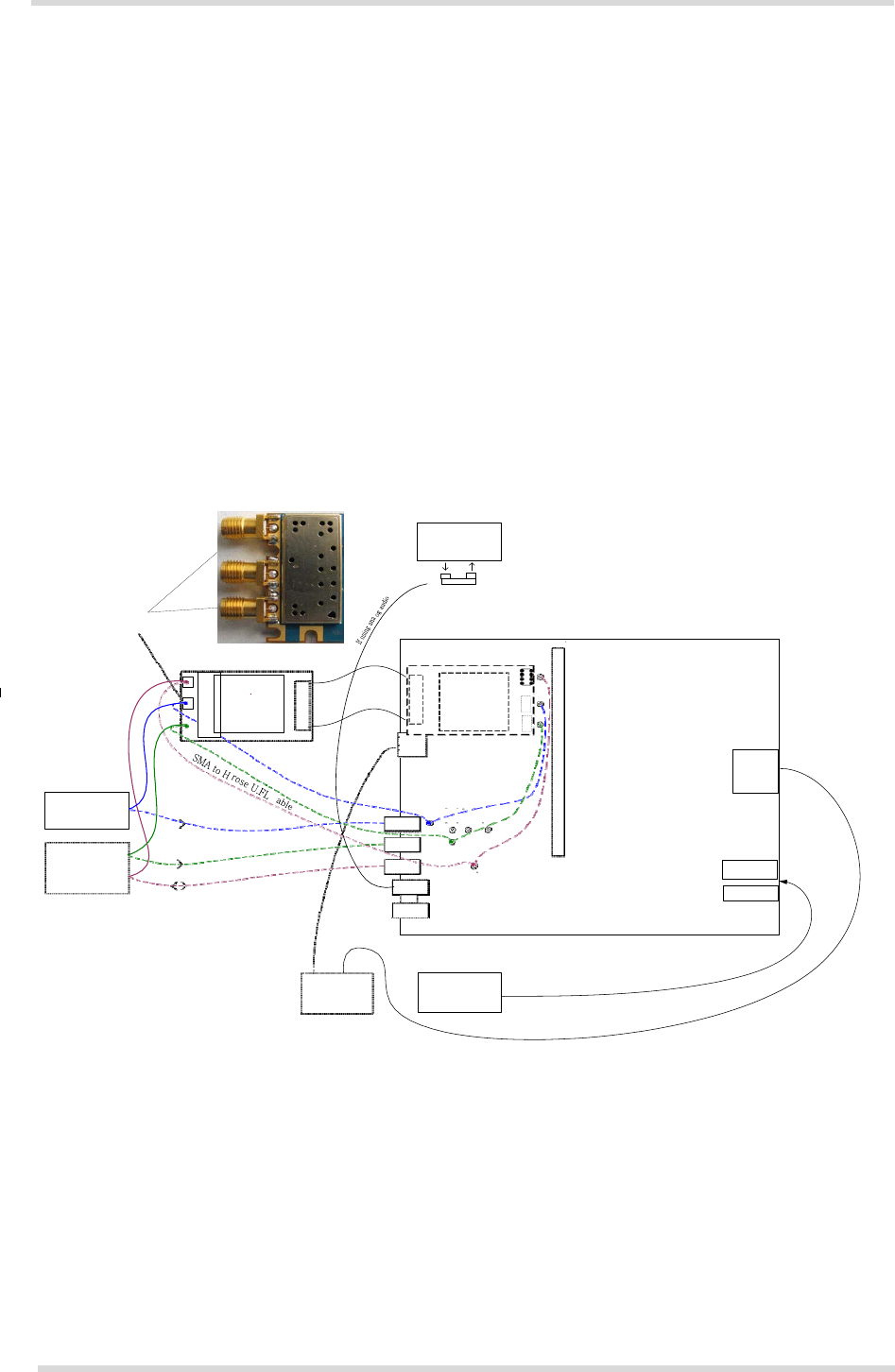
PCS3_HD_v01.000
Confidential / Preliminary Page 95 of 101 2013-10-21
PCS3 Hardware Interface Description
9 Reference Approval
U ra n us
9
Reference Approval
9.1 Reference Equipment for Type Approval
The Cinterion Wireless Modules reference setup submitted to type approve PCS3 is shown in
Figure 48. The module (i.e., the evaluation module) is connected to the DSB75 by means of a
flex cable and a special DSB75 adapter. The CDMA test equipment is connected via
edge
mount SMA connectors soldered to the module’s antenna pads.( (Only Main Antenna of
PCS3, Didn’t have GPS)
For ESD tests and evaluation purposes, it is also possible connect the module to the CDMA
test equipment through an SMA-to-Hirose-U.FL antenna cable and the SMA antenna
connectors of the DSB75 adapter.
A further option is to mount the evaluation module directly onto the DSB75 adapter’s 80-pin
board-to-board connector and to connect the test equipment as shown below.
Aud io
te st equ ipm ent
De tail: Vo tro nic
han dse t
E dg e m o u nt S M A c on n ec to r s
m an ua lly so ld ered to an ten na pa ds
P CS3
eva lua tion
m o dule
S ta n da rd
80 polig Flex
PCS3
evaluation
m odu le
US B
D S B 7 5 a d a p t e r
CO M 1
(ASC 0)
GNS S
test eq uipm en t
GN S S
AN T 3
CD M A
test eq uipm en t
CDM A D rx
C D M A M a in
US B
ca ble
AN T 2
AN T 1
Au dio
A udio
DSB7 5
Pow e r
GN D
Po w er
PC supp ly
RS 2 32
cab le
Figure 48: Reference equipment for type approval

PCS3_HD_v01.000
Confidential / Preliminary Page 96 of 101 2013-10-21
PCS3 Hardware Interface Description
10 Appendix
9.2 Compliance with FCC and IC Rules and Regulations
The Equipment Authorization Certification for the Cinterion Wireless Modules reference appli-
cation described in Section 9.1 will be registered under the following identifiers:
FCC Identifier QIPPCS3
Industry Canada Certification Number: 7830A-PCS3
Granted to Cinterion Wireless Modules GmbH
Manufacturers of mobile or fixed devices incorporating PCS3 modules are authorized to use
the FCC Grants and Industry Canada Certificates of the PCS3 modules for their own final prod-
ucts according to the conditions referenced in these documents. In this case, the FCC label of
the module shall be visible from the outside, or the host device shall bear a second label stating
"Contains FCC ID QIPPCS3" and accordingly “Contains IC 7830A-PCS3“. The integration is
limited to fixed or mobile categorised host devices, where a separation distance between the
antenna and any person of min. 20cm can be assured during normal operating conditions. For
mobile and fixed operation configurations the antenna gain, including cable loss, must not ex-
ceed the limits 9.0 dBi (BC0), 9.0 dBi (BC10) and 7.5 dBi (BC1).
IMPORTANT:
Manufacturers of portable applications incorporating PCS3 modules are required to have their
final product certified and apply for their own FCC Grant and Industry Canada Certificate relat-
ed to the specific portable mobile. This is mandatory to meet the SAR requirements for portable
mobiles (see Section 1.3.1 for detail).
Changes or modifications not expressly approved by the party responsible for compliance
could void the user's authority to operate the equipment.
Note-1: This equipment has been tested and found to comply with the limits for a Class B digital
device, pursuant to part 15 of the FCC Rules and with Industry Canada licence-exempt RSS
standard(s). These limits are designed to provide reasonable protection against harmful inter-
ference in a residential installation. This equipment generates, uses and can radiate radio fre-
quency energy and, if not installed and used in accordance with the instructions, may cause
harmful interference to radio communications. However, there is no guarantee that interference
will not occur in a particular installation. If this equipment does cause harmful interference to
radio or television reception, which can be determined by turning the equipment off and on, the
user is encouraged to try to correct the interference by one or more of the following measures:
•
Reorient or relocate the receiving antenna.
•
Increase the separation between the equipment and receiver.
•
Connect the equipment into an outlet on a circuit different from that to which the receiver
is connected.
•
Consult the dealer or an experienced radio/TV technician for help.
This Class B digital apparatus complies with Canadian ICES-003.
Note-2: This device complies with Part 15 of the FCC Rules. Operation is subject to the
following two conditions: (1) This device may not cause harmful interference, and (2) this
device must accept any interference received, including interference that may cause
undesired operation.
This device complies with Industry Canada license-exempt RSS standard(s). Operation is
subject to the following two conditions:
(1) This device may not cause interference, and
(2) This device must accept any interference, including interference that may cause
undesired operation of the device.

PCS3_HD_v01.000
Confidential / Preliminary Page 97 of 101 2013-10-21
PCS3 Hardware Interface Description
10 Appendix
Le présent appareil est conforme aux CNR d'Industrie Canada applicables aux appareils radio
exempts de licence. L'exploitation est autorisée aux deux conditions suivantes:
(1) l'appareil ne doit pas produire de brouillage, et
(2) l'utilisateur de l'appareil doit accepter tout brouillage radioélectrique subi, même si le
brouillage est susceptible d'en compromettre le fonctionnement."
CAN ICES-3(B)/ NMB-3(B)
10
Appendix
10.1
List of Parts and Accessories
Table 32: List of parts and accessories
Description Supplier Ordering information
PCS3 Cinterion Standard module
Cinterion Wireless Modules IMEI:
Ordering number: L30960-N2650-A280
PCS3 Evaluation Module Cinterion Ordering number: L30960-N2651-TBD.
DSB75 Support Box Cinterion Ordering number: L36880-N8811-A100
DSB75 adapter for mounting
the PCS3 evaluation module Cinterion Ordering number: L30960-N2301-A100
Votronic Handset VOTRONIC Votronic HH-SI-30.3/V1.1/0
VOTRONIC
Entwicklungs- und Produktionsgesellschaft für elek-
tronische Geräte mbH
Saarbrücker Str. 8
66386 St. Ingbert
Germany
Phone: +49-(0)6 89 4 / 92 55-0
Fax: +49-(0)6 89 4 / 92 55-88
Email: contact@votronic.com
U.FL antenna connector Hirose or Molex Sales contacts are listed in Table 34 and Table 35.

PCS3_HD_v01.000
Confidential / Preliminary Page 98 of 101 2013-10-21
PCS3 Hardware Interface Description
10.1 List of Parts and Accessories
Table 33: Molex sales contacts (subject to change)
Molex
For further information please click:
http://www.molex.com
Molex Deutschland GmbH
Otto-Hahn-Str. 1b
69190 Walldorf
Germany
Phone: +49-6227-3091-0
Fax: +49-6227-3091-8100
Email: mxgermany@molex.com
American Headquarters
Lisle, Illinois 60532
U.S.A.
Phone: +1-800-78MOLEX
Fax: +1-630-969-1352
Molex China Distributors
Beijing,
Room 1311, Tower B, COFCO Plaza
No. 8, Jian Guo Men Nei Street, 100005
Beijing
P.R. China
Phone: +86-10-6526-9628
Fax: +86-10-6526-9730
Molex Singapore Pte. Ltd.
110, International Road
Jurong Town,
Singapore 629174
Phone: +65-6-268-6868
Fax: +65-6-265-6044
Molex Japan Co. Ltd.
1-5-4 Fukami-Higashi,
Yamato-City,
Kanagawa, 242-8585
Japan
Phone: +81-46-265-2325
Fax: +81-46-265-2365
Table 34: Hirose sales contacts (subject to change)
Hirose Ltd.
For further information please click:
http://www.hirose.com
Hirose Electric (U.S.A.) Inc
2688 Westhills Court
Simi Valley, CA 93065
U.S.A.
Phone: +1-805-522-7958
Fax: +1-805-522-3217
Hirose Electric Europe B.V.
German Branch:
Herzog-Carl-Strasse 4
73760 Ostfildern
Germany
Phone: +49-711-456002-1
Fax: +49-711-456002-299
Email:info@hirose.de
Hirose Electric Europe B.V.
UK Branch:
First Floor, St. Andrews House,
Caldecotte Lake Business Park,
Milton Keynes MK7 8LE
Great Britain
Phone: +44-1908-369060
Fax: +44-1908-369078
Hirose Electric Co., Ltd.
5-23, Osaki 5 Chome,
Shinagawa-Ku
Tokyo 141
Japan
Phone: +81-03-3491-9741
Fax: +81-03-3493-2933
Hirose Electric Europe B.V.
Hogehillweg 8
1101 CC Amsterdam Z-O
Netherlands
Phone: +31-20-6557-460
Fax: +31-20-6557-469

PCS3_HD_v01.000
Confidential / Preliminary Page 99 of 101 2013-10-21
PCS3 Hardware Interface Description
10.2 Mounting Advice Sheet
10.2
Mounting Advice Sheet
To prevent mechanical damage, be careful not to force, bend or twist the module. Be sure it is
soldered flat against the host device (see also Section 7.2). The advice sheet on the next page
shows a number of examples for the kind of bending that may lead to mechanical damage of
the module (the module as part of an external application is integrated into a housing).
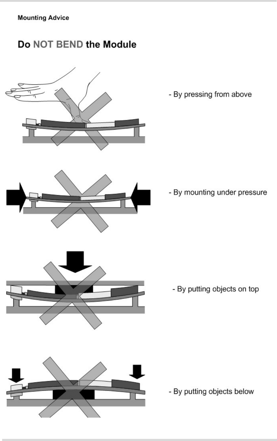
PCS3_HD_v01.000
Confidential / Preliminary Page 100 of 101 2013-10-21
PCS3 Hardware Interface Description
10.2 Mounting Advice Sheet