Contents
user manual part 1

Customer Services
Mobile Radio Division
Tait Electronics Ltd
PO Box 1645
Christchurch
New Zealand
Fax: (64) (3) 358-3903
Company Name ___________________________
Name ___________________________
Department ___________________________
Street or PO Box ___________________________
Town and Postcode ___________________________
Country ___________________________
Manual Product Code M___________-______-_______
So that you are kept up to date with documentation relevant to this product, please fill out
and return this registration form.
Do you wish to be notified by your Tait subsidiary when Revision Packages are available, so
that you can keep this manual up to date? Yes
Would you like to know about technical training services? Yes
In order to improve our documentation, we would like your opinion of this manual. Please
put a mark in the column that best describes your opinion.
Comments: _______________________________________________________________________
_________________________________________________________________________________
Is there any additional documentation we should provide?______________________________
_________________________________________________________________________________
What industry are you in (e.g. Telecomms, Security, Forestry)?___________________________
Do you use other Tait products?
poor average excellent
Technical Depth
Technical Accuracy
Readability
Ease of Use
Document Format
Overall Satisfaction
T2000 T700 T800 Mobile Data Trunking Other


Tait Electronics Ltd
558 Wairakei Road
P.O. Box 1645
Christchurch
New Zealand
Phone: 64 3 358-3399
Fax: 64 3 358-3636
Tait Electronics (Aust) Pty Ltd
275 Toombul Road
Northgate 4013
P.O. Box 679
Virginia
Queensland 4014
Australia
Phone: 61 7 3865-7799
Toll Free: 1 300 304-344
Fax: 61 7 3865-7990
E-mail: helpdesk@tait.com.au
Tait Mobile Radio Inc.
Unit 5, 158 Anderson Avenue
Markham
Ontario L6E1A9
Canada
Phone: 1 905 472-1100
Fax: 1 905 472-5300
E-mail: 110252.44@compuserve.com
Tait France S.A.R.L.
2 avenue de la Cristallerie
92 316 Sèvres, Cedex
France
Phone: 33 1 41 14-05-50
Fax: 33 1 41 14-05-55
E-mail: 100675.651@compuserve.com
Tait Mobilfunk GmbH
Willstätterstraße 50
D-90449 Nürnberg 60
Germany
Phone: 49 911 967-460
Fax: 49 911 967-4679
E-mail: tait@t-online.de
Tait Mobile Radio (Hong Kong) Ltd
Room 703A New East Ocean
Centre
9 Science Museum Road
Tsim Sha Tsui East
Hong Kong
Phone: 852 2369-3040
Fax: 852 2369-3009
E-mail: 106122.2060@compuserve.com
Tait Communications Ltd
Unit 4, 75 Blenheim Road
P.O. Box 1185
Christchurch
Phone: 64 3 348-3301
Fax: 64 3 343-0558
E-mail: nsc@tcl.tait.co.nz
Tait Electronics (Far East) Pte Ltd
4 Leng Kee Road
SIS Building #05-11A
Singapore 159088
Phone: 65 471-2688
Fax: 65 479-7778
E-mail: taittfe@singnet.com.sg
Tait Mobile Radio (Taiwan) Ltd
1104, 142 Chung Hsiao E Rd
Sec 4
Taipei
Taiwan
Phone: 886 2 2731-1290
Fax: 886 2 2711-6351
E-mail: tait8503@ms7.hinet.net
Tait Mobile Radio Ltd
14/1 Suwan Tower, Ground Floor
Soi Saladaeng 1
North Sathorn Rd
Bangrak
Bangkok 10500
Thailand
Phone: 662 267-6290
Fax: 662 267-6293
E-mail: taitthd@loxinfo.co.th
Tait Mobile Radio Ltd
Ermine Business Park
Ermine Road
Huntingdon
Cambridgeshire PE18 6YA
United Kingdom
Phone: 44 1480-52255
Fax: 44 1480-411996
E-mail: techsupport@tait.co.uk
Tait Electronics (USA) Inc.
9434 Old Katy Road
Suite 110
Houston
Texas 77055
USA
Phone: 1 713 984-8684
Toll Free: 1 800 222-1255
Fax: 1 713 468-6944
E-mail: tech@taitus.com
!
This manual contains general, technical and servicing informa-
tion on T2000 Series II mobile two-way radios.
We have published this manual in a ring binder so that “revision
packages” containing additional information can be added as
required.
Revision packages will normally be published to coincide with
the release of information on a new PCB, and may also contain
additions or corrections pertaining to other parts of the manual.
If you return the customer registration card at the front of this
manual, you will be notified when revision packages containing
new PCB information and/or text are available. You may then
order as many packages as you require from your local Tait
Company. Revision packages are supplied ready-punched for
inclusion in your manual.
Each page in this manual has a date of issue. This is to comply
with various Quality Standards, but will also serve to identify
which pages have been updated and when. Each page and its
publication date is listed in the “List of Effective Pages”, and a
new list containing any new/revised pages and their publica-
tion dates will be sent with each revision package.
Any portion of text that has been changed is marked by a verti-
cal line (as shown at left) in the outer margin of the page. Where
the removal of an entire paragraph means there is no text left to
mark, an arrow (as shown at left) will appear in the outer mar-
gin. The number beside the arrow will indicate how many para-
graphs have been deleted.
The manual issue and revision status are indicated by the last
three digits of the manual product code. These digits start at 100
and will increment through 101, 102, 103, etc., as revision pack-
ages are published, e.g:
Thus, Issue 301 indicates the first revision to issue 3, and means
that one package should have been added to the manual. The
issue digit will only change if there is a major product revision,
or if the number of revision packages to be included means that
the manual becomes difficult to use, at which point a new issue
manual will be published in a new ring binder.
PCB information is provided for all current issue PCBs, as well
as all previous issue PCBs manufactured in production quanti-
ties, and is grouped according to PCB. Thus, you will find the
parts list, grid reference index (if necessary), PCB layouts and
circuit diagram(s) for each individual PCB grouped together.
2
3 0 1
issue status revision status

"
If you find an error in this manual, or have a suggestion on how
it might be improved, please do not hesitate to contact the Tech-
nical Writer, Product Support Group, Tait Mobile Radio Divi-
sion, Tait Electronics Ltd, P.O. Box 1645, Christchurch, New
Zealand.
##$
Any enquiries regarding this manual or the equipment it describes should be addressed
in the first instance to your nearest approved Tait Dealer or Service Centre. Further tech-
nical assistance may be obtained from the Product Support Group, Tait Mobile Radio
Division, Tait Electronics Ltd, Christchurch, New Zealand.
%&'(&!
In the interests of improving performance, reliability or servicing, Tait Electronics Ltd
reserve the right to update their equipment and/or manuals without prior notice.
)&
All information contained in this manual is the property of Tait Electronics Ltd. All
rights are reserved. This manual may not, in whole or part, be copied, photocopied,
reproduced, translated stored or reduced to any electronic medium or machine readable
form without prior written permission from Tait Electronics Ltd.
*#
Service Manuals should be ordered from your nearest Tait Branch or approved Dealer.
When ordering, quote the Tait product code and, where applicable, the version.
*$
M2000-00-300 T2000 Series II Service Manual
Issue 300 published January 1997
Issue 301 published March 1998

+
,*'#
The total number of pages in this Manual is 484, as listed below.
Page Issue Date
131/12/97
231/12/97
331/10/96
431/10/96
531/12/97
631/12/97
731/12/97
831/12/97
931/12/97
10 31/10/96
11 31/12/97
12 31/12/97
13 31/12/97
14 31/12/97
15 31/12/97
16 31/12/97
17 31/12/97
18 31/12/97
19 31/12/97
20 31/12/97
1.1 31/10/96
1.2 31/10/96
1.3 31/10/96
1.4 31/10/96
1.5 31/12/97
1.6 31/12/97
1.7 31/10/96
1.8 31/10/96
1.9 31/12/97
1.10 31/10/96
2.1 31/10/96
2.2 31/10/96
2.3 31/10/96
2.4 31/10/96
2.5 31/10/96
2.6 31/10/96
2.7 31/10/96
2.8 31/10/96
2.9 31/10/96
2.10 31/10/96
2.11 31/10/96
2.12 31/10/96
2.13 31/10/96
2.14 31/10/96
2.15 31/10/96
2.16 31/10/96
2.17 31/10/96
2.18 31/10/96
2.19 31/10/96
2.20 blank
3.1 31/12/97
3.2 31/10/96
3.3 31/10/96
3.4 31/10/96
3.5 31/10/96
3.6 31/12/97
3.7 31/10/96
3.8 31/10/96
3.9 31/12/97
3.10 31/12/97
3.11 31/12/97
3.12 31/10/96
3.13 31/10/96
3.14 31/10/96
3.15 31/10/96
3.16 31/10/96
3.17 31/10/96
3.18 31/10/96
4.1 31/10/96
4.2 31/12/97
4.3 31/10/96
4.4 31/10/96
4.5 31/10/96
4.6 31/10/96
4.7 31/10/96
4.8 31/10/96
4.9 31/10/96
4.10 31/10/96
4.11 31/10/96
4.12 blank
5.1 31/10/96
5.2 31/10/96
5.3 31/10/96
5.4 31/10/96
5.5 31/10/96
5.6 31/10/96
5.7 31/10/96
5.8 31/10/96
5.9 31/10/96
5.10 31/10/96
5.11 31/10/96
5.12 31/10/96
5.13 31/10/96
5.14 31/10/96
5.15 31/10/96
5.16 31/10/96

-
5.17 31/10/96
5.18 31/10/96
5.19 31/10/96
5.20 31/10/96
5.21 31/10/96
5.22 31/10/96
5.23 31/10/96
5.24 31/10/96
5.25 31/10/96
5.26 31/10/96
5.27 31/10/96
5.28 31/10/96
5.29 31/10/96
5.30 31/10/96
5.31 31/10/96
5.32 31/10/96
6.1 31/12/97
6.2 31/10/96
6.3 31/12/97
6.4 31/12/97
6.5 31/10/96
6.6 31/10/96
6.7 31/12/97
6.8 31/12/97
6.9 31/10/96
6.10 31/10/96
7.1 31/12/97
7.2 31/10/96
7.3 31/10/96
7.4 31/10/96
7.1.1 31/10/96
7.1.2 31/10/96
7.1.3 31/10/96
7.1.4 blank
7.1.5 31/10/96
7.1.6 31/10/96
7.1.7 31/10/96
7.1.8 31/10/96
7.1.9 31/10/96 (fold-out)
7.1.10 blank
7.2.1 31/10/96
7.2.2 31/10/96
7.2.3 31/10/96
7.2.4 31/10/96
7.2.5 31/10/96
7.2.6 31/10/96
7.2.7 31/10/96
7.2.8 31/10/96
7.2.9 31/10/96 (fold-out)
7.2.10 31/10/96 (fold-out)
7.3.1 31/10/96
7.3.2 31/10/96
7.3.3 31/10/96
7.3.4 31/10/96
7.3.5 31/10/96
7.3.6 31/10/96
7.3.7 31/10/96
7.3.8 31/10/96
7.3.9 31/10/96 (fold-out)
7.3.10 31/10/96 (fold-out)
7.4.1 31/10/96
7.4.2 31/10/96
7.4.3 31/10/96
7.4.4 31/10/96
7.4.5 31/10/96
7.4.6 31/10/96
7.4.7 31/10/96
7.4.8 31/10/96
7.4.9 31/10/96 (fold-out)
7.4.10 31/10/96 (fold-out)
7.5.1 31/10/96
7.5.2 31/10/96
7.5.3 31/10/96
7.5.4 31/10/96
7.5.5 31/10/96
7.5.6 31/10/96
7.5.7 31/10/96
7.5.8 31/10/96
7.5.9 31/10/96 (fold-out)
7.5.10 31/10/96 (fold-out)
7.6.1 31/10/96
7.6.2 31/10/96
7.6.3 31/10/96
7.6.4 31/10/96
7.6.5 31/10/96
7.6.6 31/10/96
7.6.7 31/10/96
7.6.8 31/10/96
7.6.9 31/10/96 (fold-out)
7.6.10 blank
7.6.11 31/12/97
7.6.12 31/12/97
7.6.13 31/12/97
7.6.14 31/12/97
7.6.15 31/12/97
7.6.16 31/12/97
7.6.17 31/12/97
7.6.18 31/12/97
7.6.19 31/12/97 (fold-out)
7.6.20 blank
7.7.1 31/12/97
7.7.2 31/10/96
7.7.3 31/10/96
7.7.4 31/10/96
7.7.5 31/10/96
7.7.6 31/10/96
7.7.7 31/10/96
7.7.8 31/10/96

.
7.7.9 31/10/96 (fold-out)
7.7.10 blank
7.8.1 31/10/96
7.8.2 blank
7.8.3 31/10/96
7.8.4 31/10/96
7.8.5 31/10/96 (fold-out)
7.8.6 blank
7.9.1 31/12/97
7.9.2 blank
7.9.3 31/10/96
7.9.4 31/10/96
7.9.5 31/10/96 (fold-out)
7.9.6 blank
7.9.7 31/12/97
7.9.8 31/12/97
7.9.9 31/12/97
7.9.10 31/12/97
7.9.11 31/12/97 (fold-out)
7.9.12 blank
7.10.1 31/10/96
7.10.2 31/10/96
7.10.3 31/10/96
7.10.4 31/10/96
7.10.5 31/10/96
7.10.6 31/10/96
7.10.7 31/10/96 (fold-out)
7.10.8 31/10/96 (fold-out)
7.10.9 31/10/96 (fold-out)
7.10.10 blank
7.10.11 31/12/97
7.10.12 31/12/97
7.10.13 31/12/97
7.10.14 31/12/97
7.10.15 31/12/97
7.10.16 31/12/97
7.10.17 31/12/97 (fold-out)
7.10.18 31/12/97 (fold-out)
7.10.19 31/12/97 (fold-out)
7.10.20 blank
7.10.21 31/12/97
7.10.22 31/12/97
7.10.23 31/12/97
7.10.24 31/12/97
7.10.25 31/12/97
7.10.26 31/12/97
7.10.27 31/12/97 (fold-out)
7.10.28 31/12/97 (fold-out)
7.10.29 31/12/97 (fold-out)
7.10.30 blank
7.11.1 31/10/96
7.11.2 31/10/96
7.11.3 31/10/96
7.11.4 31/10/96
7.11.5 31/10/96
7.11.6 31/10/96
7.11.7 31/10/96 (fold-out)
7.11.8 31/10/96 (fold-out)
7.11.9 31/10/96 (fold-out)
7.11.10 blank
7.11.11 31/10/96 (fold-out)
7.11.12 blank
7.11.13 31/12/97
7.11.14 31/12/97
7.11.15 31/12/97
7.11.16 31/12/97
7.11.17 31/12/97
7.11.18 31/12/97
7.11.19 31/12/97 (fold-out)
7.11.20 31/12/97 (fold-out)
7.11.21 31/12/97 (fold-out)
7.11.22 blank
7.11.23 31/12/97 (fold-out)
7.11.24 blank
7.12.1 31/12/97
7.12.2 31/12/97
7.12.3 31/10/96
7.12.4 31/10/96
7.12.5 31/10/96 (fold-out)
7.12.6 blank
7.13.1 31/12/97
7.13.2 31/12/97
7.13.3 31/10/96
7.13.4 31/10/96
7.13.5 31/10/96 (fold-out)
7.13.6 blank
7.14.1 31/12/97
7.14.2 31/12/97
7.14.3 31/12/97
7.14.4 blank
7.14.5 31/10/96
7.14.6 31/10/96
7.14.7 31/10/96 (fold-out)
7.14.8 blank
7.15.1 31/12/97
7.15.2 31/12/97
7.15.3 31/10/96
7.15.4 31/10/96
7.15.5 31/10/96 (fold-out)
7.15.6 blank
7.16.1 31/12/97
7.16.2 blank
7.16.3 31/10/96
7.16.4 31/10/96
7.16.5 31/10/96
7.16.6 blank
7.17.1 31/12/97
7.17.2 blank

/
7.17.3 31/10/96
7.17.4 31/10/96
7.17.5 31/10/96
7.17.6 blank
8.1 31/12/97
8.2 31/10/96
8.1.1 31/10/96
8.1.2 31/10/96
8.1.3 31/10/96
8.1.4 31/10/96
8.1.5 31/10/96
8.1.6 31/10/96
8.1.7 31/10/96
8.1.8 31/10/96
8.1.9 31/10/96
8.1.10 31/10/96
8.1.11 31/10/96
8.1.12 31/10/96
8.1.13 31/10/96
8.1.14 31/10/96
8.1.15 31/10/96
8.1.16 31/10/96
8.1.17 31/12/97
8.1.18 31/10/96
8.1.19 31/10/96
8.1.20 31/10/96
8.1.21 31/10/96
8.1.22 31/10/96
8.1.23 31/10/96
8.1.24 blank
8.2.1 31/10/96
8.2.2 31/10/96
8.3.1 31/10/96
8.3.2 31/10/96
8.3.3 31/10/96
8.3.4 31/10/96
8.4.1 31/10/96
8.4.2 31/10/96
8.5.1 31/10/96
8.5.2 31/10/96
8.5.3 31/10/96
8.5.4 blank
8.6.1 31/10/96
8.6.2 31/10/96
8.6.3 31/10/96
8.6.4 31/10/96
8.7.1 31/10/96
8.7.2 31/10/96
8.7.3 31/10/96
8.7.4 31/10/96
8.8.1 31/10/96
8.8.2 31/10/96
8.8.3 31/10/96
8.8.4 31/10/96
8.8.5 31/10/96
8.8.6 31/10/96
8.8.7 31/10/96
8.8.8 blank
8.9.1 31/10/96
8.9.2 blank
8.10.1 31/12/97
8.10.2 31/12/97
8.10.3 31/12/97
8.10.4 31/12/97
8.10.5 31/12/97
8.10.6 blank
8.10.7 31/12/97
8.10.8 31/12/97
8.10.9 31/12/97
8.10.10 31/12/97
8.11.1 31/10/96
8.11.2 31/10/96
8.11.3 31/10/96
8.11.4 31/10/96
8.11.5 31/10/96
8.11.6 31/10/96
8.11.7 31/10/96
8.11.8 31/10/96
8.11.9 31/10/96
8.11.10 31/10/96
8.11.11 31/10/96
8.11.12 31/10/96
8.11.13 31/10/96
8.11.14 31/10/96
8.11.15 31/10/96 fold-out
8.11.16 blank
8.11.17 31/10/96 fold-out
8.11.18 blank
8.12.1 31/10/96
8.12.2 31/10/96
8.12.3 31/10/96
8.12.4 31/10/96
8.12.5 31/12/97
8.12.6 31/10/96
8.12.7 31/10/96
8.12.8 31/10/96
8.12.9 31/10/96
8.12.10 31/10/96
8.12.11 31/10/96
8.12.12 31/10/96
8.12.13 31/10/96
8.12.14 blank
8.13.1 31/12/97
8.13.2 31/12/97
8.13.3 31/12/97
8.13.4 31/12/97
8.13.5 31/12/97
8.13.6 31/12/97

0
8.13.7 31/12/97
8.13.8 blank
8.14.1 31/10/96
8.14.2 31/10/96
8.14.3 31/10/96
8.14.4 31/10/96
8.14.5 31/10/96
8.14.6 31/10/96
8.14.7 31/10/96
8.14.8 31/10/96
8.14.9 31/10/96
8.14.10 31/10/96
8.14.11 31/10/96
8.14.12 31/10/96
8.14.13 31/10/96
8.14.14 31/10/96
8.14.15 31/10/96
8.14.16 31/10/96
8.14.17 31/10/96
8.14.18 31/10/96
8.14.19 31/10/96
8.14.20 31/10/96
8.14.21 31/10/96
8.14.22 31/10/96
8.14.23 31/10/96
8.14.24 31/10/96
8.14.25 31/10/96
8.14.26 31/10/96
8.14.27 31/10/96 fold-out
8.14.28 blank
8.15.1 31/12/97
8.15.2 31/12/97
8.15.3 31/12/97
8.15.4 31/12/97
8.15.5 31/12/97
8.15.6 31/12/97
8.15.7 31/12/97
8.15.8 31/12/97
8.15.9 31/12/97
8.15.10 31/12/97
8.15.11 31/12/97
8.15.12 31/12/97
8.15.13 31/12/97
8.15.14 31/12/97
8.15.15 31/12/97
8.15.16 31/12/97
8.15.17 31/12/97
8.15.18 blank
8.16.1 31/12/97
8.16.2 31/12/97
8.16.3 31/12/97
8.16.4 31/12/97
8.16.5 31/12/97
8.16.6 31/12/97
8.16.7 31/12/97
8.16.8 blank
9.1 31/10/96
9.2 31/10/96
9.3 31/10/96
9.4 31/10/96
9.5 31/10/96
9.6 31/10/96
9.7 31/10/96
9.8 31/10/96

1
)
2$
1.1 Introduction . . . . . . . . . . . . . . . . . . . . . . . . . . . . . . . . . . . . . . . . . . . . . . . . . . . . . . . . . .1.2
1.2 Specifications . . . . . . . . . . . . . . . . . . . . . . . . . . . . . . . . . . . . . . . . . . . . . . . . . . . . . . . . .1.3
1.2.1 Introduction. . . . . . . . . . . . . . . . . . . . . . . . . . . . . . . . . . . . . . . . . . . . . . . . . . .1.3
1.2.2 General. . . . . . . . . . . . . . . . . . . . . . . . . . . . . . . . . . . . . . . . . . . . . . . . . . . . . . .1.3
1.2.3 Receiver Performance . . . . . . . . . . . . . . . . . . . . . . . . . . . . . . . . . . . . . . . . . .1.5
1.2.4 Transmitter Performance . . . . . . . . . . . . . . . . . . . . . . . . . . . . . . . . . . . . . . .1.7
1.2.5 Frequency Reference . . . . . . . . . . . . . . . . . . . . . . . . . . . . . . . . . . . . . . . . . . .1.8
1.2.6 Trunking . . . . . . . . . . . . . . . . . . . . . . . . . . . . . . . . . . . . . . . . . . . . . . . . . . . . .1.9
1.2.6.1 T2030, T2035, T2040 & T2050 Models . . . . . . . . . . . . . . . . . . . . . . . . . . . . .1.9
1.2.6.2 T2060 Model . . . . . . . . . . . . . . . . . . . . . . . . . . . . . . . . . . . . . . . . . . . . . . . . . .1.9
1.3 Operating Instructions . . . . . . . . . . . . . . . . . . . . . . . . . . . . . . . . . . . . . . . . . . . . . . . . .1.9
1.4 Product Codes . . . . . . . . . . . . . . . . . . . . . . . . . . . . . . . . . . . . . . . . . . . . . . . . . . . . . . .1.10
)##&
2.1 Design Overview . . . . . . . . . . . . . . . . . . . . . . . . . . . . . . . . . . . . . . . . . . . . . . . . . . . . . .2.2
2.2 Synthesiser . . . . . . . . . . . . . . . . . . . . . . . . . . . . . . . . . . . . . . . . . . . . . . . . . . . . . . . . . . .2.3
2.3 Audio & Regulators. . . . . . . . . . . . . . . . . . . . . . . . . . . . . . . . . . . . . . . . . . . . . . . . . . . .2.4
2.4 TCXO/TX Audio PCB. . . . . . . . . . . . . . . . . . . . . . . . . . . . . . . . . . . . . . . . . . . . . . . . . .2.4
2.5 IF PCB . . . . . . . . . . . . . . . . . . . . . . . . . . . . . . . . . . . . . . . . . . . . . . . . . . . . . . . . . . . . . . .2.5
2.6 T2000-100 & -400 RF PCB . . . . . . . . . . . . . . . . . . . . . . . . . . . . . . . . . . . . . . . . . . . . . . .2.6
2.6.1 T2000-100 & -400 Receiver . . . . . . . . . . . . . . . . . . . . . . . . . . . . . . . . . . . . . .2.6
2.6.2 T2000-100 & -400 Exciter . . . . . . . . . . . . . . . . . . . . . . . . . . . . . . . . . . . . . . . .2.7
2.6.3 T2000-100 & -400 Power Amplifier . . . . . . . . . . . . . . . . . . . . . . . . . . . . . . .2.7
2.7 T2000-200 RF PCB . . . . . . . . . . . . . . . . . . . . . . . . . . . . . . . . . . . . . . . . . . . . . . . . . . . . .2.8
2.7.1 T2000-200 Receiver. . . . . . . . . . . . . . . . . . . . . . . . . . . . . . . . . . . . . . . . . . . . .2.8
2.7.2 T2000-200 Exciter . . . . . . . . . . . . . . . . . . . . . . . . . . . . . . . . . . . . . . . . . . . . . .2.9
2.7.3 T2000-200 Power Amplifier . . . . . . . . . . . . . . . . . . . . . . . . . . . . . . . . . . . . .2.9
2.8 T2000-300 RF PCB . . . . . . . . . . . . . . . . . . . . . . . . . . . . . . . . . . . . . . . . . . . . . . . . . . . .2.10
2.8.1 T2000-300 Receiver. . . . . . . . . . . . . . . . . . . . . . . . . . . . . . . . . . . . . . . . . . . .2.10
2.8.2 T2000-300 Exciter . . . . . . . . . . . . . . . . . . . . . . . . . . . . . . . . . . . . . . . . . . . . .2.11
2.8.3 T2000-300 Power Amplifier . . . . . . . . . . . . . . . . . . . . . . . . . . . . . . . . . . . .2.11
2.9 T2000-500, T2000-600, T2000-700, -900 & -000 RF PCB. . . . . . . . . . . . . . . . . . . . . .2.12
2.9.1 T2000-500, -600, -700, -900 & -000 Receiver . . . . . . . . . . . . . . . . . . . . . . .2.12
2.9.2 T2000-500, -600, -700 -900 & -000 Exciter . . . . . . . . . . . . . . . . . . . . . . . . .2.13
2.9.3 T2000-500, -600, -700, -900 & -000 Power Amplifier. . . . . . . . . . . . . . . .2.13

2.10 T2000-800 RF PCB . . . . . . . . . . . . . . . . . . . . . . . . . . . . . . . . . . . . . . . . . . . . . . . . . . . .2.14
2.10.1 T2000-800 Receiver. . . . . . . . . . . . . . . . . . . . . . . . . . . . . . . . . . . . . . . . . . . . 2.14
2.10.2 T2000-800 Exciter . . . . . . . . . . . . . . . . . . . . . . . . . . . . . . . . . . . . . . . . . . . . . 2.15
2.10.3 T2000-800 Power Amplifier. . . . . . . . . . . . . . . . . . . . . . . . . . . . . . . . . . . .2.15
2.11 Control Module . . . . . . . . . . . . . . . . . . . . . . . . . . . . . . . . . . . . . . . . . . . . . . . . . . . . . .2.16
2.11.1 T2010 & T2015 HC05 Logic PCB . . . . . . . . . . . . . . . . . . . . . . . . . . . . . . . .2.16
2.11.2 T2020, T203X, T2040, T2050 & T2060 HC11 Logic PCB . . . . . . . . . . . . .2.19
$##
3.1 Servicing Precautions . . . . . . . . . . . . . . . . . . . . . . . . . . . . . . . . . . . . . . . . . . . . . . . . . .3.2
3.1.1 Caution: Accidental Transmit . . . . . . . . . . . . . . . . . . . . . . . . . . . . . . . . . . . 3.2
3.1.2 Caution: Antenna Loading. . . . . . . . . . . . . . . . . . . . . . . . . . . . . . . . . . . . . .3.2
3.1.3 Caution: Beryllium Oxide & Power Transistors . . . . . . . . . . . . . . . . . . . .3.2
3.1.4 Caution: CMOS Devices . . . . . . . . . . . . . . . . . . . . . . . . . . . . . . . . . . . . . . . .3.2
3.1.5 Caution: Screw Head Types. . . . . . . . . . . . . . . . . . . . . . . . . . . . . . . . . . . . .3.3
3.2 Disassembly Instructions . . . . . . . . . . . . . . . . . . . . . . . . . . . . . . . . . . . . . . . . . . . . . . .3.5
3.2.1 To Gain Access To The Logic PCB. . . . . . . . . . . . . . . . . . . . . . . . . . . . . . . .3.5
3.2.2 To Remove The Bottom Cover And Microprocessor Shield . . . . . . . . . .3.5
3.2.3 To Detach The Control Head . . . . . . . . . . . . . . . . . . . . . . . . . . . . . . . . . . . .3.6
3.2.3.1 Locally Mounted Models . . . . . . . . . . . . . . . . . . . . . . . . . . . . . . . . . . . . . . .3.6
3.2.3.2 Remotely Mounted Models . . . . . . . . . . . . . . . . . . . . . . . . . . . . . . . . . . . . . 3.6
3.2.4 To Disassemble The Control Head . . . . . . . . . . . . . . . . . . . . . . . . . . . . . . .3.7
3.2.4.1 T2010, T2015, T203X & T2060 Radios . . . . . . . . . . . . . . . . . . . . . . . . . . . . .3.7
3.2.4.2 T2020, T2040 & T2050 Radios. . . . . . . . . . . . . . . . . . . . . . . . . . . . . . . . . . . .3.9
3.2.5 To Detach The EMC Filter PCB . . . . . . . . . . . . . . . . . . . . . . . . . . . . . . . . .3.11
3.2.6 To Remote A Locally Mounted T2020, T2040 & T2050. . . . . . . . . . . . . . 3.11
3.3 Power Amplifier - Special Instructions . . . . . . . . . . . . . . . . . . . . . . . . . . . . . . . . . .3.12
3.3.1 To Replace PA Transistors . . . . . . . . . . . . . . . . . . . . . . . . . . . . . . . . . . . . .3.12
3.3.2 To Remove Case Mica Capacitors . . . . . . . . . . . . . . . . . . . . . . . . . . . . . . .3.12
3.4 Repair . . . . . . . . . . . . . . . . . . . . . . . . . . . . . . . . . . . . . . . . . . . . . . . . . . . . . . . . . . . . . . 3.13
3.4.1 Surface Mount Devices . . . . . . . . . . . . . . . . . . . . . . . . . . . . . . . . . . . . . . . .3.13
3.4.1.1 Surface Mount Device (SMD) Precautions. . . . . . . . . . . . . . . . . . . . . . . .3.13
3.4.1.2 Servicing Equipment Required . . . . . . . . . . . . . . . . . . . . . . . . . . . . . . . . .3.13
3.4.1.3 Removal & Replacement Of SMD Components . . . . . . . . . . . . . . . . . . .3.15
3.4.1.4 Common Causes Of SMD Failure . . . . . . . . . . . . . . . . . . . . . . . . . . . . . . . 3.17
3.4.2 Leaded Component Removal. . . . . . . . . . . . . . . . . . . . . . . . . . . . . . . . . . .3.17
3.4.2.1 Desoldering Iron Method . . . . . . . . . . . . . . . . . . . . . . . . . . . . . . . . . . . . . . 3.17
3.4.2.2 Component Cutting Method . . . . . . . . . . . . . . . . . . . . . . . . . . . . . . . . . . .3.18
3.5 Programming . . . . . . . . . . . . . . . . . . . . . . . . . . . . . . . . . . . . . . . . . . . . . . . . . . . . . . . .3.18
" 3#
4.1 Test Equipment Required. . . . . . . . . . . . . . . . . . . . . . . . . . . . . . . . . . . . . . . . . . . . . . .4.2
4.2 Connecting The Radio. . . . . . . . . . . . . . . . . . . . . . . . . . . . . . . . . . . . . . . . . . . . . . . . . .4.3

4.3 Trunked Radios . . . . . . . . . . . . . . . . . . . . . . . . . . . . . . . . . . . . . . . . . . . . . . . . . . . . . . .4.4
4.3.1 Trunking System Check . . . . . . . . . . . . . . . . . . . . . . . . . . . . . . . . . . . . . . . .4.4
4.4 Receiver Performance Tests . . . . . . . . . . . . . . . . . . . . . . . . . . . . . . . . . . . . . . . . . . . . .4.5
4.4.1 To Check The Squelch Operation. . . . . . . . . . . . . . . . . . . . . . . . . . . . . . . . .4.5
4.4.2 To Check The Squelch Ratio. . . . . . . . . . . . . . . . . . . . . . . . . . . . . . . . . . . . .4.5
4.4.3 To Check The Audio Output Level And Distortion . . . . . . . . . . . . . . . . .4.6
4.4.4 To Check The Sinad Sensitivity . . . . . . . . . . . . . . . . . . . . . . . . . . . . . . . . . .4.6
4.4.5 To Check The Signal+Noise To Noise Ratio. . . . . . . . . . . . . . . . . . . . . . . .4.7
4.4.6 To Check The Ultimate Signal To Noise Ratio. . . . . . . . . . . . . . . . . . . . . .4.7
4.4.7 RSSI. . . . . . . . . . . . . . . . . . . . . . . . . . . . . . . . . . . . . . . . . . . . . . . . . . . . . . . . . .4.7
4.4.8 To Check The Operation Of The Noise Blanker . . . . . . . . . . . . . . . . . . . .4.8
4.5 Transmitter Performance Tests . . . . . . . . . . . . . . . . . . . . . . . . . . . . . . . . . . . . . . . . . .4.9
4.5.1 Audio Processor . . . . . . . . . . . . . . . . . . . . . . . . . . . . . . . . . . . . . . . . . . . . . . .4.9
4.5.1.1 To Check The Limiter Circuit Operation . . . . . . . . . . . . . . . . . . . . . . . . . .4.9
4.5.1.2 To Check The Audio ALC Operation . . . . . . . . . . . . . . . . . . . . . . . . . . . . .4.9
4.5.1.3 To Check The Gain Of The Audio Processor . . . . . . . . . . . . . . . . . . . . . .4.10
4.5.2 Modulation Characteristics. . . . . . . . . . . . . . . . . . . . . . . . . . . . . . . . . . . . .4.10
4.5.2.1 To Check The Above Limiting Response . . . . . . . . . . . . . . . . . . . . . . . . .4.10
4.5.2.2 To Check The Below Limiting Response . . . . . . . . . . . . . . . . . . . . . . . . .4.10
4.5.3 To Check The RF Power Control Circuit . . . . . . . . . . . . . . . . . . . . . . . . .4.11
+ 33
5.1 Servicing Warning. . . . . . . . . . . . . . . . . . . . . . . . . . . . . . . . . . . . . . . . . . . . . . . . . . . . .5.2
5.2 Visual Checks. . . . . . . . . . . . . . . . . . . . . . . . . . . . . . . . . . . . . . . . . . . . . . . . . . . . . . . . .5.2
5.3 Component Checks . . . . . . . . . . . . . . . . . . . . . . . . . . . . . . . . . . . . . . . . . . . . . . . . . . . .5.2
5.3.1 Transistor Check. . . . . . . . . . . . . . . . . . . . . . . . . . . . . . . . . . . . . . . . . . . . . . .5.2
5.3.2 Integrated Circuit (IC) Check . . . . . . . . . . . . . . . . . . . . . . . . . . . . . . . . . . . .5.2
5.4 DC Checks. . . . . . . . . . . . . . . . . . . . . . . . . . . . . . . . . . . . . . . . . . . . . . . . . . . . . . . . . . . .5.3
5.5 Receiver RF Checks . . . . . . . . . . . . . . . . . . . . . . . . . . . . . . . . . . . . . . . . . . . . . . . . . . . .5.4
5.5.1 VCO Frequency . . . . . . . . . . . . . . . . . . . . . . . . . . . . . . . . . . . . . . . . . . . . . . .5.4
5.5.2 Control Line Voltages . . . . . . . . . . . . . . . . . . . . . . . . . . . . . . . . . . . . . . . . . .5.4
5.5.3 RF Sensitivity . . . . . . . . . . . . . . . . . . . . . . . . . . . . . . . . . . . . . . . . . . . . . . . . .5.5
5.6 Transmitter RF Checks . . . . . . . . . . . . . . . . . . . . . . . . . . . . . . . . . . . . . . . . . . . . . . . . .5.5
5.7 Trunked Radios: System Check. . . . . . . . . . . . . . . . . . . . . . . . . . . . . . . . . . . . . . . . . .5.6
5.7.1 Base Station Check. . . . . . . . . . . . . . . . . . . . . . . . . . . . . . . . . . . . . . . . . . . . .5.6
5.7.1.1 T2030 Radios. . . . . . . . . . . . . . . . . . . . . . . . . . . . . . . . . . . . . . . . . . . . . . . . . .5.6
5.7.1.2 T2040 Radios. . . . . . . . . . . . . . . . . . . . . . . . . . . . . . . . . . . . . . . . . . . . . . . . . .5.6
5.7.2 Base Station Control Channel Hunt. . . . . . . . . . . . . . . . . . . . . . . . . . . . . . .5.6
5.8 Trunked Radios: Test Mode. . . . . . . . . . . . . . . . . . . . . . . . . . . . . . . . . . . . . . . . . . . . .5.7
5.8.1 Test Mode Overview . . . . . . . . . . . . . . . . . . . . . . . . . . . . . . . . . . . . . . . . . . .5.7
5.8.2 Manual Test Mode (MTM) . . . . . . . . . . . . . . . . . . . . . . . . . . . . . . . . . . . . . .5.7
5.8.2.1 T2030 & T2035 MTM Operation. . . . . . . . . . . . . . . . . . . . . . . . . . . . . . . . . .5.8

5.8.2.2 T2040 & T2050 MTM Operation. . . . . . . . . . . . . . . . . . . . . . . . . . . . . . . . . .5.9
5.8.3 Computer Controlled Test Mode (CCTM). . . . . . . . . . . . . . . . . . . . . . . . .5.9
5.8.3.1 CCTM Selection . . . . . . . . . . . . . . . . . . . . . . . . . . . . . . . . . . . . . . . . . . . . . .5.10
5.8.3.2 CCTM Protocol. . . . . . . . . . . . . . . . . . . . . . . . . . . . . . . . . . . . . . . . . . . . . . . 5.10
5.8.4 Power-Up State. . . . . . . . . . . . . . . . . . . . . . . . . . . . . . . . . . . . . . . . . . . . . . .5.11
5.8.5 Test Facilities Available. . . . . . . . . . . . . . . . . . . . . . . . . . . . . . . . . . . . . . . .5.11
5.8.5.1 Resetting The Radio. . . . . . . . . . . . . . . . . . . . . . . . . . . . . . . . . . . . . . . . . . . 5.11
5.8.5.2 Test Facilities Table . . . . . . . . . . . . . . . . . . . . . . . . . . . . . . . . . . . . . . . . . . .5.12
5.8.6 Trunked Radios: Radio Mode/Status Display Codes . . . . . . . . . . . . . .5.15
5.9 Options Interface Specifications . . . . . . . . . . . . . . . . . . . . . . . . . . . . . . . . . . . . . . . .5.17
5.10 Fault Finding Charts. . . . . . . . . . . . . . . . . . . . . . . . . . . . . . . . . . . . . . . . . . . . . . . . . . 5.20
5.10.1 Radio Won’t Switch On. . . . . . . . . . . . . . . . . . . . . . . . . . . . . . . . . . . . . . . . 5.21
5.10.2 Radio Won’t Program . . . . . . . . . . . . . . . . . . . . . . . . . . . . . . . . . . . . . . . . .5.22
5.10.3 Synthesiser Faults. . . . . . . . . . . . . . . . . . . . . . . . . . . . . . . . . . . . . . . . . . . . .5.23
5.10.4 Receiver Front End Faults. . . . . . . . . . . . . . . . . . . . . . . . . . . . . . . . . . . . . . 5.24
5.10.5 Receiver IF Faults. . . . . . . . . . . . . . . . . . . . . . . . . . . . . . . . . . . . . . . . . . . . .5.25
5.10.6 Receiver Mute Faults. . . . . . . . . . . . . . . . . . . . . . . . . . . . . . . . . . . . . . . . . . 5.26
5.10.7 No Audio On Receive . . . . . . . . . . . . . . . . . . . . . . . . . . . . . . . . . . . . . . . . .5.27
5.10.8 Transmitter RF Low Power Faults. . . . . . . . . . . . . . . . . . . . . . . . . . . . . . .5.28
5.10.9 Transmitter Power Control Faults. . . . . . . . . . . . . . . . . . . . . . . . . . . . . . .5.30
5.10.10 Transmit Audio Absent. . . . . . . . . . . . . . . . . . . . . . . . . . . . . . . . . . . . . . . .5.31
5.10.11 Trunked Radios: Radio Won’t Acquire A Control Channel . . . . . . . . .5.32
- 4!5
6.1 Tuning Precautions . . . . . . . . . . . . . . . . . . . . . . . . . . . . . . . . . . . . . . . . . . . . . . . . . . . .6.2
6.2 Tuning & Adjustment Points. . . . . . . . . . . . . . . . . . . . . . . . . . . . . . . . . . . . . . . . . . . .6.3
6.3 Trunked Radios . . . . . . . . . . . . . . . . . . . . . . . . . . . . . . . . . . . . . . . . . . . . . . . . . . . . . . .6.5
6.4 Transmitter Adjustments . . . . . . . . . . . . . . . . . . . . . . . . . . . . . . . . . . . . . . . . . . . . . . .6.5
6.4.1 Power Output. . . . . . . . . . . . . . . . . . . . . . . . . . . . . . . . . . . . . . . . . . . . . . . . . 6.5
6.4.2 TCXO Alignment . . . . . . . . . . . . . . . . . . . . . . . . . . . . . . . . . . . . . . . . . . . . . .6.6
6.4.3 Dual Point Modulation Adjustment . . . . . . . . . . . . . . . . . . . . . . . . . . . . . .6.6
6.4.4 CTCSS Modulation Adjustment . . . . . . . . . . . . . . . . . . . . . . . . . . . . . . . . . 6.7
6.4.5 LTR Code Deviation Adjustment. . . . . . . . . . . . . . . . . . . . . . . . . . . . . . . . .6.7
6.4.6 Modulation Adjustment . . . . . . . . . . . . . . . . . . . . . . . . . . . . . . . . . . . . . . . .6.7
6.4.7 Selcall Tone Deviation. . . . . . . . . . . . . . . . . . . . . . . . . . . . . . . . . . . . . . . . . . 6.8
6.4.8 FFSK Adjustment (Trunked Models Only) . . . . . . . . . . . . . . . . . . . . . . . .6.8
6.4.8.1 T203X Radios . . . . . . . . . . . . . . . . . . . . . . . . . . . . . . . . . . . . . . . . . . . . . . . . .6.8
6.4.8.2 T2040 Radios. . . . . . . . . . . . . . . . . . . . . . . . . . . . . . . . . . . . . . . . . . . . . . . . . .6.8
6.5 Receiver Adjustments. . . . . . . . . . . . . . . . . . . . . . . . . . . . . . . . . . . . . . . . . . . . . . . . . .6.9
6.5.1 RF Alignment . . . . . . . . . . . . . . . . . . . . . . . . . . . . . . . . . . . . . . . . . . . . . . . . .6.9
6.5.2 Internal Mute Control . . . . . . . . . . . . . . . . . . . . . . . . . . . . . . . . . . . . . . . . .6.10
6.5.3 RSSI . . . . . . . . . . . . . . . . . . . . . . . . . . . . . . . . . . . . . . . . . . . . . . . . . . . . . . . .6.10
6.5.3.1 ‘L’ Level Set-Up (Trunked Radios Only) . . . . . . . . . . . . . . . . . . . . . . . . .6.10

"
. )6$
7.1 T2000-100 RF PCB
Parts List . . . . . . . . . . . . . . . . . . . . . . . . . . . . . .IPN 220-01331-02 . . . . . . . . . . . . . 7.1.1
Mechanical & Miscellaneous Parts . . . . . . . . . . . . . . . ". . . . . . . . . . . . . . . . . . . . . 7.1.4
Grid Reference Index. . . . . . . . . . . . . . . . . . . . . . . . . . . ". . . . . . . . . . . . . . . . . . . . . 7.1.5
PCB Layout - Top. . . . . . . . . . . . . . . . . . . . . . . . . . . . . . ". . . . . . . . . . . . . . . . . . . . . 7.1.7
PCB Layout - Bottom. . . . . . . . . . . . . . . . . . . . . . . . . . . ". . . . . . . . . . . . . . . . . . . . . 7.1.8
Circuit . . . . . . . . . . . . . . . . . . . . . . . . . . . . . . . . . . . . . . . ". . . . . . . . . . . . . . . . . . . . . 7.1.9
7.2 T2000-200 RF PCB
Parts List . . . . . . . . . . . . . . . . . . . . . . . . . . . . . .IPN 220-01202-10 . . . . . . . . . . . . . 7.2.1
Mechanical & Miscellaneous Parts . . . . . . . . . . . . . . . ". . . . . . . . . . . . . . . . . . . . . 7.2.4
Grid Reference Index. . . . . . . . . . . . . . . . . . . . . . . . . . . ". . . . . . . . . . . . . . . . . . . . . 7.2.5
PCB Layout - Top. . . . . . . . . . . . . . . . . . . . . . . . . . . . . . ". . . . . . . . . . . . . . . . . . . . . 7.2.7
PCB Layout - Bottom. . . . . . . . . . . . . . . . . . . . . . . . . . . ". . . . . . . . . . . . . . . . . . . . . 7.2.8
Circuits . . . . . . . . . . . . . . . . . . . . . . . . . . . . . . . . . . . . . . ". . . . . . . . . . . . . . . . . . . . . 7.2.9
7.3 T2000-300 RF PCB
Parts List . . . . . . . . . . . . . . . . . . . . . . . . . . . . . .IPN 220-01314-01 . . . . . . . . . . . . . 7.3.1
Mechanical & Miscellaneous Parts . . . . . . . . . . . . . . . ". . . . . . . . . . . . . . . . . . . . . 7.3.4
Grid Reference Index. . . . . . . . . . . . . . . . . . . . . . . . . . . ". . . . . . . . . . . . . . . . . . . . . 7.3.5
PCB Layout - Top. . . . . . . . . . . . . . . . . . . . . . . . . . . . . . ". . . . . . . . . . . . . . . . . . . . . 7.3.7
PCB Layout - Bottom. . . . . . . . . . . . . . . . . . . . . . . . . . . ". . . . . . . . . . . . . . . . . . . . . 7.3.8
Circuits . . . . . . . . . . . . . . . . . . . . . . . . . . . . . . . . . . . . . . ". . . . . . . . . . . . . . . . . . . . . 7.3.9
7.4 T2000-400 RF PCB
Parts List . . . . . . . . . . . . . . . . . . . . . . . . . . . . . .IPN 220-01204-11 . . . . . . . . . . . . . 7.4.1
Mechanical & Miscellaneous Parts . . . . . . . . . . . . . . . ". . . . . . . . . . . . . . . . . . . . . 7.4.4
Grid Reference Index. . . . . . . . . . . . . . . . . . . . . . . . . . . ". . . . . . . . . . . . . . . . . . . . . 7.4.5
PCB Layout - Top. . . . . . . . . . . . . . . . . . . . . . . . . . . . . . ". . . . . . . . . . . . . . . . . . . . . 7.4.7
PCB Layout - Bottom. . . . . . . . . . . . . . . . . . . . . . . . . . . ". . . . . . . . . . . . . . . . . . . . . 7.4.8
Circuits . . . . . . . . . . . . . . . . . . . . . . . . . . . . . . . . . . . . . . ". . . . . . . . . . . . . . . . . . . . . 7.4.9
7.5 T2000-500/-600 RF PCB
Parts List . . . . . . . . . . . . . . . . . . . . . . . . . . . . . .IPN 220-01205-14 . . . . . . . . . . . . . 7.5.1
Mechanical & Miscellaneous Parts . . . . . . . . . . . . . . . ". . . . . . . . . . . . . . . . . . . . . 7.5.6
Grid Reference Index. . . . . . . . . . . . . . . . . . . . . . . . . . . ". . . . . . . . . . . . . . . . . . . . . 7.5.7
PCB Layout - Top. . . . . . . . . . . . . . . . . . . . . . . . . . . . . . ". . . . . . . . . . . . . . . . . . . . . 7.5.9
PCB Layout - Bottom. . . . . . . . . . . . . . . . . . . . . . . . . . . ". . . . . . . . . . . . . . . . . . . . 7.5.10
Circuits . . . . . . . . . . . . . . . . . . . . . . . . . . . . . . . . . . . . . . ". . . . . . . . . . . . . . . . . . . . 7.5.11
7.6 T2000-700/-900 RF PCB
Parts List . . . . . . . . . . . . . . . . . . . . . . . . . . . . . .IPN 220-01289-02 . . . . . . . . . . . . . 7.6.1
Mechanical & Miscellaneous Parts . . . . . . . . . . . . . . . ". . . . . . . . . . . . . . . . . . . . . 7.6.4
Grid Reference Index. . . . . . . . . . . . . . . . . . . . . . . . . . . ". . . . . . . . . . . . . . . . . . . . . 7.6.5
PCB Layout - Top. . . . . . . . . . . . . . . . . . . . . . . . . . . . . . ". . . . . . . . . . . . . . . . . . . . . 7.6.7
PCB Layout - Bottom. . . . . . . . . . . . . . . . . . . . . . . . . . . ". . . . . . . . . . . . . . . . . . . . . 7.6.8
Circuit . . . . . . . . . . . . . . . . . . . . . . . . . . . . . . . . . . . . . . . ". . . . . . . . . . . . . . . . . . . . . 7.6.9

+
7.7 T2000-800 RF PCB
Parts List . . . . . . . . . . . . . . . . . . . . . . . . . . . . . . IPN 220-01305-03 . . . . . . . . . . . . . 7.7.1
Mechanical & Miscellaneous Parts . . . . . . . . . . . . . . . " . . . . . . . . . . . . . . . . . . . . 7.7.4
Grid Reference Index . . . . . . . . . . . . . . . . . . . . . . . . . . " . . . . . . . . . . . . . . . . . . . . 7.7.5
PCB Layout - Top . . . . . . . . . . . . . . . . . . . . . . . . . . . . . " . . . . . . . . . . . . . . . . . . . . 7.7.7
PCB Layout - Bottom. . . . . . . . . . . . . . . . . . . . . . . . . . . " . . . . . . . . . . . . . . . . . . . . 7.7.8
Circuits . . . . . . . . . . . . . . . . . . . . . . . . . . . . . . . . . . . . . . " . . . . . . . . . . . . . . . . . . . . 7.7.9
7.8 T2000 IF PCB
Parts List . . . . . . . . . . . . . . . . . . . . . . . . . . . . . . IPN 220-01384-00 . . . . . . . . . . . . . 7.8.1
PCB Layout - Top . . . . . . . . . . . . . . . . . . . . . . . . . . . . . " . . . . . . . . . . . . . . . . . . . . 7.8.3
PCB Layout - Bottom. . . . . . . . . . . . . . . . . . . . . . . . . . . " . . . . . . . . . . . . . . . . . . . . 7.8.4
Circuits . . . . . . . . . . . . . . . . . . . . . . . . . . . . . . . . . . . . . . " . . . . . . . . . . . . . . . . . . . . 7.8.5
7.9 T2000 TCXO/TX Audio PCB
Parts List . . . . . . . . . . . . . . . . . . . . . . . . . . . . . . IPN 220-01389-00 . . . . . . . . . . . . . 7.9.1
PCB Layout - Top . . . . . . . . . . . . . . . . . . . . . . . . . . . . . " . . . . . . . . . . . . . . . . . . . . 7.9.3
PCB Layout - Bottom. . . . . . . . . . . . . . . . . . . . . . . . . . . " . . . . . . . . . . . . . . . . . . . . 7.9.4
Circuits . . . . . . . . . . . . . . . . . . . . . . . . . . . . . . . . . . . . . . " . . . . . . . . . . . . . . . . . . . . 7.9.5
7.9 T2000 TCXO/TX Audio PCB
Parts List . . . . . . . . . . . . . . . . . . . . . . . . . . . . . . IPN 220-01389-02 . . . . . . . . . . . . . 7.9.7
PCB Layout - Top. . . . . . . . . . . . . . . . . . . . . . . . . . . . . . " . . . . . . . . . . . . . . . . . . . . 7.9.9
PCB Layout - Bottom. . . . . . . . . . . . . . . . . . . . . . . . . . . " . . . . . . . . . . . . . . . . . . . 7.9.10
Circuits . . . . . . . . . . . . . . . . . . . . . . . . . . . . . . . . . . . . . . " . . . . . . . . . . . . . . . . . . . .7.9.11
7.10 T2010 & T2015 HC05 Logic PCB
Parts List . . . . . . . . . . . . . . . . . . . . . . . . . . . . . . IPN 220-01377-01 . . . . . . . . . . . . 7.10.1
Mechanical & Miscellaneous Parts . . . . . . . . . . . . . . . " . . . . . . . . . . . . . . . . . . . 7.10.4
Grid Reference Index . . . . . . . . . . . . . . . . . . . . . . . . . . " . . . . . . . . . . . . . . . . . . . 7.10.5
PCB Layout - Top . . . . . . . . . . . . . . . . . . . . . . . . . . . . . " . . . . . . . . . . . . . . . . . . . 7.10.7
PCB Layout - Bottom. . . . . . . . . . . . . . . . . . . . . . . . . . . " . . . . . . . . . . . . . . . . . . . 7.10.8
Circuit . . . . . . . . . . . . . . . . . . . . . . . . . . . . . . . . . . . . . . . " . . . . . . . . . . . . . . . . . . . 7.10.9
7.10 T2010 & T2015 HC05 Logic PCB
Parts List . . . . . . . . . . . . . . . . . . . . . . . . . . . . . . IPN 220-01377-02 . . . . . . . . . . . .7.10.11
Mechanical & Miscellaneous Parts . . . . . . . . . . . . . . . " . . . . . . . . . . . . . . . . . . 7.10.14
Grid Reference Index . . . . . . . . . . . . . . . . . . . . . . . . . . " . . . . . . . . . . . . . . . . . . 7.10.15
PCB Layout - Top. . . . . . . . . . . . . . . . . . . . . . . . . . . . . . " . . . . . . . . . . . . . . . . . . 7.10.17
PCB Layout - Bottom. . . . . . . . . . . . . . . . . . . . . . . . . . . " . . . . . . . . . . . . . . . . . . 7.10.18
Circuit . . . . . . . . . . . . . . . . . . . . . . . . . . . . . . . . . . . . . . . " . . . . . . . . . . . . . . . . . . 7.10.19
7.10 T2010 & T2015 HC05 Logic PCB
Parts List . . . . . . . . . . . . . . . . . . . . . . . . . . . . . . IPN 220-01377-03 . . . . . . . . . . . 7.10.21
Mechanical & Miscellaneous Parts . . . . . . . . . . . . . . . " . . . . . . . . . . . . . . . . . . 7.10.24
Grid Reference Index . . . . . . . . . . . . . . . . . . . . . . . . . . " . . . . . . . . . . . . . . . . . . 7.10.25
PCB Layout - Top. . . . . . . . . . . . . . . . . . . . . . . . . . . . . . " . . . . . . . . . . . . . . . . . . 7.10.27
PCB Layout - Bottom. . . . . . . . . . . . . . . . . . . . . . . . . . . " . . . . . . . . . . . . . . . . . . 7.10.28
Circuit . . . . . . . . . . . . . . . . . . . . . . . . . . . . . . . . . . . . . . . " . . . . . . . . . . . . . . . . . . 7.10.29

-
7.11 T2020, T203X, T2040, T2050 & T2060 HC11 Logic PCB
Parts List . . . . . . . . . . . . . . . . . . . . . . . . . . . . . .IPN 220-01344-02 . . . . . . . . . . . . 7.11.1
Mechanical & Miscellaneous Parts . . . . . . . . . . . . . . . ". . . . . . . . . . . . . . . . . . . . 7.11.4
Grid Reference Index. . . . . . . . . . . . . . . . . . . . . . . . . . . ". . . . . . . . . . . . . . . . . . . . 7.10.5
PCB Layout - Top. . . . . . . . . . . . . . . . . . . . . . . . . . . . . . ". . . . . . . . . . . . . . . . . . . . 7.11.7
PCB Layout - Bottom. . . . . . . . . . . . . . . . . . . . . . . . . . . ". . . . . . . . . . . . . . . . . . . . 7.11.8
Circuits . . . . . . . . . . . . . . . . . . . . . . . . . . . . . . . . . . . . . . ". . . . . . . . . . . . . . . . . . . . 7.11.9
7.11 T2020, T203X, T2040, T2050 & T2060 HC11 Logic PCB
Parts List . . . . . . . . . . . . . . . . . . . . . . . . . . . . . .IPN 220-01344-04 . . . . . . . . . . . 7.11.13
Mechanical & Miscellaneous Parts . . . . . . . . . . . . . . . ". . . . . . . . . . . . . . . . . . . 7.11.16
Grid Reference Index. . . . . . . . . . . . . . . . . . . . . . . . . . . ". . . . . . . . . . . . . . . . . . . 7.10.17
PCB Layout - Top. . . . . . . . . . . . . . . . . . . . . . . . . . . . . . ". . . . . . . . . . . . . . . . . . . 7.11.19
PCB Layout - Bottom. . . . . . . . . . . . . . . . . . . . . . . . . . . ". . . . . . . . . . . . . . . . . . . 7.11.20
Circuits. . . . . . . . . . . . . . . . . . . . . . . . . . . . . . . . . . . . . . . ". . . . . . . . . . . . . . . . . . . 7.11.21
7.12 T2010 & T2030 Control Head PCB
Parts List . . . . . . . . . . . . . . . . . . . . . . . . . . . . . .IPN 220-01331-02 . . . . . . . . . . . . 7.12.1
Mechanical & Miscellaneous Parts . . . . . . . . . . . . . . . ". . . . . . . . . . . . . . . . . . . . 7.12.2
PCB Layout - Top. . . . . . . . . . . . . . . . . . . . . . . . . . . . . . ". . . . . . . . . . . . . . . . . . . . 7.12.3
PCB Layout - Bottom. . . . . . . . . . . . . . . . . . . . . . . . . . . ". . . . . . . . . . . . . . . . . . . . 7.12.4
Circuits . . . . . . . . . . . . . . . . . . . . . . . . . . . . . . . . . . . . . . ". . . . . . . . . . . . . . . . . . . . 7.12.5
7.13 T2015 & T2060 Control Head PCB
Parts List . . . . . . . . . . . . . . . . . . . . . . . . . . . . . .IPN 220-01320-01 . . . . . . . . . . . . 7.13.1
Mechanical & Miscellaneous Parts . . . . . . . . . . . . . . . ". . . . . . . . . . . . . . . . . . . . 7.13.2
PCB Layout - Top. . . . . . . . . . . . . . . . . . . . . . . . . . . . . . ". . . . . . . . . . . . . . . . . . . . 7.13.3
PCB Layout - Bottom. . . . . . . . . . . . . . . . . . . . . . . . . . . ". . . . . . . . . . . . . . . . . . . . 7.13.4
Circuits . . . . . . . . . . . . . . . . . . . . . . . . . . . . . . . . . . . . . . ". . . . . . . . . . . . . . . . . . . . 7.13.5
7.14 T2020, T2040 & T2050 Control Head PCB
Parts List . . . . . . . . . . . . . . . . . . . . . . . . . . . . . .IPN 220-01321-04 . . . . . . . . . . . . 7.14.1
Mechanical & Miscellaneous Parts . . . . . . . . . . . . . . . ". . . . . . . . . . . . . . . . . . . . 7.14.3
PCB Layout - Top. . . . . . . . . . . . . . . . . . . . . . . . . . . . . . ". . . . . . . . . . . . . . . . . . . . 7.14.5
PCB Layout - Bottom. . . . . . . . . . . . . . . . . . . . . . . . . . . ". . . . . . . . . . . . . . . . . . . . 7.14.6
Circuits . . . . . . . . . . . . . . . . . . . . . . . . . . . . . . . . . . . . . . ". . . . . . . . . . . . . . . . . . . . 7.14.7
7.15 T2035 Control Head PCB
Parts List . . . . . . . . . . . . . . . . . . . . . . . . . . . . . .IPN 220-01322-03 . . . . . . . . . . . . 7.15.1
Mechanical & Miscellaneous Parts . . . . . . . . . . . . . . . ". . . . . . . . . . . . . . . . . . . . 7.15.2
PCB Layout - Top. . . . . . . . . . . . . . . . . . . . . . . . . . . . . . ". . . . . . . . . . . . . . . . . . . . 7.15.3
PCB Layout - Bottom. . . . . . . . . . . . . . . . . . . . . . . . . . . ". . . . . . . . . . . . . . . . . . . . 7.15.4
Circuits . . . . . . . . . . . . . . . . . . . . . . . . . . . . . . . . . . . . . . ". . . . . . . . . . . . . . . . . . . . 7.15.5
7.16 T2000 EMC Filter PCB
Parts List . . . . . . . . . . . . . . . . . . . . . . . . . . . . . .IPN 220-01383-01 . . . . . . . . . . . . 7.16.1
PCB Layout - Top. . . . . . . . . . . . . . . . . . . . . . . . . . . . . . ". . . . . . . . . . . . . . . . . . . . 7.16.3
PCB Layout - Bottom. . . . . . . . . . . . . . . . . . . . . . . . . . . ". . . . . . . . . . . . . . . . . . . . 7.16.4
Circuit . . . . . . . . . . . . . . . . . . . . . . . . . . . . . . . . . . . . . . . ". . . . . . . . . . . . . . . . . . . . 7.16.5
7.17 T2000 Data Interface Decoupling PCB
Parts List . . . . . . . . . . . . . . . . . . . . . . . . . . . . . .IPN 220-01388-01 . . . . . . . . . . . . 7.17.1
PCB Layout - Top. . . . . . . . . . . . . . . . . . . . . . . . . . . . . . ". . . . . . . . . . . . . . . . . . . . 7.17.3
PCB Layout - Bottom. . . . . . . . . . . . . . . . . . . . . . . . . . . ". . . . . . . . . . . . . . . . . . . . 7.17.4
Circuit . . . . . . . . . . . . . . . . . . . . . . . . . . . . . . . . . . . . . . . ". . . . . . . . . . . . . . . . . . . . 7.17.5

.
/ !##
8.1 T2008 Power Supply . . . . . . . . . . . . . . . . . . . . . . . . . . . . . . . . . . . . . . . . . . . . . . . . . 8.1.1
8.1.1 Operation. . . . . . . . . . . . . . . . . . . . . . . . . . . . . . . . . . . . . . . . . . . . . . . . . . . 8.1.2
8.1.2 Performance Specifications. . . . . . . . . . . . . . . . . . . . . . . . . . . . . . . . . . . . 8.1.3
8.1.3 Precautions . . . . . . . . . . . . . . . . . . . . . . . . . . . . . . . . . . . . . . . . . . . . . . . . . 8.1.5
8.1.4 Circuit Operation. . . . . . . . . . . . . . . . . . . . . . . . . . . . . . . . . . . . . . . . . . . . 8.1.6
8.1.5 Installation. . . . . . . . . . . . . . . . . . . . . . . . . . . . . . . . . . . . . . . . . . . . . . . . . . 8.1.8
8.1.6 Introduction To Servicing. . . . . . . . . . . . . . . . . . . . . . . . . . . . . . . . . . . . 8.1.10
8.1.7 Setting Up The Power Supply . . . . . . . . . . . . . . . . . . . . . . . . . . . . . . . . 8.1.12
8.1.8 Fault Finding. . . . . . . . . . . . . . . . . . . . . . . . . . . . . . . . . . . . . . . . . . . . . . . 8.1.14
8.1.9 Repair. . . . . . . . . . . . . . . . . . . . . . . . . . . . . . . . . . . . . . . . . . . . . . . . . . . . . 8.1.15
8.1.10 PCB Information. . . . . . . . . . . . . . . . . . . . . . . . . . . . . . . . . . . . . . . . . . . . 8.1.17
8.2 Connection To External Devices . . . . . . . . . . . . . . . . . . . . . . . . . . . . . . . . . . . . . . . 8.2.1
8.2.1 Introduction . . . . . . . . . . . . . . . . . . . . . . . . . . . . . . . . . . . . . . . . . . . . . . . . 8.2.1
8.2.2 Applications . . . . . . . . . . . . . . . . . . . . . . . . . . . . . . . . . . . . . . . . . . . . . . . . 8.2.1
8.2.3 Connections. . . . . . . . . . . . . . . . . . . . . . . . . . . . . . . . . . . . . . . . . . . . . . . . . 8.2.2
8.2.4 T2010 & T2015 BCD Selection . . . . . . . . . . . . . . . . . . . . . . . . . . . . . . . . . 8.2.2
8.3 T2000-500 & T2000-600 1-7W Versions. . . . . . . . . . . . . . . . . . . . . . . . . . . . . . . . . . 8.3.1
8.3.1 Components Required. . . . . . . . . . . . . . . . . . . . . . . . . . . . . . . . . . . . . . . . 8.3.2
8.3.2 Fitting. . . . . . . . . . . . . . . . . . . . . . . . . . . . . . . . . . . . . . . . . . . . . . . . . . . . . . 8.3.2
8.3.3 Set-Up . . . . . . . . . . . . . . . . . . . . . . . . . . . . . . . . . . . . . . . . . . . . . . . . . . . . . 8.3.4
8.3.4 Specifications . . . . . . . . . . . . . . . . . . . . . . . . . . . . . . . . . . . . . . . . . . . . . . . 8.3.4
8.4 T2000-05 Remote Speaker Kit . . . . . . . . . . . . . . . . . . . . . . . . . . . . . . . . . . . . . . . . . 8.4.1
8.4.1 Components Required. . . . . . . . . . . . . . . . . . . . . . . . . . . . . . . . . . . . . . . . 8.4.1
8.4.2 Fitting. . . . . . . . . . . . . . . . . . . . . . . . . . . . . . . . . . . . . . . . . . . . . . . . . . . . . . 8.4.1
8.5 T2000-06 Desktop Microphone Kit . . . . . . . . . . . . . . . . . . . . . . . . . . . . . . . . . . . . . 8.5.1
8.5.1 Introduction . . . . . . . . . . . . . . . . . . . . . . . . . . . . . . . . . . . . . . . . . . . . . . . . 8.5.1
8.5.2 Fitting. . . . . . . . . . . . . . . . . . . . . . . . . . . . . . . . . . . . . . . . . . . . . . . . . . . . . . 8.5.1
8.5.3 T2000-06 Set-Up . . . . . . . . . . . . . . . . . . . . . . . . . . . . . . . . . . . . . . . . . . . . . 8.5.1
8.5.4 Sensitivity . . . . . . . . . . . . . . . . . . . . . . . . . . . . . . . . . . . . . . . . . . . . . . . . . . 8.5.2
8.6 T2000-07 DTMF Microphone Kit. . . . . . . . . . . . . . . . . . . . . . . . . . . . . . . . . . . . . . . 8.6.1
8.6.1 Fitting. . . . . . . . . . . . . . . . . . . . . . . . . . . . . . . . . . . . . . . . . . . . . . . . . . . . . . 8.6.1
8.6.2 Operation. . . . . . . . . . . . . . . . . . . . . . . . . . . . . . . . . . . . . . . . . . . . . . . . . . . 8.6.1
8.6.3 T2000-07 Set-Up . . . . . . . . . . . . . . . . . . . . . . . . . . . . . . . . . . . . . . . . . . . . . 8.6.1
8.7 T2000-34 Selcall Kit . . . . . . . . . . . . . . . . . . . . . . . . . . . . . . . . . . . . . . . . . . . . . . . . . . 8.7.1
8.7.1 Components Required. . . . . . . . . . . . . . . . . . . . . . . . . . . . . . . . . . . . . . . . 8.7.2
8.7.2 Fitting. . . . . . . . . . . . . . . . . . . . . . . . . . . . . . . . . . . . . . . . . . . . . . . . . . . . . . 8.7.2
8.7.3 Programming . . . . . . . . . . . . . . . . . . . . . . . . . . . . . . . . . . . . . . . . . . . . . . . 8.7.3
8.8 T2000-36 Selcall Kit . . . . . . . . . . . . . . . . . . . . . . . . . . . . . . . . . . . . . . . . . . . . . . . . . . 8.8.1
8.8.1 Components Required. . . . . . . . . . . . . . . . . . . . . . . . . . . . . . . . . . . . . . . . 8.8.2
8.8.2 Fitting. . . . . . . . . . . . . . . . . . . . . . . . . . . . . . . . . . . . . . . . . . . . . . . . . . . . . . 8.8.2
8.8.3 PCB Information. . . . . . . . . . . . . . . . . . . . . . . . . . . . . . . . . . . . . . . . . . . . . 8.8.4
8.9 T2000-40 DTMF Kit . . . . . . . . . . . . . . . . . . . . . . . . . . . . . . . . . . . . . . . . . . . . . . . . . . 8.9.1
8.9.1 Fitting. . . . . . . . . . . . . . . . . . . . . . . . . . . . . . . . . . . . . . . . . . . . . . . . . . . . . . 8.9.1
8.9.2 Programming . . . . . . . . . . . . . . . . . . . . . . . . . . . . . . . . . . . . . . . . . . . . . . . 8.9.1

/
8.10 T2000-A450X CTCSS & Scrambler Kit . . . . . . . . . . . . . . . . . . . . . . . . . . . . . . . . . 8.10.1
8.10.1 Components Required. . . . . . . . . . . . . . . . . . . . . . . . . . . . . . . . . . . . . . . 8.10.2
8.10.2 Fitting. . . . . . . . . . . . . . . . . . . . . . . . . . . . . . . . . . . . . . . . . . . . . . . . . . . . . 8.10.2
8.10.3 T2000-A450X Link Options. . . . . . . . . . . . . . . . . . . . . . . . . . . . . . . . . . . 8.10.3
8.10.4 PCB Information. . . . . . . . . . . . . . . . . . . . . . . . . . . . . . . . . . . . . . . . . . . . 8.10.5
8.11 T2000-50 Handsfree Kit. . . . . . . . . . . . . . . . . . . . . . . . . . . . . . . . . . . . . . . . . . . . . . 8.11.1
8.11.1 Components Required. . . . . . . . . . . . . . . . . . . . . . . . . . . . . . . . . . . . . . . 8.11.2
8.11.2 Fitting. . . . . . . . . . . . . . . . . . . . . . . . . . . . . . . . . . . . . . . . . . . . . . . . . . . . . 8.11.2
8.11.3 Fitting The Complete Unit In The Vehicle . . . . . . . . . . . . . . . . . . . . . . 8.11.3
8.11.4 T2000-50 Set-Up . . . . . . . . . . . . . . . . . . . . . . . . . . . . . . . . . . . . . . . . . . . . 8.11.5
8.11.5 Signal Specifications. . . . . . . . . . . . . . . . . . . . . . . . . . . . . . . . . . . . . . . . . 8.11.7
8.11.6 Specifications. . . . . . . . . . . . . . . . . . . . . . . . . . . . . . . . . . . . . . . . . . . . . . . 8.11.8
8.11.7 Circuit Description. . . . . . . . . . . . . . . . . . . . . . . . . . . . . . . . . . . . . . . . . . 8.11.8
8.11.8 PCB Information. . . . . . . . . . . . . . . . . . . . . . . . . . . . . . . . . . . . . . . . . . . 8.11.10
8.12 T2000-60 Dual Port UART Kit . . . . . . . . . . . . . . . . . . . . . . . . . . . . . . . . . . . . . . . . 8.12.1
8.12.1 Components Required. . . . . . . . . . . . . . . . . . . . . . . . . . . . . . . . . . . . . . . 8.12.2
8.12.2 Fitting. . . . . . . . . . . . . . . . . . . . . . . . . . . . . . . . . . . . . . . . . . . . . . . . . . . . . 8.12.3
8.12.3 T2000-60 Link Options. . . . . . . . . . . . . . . . . . . . . . . . . . . . . . . . . . . . . . . 8.12.4
8.12.4 T2000-60 Set-Up . . . . . . . . . . . . . . . . . . . . . . . . . . . . . . . . . . . . . . . . . . . . 8.12.5
8.12.5 Signal Specifications. . . . . . . . . . . . . . . . . . . . . . . . . . . . . . . . . . . . . . . . . 8.12.7
8.12.6 PCB Information. . . . . . . . . . . . . . . . . . . . . . . . . . . . . . . . . . . . . . . . . . . . 8.12.9
8.13 T2000-A66 Single Port UART Kit. . . . . . . . . . . . . . . . . . . . . . . . . . . . . . . . . . . . . . 8.13.1
8.13.1 Components Required. . . . . . . . . . . . . . . . . . . . . . . . . . . . . . . . . . . . . . . 8.13.2
8.13.2 Fitting. . . . . . . . . . . . . . . . . . . . . . . . . . . . . . . . . . . . . . . . . . . . . . . . . . . . . 8.13.2
8.13.3 Signal Specifications. . . . . . . . . . . . . . . . . . . . . . . . . . . . . . . . . . . . . . . . . 8.13.3
8.13.4 PCB Information. . . . . . . . . . . . . . . . . . . . . . . . . . . . . . . . . . . . . . . . . . . . 8.13.4
8.14 T2000-80 Line Interface Kit. . . . . . . . . . . . . . . . . . . . . . . . . . . . . . . . . . . . . . . . . . . 8.14.1
8.14.1 Components Required. . . . . . . . . . . . . . . . . . . . . . . . . . . . . . . . . . . . . . . 8.14.2
8.14.2 Fitting. . . . . . . . . . . . . . . . . . . . . . . . . . . . . . . . . . . . . . . . . . . . . . . . . . . . . 8.14.2
8.14.3 Line Interface Options. . . . . . . . . . . . . . . . . . . . . . . . . . . . . . . . . . . . . . . 8.14.4
8.14.4 T2000-80 Set-Up . . . . . . . . . . . . . . . . . . . . . . . . . . . . . . . . . . . . . . . . . . . . 8.14.7
8.14.5 Signal Specifications. . . . . . . . . . . . . . . . . . . . . . . . . . . . . . . . . . . . . . . . . 8.14.9
8.14.6 Applications . . . . . . . . . . . . . . . . . . . . . . . . . . . . . . . . . . . . . . . . . . . . . . 8.14.10
8.14.7 Specifications. . . . . . . . . . . . . . . . . . . . . . . . . . . . . . . . . . . . . . . . . . . . . . 8.14.16
8.14.8 Circuit Description. . . . . . . . . . . . . . . . . . . . . . . . . . . . . . . . . . . . . . . . . 8.14.18
8.14.9 PCB Information. . . . . . . . . . . . . . . . . . . . . . . . . . . . . . . . . . . . . . . . . . . 8.14.21
8.15 T2000-A70 Data Modem Kit. . . . . . . . . . . . . . . . . . . . . . . . . . . . . . . . . . . . . . . . . . 8.15.1
8.15.1 Components Required. . . . . . . . . . . . . . . . . . . . . . . . . . . . . . . . . . . . . . . 8.15.2
8.15.2 Fitting. . . . . . . . . . . . . . . . . . . . . . . . . . . . . . . . . . . . . . . . . . . . . . . . . . . . . 8.15.2
8.15.3 T2000-A70 Link Options . . . . . . . . . . . . . . . . . . . . . . . . . . . . . . . . . . . . . 8.15.4
8.15.4 Signal Specifications. . . . . . . . . . . . . . . . . . . . . . . . . . . . . . . . . . . . . . . . . 8.15.5
8.15.5 Programming . . . . . . . . . . . . . . . . . . . . . . . . . . . . . . . . . . . . . . . . . . . . . . 8.15.6
8.15.6 Circuit Description. . . . . . . . . . . . . . . . . . . . . . . . . . . . . . . . . . . . . . . . . 8.15.12
8.15.7 PCB Information. . . . . . . . . . . . . . . . . . . . . . . . . . . . . . . . . . . . . . . . . . . 8.15.13
8.16 T2000-A03/-A04/-A16 Remote Loom Kits . . . . . . . . . . . . . . . . . . . . . . . . . . . . . 8.16.1
8.16.1 Components Required. . . . . . . . . . . . . . . . . . . . . . . . . . . . . . . . . . . . . . . 8.16.2
8.16.2 Fitting To Locally Mounted Radios . . . . . . . . . . . . . . . . . . . . . . . . . . . . 8.16.2
8.16.3 Fitting To Remote Mounted Radios. . . . . . . . . . . . . . . . . . . . . . . . . . . . 8.16.6

0
0 7
9.1 Identifying The Software Version Number. . . . . . . . . . . . . . . . . . . . . . . . . . . . . . . .9.2
9.2 Software History . . . . . . . . . . . . . . . . . . . . . . . . . . . . . . . . . . . . . . . . . . . . . . . . . . . . . .9.3
9.2.1 T2010 & T2015 Radios . . . . . . . . . . . . . . . . . . . . . . . . . . . . . . . . . . . . . . . . . .9.3
9.2.2 T2020 Radios. . . . . . . . . . . . . . . . . . . . . . . . . . . . . . . . . . . . . . . . . . . . . . . . . .9.4
9.2.3 T2030 & T3035 Radios . . . . . . . . . . . . . . . . . . . . . . . . . . . . . . . . . . . . . . . . . .9.5
9.2.4 T2040 Radios. . . . . . . . . . . . . . . . . . . . . . . . . . . . . . . . . . . . . . . . . . . . . . . . . .9.6
9.2.5 T2050 Radios. . . . . . . . . . . . . . . . . . . . . . . . . . . . . . . . . . . . . . . . . . . . . . . . . .9.7
9.2.6 T2060 Radios. . . . . . . . . . . . . . . . . . . . . . . . . . . . . . . . . . . . . . . . . . . . . . . . . .9.8
,*$
Figure 2.1 T2000 TCXO/TX Audio PCB Block Diagram . . . . . . . . . . . . . . . . . . . . . .2.4
Figure 2.2 T2000 IF PCB Block Diagram . . . . . . . . . . . . . . . . . . . . . . . . . . . . . . . . . . . .2.5
Figure 2.3 T2000-100 & -400 RF PCB Block Diagram . . . . . . . . . . . . . . . . . . . . . . . . .2.6
Figure 2.4 T2000-200 RF PCB Block Diagram. . . . . . . . . . . . . . . . . . . . . . . . . . . . . . . .2.8
Figure 2.5 T2000-300 RF PCB Block Diagram. . . . . . . . . . . . . . . . . . . . . . . . . . . . . . .2.10
Figure 2.6 T2000-500, -600, -700, -900 & -000 RF PCB Block Diagram . . . . . . . . . .2.12
Figure 2.7 T2000-800 RF PCB Block Diagram. . . . . . . . . . . . . . . . . . . . . . . . . . . . . . .2.14
Figure 2.8 T2010 & T2030 Control Head Block Diagram . . . . . . . . . . . . . . . . . . . . .2.17
Figure 2.9 T2015 & T2060 Control Head Block Diagram . . . . . . . . . . . . . . . . . . . . .2.17
Figure 2.10 T2020, T2040 & T2050 Control Head. . . . . . . . . . . . . . . . . . . . . . . . . . . . .2.18
Figure 3.1 Anti-Static Bench Set-Up. . . . . . . . . . . . . . . . . . . . . . . . . . . . . . . . . . . . . . . .3.2
Figure 3.2 Screwdriver Identification . . . . . . . . . . . . . . . . . . . . . . . . . . . . . . . . . . . . . . 3.3
Figure 3.3 T2000 Series II Radio Assembly. . . . . . . . . . . . . . . . . . . . . . . . . . . . . . . . . .3.4
Figure 3.4 T2010, T2015 & T203X Control Head Assembly . . . . . . . . . . . . . . . . . . . . 3.7
Figure 3.5 T2020, T2040 & T2050 Control Head Assembly - Locally Mounted. . . .3.9
Figure 3.6 T2020, T2040 & T2050 Control Head Assembly - Remotely Mounted.3.10
Figure 3.7 EMC Filter PCB Mounting . . . . . . . . . . . . . . . . . . . . . . . . . . . . . . . . . . . . .3.11
Figure 3.8 Identifying SMD Components. . . . . . . . . . . . . . . . . . . . . . . . . . . . . . . . . .3.14
Figure 3.9 SMD Soldering Guide . . . . . . . . . . . . . . . . . . . . . . . . . . . . . . . . . . . . . . . . .3.16
Figure 4.1 Suggested Test Equipment Set-Up . . . . . . . . . . . . . . . . . . . . . . . . . . . . . . .4.3
Figure 5.1 RF Test Cable . . . . . . . . . . . . . . . . . . . . . . . . . . . . . . . . . . . . . . . . . . . . . . . . .5.5
Figure 6.1 RF & TXCO/Tx Audio PCBs - Tuning & Adjustment Points . . . . . . . . .6.4
Figure 6.2 Receiver Tuning Amplifier. . . . . . . . . . . . . . . . . . . . . . . . . . . . . . . . . . . . . .6.9
Figure 8.1.1 T2008 Float Charging Protection Circuit . . . . . . . . . . . . . . . . . . . . . . . . 8.1.9
Figure 8.1.2 T2008 Typical Waveforms . . . . . . . . . . . . . . . . . . . . . . . . . . . . . . . . . . . 8.1.15
Figure 8.3.1 T2000-500/600 PA - Top Side. . . . . . . . . . . . . . . . . . . . . . . . . . . . . . . . . . 8.3.2
Figure 8.3.2 T2000-500/600 PA - Bottom Side. . . . . . . . . . . . . . . . . . . . . . . . . . . . . . . 8.3.3
Figure 8.3.3 T2000-500/600 PA - Bottom Side. . . . . . . . . . . . . . . . . . . . . . . . . . . . . . . 8.3.3
Figure 8.4.1 T2000 Power Connector . . . . . . . . . . . . . . . . . . . . . . . . . . . . . . . . . . . . . . 8.4.2
Figure 8.7.1 T2000-34 Selcall PCB Mounting - T2010 & T2015 Logic PCB . . . . . . . 8.7.3
Figure 8.8.1 T2000-36 Selcall PCB Mounting. . . . . . . . . . . . . . . . . . . . . . . . . . . . . . . . 8.8.2
Figure 8.10.1 T2000-A450X PCB Mounting . . . . . . . . . . . . . . . . . . . . . . . . . . . . . . . . . 8.10.2
Figure 8.11.1 T2000-50 Handsfree PCB Mounting . . . . . . . . . . . . . . . . . . . . . . . . . . . 8.11.2
Figure 8.11.2 T2000-50 Test Equipment Set-Up. . . . . . . . . . . . . . . . . . . . . . . . . . . . . . 8.11.5

1
Figure 8.11.3 T2000-50 9 Way D-Range Connector (S21). . . . . . . . . . . . . . . . . . . . . . 8.11.7
Figure 8.12.1 T2000-60 UART PCB Mounting . . . . . . . . . . . . . . . . . . . . . . . . . . . . . . . 8.12.3
Figure 8.12.2 T2000-60 Test Equipment Set-Up. . . . . . . . . . . . . . . . . . . . . . . . . . . . . . 8.12.5
Figure 8.12.3 T2000-60 15 Way D-Range connector (S21) . . . . . . . . . . . . . . . . . . . . . 8.12.8
Figure 8.13.1 T2000-A66 Single Port UART PCB Mounting . . . . . . . . . . . . . . . . . . . 8.13.3
Figure 8.13.2 9 Way D-Range Connector (SKT1). . . . . . . . . . . . . . . . . . . . . . . . . . . . . 8.13.3
Figure 8.14.1 T2000-80 Line Interface PCB Mounting (T2010/T2015 shown) . . . . 8.14.2
Figure 8.14.2 T2000-80 Test Equipment Set-Up. . . . . . . . . . . . . . . . . . . . . . . . . . . . . . 8.14.7
Figure 8.14.3 T2000-80 15 Way D-Range connector (S21) . . . . . . . . . . . . . . . . . . . . . 8.14.9
Figure 8.14.4 T2000-80 Line Interface PCB Block Diagram . . . . . . . . . . . . . . . . . . . 8.14.18
Figure 8.15.1 T2000-A70 PCB Mounting. . . . . . . . . . . . . . . . . . . . . . . . . . . . . . . . . . . . 8.15.2
Figure 8.15.2 T2000-A70 Data Modem PCB Mounting . . . . . . . . . . . . . . . . . . . . . . . 8.15.3
Figure 8.15.3 Data Interface Decoupling PCB Mounting: Series I Chassis . . . . . . . 8.15.3
Figure 8.15.4 Data Interface Decoupling PCB Mounting: Series II Chassis . . . . . . 8.15.4
Figure 8.15.5 9 Way D-Range Connector (SKT1). . . . . . . . . . . . . . . . . . . . . . . . . . . . . 8.15.5
Figure 8.16.1 Remote Control Head Assembly . . . . . . . . . . . . . . . . . . . . . . . . . . . . . . 8.16.3
Figure 8.16.2 Connector PCB Mounting. . . . . . . . . . . . . . . . . . . . . . . . . . . . . . . . . . . . 8.16.4
Figure 8.16.3 EMC FIlter PCB Mounting . . . . . . . . . . . . . . . . . . . . . . . . . . . . . . . . . . . 8.16.4
Figure 8.16.4 Dummy Front Panel Assembly . . . . . . . . . . . . . . . . . . . . . . . . . . . . . . . 8.16.5
,*
Table 5.1 T2000 Test Facilities . . . . . . . . . . . . . . . . . . . . . . . . . . . . . . . . . . . . . . . . . .5.13
Table 5.2 Radio Mode/Status Display . . . . . . . . . . . . . . . . . . . . . . . . . . . . . . . . . . .5.16
Table 5.3 Options Connectors - Audio Signal Specifications . . . . . . . . . . . . . . . .5.17
Table 5.4 Options Connectors - Supply Voltage Specifications . . . . . . . . . . . . . .5.17
Table 5.5 Options Connectors - Logic Signal Specifications . . . . . . . . . . . . . . . . .5.18
Table 5.6 BCD Channel Selection (T2010 & T2015 only) . . . . . . . . . . . . . . . . . . . .5.19
Table 6.1 Tuning & Adjustment Point . . . . . . . . . . . . . . . . . . . . . . . . . . . . . . . . . . . .6.3
Table 8.15.1 Message Format . . . . . . . . . . . . . . . . . . . . . . . . . . . . . . . . . . . . . . . . . . . 8.15.7
Table 8.15.2 Messages To The Radio Unit . . . . . . . . . . . . . . . . . . . . . . . . . . . . . . . . . 8.15.8
Table 8.15.3 Messages From The Radio Unit . . . . . . . . . . . . . . . . . . . . . . . . . . . . . 8.15.10
Table 8.15.4 Software Test Commands . . . . . . . . . . . . . . . . . . . . . . . . . . . . . . . . . . 8.15.11
8
2$
This Section introduces the T2000 Series II radio, describing models and features availa-
ble and their performance.
The following topics are covered in this Section:
Section Title Page
1.1 Introduction 1.2
1.2 Specifications 1.3
1.2.1
1.2.2
1.2.3
1.2.4
1.2.5
1.2.6
1.2.6.1
1.2.6.2
Introduction
General
Receiver Performance
Transmitter Performance
Frequency Reference
Trunking
T2030, T2035, T2040 & T2050 Models
T2060 Model
1.3
1.3
1.5
1.7
1.8
1.9
1.9
1.9
1.3 Operating Instructions 1.9
1.4 Product Codes 1.10

8
8 $#
The T2000 Series II is a high performance mobile two way radio. It covers ten frequency
bands between 66 and 870MHz, and is available in both trunked and conventional mod-
els.
Operation of the T2000 is by handheld microphone, a press-to-talk switch and a range of
front panel function keys. The T2020 and T2040 models are fitted with an LCD display
and alphanumeric keypad.
Most of the functions of the T2000 are microprocessor controlled. The system software is
stored in a read only memory (ROM), while the data is stored in a non-volatile memory
for ease of programming. Operational parameters can be programmed without opening
the radio, via the front panel microphone socket.
The T2000 uses a synthesiser with a single VCO switched between transmit and receive.
A plug-in TCXO PCB is used to provide a highly stable reference frequency, and dual
point modulation gives a flat modulation response at the synthesiser.
The standard T2000 RF power output is 25W, except in the T2000-800 which delivers
15W. The receiver is electronically tuned across the entire frequency band and contains
an IF noise blanker and RSSI facility. A maximum of 4W of audio is delivered to a 4Ω
speaker.
The RF and logic PCBs are shielded from each other in a diecast aluminium chassis, and
are connected by two plug-in looms. The T2000 top and bottom covers are also diecast
aluminium.
There is provision within the radio to mount option PCBs and a 9 or 15 way output con-
nector which is used for options requiring connection to external equipment. Standard
options include hands-free operation, line control interface, signalling and data trans-
mission.
The DC supply to the radio must be negative earth and may be between 10.8 and 16V.
The T2000 is protected against reversal of the DC supply and is provided with overvolt-
age protection.
If further information is required about the T2000 or this Manual, it may be obtained
from Tait Electronics Ltd or accredited agents. When requesting this information, please
quote the equipment product code (e.g. T2010-512-002) and serial number. In the case of
the Service Manual, quote the product code (e.g. M2000-00-300), and for circuit dia-
grams quote the ‘Title’, ‘Internal Part Number’ (IPN) and ‘Issue’.

8
8 &##
88 $#
The performance figures given are typical figures, unless otherwise indicated, for equip-
ment operating at standard room temperature. Where applicable, the test methods used
to obtain the following performance figures are those described in the European specifi-
cation ETS 300-086.
Details of test methods and the conditions which apply for type approval testing in all
countries can be obtained from Tait Electronics Ltd.
88 2
Modulation Type .. FM
Frequency Ranges:
T2000-100 .. 220 to 270MHz
T2000-200 .. 66 to 88MHz
T2000-300 .. 136 to 174MHz
T2000-400 .. 175 to 225MHz
T2000-500 .. 400 to 470MHz
T2000-600 .. 450 to 520MHz
T2000-700 .. 330 to 360MHz
T2000-800 .. 800 to 870MHz (Tx)
.. 851 to 870MHz (Rx)
T2000-900 .. 360 to 400MHz
T2000-000 .. 500 to 530MHz
Frequency Increment:
All Except T2000-800 .. 5 or 6.25kHz
T2000-800 .. 12.5kHz
Number Of Channels:
T2010 .. 4
T2015 .. 24
T2020 .. 100
Bandwidth .. 7.5, 12 or 15kHz
Switching Range:
T2000-200 .. 22MHz
T2000-300 .. 38MHz
T2000-400, T2000-100 .. 50MHz
T2000-500, T2000-600 .. 70MHz
T2000-700 .. 30MHz
T2000-800 .. 70MHz (Tx)
.. 19MHz (Rx)
T2000-900 .. 40MHz

8"
Tx/Rx Offset:
T2000-200 .. 0 to 22MHz
T2000-300 .. 0 to 38MHz
T2000-400, T2000-100 .. 0 to 50MHz
T2000-500, T2000-600 .. 0 to 70MHz
T2000-700 .. 0 to 30MHz
T2000-800 .. 0 to 45MHz
T2000-900 .. 0 to 40MHz
Supply Voltage:
Operating Range .. 10.8V to 16V DC
Standard Test Voltage .. 13.8V DC
Polarity .. negative earth
Polarity & Overvoltage Protection .. internal transorb crowbar
Brown-out Recovery .. <2s to full operation following supply
fluctuations below 10.8V
Supply Current:
Economy Mode .. <270mA (T201X/T203X/T2060) or
<350mA (T2020/T2040/T2050)
Receiver:
Squelched .. 320mA (T201X/T203X/T2060) or
472mA (T2020/T2040/T2050)
Full Audio .. 1.2A
Transmit:
T2000-200, -300, -400, -800 .. 6A
T2000-500 .. 6.8A
T2000-600 .. 7A
T2000-100, -700, -900 .. 6.8A
T2000-000 .. 7.5A
Tx/Rx Changeover Switching .. solid state
Operating Temperature Range .. -30ºC to +60ºC ambient
Programming .. clone or PC program via mic. socket
Antenna:
Impedance .. 50Ω (nominal)
Connector .. BNC (UHF optional on VHF radios only)
Power/Speaker Connector .. 7 way automotive type
Options Connector .. 9 or 15 way high density D-range
(optional)
Radio Unit Dimensions:
Depth .. 150mm
Width .. 150mm
Height .. 45mm
Front Panel Dimensions:
Depth .. 25mm
Width .. 158mm
Height .. 51mm

8+
Remote Control Head Dimensions:
Length .. 26mm
Width .. 159mm
Height .. 51mm
Weight (radio & control head) .. 1.2kg
88 ##
Type: All Except T2000-200 .. triple conversion superheterodyne
T2000-200 .. dual conversion superheterodyne
Sensitivity:
12dB Sinad .. better than -117dBm
20dB Sinad (psophometric) .. better than -113dBm
20dB Quieting .. better than -113dBm
IF Amplifiers:
Frequencies:
T2000-200 .. 10.7MHz and 455kHz
T2000-100, -300, -400 .. 27.7MHz, 10.7MHz and 455kHz
T2000-500, -600, -700, -900, -000 .. 49.1MHz, 10.7MHz and 455kHz
T2000-800 .. 61.9MHz, 10.7MHz and 455kHz
First Local Oscillator Injection (with respect to signal):
T2000-200, -300 .. high side
T2000-100, -400, -500, -600, -700, -800, .. low side
-900, -000
Second Local Oscillator Injection (with respect to signal):
T2000-100, -300, -400 .. high side
T2000-200, -500, -600, -700, -800, -900, -000 .. low side
Third Local Oscillator Injection (with respect to signal):
T2000-100, -300, -400 .. low side
T2000-500, -600, -700 -800, -900, -000 .. low side
Bandwidth:
Narrow Band .. 7.5kHz
Medium Band .. 12kHz
Wide Band .. 15kHz
Signal-to-Noise Ratio (with respect to 100% deviation, at RF level of -47dBm):
Narrow Band .. 45dB
Medium Band .. 48dB
Wide Band
All Except T2000-800 .. 50dB
T2000-800 .. 45dB

8-
Audio:
Minimum Load Impedance .. 2Ω
Rated Power (into 4Ω) .. 4W (at 1kHz)
Distortion:
@ Rated Power (1kHz) .. <5%
@ 0.5W (0.3 to 3.0kHz) .. <3% (narrow band)
<2.5% (medium band)
<2% (wide band)
Response .. within +1, -3dB of 6dB/octave
de-emphasis
Bandwidth .. 300Hz to 3kHz
Selectivity .. better than 70dB
Spurious Response Attenuation
All Except T2000-000, -800 .. 75dB (80dB EIA)
T2000-000 .. 60dB
T2000-800 .. 70dB (70dB EIA)
Intermodulation Response Attenuation .. 66dB (75dB EIA)
Spurious Emissions .. better than -57dBm
(conducted & radiated to 1GHz)
Spurious Emissions .. better than -47dBm
(conducted & radiated 1 to 4GHz)
Blocking .. better than -23dBm
Co-channel Rejection:
Narrow Band .. better than 9dB
Medium Band .. better than 7dB
Wide Band .. better than 6dB
Group Delay .. ±50µs (300Hz to 3kHz)
Squelch:
Preset Level .. 11dB sinad
Ratio .. >70dB
Voting Levels .. >20dB sinad
(applies to T2020 only)

8.
88" #
Power Output:
Maximum:
All Except T2000-800 .. 30W
T2000-8000 .. 25W
High (high setting):
All Except T2000-800 .. 25W
T2000-8000 .. 15W
. Low (low setting):
T2000-200, -300, -400 .. 1 to 25W
T2000-100, -500, -600, -700, -900 .. 5 to 25W
T2000-800 .. 5 to 15W
Low Power Version .. 1 to 7W (T2000-500, -600)
Duty Cycle (33%) .. 2 minutes Tx, 4 minutes Rx
Lock Up Time (synthesiser) .. 25ms (from PTT to 90% output power
within 2kHz, not including micro.
delay)
Spurious Emissions .. better than -36dBm
(conducted & radiated to 1GHz)
Spurious Emissions .. better than -30dBm
(conducted & radiated to 1 to 4GHz)
Adjacent Channel Power:
Narrow Band .. better than -65dBc
Medium Band .. -70dBc
Wide Band .. -80dBc
Group Delay .. +200/-50µs (300Hz to 3kHz)
Modulation System:
Type .. direct FM
Deviation Limiting:
Narrow Band .. ±2.5kHz (peak) max.
Medium Band .. ±4kHz (peak) max.
Wide Band .. ±5kHz (peak) max.
Bandwidth:
Narrow Band .. 300Hz to 2.55kHz below limiting or
450Hz to 2.55kHz in limiting
Medium & Wide Band .. 300Hz to 3kHz below limiting or
450Hz to 3kHz in limiting
Responses:
In Limiting .. within +0dB, -4dB of maximum
system deviation
Below Limiting .. within +1, -3dB of 6dB/octave
pre-emphasis
Above 3kHz .. greater than 25dB/octave roll-off
8/
Audio:
Microphone Type .. dynamic or electret
Input For 60% Deviation .. 1.5mVrms maximum (at 1kHz)
Distortion .. 5%
Hum & Noise:
All Except T2000-800:
Narrow Band .. 39dB
Medium Band .. 43dB
Wide Band .. 45dB
T2000-800:
Wide Band .. 40dB
Mismatch Capability:
Ruggedness .. 2 minutes transmission into infinite
VSWR
Stability .. VSWR 5:1 (all phase angles)
Transmit Timer (non-trunking models) .. programmable up to 4 minutes, or
continuous.
88+ 3(##
Oscillator Frequency .. 12.8MHz
Crystal Stability And Source Details .. see table below:
*. Not fitted to T2000-200 due to low modulatibility.
†. Fitted only to 400MHz versions and above, due to low modulatibility.
Product Code Frequency Tolerance
(ppm) Temperature Range (ºC) Frequency Source
T2XX-XX1±5 -10 to +60 TE/45 xtal
T2XX-XX3*±3 -30 to +60 VXO-2605A Module
T2XX-XX5±2.5 -30 to +60 VXO-2605A-1 Module†
T2XX-XX6±2.0 -30 to +60 TDC 60281 Module†

80
88- 9
88-8 1 1:1 +:1"141+1
Data Modulation .. as per MPT1317
Data Deviation (Tx: 60% full system deviation):
Narrow Band .. 1.5kHz
Medium Band .. 2.4kHz
Wide Band .. 3kHz
88-8 1-1
System .. LTR® trunked1, systems x groups = 24
Data Deviation (Tx) .. 1kHz
8 *&$#
Refer to the User’s Guide supplied with the radio. These are also available separately
under the following IPNs:
T2010/T2015 459-20100-0X
T2020 459-20200-0X
T2030/T2035 459-20300-0X
T2040 459-20400-0X
T2060 459-20600-0X
Comprehensive Operator’s Manuals are also available for T2020 and T2040 radios.
These Manuals cover such topics as advanced user operations and the use of trunked
radios for data applications. These are available under the following IPNs:
T2020 409-20200-0X
T2040 409-20400-0X
1. LTR is a trademark of E F Johnson & Co.

81
8" #)
The 3 groups of digits in a T2000 product code provide information about the radio’s
model, RF type and options fitted, according to the conventions described below.
The following explanation of the T2000 product codes is not intended to suggest that
any combination of features is necessarily available in any one radio. For details regard-
ing availability of specific T2000 radios, consult your nearest Tait dealer or subsidiary.
The Model group indicates the basic features of the radio, as follows:
T20XX-XXX-XXX T2010 4 channels
T2015 24 channels
T2020 100 channels
T2030 4 calls, all preset trunked
T2035 1000 calls, including 20 preset trunked
T2040 dialled calls trunked
T2050 dual mode T2040 or T2020 operation trunked, non-trunked
T2060 LTR®, systems x groups = 24 trunked
3
&
RF Type group uses 3 digits to indicate the basic RF configuration of the radio.
The first digit in the RF Type group designates frequency band.
T20XX-XXX-XXX ‘1’ for 220 to 270MHz
‘2’ for 66 to 88MHz
‘3’ for 136 to 174MHz
‘4’ for 175 to 225MHz
‘5’ for 400 to 470MHz
‘6’ for 450 to 520MHz
‘7’ for 330 to 360MHz
‘8’ for 800 to 870MHz transmit
851 to 870MHz receive
‘9’ for 360 to 400MHz
‘0’ for 500 to 530MHz
The second digit in the RF Type group designates radio IF bandwidth.
T20XX-XXX-XXX ‘1’ for wide band (15kHz)
‘2’ for narrow band (7.5kHz)
‘3’ for medium band (12.5kHz)
The third digit in the RF Type group designates frequency stability.
T20XX-XXX-XXX refer to “Frequency Reference” on page 1.8.
*&
T20XX-XXX-XXX The third group of digits covers a wide range of software and mar-
ket specific options. The large number of options and their frequent
changes preclude listing them here.
8
)##&
This Section describes the operation of the basic circuit blocks found in the T2000 radio.
Refer also to the circuit diagrams in Section 7 of this Manual.
The following topics are covered in this Section:
Section Title Page
2.1 Design Overview 2.2
2.2 Synthesiser 2.3
2.3 Audio & Regulators 2.4
2.4 TCXO/TX Audio PCB 2.4
2.5 IF PCB 2.5
2.6 T2000-100 & -400 RF PCB 2.6
2.6.1
2.6.2
2.6.3
T2000-100 & -400 Receiver
T2000-100 & -400 Exciter
T2000-100 & -400 Power Amplifier
2.6
2.7
2.7
2.7 T2000-200 RF PCB 2.8
2.7.1
2.7.2
2.7.3
T2000-200 Receiver
T2000-200 Exciter
T2000-200 Power Amplifier
2.8
2.9
2.9
2.8 T2000-300 RF PCB 2.10
2.8.1
2.8.2
2.8.3
T2000-300 Receiver
T2000-300 Exciter
T2000-300 Power Amplifier
2.10
2.11
2.11
2.9 T2000-500, T2000-600, T2000-700, -900 & -000 RF PCB 2.12
2.9.1
2.9.2
2.9.3
T2000-500, -600, -700, -900 & -000 Receiver
T2000-500, -600, -700 -900 & -000 Exciter
T2000-500, -600, -700, -900 & -000 Power Amplifier
2.12
2.13
2.13
2.10 T2000-800 RF PCB 2.14
2.10.1
2.10.2
2.10.2
T2000-800 Receiver
T2000-800 Exciter
T2000-800 Power Amplifier
2.14
2.15
2.15
2.11 Control Module 2.16
2.11.1
2.11.2 T2010 & T2015 HC05 Logic PCB
T2020, T203X, T2040, T2050 & T2060 HC11 Logic PCB 2.16
2.19

8
8 *7
The T2000 radio is made up of two modules, the RF module and the control module.
The RF module consists of an RF PCB unique to each frequency band with common
plug-in IF and TCXO/Tx audio PCBs, determining the frequency stability and reference
frequency. The control module consists of a logic PCB and a control head PCB. Each con-
trol module is unique to each T2000 model, i.e. T2010, T2015, T2020, T203X, T2040 or
T2050.
The following circuit blocks are located in the RF module:
• The synthesiser, containing the
- Tx/Rx VCO
- plug-in TCXO and Tx audio PCB
- Tx/Rx switching.
• The regulators and audio power amplifier.
• The receiver, containing the
- front end
- mixer
- noise blanker
- mute circuit
- RSSI
- plug-in IF PCB.
• The exciter, RF power amplifier and power control circuit.
The following circuit blocks are located in the control module:
• The microprocessor control circuitry.
• Audio processing.
• Control head.
• Options connectors (refer to Section 5.9, “Options Interface Specifications”).

8
8
Synthesiser IC201 (MC145158) receives channel and reference frequency information
from the microprocessor via a three line serial interface:
• DATA - synthesiser data: A counter: 7 bits
M counter: 10 bits
Ref. counter: 14 bits
• CLK - synthesiser clock
• ENABLE - synthesiser latch.
Once the data has been latched in, the synthesiser IC processes the incoming signals; fin
from the prescaler IC and fref from the temperature compensated crystal oscillator
(TCXO) operating at 12.8MHz. The TCXO signal is divided by the reference counter to
provide 5kHz, 6.25kHz or 12.5kHz at the phase detector. IC201 generates the modulus
control at the appropriate time to change the dividing factor for the prescaler. The phase
detector outputs are summed and fed via the integrator to the control line. The VCO fre-
quency increases with a positive change in control line voltage.
The synthesiser produces a signal called LCK-DET which is fed to the exciter after some
processing to prevent transmission when the synthesiser is out of lock. The LCK-DET
signal is also fed to the I/O bus of the control circuitry, where the signal is used for fea-
tures such as scanning. The time lapse between the synthesiser latch pulse and the lock
detect line going low is typically 15ms (maximum is 20ms).
The T2000 uses a dual point modulation system which allows the radio to be modulated
at frequencies below the loop filter cut-off frequency (approximately 400Hz). In this sys-
tem, modulation is supplied to both the VCO and TCXO. When both the reference and
VCO are modulated below the cut-off frequency of the loop filter, the phase detector
cannot detect a difference between fin, and fref and will not generate corrective signals.
The modulation bandwidth is therefore dependent only on the audio and coupling cir-
cuits.
8"
8 !4
The nominal supply voltage of the T2000 is 13.8VDC but satisfactory operation is possi-
ble from supply voltages of between 10.8 and 16V. Power for the radio is switched via
the volume control and switch on the control head.
Overvoltage protection is provided in the form of an 18V zener diode. This will sup-
press transient spikes but prolonged overvoltage will cause the device to fail short cir-
cuit.
On the RF PCB, two regulated power supply rails of 8V and 5V are provided as well as
a 30V supply from an inverter. The 30V supply is used to feed the synthesiser loop filter
and the receiver front end tuning. A switched 8V line is used to enable the transmitter
and disable the receiver.
13.8V is applied directly to the RF and audio power amplifiers, with the audio power
amplifier rated for a standard output of 4Wrms into 4Ω, at a nominal supply voltage of
13.8V.
8" );*;!)6
The TCXO/Tx audio PCB provides the temperature compensated 12.8MHz reference
frequency for the synthesiser and a times-three multiplier in the receiver. The PCB also
contains the Tx audio limiter, deviation level potentiometer and low pass filter. The
TCXO fine frequency adjustment is provided by a ten turn potentiometer. Narrow or
wide band deviation and TCXO frequency stability with temperature are determined
solely by this PCB.
8+
8+ $3)6
The l0.7MHz signal from the RF PCB feeds Q104, passes through a crystal filter (Xl0l)
and is amplified by Q111 and Q112 before passing through a 10.7MHz ceramic filter to a
mixer/oscillator (Qll3). This 455kHz mixer output is further filtered and amplified by
CF102, CF103 and Q114, then passes back to the RF PCB where it is demodulated by
IC101. The RSSI function is internal to IC101.
The demodulated signal is filtered and compensated on the IF PCB before passing to the
logic PCB via the RF PCB. Narrow band or wide band response is determined solely by
the IF PCB.
The processed transmit audio passes to the RF PCB where it is split into a VCO modula-
tion path and a TCXO modulation path. The TCXO path passes through a potentiome-
ter to enable the dual point modulation to be correctly adjusted, and then returns to the
TCXO/Tx audio PCB.
8-
8- 111114"113)6
8-8 111114"11#
The incoming signal from the antenna via the PIN switch passes through a high pass fil-
ter to the RF amplifier, Q101. The 50Ω output from the amplifier is coupled to a varicap
tuned triplet which provides the spurious response rejection necessary for the first
mixer. An attenuator is provided at the output to allow for fine adjustment of the front
end gain.
The VCO output is fed to the first double balanced mixer via a low pass filter to reduce
harmonic content. The VCO signal is 27.7MHz below the RF signal and the first mixer
output (at 27.7MHz) feeds the first post-mixer buffer, Q103. The output of Q103 feeds
both a delay line and the noise blanker circuit.

8.
L114 and L116 form a 50Ω delay line which provides the spurious response rejection
necessary for the second mixer. L114 and L116 also provide the delay necessary for the
noise blanker to detect and clamp noise pulses. The local oscillator signal of 38.4MHz
for the second double balanced mixer is provided by the 12.8MHz reference via a tripler
circuit, and the 10.7MHz output feeds the plug-in IF PCB. Each sub-block within the
front end has been designed with 50Ω terminations for ease of testing and fault finding.
8-8 111114"11'<#
The VCO output from the PIN switch is amplified to 900mW by a two stage broad band
exciter (Q301 and Q302) with approximately 22dB of gain. Q301 is operating into com-
pression to prevent changes in VCO drive affecting output power.
This output power is controlled by varying the collector voltage on Q302, via Q303,
Q304 and the feedback loop from the PA. The power settings (maximum, high and low)
are under microprocessor control and are set for each channel by programming.
R308, R309, R310 and R313 form a 2dB attenuator, reducing the output to approximately
550mW and also providing good isolation between the exciter and PA.
8-8 111114"117!&
The 550mW exciter output is amplified to 30W by Q305 and Q306. Q305 has a small
amount of bias applied (via R319, D302, R322 and R315) to provide stability at low
power levels.
The T2000-100 power amplifier has no tuning, and when the output power is set to 25W
the variation across the 50MHz switching range should be less than ±2W.
The high level RF signal passes via the Tx/Rx PIN switch, the low pass filter and direc-
tional coupler to the antenna connector. The power level is sensed by D301 on the direc-
tional coupler and this voltage is fed back to the power control operational amplifier via
RV324. RV324 on the RF PCB sets the high power and RV507 on the logic PCB will
adjust the low power.
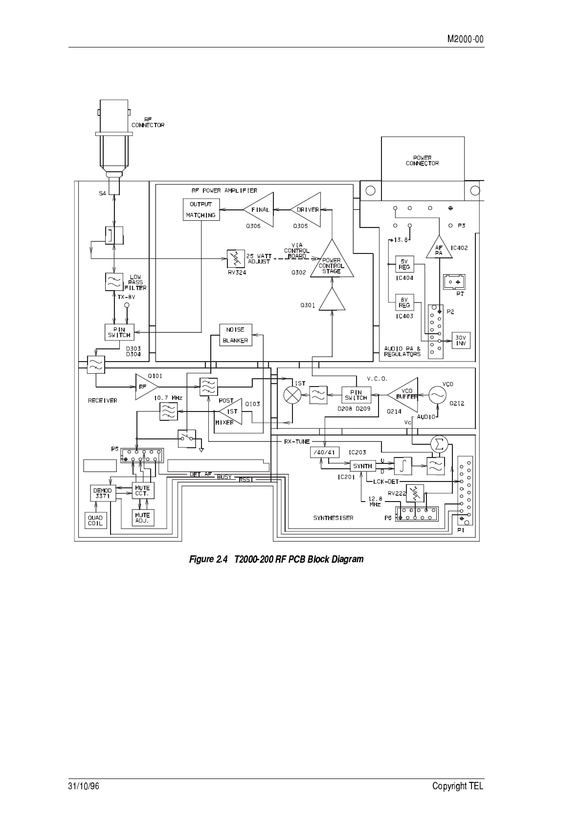
8/
8. 111113)6
8.8 11111#
The incoming signal from the antenna via the PIN switch passes through a high pass fil-
ter to the RF amplifier, Q101. The 50Ω output from the amplifier is coupled to a varicap
tuned triplet that provides the spurious response rejection necessary for the first mixer.
An attenuator is provided at the output to allow for fine adjustment of the front end
gain.
The VCO output is fed to the first double balanced mixer via a low pass filter to reduce
harmonic content. The VCO signal is 10.7MHz above the RF signal and the first mixer
output (at 10.7MHz) feeds the first post-mixer buffer, Q103. The output of Q103 feeds
both a delay line and the noise blanker circuit.

80
L114 and L116 form a 50Ω delay line that provides the delay necessary for the noise
blanker to detect and clamp noise pulses and also provides a high impedance point for
the signal to be clamped.
The 10.7MHz output feeds the plug-in IF PCB through R128, R129 and R132 which pro-
vide the attenuation equivalent to the second mixer of the T2000-300, T2000-400, T2000-
500 or T2000-600.
Each sub-block within the front end has been designed with 50Ω terminations for ease
of testing and fault finding.
8.8 11111'<#
The VCO output from the PIN switch is amplified to 500mW by a two stage broad band
exciter (Q301 and Q302) with approximately 2ldB of gain. Q301 is operating into com-
pression to prevent changes in VCO drive affecting output power. This output power is
controlled by varying the collector voltage on Q302, via Q303, Q304 and the feedback
loop from the PA. The power settings (maximum, high and low) are under microproces-
sor control and are set for each channel by programming. R308A, R308, R309 and R310
provide approximately 1dB of attenuation and isolation between the exciter and power
amplifier.
8.8 111117!&
The 500mW exciter output is amplified to 30W by Q305 and Q306. The T2000-200 power
amplifier has no tuning, and when the output power is set to 25W the variation across
the 22MHz switching range should be less than ±2W.
The high level RF signal passes via the Tx/Rx PIN switch, the low pass filter and the
directional coupler to the antenna connector. The power level is sensed by D301 on the
directional coupler and this voltage is fed back to the power control operational ampli-
fier via RV324. RV324 on the RF PCB sets the high power and RV507 on the logic PCB
will adjust the low power.
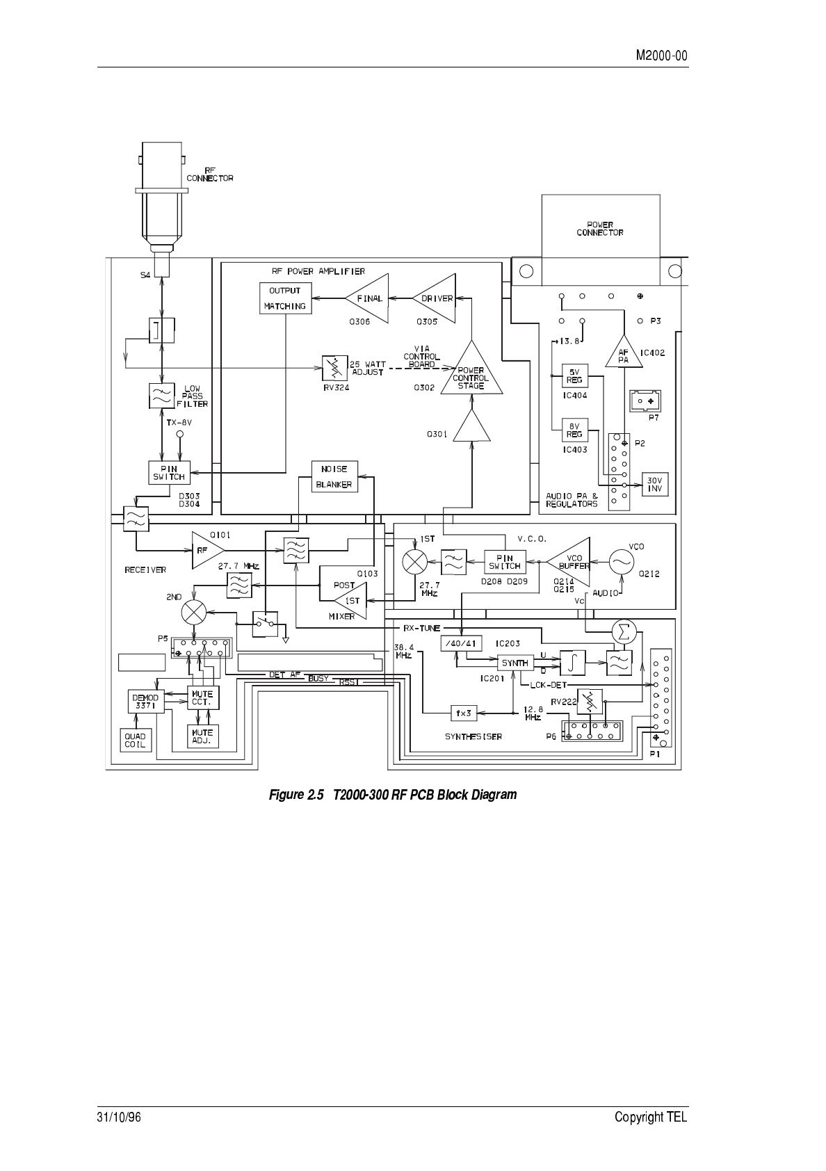
81
8/ 111 113)6
8/8 111 11#
The incoming signal from the antenna via the PIN switch passes through a high pass fil-
ter to the RF amplifier, Q101. The 50Ω output from the amplifier is coupled to a varicap
tuned triplet which provides the spurious response rejection necessary for the first
mixer. An attenuator is provided at the output to allow for fine adjustment of the front
end gain.
The VCO output is fed to the first double balanced mixer via a low pass filter to reduce
harmonic content. The VCO signal is 27.7MHz above the RF signal and the first mixer
output (at 27.7MHz) feeds the first post-mixer buffer, Q103. The output of Q103 feeds
both a delay line and the noise blanker circuit.

8
L114 and L116 form a 50Ω delay line which provides the spurious response rejection
necessary for the second mixer. L114 and L116 also provide the delay necessary for the
noise blanker to detect and clamp noise pulses. The local oscillator signal of 38.4MHz
for the second double balanced mixer is provided by the l2.8MHz reference via a tripler
circuit, and the 10.7MHz output feeds the plug-in IF PCB.
Each sub-block within the front end has been designed with 50Ω terminations for ease
of testing and fault finding.
8/8 111 11'<#
The VCO output from the PIN switch is amplified to 1W by a two stage broad band
exciter (Q301 and Q302) with approximately 22dB of gain. Q301 is operating into com-
pression to prevent changes in VCO drive affecting output power.
This output power is controlled by varying the collector voltage on Q302, via Q303,
Q304 and the feedback loop from the PA. The power settings (maximum, high and low)
are under microprocessor control and are set for each channel by programming.
R308, R309, R310 and R313 form a 2.7dB attenuator, reducing the output to approxi-
mately 550mW and also providing good isolation between the exciter and PA.
8/8 111 117!&
The 550mW exciter output is amplified to 30W by Q305 and Q306. Q305 has a small
amount of bias applied (via R319, D302, R322 and R315) to provide stability at low
power levels.
The T2000-300 power amplifier has no tuning, and when the output power is set to 25W
the variation across the 38MHz switching range should be less than ±2W.
The high level RF signal passes via the Tx/Rx PIN switch, the low pass filter and direc-
tional coupler to the antenna connector. The power level is sensed by D301 on the direc-
tional coupler and this voltage is fed back to the power control operational amplifier via
RV324. RV324 on the RF PCB sets the high power and RV507 on the logic PCB will
adjust the low power.
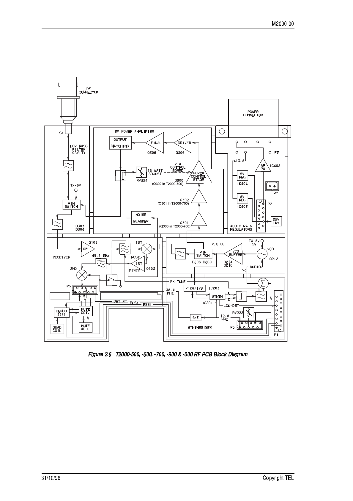
8
80 111+11:111-11:111.11:01141113
)6
808 111+11:-11:.11:0114111#
The incoming signal from the antenna via the PIN switch passes through a high pass fil-
ter to the RF amplifier, Q101. The 50Ω output from the amplifier is coupled to a varicap
tuned triplet which provides the spurious response rejection necessary for the first
mixer. An attenuator is provided at the output to allow for fine adjustment of the front
end gain.

8
The VCO output is fed to the first double balanced mixer via a low pass filter to reduce
harmonic content. The VCO signal is 49.lMHz below the RF signal and the first mixer
output (at 49.lMHz) feeds the first post-mixer buffer, Q103. The output of Q103 feeds
both a delay line and the noise blanker circuit.
L114 and L116 form a 50Ω delay line which provides the spurious response rejection
necessary for the second mixer. L114 and L116 also provide the delay necessary for the
noise blanker to detect and clamp noise pulses. The local oscillator signal of 38.4MHz
for the second double balanced mixer is provided by the 12.8MHz reference via a tripler
circuit, and the 10.7MHz output feeds the plug-in IF PCB. Each sub-block within the
front end has been designed with 50Ω terminations for ease of testing and fault finding.
808 111+11:-11:.110114111'<#
The VCO output from the PIN switch is amplified to 2W by a three stage broad band
exciter (Q300, Q301 and Q302) with approximately 28dB of gain. The first stage (Q301 in
the T2000-500/600, and Q300 in the T2000-700) operates into compression to prevent
changes in VCO drive affecting output power.
This output power is controlled by varying the collector voltage on Q300, via Q303,
Q304 and the feedback loop from the PA. The power settings (maximum, high and low)
are under microprocessor control and are set for each channel by programming.
808 111+11:-11:.11:01141117!&
The 2W exciter output is amplified to 30W by Q305 and Q306. The T2000-500/600/700
power amplifier has no tuning, and when the output power is set to 25W the variation
across the switching range should be less than ±2W.
The high level RF signal passes via the directional coupler, the Tx/Rx PIN switch and
the low pass filter to the antenna connector. The power level is sensed by D301 on the
directional coupler and this voltage is fed back to the power control operational ampli-
fier via RV324. RV324 on the RF PCB sets the high power and RV507 on the logic PCB
will adjust the low power.
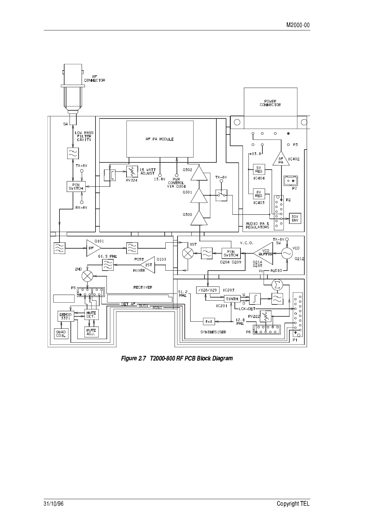
8"
81 111/113)6
818 111/11#
The incoming signal from the antenna via the PIN switch passes through a band pass
filter to the RF amplifier, Q101. The 50Ω output from the amplifier is coupled to a sec-
ond band pass filter, and these two filters provide the spurious response rejection neces-
sary for the first mixer. An attenuator is provided at the output to allow for fine
adjustment of the front end gain.
The VCO output is fed to the first double balanced mixer via a low pass filter to reduce
harmonic content. The VCO signal is 61.9MHz below the RF signal and the first mixer
output (at 61.9MHz) feeds the first post-mixer buffer, Q103. The output of Q103 feeds a
band pass filter.

8+
L114 and L116 form a 50Ω band pass filter which provides the spurious response rejec-
tion necessary for the second mixer. The local oscillator signal of 51.2MHz for the sec-
ond double balanced mixer is provided by the 12.8MHz reference via a times 4
multiplier circuit, and the 10.7MHz output feeds the plug-in IF PCB.
Each sub-block within the front end has been designed with 50Ω terminations for ease
of testing and fault finding.
818 111/11'<#
The VCO output from the PIN switch is amplified to 0.5W by a three stage broad band
exciter (Q300, Q301 and Q302) with approximately 21dB of gain. Q300 is operating into
compression to prevent changes in VCO drive affecting output power.
This output power is controlled by varying the voltage on IC405 pin2, via Q303, Q304
and the feedback loop from the PA. The power settings (maximum, high and low) are
under microprocessor control and are set for each channel by programming.
818 111/117!&
The 0.5W exciter output is amplified to 20W by IC405. The T2000-800 power amplifier
has no tuning, and when the output power is set to 15W the variation across the 70MHz
switching range should be less than ±1W.
The high level RF signal passes via the directional coupler, the Tx/Rx PIN switch and
the low pass filter to the antenna connector. The power level is sensed by D301 on the
directional coupler and this voltage is fed back to the power control operational ampli-
fier via RV324. RV324 on the RF PCB sets the high power and RV507 on the logic PCB
will adjust the low power.

8-
8 )
The primary task of the control section in the T2000 is to control the state of the radio at
all times, based both on user input, and activity of the internal circuitry. To achieve this,
the control section monitors the radio’s operation and responds to any changes with
various control signals.
The input shift registers are read by the microprocessor approximately 100 times per
second. The output shift registers are updated only when a control signal is required to
change, and the miscellaneous I/O is continually scanned.
In the majority of cases, a control output will change only in response to an input stimu-
lus, e.g. a control head key being pressed, receiver busy, etc. Some outputs may be
affected by more than one input or a sequence of events; this is particularly so in the
case of the mute gate control line. Its operation may be affected by a number of external
conditions and even some generated in the microprocessor.
For operation of the T2000 Series II control heads, refer to Figures 2.8 to 2.10.
88 1141+=)1+,#)6
Transmitter speech from the microphone is preamplified and fed into an automatic level
control circuit which also has two mute facilities (one for options and one for the micro-
processor). The speech is pre-emphasised and high pass filtered to reduce CTCSS com-
ponents, then passes via the RF PCB to the limiter on the TCXO/Tx audio PCB.
DCS/CTCSS signals are generated by the microprocessor and are filtered by a low pass
filter before being passed to the level potentiometer on the TCXO/Tx audio PCB. A five
tone Selcall module is available which is directly interfaced to the microprocessor.
Selcall tones are fed to the limiter on the TCXO/Tx audio PCB.
Receiver audio from the IF PCB passes through a low pass filter where it is split into sig-
nalling and speech paths. Five tone signals are coupled to the five tone module. DCS/
CTCSS passes through a low pass filter and limiter before arriving at the microproces-
sor. Speech is de-emphasised and passed through one or two high pass filters, depend-
ing on the signalling used. Processed speech passes through the mute to an amplifier
where speech and progress tones are summed. The signal then passes via the volume
control to the audio power amplifier on the RF PCB.
8.
8/

80
88 11:1 ;:1"1:1+141-1=),#)6
Transmitter speech from the microphone is preamplified and fed into an automatic level
control circuit which also has three mute facilities (one for options and two for the
microprocessor). The speech is pre-emphasised and high pass filtered to reduce CTCSS
components. The speech passes via the RF PCB to the limiter on the TCXO/Tx audio
PCB.
The FFSK modem tones pass through a level potentiometer before being fed to the lim-
iter on the TCXO/Tx audio PCB. DCS/CTCSS signals are generated by the microproces-
sor and are filtered by a low pass filter before being passed to the level potentiometer on
the TCXO/Tx audio PCB.
Five tone Selcall and DTMF modules are both available to directly interface to the
microprocessor. Selcall tones are fed to the limiter on the TCXO/Tx audio PCB and
DTMF tones are summed at the automatic level control.
Receiver audio from the IF PCB passes through a low pass filter where it is split into sig-
nalling and speech paths. Five tone signals are coupled to the five tone module. DCS/
CTCSS passes through a low pass filter and limiter before arriving at the microproces-
sor. FFSK modem signals pass through a buffer amplifier before the modem input.
Speech is de-emphasised and passed through one or two high pass filters, depending on
what signalling is used. Processed speech passes through the mute to an amplifier
where speech and progress tones are summed. The signal then passes via the volume
control to the audio power amplifier, on the RF PCB.

81
8
This Section provides information necessary for servicing T2000 Series II radios, and
covers the following topics:
Section Title Page
3.1 Servicing Precautions 3.2
3.1.1
3.1.2
3.1.3
3.1.4
3.1.5
Caution: Accidental Transmit
Caution: Antenna Loading
Caution: Beryllium Oxide & Power Transistors
Caution: CMOS Devices
Caution: Screw Head Types
3.2
3.2
3.2
3.2
3.3
3.2 Disassembly Instructions 3.5
3.2.1
3.2.2
3.2.3
3.2.3.1
3.2.3.2
3.2.4
3.2.4.1
3.2.4.2
3.2.5
3.2.6
To Gain Access To The Logic PCB
To Remove The Bottom Cover And Microprocessor Shield
To Detach The Control Head
Locally Mounted Models
Remotely Mounted Models
To Disassemble The Control Head
T2010, T2015, T203X & T2060 Radios
T2020, T2040 & T2050 Radios
To Detach The EMC Filter PCB
To Remote A Locally Mounted T2020, T2040 & T2050
3.5
3.5
3.6
3.6
3.6
3.7
3.7
3.9
3.11
3.11
3.3 Power Amplifier - Special Instructions 3.12
3.3.1
3.3.2 To Replace PA Transistors
To Remove Case Mica Capacitors 3.12
3.12
3.4 Repair 3.13
3.4.1
3.4.1.1
3.4.1.2
3.4.1.3
3.4.1.4
3.4.2
3.4.2.1
3.4.2.2
Surface Mount Devices
Surface Mount Device (SMD) Precautions
Servicing Equipment Required
Removal & Replacement Of SMD Components
Common Causes Of SMD Failure
Leaded Component Removal
Desoldering Iron Method
Component Cutting Method
3.13
3.13
3.13
3.15
3.17
3.17
3.17
3.18
3.5 Programming 3.18
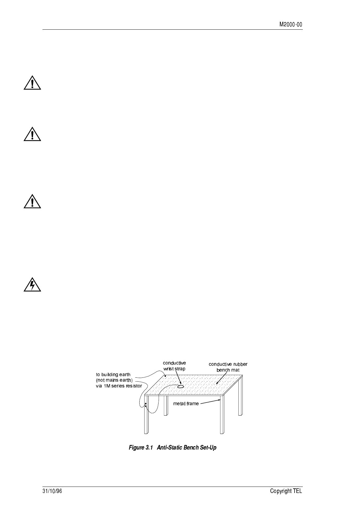
8
8 ##
88 )!##
Under certain circumstances the microprocessor can key the transmitter. Ensure that all
instruments are protected from accidental transmit at all times.
88 )!,
The equipment has been designed to operate with a 50Ω termination impedance, but
will tolerate a wide range of antenna loading conditions. However, it is strongly recom-
mended that the transmitter is not operated in the absence of a suitable load. Failure to
observe this precaution may result in damage to the transmitter power output stage.
88 )6*<47
The RF power transistors in the T2000 all contain some beryllium oxide. This substance,
while perfectly harmless in its normal solid form, can become a severe health hazard
when it has been reduced to dust.
For this reason the RF power transistors should not be scratched, mutilated, filed,
machined, or physically damaged in any way that can produce dust particles.
88" ))*#
This equipment contains CMOS Devices which are susceptible to damage from static
charges. Care when handling these devices is essential. For correct handling procedures
refer to manufacturers’ data books covering CMOS devices, e.g. Philips Data Handbook
Covering CMOS Devices; Motorola CMOS Data Book Section 5 (Handling Procedures),
etc.
The following diagram shows a typical anti-static bench set-up.
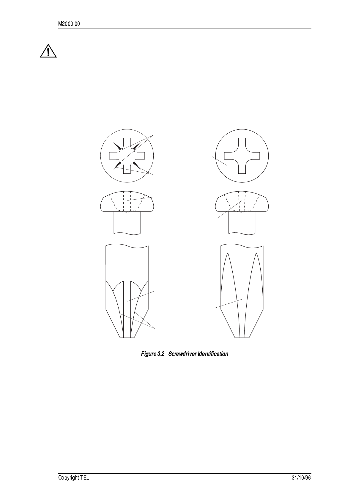
8
88+ )#7=&
Pozidriv screws are the preferred standard on all T2000 series equipment. Pozidriv No.
1 and 2 screwdrivers will fit all pozidriv screws used in the T2000: Philips cross-head
screwdrivers are not satisfactory for use on these screws.
The following diagram identifies the differences between Philips and Pozidriv screw-
drivers.
The diagrams on the following pages show the types of screws used in the T2000
Series II radios, their locations and torque specifications.
driving flutes with
parallel sides
driving flutes with
tapered sides
Pozidriv Philips
internal notches
"star" markings
between slots
no special markings
slots with parallel sides
slots with tapered sides
ridges between
driving flutes
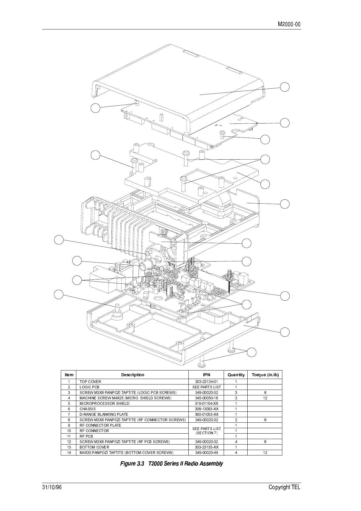
8"
7
13
14
9
12
11
6
1
2
3
3
4
4
5
8
10
14
12

8+
8 $#
To carry out alignment it is necessary to remove only the top cover (1) and
logic PCB retaining screws (3). It is essential that the bottom cover (13) and
microprocessor shield (5) with its three retaining screws (4) are torqued
down as specified in Figure 3.3.
Various electronic components within the radio can be damaged by elec-
trostatic discharge. A properly grounded earth mat and wrist strap should
be used at all times (refer to Section 3.1.4).
88 2!##,#)6
Refer to Figure 3.3.
Remove the top cover (1) by unscrewing the four bottom cover screws (14).
Remove the three logic PCB retaining screws (3).
It should now be possible to open out the logic PCB (2), giving access to both sides
of the logic PCB, and access to the RF PCB (11) tuning points, audio, plug-in
TCXO PCB and loop filter components.
88 6)!#&#
Refer to Figure 3.3.
Remove the top cover and logic PCB screws as instructed in Section 3.2.1, then
remove the three microprocessor shield retaining screws (4).
Remove the screw securing the earthing wire from the control head to the micro-
processor shield.
It should now be possible to lift off the microprocessor shield (5) and the bottom
cover (13).
This will give access to both sides of the RF PCB and IF PCBs, and enable the con-
trol head to be removed.

8-
88 #)=
88 8 ,#
Remove all covers, as instructed in Section 3.2.2.
Unplug the loom running between the control head and the logic PCB.
In EMC model radios, the loom connects to a Micromatch connector on the
EMC filter PCB (refer to Section 3.2.5).
88 8
Remove the four screws on the front of the radio dummy front panel. This will
give access to the control head loom, which can now be unplugged.
In EMC model radios, the loom connects to a Micromatch connector on the
EMC filter PCB (refer to Section 3.2.5).
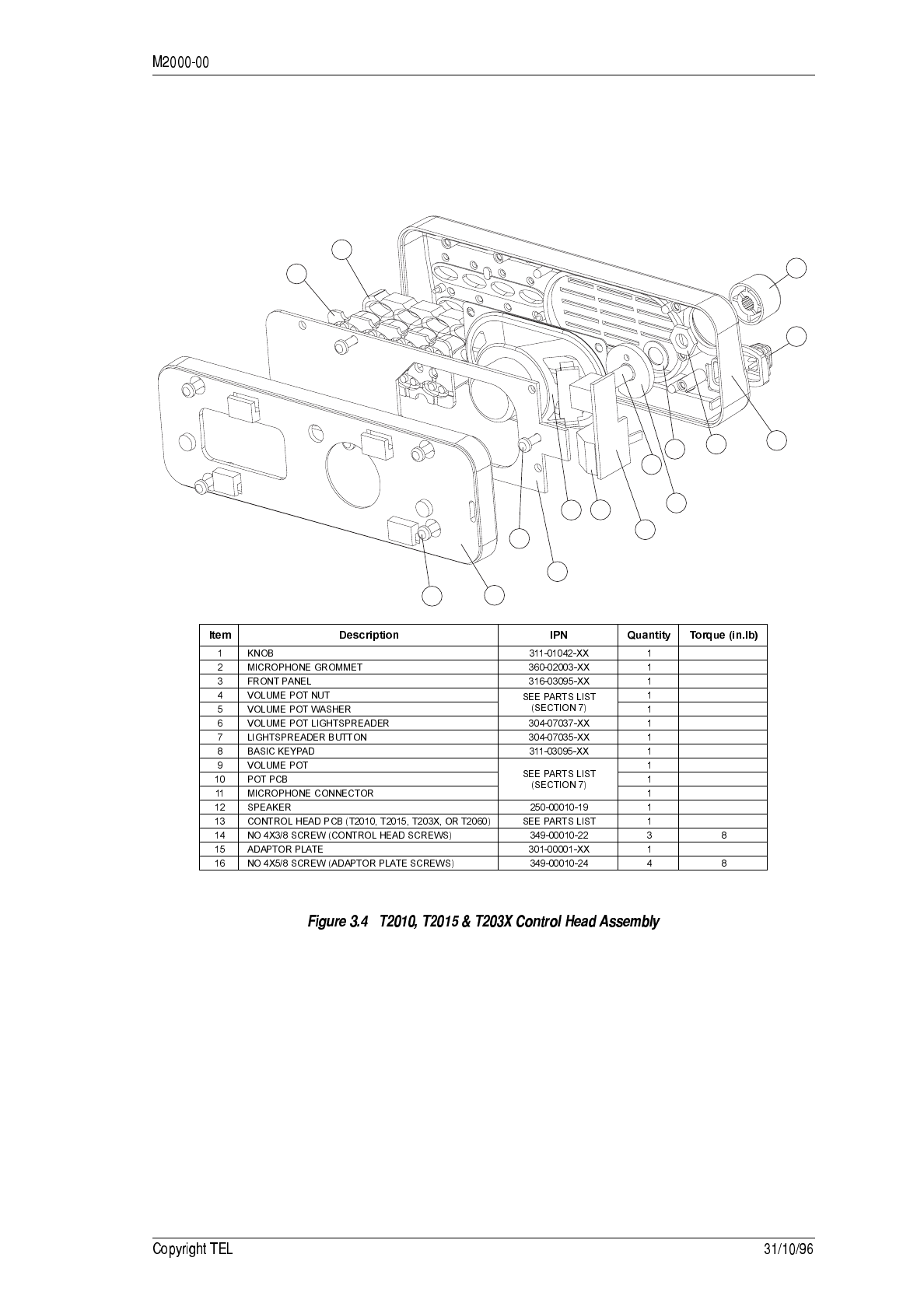
8.
88" )=
88"8 11:1+:1 ;41-1
Refer to Figure 3.4.
Remove the control head from the main chassis, as instructed in Section 3.2.3.
Remove the four adaptor plate retaining screws (16).
Remove the control head PCB retaining screws (14).
7
8
2
4
5
6
9
12
10
13
14
11
15
16
3
1
8/
The screws used in the control head are No. 4 Plastites, and should not be con-
fused with the M3 screws used elsewhere. When being replaced, the No. 4 Plas-
tite screws must be tightened to a torque of 8in.lb (0.9Nm).
With the control head face down, gently remove the PCB (13), along with the key-
pad (8) and lightspreader (7).
Do not disturb the positioning or height of the LEDs, as this is critical for reas-
sembly.
Remove the speaker by carefully removing the four speaker retaining spire nuts.
Remove of the volume knob (1) and volume pot nut (5) to access the volume knob
light spreader (6).
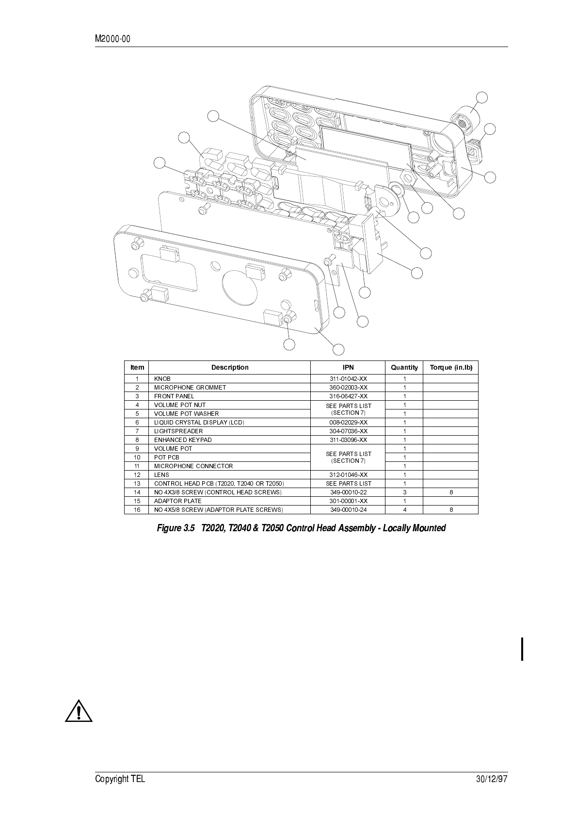
80
88"8 11:1"141+1
Refer to Figure 3.5 and Figure 3.6.
Remove the control head from the main chassis, as instructed in Section 3.2.3.
Remove the four adaptor plate/remote back panel retaining screws (16). Remote
mounted models also have two captive nuts (17) fitted in the back cover.
EMC model radios have 4 ESD plugs fitted over the remote back panel screws.
These will need to be removed to access the remote back panel screws.
Remove the control head PCB retaining screws (14).
The screws used in the control head are No. 4 Plastites, and should not be con-
fused with the M3 screws used elsewhere. When being replaced, the No. 4 Plas-
tite screws must be tightened to a torque of 8in.lb (0.9Nm).
4
10
9
6
512
3
2
1
15
7
8
16
11
13
14
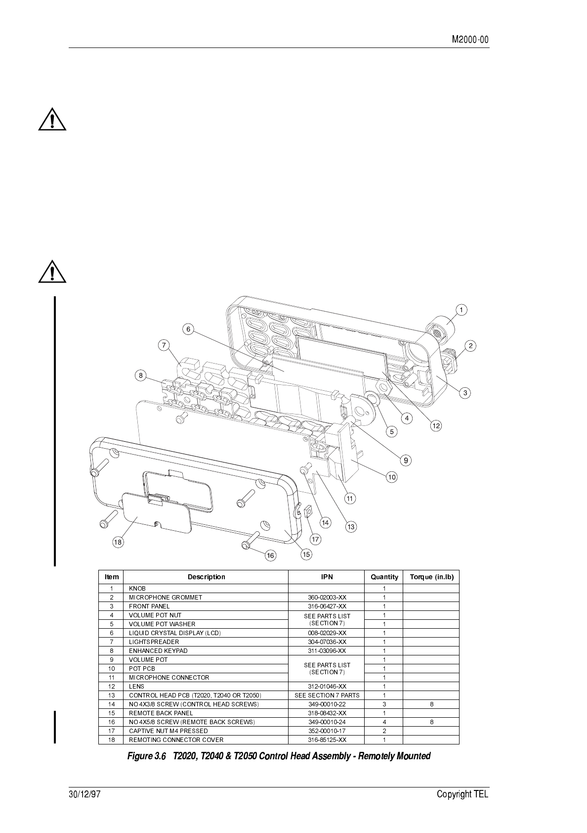
81
With the control head face down, gently remove the PCB (13), along with the key-
pad (8) and lightspreader (7).
Do not disturb the positioning or height of the LEDs, as this is critical for reas-
sembly.
Carefully remove the LCD (6) and lens (12).
Lay the front panel (3) on a horizontal surface, with the light spreader (7) in place.
Remove the volume knob (1) and volume knob nut (5) to access the lightspreader
and keypad (8).
Before reassembly, the LCD and PCB edge connectors should be wiped with alco-
hol.
Take care to ensure the alcohol does not come in contact with the coating on the
light spreader, as this will dissolve on contact with alcohol.
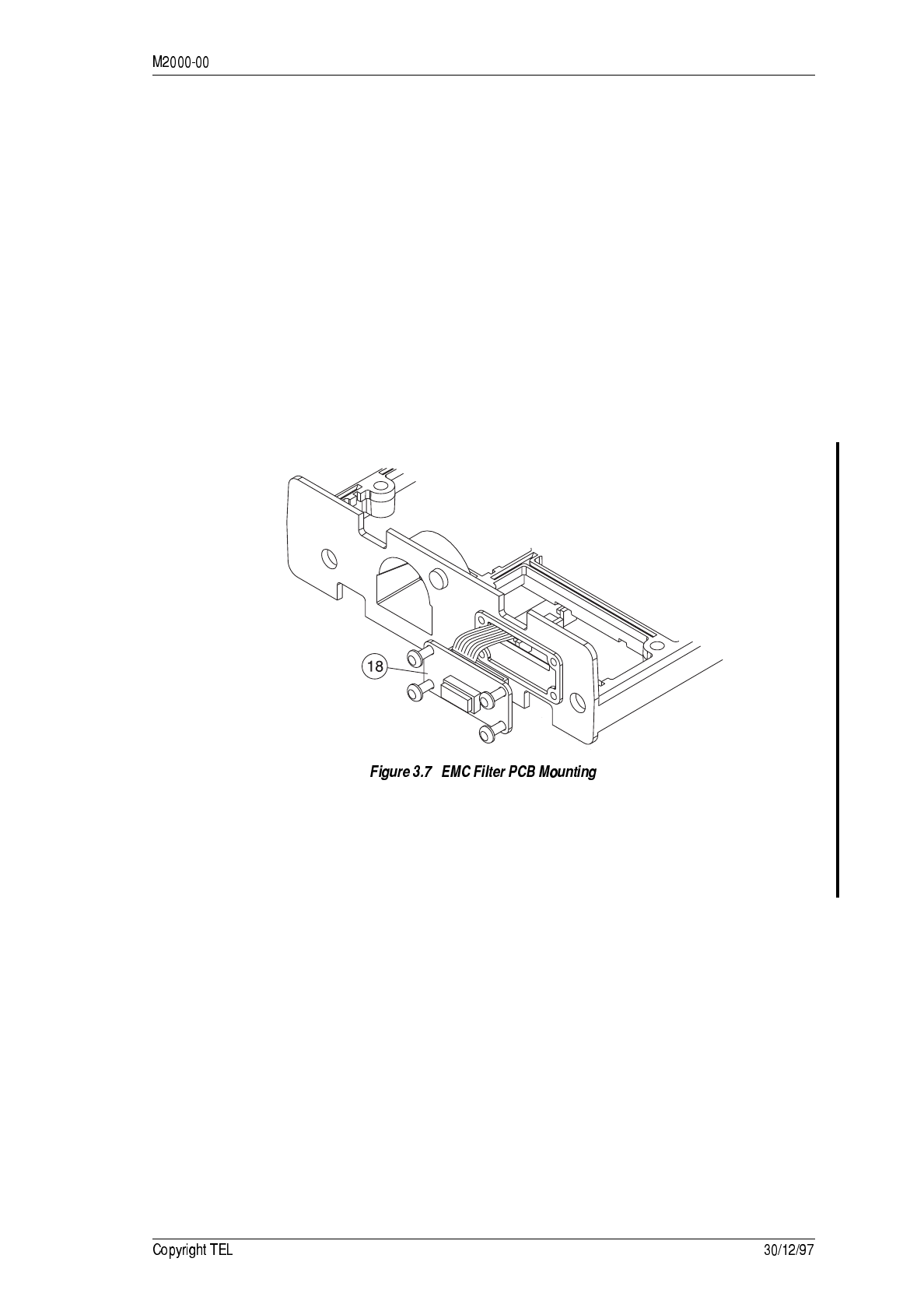
8
88+ #')3)6
Refer to Figure 3.7.
Remove the top cover and open the logic PCB, as described in Section 3.2.1.
Remove the microprocessor shield and bottom cover, as described in Section 3.2.2.
The control head (locally mounted models) or dummy front panel (remotely
mounted models) can now be removed.
Unplug the loom running between the logic PCB and EMC filter PCB (18).
Unplug the loom running between the EMC filter PCB and the control head.
Remove the 4 EMC filter PCB retaining screws. The EMC filter PCB can now be
lifted from the chassis.
88- !,#11:1"141+1
Refer to Section 8.16, “T2000-A03/-A04/-A16 Remote Loom Kits”.
8
8 7!&&#$#
As the location of certain components in the PA is critical to performance,
it is important that any components removed or disturbed are refitted in
exactly the same location.
8 8 &#!
Desolder the tabs by heating them with a soldering iron, then lifting them up
towards the transistor with a thin stainless steel spike or screwdriver.
Unscrew the transistor mounting stud nut or screws and remove the transistor.
Trim the tabs of the replacement to make them similar to the faulty item, then
lightly tin the underside of the tabs.
Apply a thin layer of heatsink compound to the underside of the transistor.
Screw the transistor tightly to the heatsink then solder the tabs.
Do not solder the tabs before tightening the screws or nut, as this will fracture
the device.
8 8 )#)&#
Apply a heavy duty soldering iron to the top of the capacitor case.
When the solder is molten, ease the capacitor away from the PCB with a thin
stainless steel spike or screwdriver.

8
8" &
8"8 ##
Surface mount devices require special storage, handling, removal and
replacement techniques. This equipment should be serviced only by an
approved Tait Dealer or Service Centre equipped with the necessary facil-
ities. Repairs attempted with incorrect equipment or by untrained person-
nel may result in permanent damage. If in doubt, contact Tait Electronics
Ltd or your nearest Tait Branch or Subsidiary.
8"88 ##>?#
The following points must be observed when servicing SMDs:
• Carry out all servicing in a static safe work area (refer to Figure 3.1).
• Always observe static precautions when handling or carrying SMDs. Carry in foil,
anti static bags or in trays and anti-static tubes for fine pitch ICs.
• Use appropriate tools when working with SMDs (refer to 3.4.1.2).
• Do not use soldering irons on surface mount capacitors, resistors, SOIC and SOT
components.
• Use new solder when replacing SMDs.
• Use the correct amount of solder (refer to Figure 3.9).
• Never reuse old SMDs.
• Do not use SMDs that have been dropped.
8"88 #'(&(
• Hot air tool or heat gun: adjustable temperature is required and a regulated hot air
blower. The nozzle is changed according to the size of the SMDs.
• Weller Pyropen®: this is a butane hot air tool, and is hotter than a heat gun. For use
only for resistors, capacitors and SOTs.
• Solder paste dispenser or syringe: for SMD placement.
• Tweezers: for use when handling SMDs.
• Solderwick: for removing solder on SMD pads or for removing excess solder or
bridging on multi-leg components.
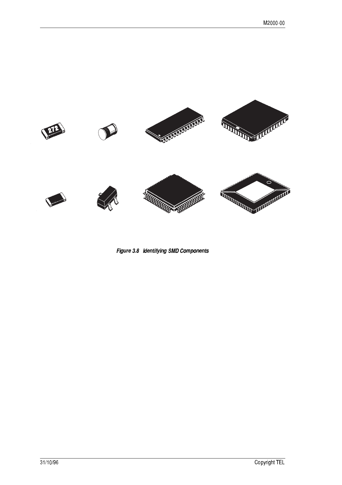
8"
• Soldering iron: for use on electrolytic capacitors and plastic coated devices that may
be damaged by a heat gun.
• Microscope: for individual SMD inspection and for SMD replacement.
Use the following diagram to identify types of SMD components.
2
72
2
72
RESISTOR MELF SOIC PLCC
LCCC
QFP
SOT
CAPACITOR

8+
8"88 4&#*)&
Refer to Figure 3.9.
(a) Capacitors, Resistors, MELF & SOT
Hold the nozzle of the hot air tool above the component and keep it moving to
ensure that the PCB is not damaged.
Remove the SMD and clean away any glue using the hot air tool and a pair of
tweezers.
Remove any excess solder from the pads using solderwick.
Deposit a small amount of solder paste on the pads using the solder paste dis-
penser or syringe.
Apply heat evenly to both sides of the device using the hot air gun or Weller Pyro-
pen®, until all the paste has reflowed. As this happens, the device will self-align
on the pads. If necessary, use tweezers to prevent the SMD from moving while
heat is being applied.
(b) SOIC, VSO, QFP, LCCC & PLCC
Hold the nozzle of the hot air tool on top of the leads and keep it moving to ensure
that the PCB is not damaged. A hot air tool with the correct size nozzle must be
used.
After a few seconds heating, use a very gentle twisting motion to allow the device
to move away from its associated pads.
Carefully remove all excess solder from the pads using a soldering iron and sol-
derwick.
Apply an even amount of solder paste along the full length of the pads, using flux
where necessary.
Align the device accurately on the pads and apply a slight pressure with the
tweezers to hold in place.
Hold the heat nozzle at an angle and move it slowly along the leads, ensuring that
the paste reflows properly.
If any fine bridges occur, use a spike or solderwick to clear. If this is necessary,
apply more solder paste before using the hot air gun again.
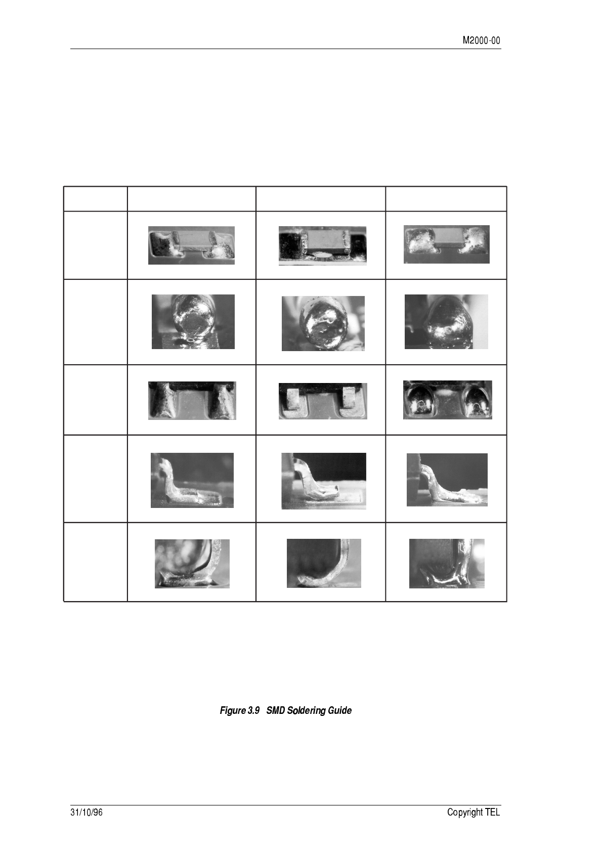
8-
capacitor
& resistor
MELF
SOT
SOIC
(gull leads)
PLCC
(J leads)
excess solder
adaquate solder insufficient solder

8.
8"88" ))*3
(a) Cracked SMD
Most often occurs with capacitors, caused by:
• Thermal shock: if the SMD is heated too rapidly either it will crack or internal
seals will be lost, resulting in premature failure.
• In-service temperature changes that cause invisible micro-cracks. These start
at or just under the end termination and will spread throughout the device
over a long period of time.
(b) Solder Joint Failure
• Stress causing flexing of the PCB leads to a cracked joint.
• Excessive or too little solder results in a poor quality joint.
• Various soldering process defects such as solder balling, device misalignment,
solder bridging and glue defects.
(c) Static Electricity Damage
If static electricity damage is suspected, remove and replace the component.
8"8 ,)&
Whenever components are removed from or fitted to the PCB, care must be taken to
avoid damage to the track. The two satisfactory methods of removing components from
PTH PCBs are detailed below.
8"88 $
Use a desoldering station, e.g. Philips SBC 314 or Pace MBT-100E for this method.
Place the tip over the lead and, as the solder starts to melt, move the tip with a cir-
cular motion.
Start the suction and continue the movement until 3 or 4 circles have been com-
pleted.
Remove the tip while continuing suction to ensure that all solder is removed from
the joint, then stop the suction.
Before pulling the lead out, ensure it is not stuck to the plating. If the lead is still
not free, resolder the joint and try again.
The desoldering iron does not usually have enough heat to desolder leads from
the ground plane. Additional heat may be applied by holding a soldering iron on
the tip of the desoldering iron (this may require a helper).

8/
8"88 )&)
Cut the leads on the component side of the PCB.
Heat the solder joint sufficiently to allow easy removal of the lead by drawing it
out from the component side: do not use undue force.
Fill the hole with solder and then clear with solderwick.
8+
Refer to the T2000 programming manual supplied with the T2000 programming kit, and
Section 9 of this manual.
"8
" 3#
This Section details test procedures will confirm that the T2000 has been adjusted cor-
rectly and is fully operational.
The following topics are covered:
Section Title Page
4.1 Test Equipment Required 4.2
4.2 Connecting The Radio 4.3
4.3 Trunked Radios 4.4
4.3.1 Trunking System Check 4.4
4.4 Receiver Performance Tests 4.5
4.4.1
4.4.2
4.4.3
4.4.4
4.4.5
4.4.6
4.4.7
4.4.8
To Check The Squelch Operation
To Check The Squelch Ratio
To Check The Audio Output Level And Distortion
To Check The Sinad Sensitivity
To Check The Signal+Noise To Noise Ratio
To Check The Ultimate Signal To Noise Ratio
RSSI
To Check The Operation Of The Noise Blanker
4.5
4.5
4.6
4.6
4.7
4.7
4.7
4.8
4.5 Transmitter Performance Tests 4.9
4.5.1
4.5.1.1
4.5.1.2
4.5.1.3
4.5.2
4.5.2.1
4.5.2.2
4.5.3
Audio Processor
To Check The Limiter Circuit Operation
To Check The Audio ALC Operation
To Check The Gain Of The Audio Processor
Modulation Characteristics
To Check The Above Limiting Response
To Check The Below Limiting Response
To Check The RF Power Control Circuit
4.9
4.9
4.9
4.10
4.10
4.10
4.10
4.11

"8
"8 '(&(
The following equipment is required for functional testing.
• Power supply cord, wired as shown in Section 8.3.
• Power supply adjustable between 9 & 16V DC, with a capacity of at least 8A.
• VHF or UHF signal generator: good quality FM 50Ω, usable from 0.1V (-127dBm) to
200mV (0dBm) pd (e.g. HP8640B, Marconi 2019).
• Frequency counter: 10Hz to 650MHz, 2ppm stability, with at least a 2s time base res-
olution (e.g. Opto).
• Audio signal generator: 600Ω output, -50 to 0dB level, fully adjustable, sine wave
output 10Hz to 100kHz (e.g. Trio 203, HP204C/D).
• FM deviation meter (e.g. Sayrosa 257 or 252), with the following specifications:
-low residual FM
-resolution down to a full scale of 1kHz and a minimum of 10kHz
-maximum positive and negative peak display
-15kHz low pass filter
-detected audio output facility.
When using with LTR or DCS, the deviation meter must have a good low fre-
quency response, to avoid incorrect deviation readings.
• Sinad meter or audio distortion analyser, 1kHz notch type (e.g. HP334A, HP339A or
Helper Instruments Sinadder).
• AC millivoltmeter (e.g. Trio VT-106).
• Digital multimeter (e.g. Fluke 75).
• 20MHz dual channel oscilloscope and X10 . X1 scope probes (e.g. Trio CS1022).
• RF power meter, 50Ω; RF detecting element 50W and 5W for appropriate frequency
ranges (e.g. Bird Meter 6154 or 611).
• RF power attenuator, 50Ω, total attenuation 30dB (e.g. Weinschel 40-40-33 30dB,
150W).
• Microphone test box (refer to Figure 4.1).
A multifunction test set may be used as long as it has the appropriate function to per-
form the calibration correctly e.g. Rhode & Schwarz CMS52 Radio Communications
Test Set, with a high stability oscillator.
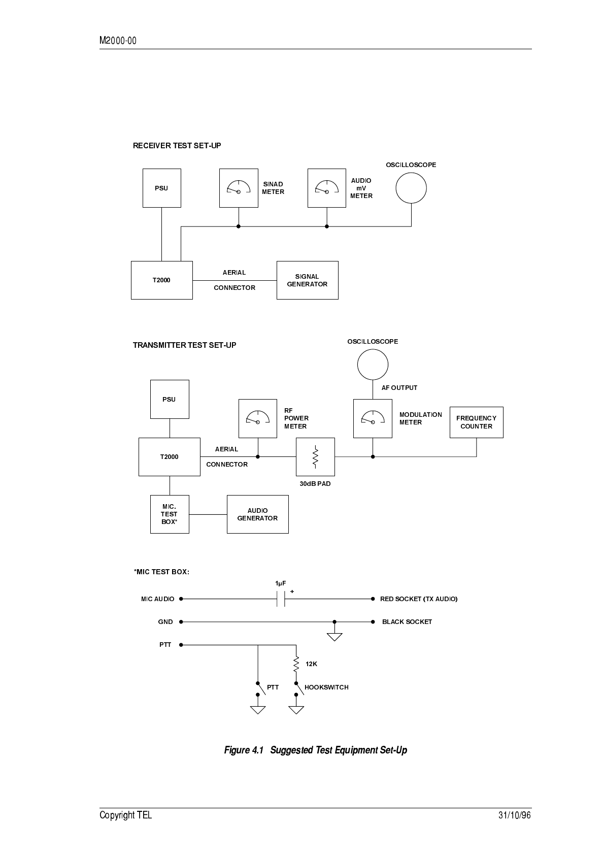
"8
"8 )#
The following diagram shows a suggested test equipment set-up.
"8"
"8 9
The ‘test’ facility enables T2000 trunked radios to emulate a multichannel radio, using
the frequencies reserved for trunking.
For a description of how to put the radio in test mode, refer to Section 5.8, “Trunked
Radios: Test Mode”. Once the radio is in test mode, functional testing can be carried out
as described in Section 4.4 and Section 4.5.
When in test mode, connect the antenna socket to a dummy load to pre-
vent interference with trunking systems. Avoid testing on channels in use
locally.
"8 8 9)#9
Connect the radio to an antenna and switch on.
Check that the radio locks onto the system:
T203X radios: the LED illuminates.
T2040 radios: the annunciator will appear in the control head display.
The following parameters relating to the local trunking system base station must
be correctly programmed before the mobile will lock onto the system:
• Base station channel numbers and frequencies.
•Network ID.
• Zone and area field length.
• Base station control channel number in the hunt list.
• Valid acquisition authorisation code (for test purposes this can be set to ‘none’,
which allows total access).
Initiate a call to a known unit identity. For test purposes this can be your own
identity.
Check that:
• The radio beeps.
• A 0.5s ringing tone is sounded.
• The receiver unmutes.
• T203X: The LED illuminates.
• T2040: the annunciator comes on.

"8+
"8" ##
In this Section, deviation settings are given first for wide band, followed by settings for
medium band in brackets ( ) and settings for narrow band in square brackets [ ].
"8"8 )#9(#*&
Connect a sinad meter across the speaker terminals.
Connect an on-channel RF signal generator to the antenna input terminal.
Disable any signalling control in T2010 or T2020 models by using the monitor
function. The control head LED should now be active.
Reduce the signal generator output level to -127dBm, modulated to ±3kHz
(±2.4kHz) [±1.5kHz] deviation at 1kHz AF.
Increase the RF output level until the squelch gate just opens.
Check that the reading on the sinad meter is between 8 and 14dB.
Reduce the signal generator output and check that the squelch gate closes within
4dB of the original RF level.
"8"8 )#9(#
Set the signal generator output level to -47dBm, modulated to ±5kHz (±4kHz)
[±2.5kHz] deviation at 1kHz AF.
Replace the sinad meter with an audio millivoltmeter across the speaker termi-
nals.
Adjust the volume control to the onset of clipping.
Reduce the signal generator output level to -127dBm.
The fall in output is the ‘squelch ratio’, and this should be at least 70dB.
"8-
"8"8 )#9!*&,!
Connect an audio millivoltmeter and an oscilloscope across the speaker terminals.
Connect an on-channel RF signal generator to the antenna input socket, with the
output set to -107dBm (1V) modulated to ±5kHz (±4kHz) [±2.5kHz] deviation at
1kHz AF.
Set the volume control to the onset of clipping.
The receiver output should be 4.2Vrms across 4Ω at +13.8V supply.
Check the distortion with the aid of a distortion analyser connected across the
speaker terminals.
The distortion should not exceed 5%.
"8"8" )#9
Connect a sinad meter across the speaker terminals.
Connect the signal generator to the antenna input terminal.
Set the signal generator accurately on the receive frequency.
Set the modulation for ±3kHz (±2.4kHz) [±1.5kHz] deviation at 1kHz AF.
Increase the signal generator output until a 20dB sinad is reached.
Switch off the signal generator modulation.
Couple a 10.7MHz reference oscillator loosely into the receiver IF stage, tune the
signal generator for a zero beat, then uncouple the reference oscillator.
Set the signal generator deviation to ±3kHz (±2.4kHz) [±1.5kHz] at 1kHz AF.
The modulating frequency must match the notch of the sinad meter.
Set the signal generator output level to -127dBm.
Disable the squelch control circuitry using the key on the T2010,
T2015, T2020, T2050 or T2060, the key on the T203X, or “function
21” on the T2040. The LED should then flash.
Increase the signal generator output level until a sinad of 12dB is reached.
The signal generator output should not be greater than -117dBm and is typically
-119dBm.
Fn

"8.
"8"8+ )#9@AA
Set the signal generator output level to -107dBm modulated to ±5kHz (±4kHz)
[±2.5kHz] deviation at 1kHz AF.
Connect an audio millivoltmeter across the speaker terminals.
Set the volume control for a reading of 0.8V (0dBm) on a convenient scale on the
millivoltmeter.
Switch off the signal generator modulation.
Note the reading on the millivoltmeter.
The fall in reading when the modulation is switched off should typically be 30dB
(28dB) [25dB].
"8"8- )#9%A
A good quality RF signal generator with low residual FM must be used for this
check (e.g. HP8640B or 8656).
Set the signal generator to give an on-channel signal, modulated to ±5kHz
(±4kHz) [±2.5kHz] with a 1kHz tone.
Set the signal generator output level to -47dBm.
Connect an AC millivoltmeter across the speaker terminals.
Adjust the volume control for a reading of 0.8V (0dBm) on a convenient scale.
Turn off the signal generator modulation.
Note the reading on the millivoltmeter.
The fall in reading when the modulation is switched off should be at least 50dB
(48dB) [45dB].
"8"8. $
Set the signal generator to give an unmodulated signal at an output level of
-120dBm.
Increase the input level in 10dB steps over the 50dB dynamic range and monitor
the RSSI output on pin 15 of S14 (logic PCB).
Ensure the output varies approximately 540mV/10dB over the dynamic range.

"8/
"8"8/ )#9*&*A69
Connect an ignition noise simulator and an RF signal generator to the receiver
antenna input.
Set the signal generator modulation for ±3kHz (±2.4kHz) [±1.5kHz] deviation at
1kHz AF.
Set the signal generator output level to give a 20dB sinad.
Listen to the receiver output and check the operation of the noise blanker by tem-
porarily short circuiting R135 on the RF PCB to ground, thus disabling the noise
blanker.
The noise blanker should give a marked reduction in noise over a wide range of
noise input amplitudes.

"80
"8+ #
In this Section, deviation settings are given first for wide band, followed by settings for
medium band in brackets ( ) and settings for narrow band in square brackets [ ].
"8+8 !#
"8+88 )#9,)#*&
Connect an oscilloscope to monitor the waveform at TSP901 (TCXO PCB).
Plug the microphone test lead into the control head microphone input socket.
Apply a 1kHz sine wave.
Slowly increase the sine wave output level until the waveform begins to distort
(squaring), indicating that limiting has commenced.
Any further increase in sine wave output level should not increase the amplitude
of the waveform.
"8+88 )#9!!,)*&
Connect an oscilloscope to monitor the waveform at TP606 (logic PCB).
Apply a 1kHz sine wave.
Connect an EVM to the junction of R667 and C639.
Increase the sine wave output level to 10dB above the limiting level, as described
in Section 4.5.1.1.
Note the amplitude on the oscilloscope, then increase the output level by another
10dB.
Check that the amplitude of the waveform does not increase or distort signifi-
cantly.
The EVM should show a positive DC reading.

"81
"8+88 )#92*!#
Connect the T2000 antenna output via a 30dB attenuator to a modulation meter.
Plug the microphone test lead into the control head microphone input socket.
Apply a 1kHz sine wave and adjust the output level to give a 3kHz (2.4kHz)
[1.5kHz] deviation reading on the modulation meter.
Connect a millivoltmeter across the input of the microphone test box and check
for a reading of approximately 1mVrms on the millivoltmeter.
The audio processor gain must be checked at a level below that at which the
audio ALC or limiting are influencing the measurements.
"8+8 )##
"8+88 )#9!,&
Connect the T2000 antenna output via a 30dB attenuator to a modulation meter.
Plug the microphone test lead into the control head microphone input socket.
Apply a 1kHz sine wave and increase the output level to 20dB above the limiting
level, as described in Section 4.5.1.1.
Vary the frequency of the sine wave generator between 0.3 and 5kHz.
Note the reading on the modulation meter.
The deviation should not exceed ±5kHz (±4kHz) [±2.5kHz].
Between 450Hz and 3kHz (3kHz) [2.55kHz] the deviation should be within 4dB of
maximum.
Above 3kHz the deviation should decrease by more than 25dB/octave.
"8+88 )#967,&
Decrease the sine wave generator output level to 10dB below the limiting level, as
described in Section 4.5.1.1.
Sweep the sine wave from 0.3 to 10kHz.
Note the reading on the modulation meter.
From 300Hz to 3kHz (3kHz) [2.55kHz] the deviation should increase at the rate of
6dB/octave (+1, -3dB) relative to 1kHz.
Above 3kHz the deviation should decrease by more than 25dB/octave.

"8
"8+8 )#937))#
Connect an RF power meter to the transmitter output.
Select a channel programmed for high power (25W).
Close the PTT switch.
Vary the supply voltage between 10.8 and 16V.
Above 13.8V the RF power output should not increase by more than 2W.
At 10.8V the RF power output should be more than 16W.

"8
+8
This Section provides general fault finding assistance, and is intended to be used in con-
junction with the circuit descriptions and block diagrams in Section 2 and the circuit
diagrams and PCB information in Section 7.
The following topics are covered in this Section:
Section Title Page
5.1 Servicing Warning 5.2
5.2 Visual Checks 5.2
5.3 Component Checks 5.2
5.5.1
5.3.2 Transistor Check
Integrated Circuit (IC) Check 5.2
5.2
5.4 DC Checks 5.3
5.5 Receiver RF Checks 5.4
5.5.1
5.5.2
5.5.3
VCO Frequency
Control Line Voltages
RF Sensitivity
5.4
5.4
5.5
5.6 Transmitter RF Checks 5.5
5.7 Trunked Radios: System Check 5.6
5.7.1
5.7.1.1
5.7.1.2
5.7.2
Base Station Check
T2030 Radios
T2040 Radios
Base Station Control Channel Hunt
5.6
5.6
5.6
5.6
5.8 Trunked Radios: Test Mode 5.7
5.8.1
5.8.2
5.8.2.1
5.8.2.2
5.8.3
5.8.3.1
5.8.3.2
5.8.4
5.8.5
5.8.5.1
5.8.5.2
5.8.6
Test Mode Overview
Manual Test Mode (MTM)
T2030 & T2035 MTM Operation
T2040 & T2050 MTM Operation
Computer Controlled Test Mode (CCTM)
CCTM Selection
CCTM Protocol
Power-Up State
Test Facilities Available
Resetting The Radio
Test Facilities Table
Trunked Radios: Radio Mode/Status Display Codes
5.7
5.7
5.8
5.9
5.9
5.10
5.10
5.11
5.11
5.11
5.12
5.15
5.9 Options Interface Specifications 5.17
5.10 Fault Finding Charts 5.20

+8
+8 #B
T2000 Series II radios require specialised servicing techniques. Before attempting
any disassembly or repair, refer to Section 3, “Introduction To Servicing”.
Repairs attempted with incorrect equipment or by untrained personnel may
result in permanent damage. If in doubt, contact Tait Electronics Ltd or your
nearest Tait Branch or Subsidiary.
+8 C)#9
Check that the radio is suitable for the required frequency range and IF band-
width (refer to Section 1.4, “Product Codes”).
Check that the programmed frequencies are correct.
Remove the covers from the T2000 and inspect the PCBs for damaged or broken
components, paying particular attention to the surface mounted devices (SMDs).
Check for obvious mechanical faults in the PCBs, controls, microphone, etc.
Check for defective solder joints.
If repair or replacement is considered necessary, refer to Section 3.4, “Repair”.
+8 )&)#9
+8 8 )#9
Measure the forward and reverse resistance of the transistor junctions, first mak-
ing sure that the transistor is not shunted by some circuit resistance.
A 20kΩ/V or better multimeter should be used for taking the measurements,
using only the medium or low resistance ranges.
Check the collector current drawn by the transistor.
+8 8 $)#>$)?)#9
Measure the DC operating voltages if the IC. Due to the catastrophic nature of
most IC failures, the pin voltages will usually be markedly different from the rec-
ommended values in the presence of a fault. The recommended values can be
obtained from either the circuit diagram or the component data catalogue.

+8
+8" ))#9
Refer to the “Radio Won’t Switch On” fault finding chart in Section 5.10.1.
Check all regulated supply voltages for the correct voltage levels. DC levels can be
checked using the voltage information on the circuit diagrams.
+8"
+8+ #3)#9
+8+8 C)*3(#
Check that the VCO is phase locked.
Connect a frequency counter (level +10dBm) to the VCO input to the mixer (junction of
C241 and L109).
Monitor the local oscillator frequency and check that it is above or below the required
receive frequency according to the following list:
+8+8 ),C
The following table gives approximate control line voltage for receive and transmit at
the band edges.
Model Local Oscillator Frequency
T2000-100 27.7MHz below
T2000-200 10.7MHz above
T2000-300 27.7MHz above
T2000-400 27.7MHz below
2000-500 49.1MHz below
T2000-600 49.1MHz below
T2000-700/900 49.1MHz below
T2000-800 61.9MHz below
Model Frequency
(MHz)
Receive Control Line Transmit Control Line
VCO Frequency
(MHz) Control Line
Voltage (V) VCO Frequency
(MHz) Control Line
Voltage (V)
T2000-100 220
270 192.3
242.3 4.5±0.5
9.8±1 220
270 7.6±0.5
12.7±1
T2000-200 66
88 76.7
98.7 7.3±0.6
13.8±1 66
88 4.5±0.6
11±1
T2000-300 136
174 163.7
201.7 7.5±0.6
13±1 136
174 4.5±0.6
9.2±1V
T2000-400 175
225 147.3
197.3 4.5±0.6
10.6±1 175
225 7.8±0.7
13.8±1
2000-500 400
470 350.9
420.9 2.5±0.5
13±1 400
470 3±0.6
13.5±0.7
T2000-600 450
520 400.9
470.9 2.5±0.5
13±1 450
520 2.2±0.5
13.5±1
T2000-700 330
360 280.9
310.9 2.5±0.5
6.3±0.7 330
360 8.5±0.7
12.3±0.7
T2000-800 851
870 789.1
808.1 1.8±0.5
4.5±0.5
806
825 3.8±0.5
6.5±0.5
851
870 9.5±0.5
12.0±0.5
T2000-900 360
400 310.9
350.9 2±0.5
7.5±1 360
400 8±1
12.5±1
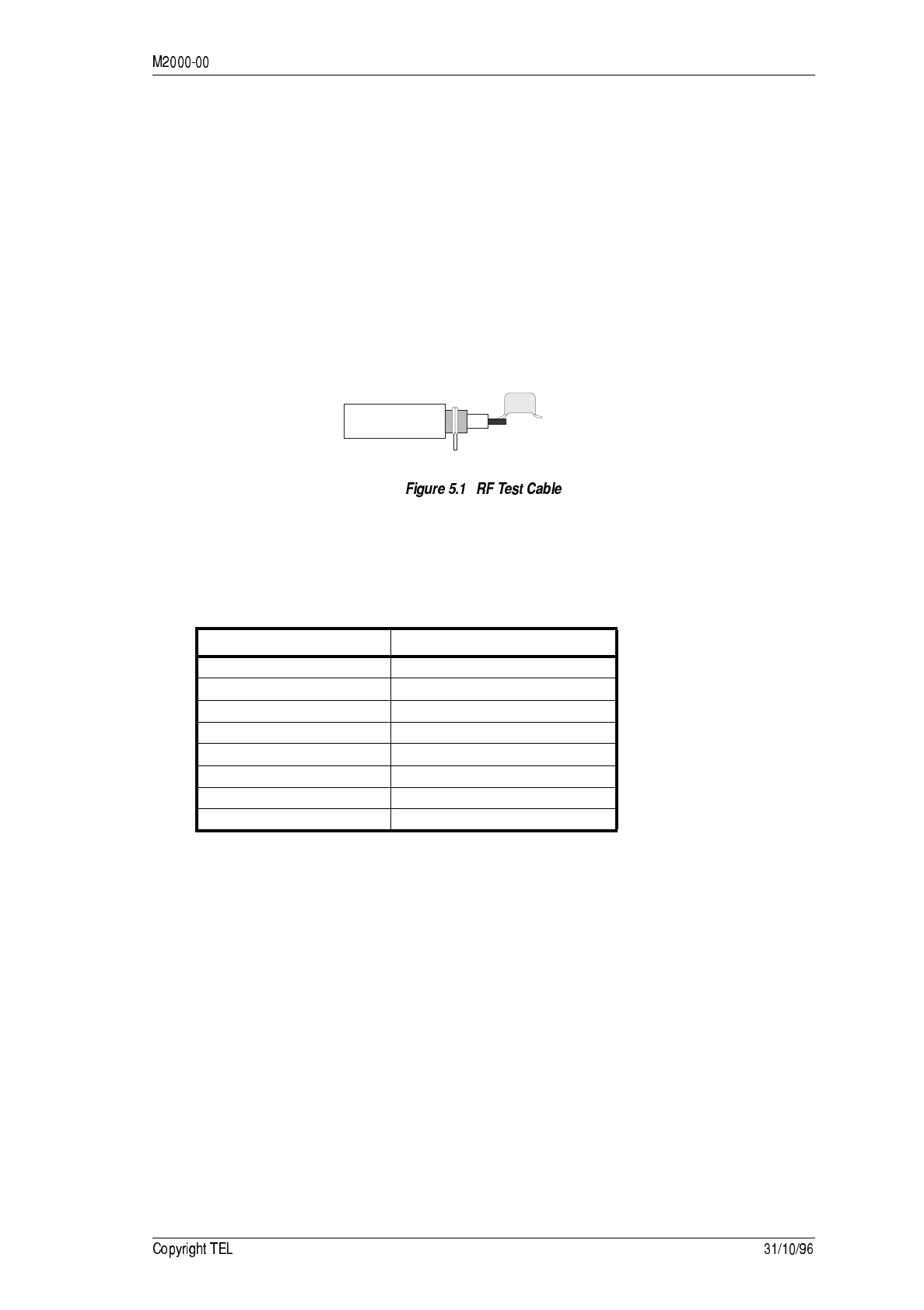
+8+
+8+8 3
Refer to the “Synthesiser Faults”, “Receiver Front End Faults” and “Receiver IF
Faults” fault finding charts in Section 5.10.
Check that the VCO is on the correct frequency, and that the receiver is correctly
aligned.
Check that the sensitivity into the front end is -119dBm (typical).
If the sensitivity is low (less than -117dBm), the fault can be traced by measuring
the sensitivity into successive circuit blocks. Prepare a test cable by connecting a
1nF capacitor to the end of a length of coaxial cable, as shown below.
Before using the test cable, ensure the coax braid is connected to an earth point
on the PCB.
Using the RF test cable, apply a modulated signal to test points in the first IF sec-
tion, at the first IF frequency, as follows:
Alternatively, apply an on-channel RF signal to the front end test points.
Poor sensitivity indicates a fault in one of the circuit blocks following the test
point. For typical sensitivity levels, refer to the fault finding charts.
Poor sensitivity at the mixer input can be caused by lack of drive level from the
VCO.
+8- 3)#9
Measure in-circuit RF levels with an RF probe. Typical RF levels can be found in
the “Transmitter RF Low Power Faults” fault finding chart, in Section 5.10.8.
Shorten the RF probe earth lead to a minimum.
Model First IF Frequency (MHz)
T2000-100 27.7
T2000-200 10.7
T2000-300 27.7
T2000-400 27.7
2000-500 49.1
T2000-600 49.1
T2000-700/900 49.1
T2000-800 61.9
1nF
Coax
To Test Cable
Connect To Earth

+8-
+8. 9)#9
+8.8 6)#9
This checks that the local base station repeater is on air and checks that the correct base
station frequency is programmed into the radio.
+8.88 1 1
Reprogram the first normal hunt channel to be the base station repeater channel
number.
Enter test mode (refer to Section 5.8, “Trunked Radios: Test Mode”).
Press the front panel key, and the FFSK should be audible.
+8.88 1"1
Enter test mode (refer to Section 5.8, “Trunked Radios: Test Mode”).
Enter the base station repeater channel number, and the FFSK should be audible.
+8.8 6))=
This checks that the radio is hunting the base station control channel. Refer to the
“Trunked Radios: Radio Won’t Acquire A Control Channel” fault finding chart in Sec-
tion 5.10.11.
Do not enter test mode.
Monitor pin 15 of IC510 (modem IC) on the T2030 or T2040 logic PCB, with a
scope probe.
FFSK should be visible for 100ms as the radio scans (hunts) through the channels.
If the radio does not lock onto the required channel, this indicates one of the fol-
lowing faults:
• The parameters on the network identity page are incorrect.
• The acquisition authorisation is incorrect.
• The signal is not opening the mute (receiver mute fault, refer to the “Receiver
Mute Faults” fault finding chart in Section 5.10.6).
• The programmed logical channel number is incorrect (even if the frequencies
are correct).
C4

+8.
+8/ 9
+8/8 *7
The test mode facility enables the trunked radio to emulate a multichannel radio, utilis-
ing the frequencies reserved for trunking. The radio can then be tested and aligned, as
described in Section 4 and Section 6.
There are two test modes provided: manual and computer controlled.
•Manual Test Mode (MTM): Commands are entered and test results are displayed
using the keys, LEDs and the display on the control head.
•Computer Controlled Test Mode (CCTM): Test commands are accepted via the
serial port of the radio, and test results are returned as required. Although this mode
is primarily intended for automated production testing, it may also be useful in the
field.
No test facilities have been provided for functions relating to non-trunked operating
mode (e.g. CTCSS), as these functions can be easily tested in non- trunked mode.
Within this Section, the following conventions apply:
• Characters within “ “ indicate a string sent or received via the serial communica-
tions port of the radio, e.g. a command code or an error code.
• Numbers without “ “ are function numbers, manually entered via the control head
in MTM to select particular test functions.
) When in test mode, connect the antenna socket to a dummy load to pre-
vent interference with trunking systems. Avoid testing on channels in use
locally.
+8/8 >?
Switch the radio off and remove the top cover.
Place a temporary link across the two pads labelled TEST MODE on the logic
PCB.
Switch on the radio:
•T2030 radios: all the front panel indicators will illuminate briefly.
•T2035 and T2060 radios: the display will show “- -” for a short time.
•T2040 radios: the control head will display “TEST MODE” for a short time.
Remove the link. The radio will remain in test mode until it is next switched off.
+8/
In MTM, the following operations are common to T203X, T2040 and T2060 radios:
• A short beep is sounded after every key press.
• All models accept the reset command character (^).
• The microphone PTT switch functions as in normal operation, i.e. a PTT press/
release selects transmit and receive respectively.
• LEDs or LCD annunciators are used to indicate transmit, synthesiser lock status and
receive signal detect status (refer to Table 5.2, “Radio Mode/Status Display”).
MTM can also be selected by sending the MTM select command while in
CCTM or program mode (refer to Table 5.1, “T2000 Test Facilities”), then
switching the radio off then on again.
This mode selection is ‘sticky’, in that the radio will always power- up in MTM
if no serial device logs on, regardless of the state of the test link. This automatic
mode selection can only be cleared by sending the appropriate command (refer
to Table 5.1, “T2000 Test Facilities”).
Increment channels in MTM by shorting S14 pin 10 (/EMRGNCY) to ground.
When the highest channel is reached, the next increment selects the lowest
channel.
+8/88 1 141 +*&
1 1
Four preset channels are available via the four preset keys to , and their
associated LEDs show the current channel. All four channels can be programmed to any
frequency within the full coverage band of the radio.
• selects the channel with the lowest number (i.e. the lowest channel in the net-
work).
• selects halfway between the highest and lowest channels available, rounding
up to the nearest channel.
• selects the channel with the highest number (i.e. the highest channel in the
network).
• selects the first channel in the normal hunt list.
1 +
• To select a channel, enter the channel number required using the front panel keys,
and press the key .
• The key enables & disables the minimum shift keying (MSK) modem
transmit, and the LED momentarily shows status. Action of the key is push-on/
push-off. When the modem transmit is enabled, the microphone audio is muted and
when the modem transmit is disabled, the microphone audio is unmuted.
When the radio is in receive, the modem transmit is temporarily disabled (and the
microphone audio is muted), but this is not shown by the LED.
C1 C4
C1
C2
C3
C4
+80
• The key selects MSK modem transmit test patterns. The LED
is off for zeros, on for ones and flashing when preamble is being sent. Successive
depressions of the key will scroll through the three states. Whenever the
key is pressed, the modem transmit is enabled unless the radio is in receive, in
which case the LED will illuminate momentarily.
• The key controls the transmit power output of the radio. The LED
is off for low power, on for high power and flashes when maximum power has been
selected. Successive depressions of the key will scroll through the three states.
Each time the channel is changed, the transmit power is reset to the level pro-
grammed for the new channel and is indicated by the LED.
+8/88 1"141+1*&
Test functions are selected by entering a two digit number followed by the
key .
Channels are selected by pressing the key (“Chan” will appear in the display),
followed by a one to four digit channel number and terminated with the
key.
After every valid command execution, a confirmation will appear in the control head
display in the form of a message. A confirmation tone is also sounded. Entries that are
invalid for any reason, e.g. an invalid function or channel number, result in a displayed
message and a warning tone.
+8/8 )&)>))?
In CCTM, test commands are accepted via the serial port of the radio and test results are
returned as required. To send and receive commands from the radio it is necessary to
run a ‘dumb terminal’ emulation program on a PC.
The serial communications port parameters are as follows:
• Logic levels:
Out: 0V = ‘1’, +5V = ‘0’
In: -12V to 0V = ‘1’, +3V to +12V = ‘0’
• A programming lead may be used to convert the output to RS232 voltage levels.
• No handshaking (RTS, CTS etc. not implemented).
•Full duplex.
• 4,800 baud.
• One start bit, eight data bits, one stop bit, no parity.
• Flow control: Xon/Xoff

+81
+8/8 8 ))#
After power-up, a reset command or a hardware reset, the radio sends the logon prompt
character “v”. Replying with an ASCII “%” within 500ms of the prompt will put the
radio in CCTM.
The radio will confirm engagement of CCTM by sending the prompt “-”, preceded by a
“CR”.
If no reply is received within the required period, the radio will engage normal
trunked mode, or MTM if the test link is fitted or the ‘sticky’ MTM is active.
If CCTM is engaged when the test link is fitted, the radio sends an error message and
gives a unique error indication (refer to Table 5.2, “Radio Mode/Status Display”).
While in CCTM, MTM can be selected (refer to Section 5.8.2). This will not come into
effect until after the next power-up or reset. To re-engage CCTM without switching the
radio off then on, a reset command can be sent to reset the radio and restart logon
prompting.
+8/8 8 ))#
• The radio accepts commands in any of the following formats:
-A two digit ASCII string selects the corresponding test function.
-A “*” character followed by a one to four digit channel number (in ASCII) sets the
radio to that channel.
• Each command must be terminated with an ASCII “CR” character to initiate execu-
tion of the command.
-If the command requires no reply, the radio then responds with a “-” prompt char-
acter.
-If a reply is required, the radio responds with a data string followed by a “CR”
and a “-” prompt . The “-” prompt indicates that the radio is ready to accept the
next command.
• There is only ever a single reply string to any command.
• Invalid commands, e.g. an invalid function number or channel number or invalid
characters in a command, cause a “{C01}”, followed by “CR” and “-”, to be sent in
reply, indicating a command error.
• In CCTM the radio will accept a reset command character (refer to Section 5.8.5).
• ASCII line feed characters are permitted at any time, but are ignored so that test
commands may be terminated with “CR” or “LF”.
• All switches (including PTT, hook etc), keys and displays on the front panel or con-
trol head of the radio are disabled while in CCTM, and no tones are sounded.

+8
+8/8" 7%&
When manual or automated test mode is engaged after logon, the radio will be in the
following state, where applicable to particular radio models. The numbers in brackets
refers to the test facility, as described in Table 5.1, “T2000 Test Facilities”.
• Synthesiser programmed to the last selected channel.
• Modem transmit off (13).
• Force receive audio muted if in transmit mode (20).
• Force receive audio unmuted if in receive mode (21).
• Microphone audio muted if in receive mode (22).
• Microphone audio unmuted if in transmit mode (23).
• Radio power amplifier enabled (31).
• Radio set to receive if PTT released on power-up (32).
• Radio set to transmit if PTT pressed at power-up (33).
• 13.8V switched supply on / ECN off (43).
• Radio not in state for current measurement test (45).
• Microprocessor clock rate set as programmed for the channel if in receive mode.
• Microprocessor clock rate ‘normal’ if in transmit mode (70).
• Radio transmit power set as programmed for the channel.
The behaviour of the front panel or control head digital display and/or LEDs is
described in Table 5.2, “Radio Mode/Status Display”.
+8/8+ 3#!
+8/8+8
The radio may be reset at any time in any of the following ways:
• Switch the radio off then on again.
• Momentarily connect the microprocessor ‘reset’ pin to ground (pads are provided on
the enhanced control PCB).
• Send a reset command character (^) over the serial communications port (refer to
Table 5.1).
The radio will not respond to the reset character after an EPROM or RAM test
failure.
+8
+8/8+8 3#
The following table lists the test facilities available in MTM and CCTM for the T203X,
T2040 and T2050. Facilities for the T2010, T2015 and T2020 are also listed for compari-
son, and further information about the tests is listed following the table.
Within the table, a ‘-’ indicates the corresponding facility is not available, and “nnnn” is
a one to four digit channel number (leading zeros are permitted).
T2010/T2015 T2020 T203X T2040/T2050
Normal CCTM Normal CCTM Man Auto Man Auto
Signalling functions:
10. set modem to send zeros
11. set modem to send ones
12. set modem to send preamble
13. disable modem Tx
14. read modem Rx state
15. disable subaudible signal
16. enable subaudible signal
17. read signalling decode status
-
-
-
-
-by
channel
speaker
-
-
-
-
-
-
-
“17”
-
-
-
-
-by
channel
speaker
-
-
-
-
-
“15”
“16”
“17”
&
keys
-
-
-
-
10
11
12
13
14
-
-
-
10
11
12
13
-
-
-
-
“10”
“11”
“12”
“13”
“14”
-
-
-
Mute functions:
20. force Rx audio muted
21. force Rx audio unmuted
22. mute microphone audio
23. unmute microphone audio
24. let squelch control Rx audio
25. read squelch Rx busy status
26. relax Rx audio mute control
-
l-MON*
-
-
s-MON
-
s-MON
-
“21”
“22”
“23”
“24”
-
“26”
-
l-MON
-
-
s-MON
-
s-MON
“20”
“21”
“22”
“23”
“24”
“25”
“26”
-
-
-
-
-
“20”
“21”
“22”
“23”
“24”
“25”
-
20
21
22
23
24
-
-
“20”
“21”
“22”
“23”
“24”
“25”
-
Radio Rx/Tx functions:
30. inhibit the PA (Tx mode)
31. enable the PA (Tx mode)
32. set radio to Rx
33. set radio to Tx
34. set PA to low power
35. set PA to high power
36. set PA to max power
37. relax PA power control
-
-
see
below
by
channel
-
-
-
“32”
“33”
“34”
“35”
“36”
“37”
-
-
see
below
by
channel
-
-
-
“32”
“33”
“34”
“35”
“36”
“37”
-
-
-
-
useor
key
-
“30”
“31”
“32”
“33”
“34”
“35”
“36”
-
30
31
32
33
34
35
36
-
“30”
“31”
“32”
“33”
“34”
“35”
“36”
-
Power supply functions
42. 13.8VSW off /ECN on
43. 13.8VSW on /ECN off
44. set radio state for current
measurement
45. cancel current measurement
state
-
-
-
-
-
-
-
-
-
-
-
-
“42”
“43”
-
-
-
-
-
-
“42”
“43”
“44”
“45”
42
43
-
-
“42”
“43”
“44”
“45”
RSSI functions:
61. Set L1 threshold
62. set L2 threshold
63. read averaged RSSI level
64. read L1
65 read L2
-
-
-
-
-
-
-
-
-
-
-
-
-
-
-
-
-
“63”
-
-
-
-
-
-
-
“61”
“62”
“63”
“64”
“65”
61
62
63
64
65
“61”
“62”
“63”
“64”
“65”
Miscellaneous functions:
70. select normal µP clock rate
71. select birdie µP clock rate
72. read synth. lock status
73. relax µP clock control
-
-
-
-
-
-
-
-
by
channel
-
-
“70”
“71”
“72”
“73”
-
-
-
-
“70”
“71”
“72”
-
70
71
-
-
“70”
“71”
“72”
-
Fn
Fn
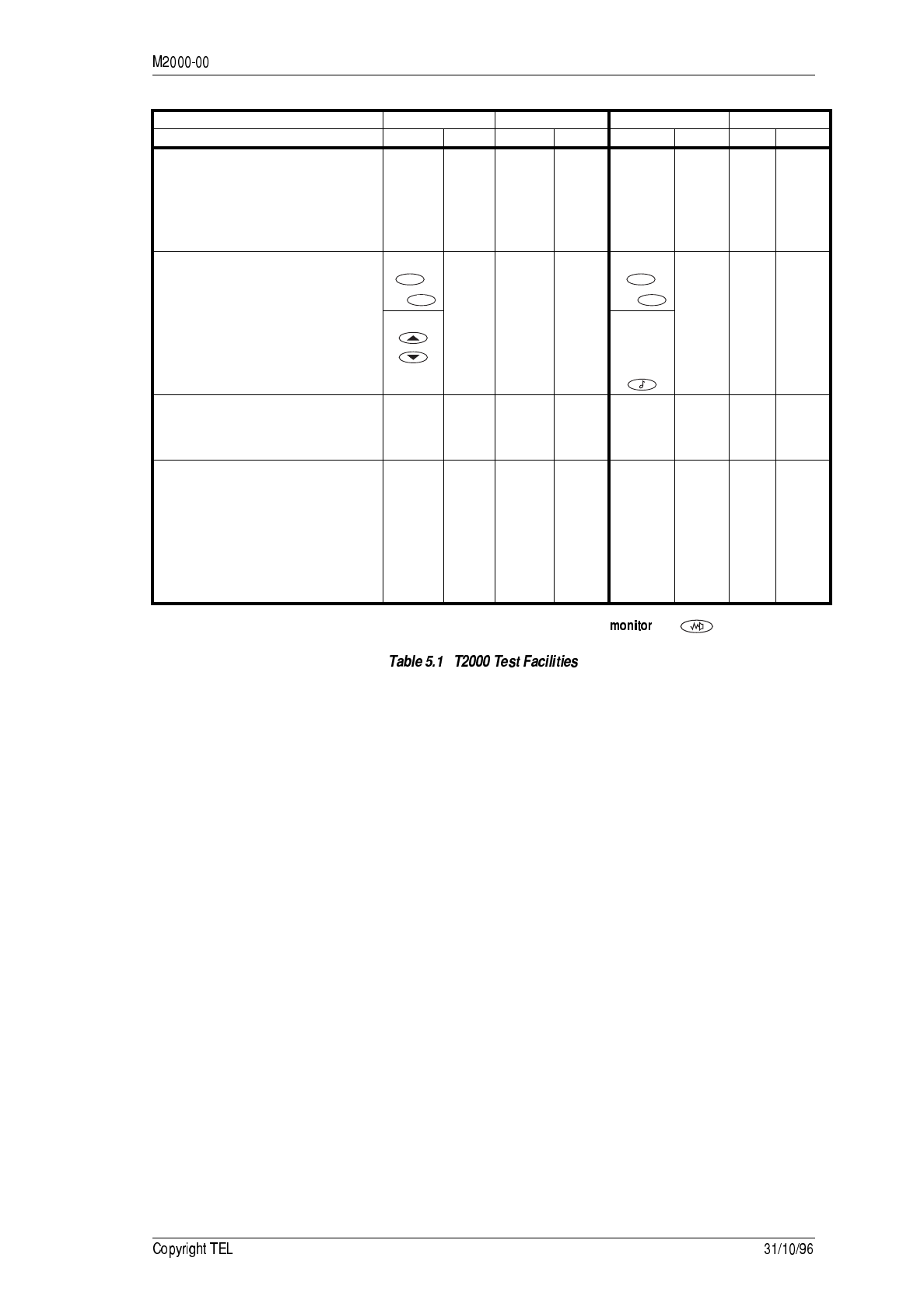
+8
• In MTM, functions 10 - 13, 21, channel selection and PTT control of receive/transmit
are all required for MPT1352 testing. Type approval testing requires the channel
increment facility using an external input.
• All test function requests are valid when the radio is in either receive or transmit but
some functions (10, 11, 12, 21, 23 and 24) take effect only when the radio is in the
appropriate mode.
•10 - 13, 22, 23: When any of the functions which set the modem sending test data are
selected (functions 10 - 12), the microphone audio is automatically muted. When the
microphone audio is unmuted using function 23, the modem transmit is disabled.
When the radio is in receive, the microphone audio is temporarily muted and the
modem transmit is temporarily disabled. This prevents any unwanted TCXO
modulation which may occur on radios with dual point modulation.
These automatically selected states can be overridden until the next transmit to
receive transition. If microphone unmute or modem transmit enable is requested
when the radio is in receive, these functions will not be actioned until the radio is
in transmit.
•10, 11, 12: The two modem data states selected by functions 10 and 11 are ‘0’ =
1800Hz tone and ‘1’ = 1200Hz tone respectively. Preamble, selected by function 12, is
alternating 1800 and 1200Hz tones at a rate of 1200 baud.
*‘
l-MON’ & ‘s-MON’ indicate a long (>1s) and a short (<1s) press of the key , respectively.
Special functions:
92. set ‘sticky’ MTM
93. clear ‘sticky’ MTM
94. read serial number
95. read factory model ID
99. get current channel number
-
-
-
-
-
-
-
“94”
“95”
-
-
-
-
-
-
-
-
“94”
“95”
-
-
-
-
-
-
“92”
“93”
“94”
“95”
-
-
-
-
-
-
“92”
“93”
“94”
“95”
-
Radio channel control:
select a channel T2010:
to
‘*n” chan “*nnn”
T2030:
to
“*nnn” *nnn “*nnn”
T2015:
keys
T2035:
Select
channel
& press
Single character commands:
reset the radio
select programming mode
select auto test mode
“^”
“#”
“%”
“^”
“#”
“%”
“^”
“#”
“%”
“^”
“#”
“%”
“^”
“#”
“%”
“^”
“#”
“%”
“^”
“#”
“%”
“^”
“#”
“%”
Radio controls & indicators:
PTT press = select Tx mode
PTT release = select Rx mode
channel increment input
Tx indicator
synth. out of lock indicator
RF signal detected indicator
yes
yes
-
Tx
flash
chan
LED
BUSY
-
-
-
Tx
flash
chan
LED
BUSY
yes
yes
-
Tx
flash
TX &
BUSY
BUSY
-
-
-
-
-
-
yes
yes
pin 10, S14
TX
SVC
GO
-
-
-
-
-
-
yes
yes
ECR
TX
SVC
GO
-
-
-
-
-
-
T2010/T2015 T2020 T203X T2040/T2050
Normal CCTM Normal CCTM Man Auto Man Auto
1
1
4
C1
C4
+8"
•14, 25, 72: These functions return a Boolean radio status value, either a ‘0’ or a ‘1’, as
follows:
•20: The receive audio is muted temporarily to quieten the speaker whenever the
radio is in transmit. This state may be temporarily overridden until the next receive
to transmit transition. If ‘force Rx audio unmuted’ (21) or ‘let squelch control Rx
audio’ (24) is requested when the radio is in transmit, the function will not be
selected until after the radio is in receive.
•32, 33: Functions 32 and 33 are provided in MTM so that the radio transmit state can
be sustained without the need to hold the PTT depressed. Caution must be exercised
to prevent the power amplifier from overheating.
•42, 43: Select economy/non-economy state. In economy state the audio power
amplifier is disabled and the front panel backlighting is set to its programmed econ-
omy state. In non-economy state, the audio power amplifier is enabled and the back-
lighting is set to its normal programmed state.
•44, 45: Engage/disengage radio state for measurement of typical trunked mode sup-
ply current drain. In this state only the ‘SVC’ and ‘C1’ LEDs are switched on and
non-economy state is selected (function 43). Upon disengagement, the previous dis-
play is reinstated but the economiser state is not altered.
•61, 62: To set up the RSSI thresholds, apply an RF signal to the radio (on an appropri-
ate receive channel) at the threshold level. Allow at least 400ms for the RSSI averag-
ing to settle, then select function 61 or 62 as required.
The averaged RSSI threshold value (in decimal full scale = 255) is either displayed if
in MTM or returned via the serial port if the radio is under computer control. The
value is also stored in the radio’s database (in the microprocessor EEPROM) and the
database checksum is automatically updated.
•63: In MTM, function 63 gives a regularly updated display of the averaged RSSI
value. The leftmost decimal point will light when the RSSI level equals or exceeds
L1, and the rightmost decimal point will light when the RSSI level equals or exceeds
L2.
In CCTM a single averaged RSSI value is returned.
At least 400ms should be allowed after any change in signal level for the returned
value to be accurate.
•94: Returns the serial number part of the radio’s ESN as a number of up to 6 digits
with leading zeros suppressed.
•95: Returns the factory programmed ‘factory model ID’ as a string of six decimal
digits.
•99: This function is intended to allow easy modification of the current channel
number via the number entry keys.
Return Value ‘0’ ‘1’
14 - read modem Rx state data = 0 data = 1
25 - read Rx busy state no RF signal detected RF signal detected
72 - read synth lock status out of lock in lock
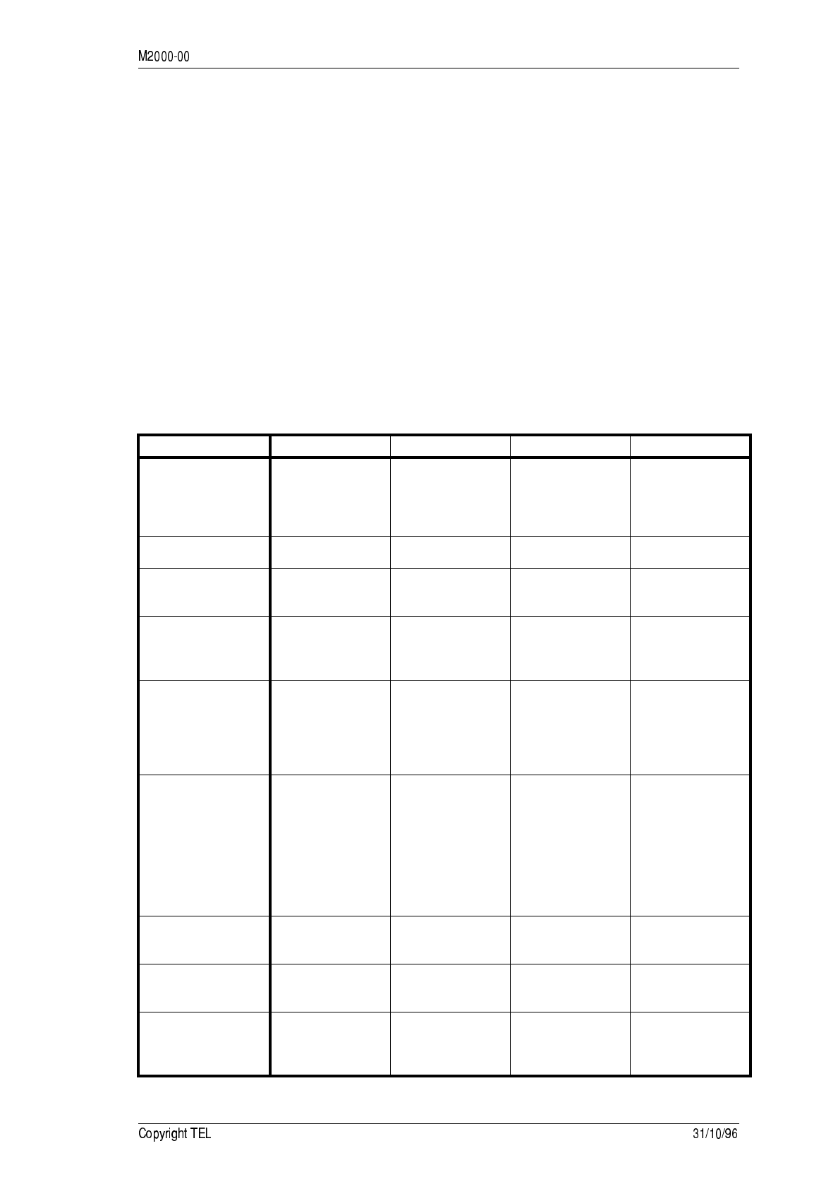
+8+
+8/8- 9&)
The mode or status of the radio is indicated by the behaviour of:
• the monitor LEDs (ML1 and ML2) on the top side of the logic PCB
• the radio control head LEDs.
Unless otherwise stated, the two monitor LEDs behave as in normal operation:
• ML2 is off
• ML1 flashes at a rate of 1Hz to indicate watchdog timer ‘kick’ activity
• In normal trunked radio mode, ML2 flashes at a rate of several Hertz. This indicates
control channel hunt or codeword reception on a control channel.
A value in brackets { } with a mode/status description indicates that the radio sends an
error message via the serial port upon engaging that mode/status.
This table identifies display states for trunked radios, with non-trunked models for
comparison.
Mode/State T2010/T2015 T2020 T2030/T2035 T2040
CONFIG error
Monitor LEDs
flashing together.
Display shows
“CONF-ERR”
Monitor LEDs
flashing together.
Top & bottom row
LEDs flashing. C1
LED on (if fitted)
Monitor LEDs
flashing together.
Display shows
“CONF-ERR”
CONFIG register
programmed Display shows
“CONF-PGM” Display undefined Display shows
“CONF-PGM”
ROM or RAM test
failure
CTCSS output tog-
gling. Display
undefined
Tone output tog-
gling. Display
undefined
Tone output tog-
gling. LEDs unde-
fined
Tone output tog-
gling. Display
undefined
ESN checksum error
{X31}
(go to program
mode)
As for program
mode + CLR LED
flashing. T2035: dis-
play shows “-U1”
Display shows
“ESN-ERR”
Database checksum
error {X32}
(go to program
mode)
As for program
mode.
2010: all channel
LEDs on
2015: display shows
“00”
Display shows
“-PROG-”
Top row LEDs on
As for program
mode + DESP LED
flashing.
T2035: display
shows “-U2”
Display shows
“-DATA-ERR-”
Top row LEDs on.
System error
{Enn}
Monitor LEDs
alternately flashing
“-ERROR nn” in
display (nn = error
mumber)
Monitor LEDs &
top row LEDs flash-
ing.
2 digit BCD error
number on bottom
rows.
T2035: display
flashes error
number
Monitor LEDs
alternately flashing.
“ERROR nn” in dis-
play (nn = error
mumber)
MOBD link left in &
CONFIG register OK
{X06}
Display error
shows
“MODB-ERR”
Top & bottom row
LEDs flashing + C2
LED on (if fitted)
Display shows
“MODB-ERR”
Logon with test link
in
{X07}
Top & bottom row
LEDs flashing + C3
LED on (if fitted)
Display shows
“TLINK-ERR”
Key/LED test failure
{X04}
LED flashing
shows error - all
LEDs to right &
below on
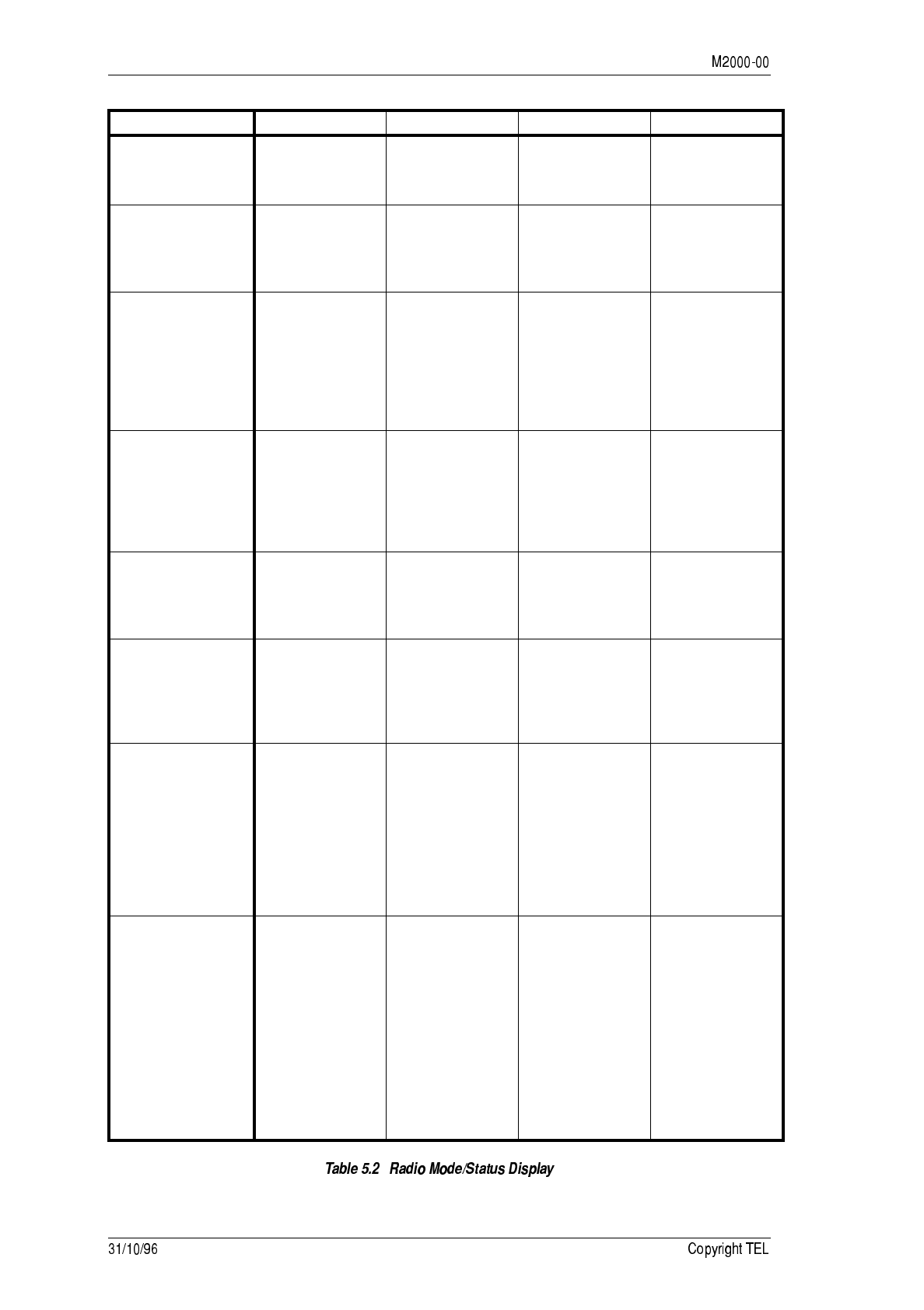
+8-
Program mode
2010: all channel
LEDs on
2015: display shows
“00”
Display shows
“-PROG-”
Top row LEDs on
Top row + C1 LEDs
all on (if fitted)
T2033/35: display
shows “-UU”
Display shows
“-PROG-”
Top row LEDs on
Cloning mode
AUX LED flashing.
AUX/SCAN LEDs
flash if clone failed.
Target radio in pro-
gramming mode.
Display shows
“CLONING” Top
row LEDs on. Tar-
get radio in pro-
gramming mode.
Manual Test Mode
(MTM)
All LEDs on for a
short time then
indicate radio sta-
tus.
C1 to C4 show last
channel (if fitted).
T2035: display
shows “- - -” briefly
Display shows
“chan xxxx” (xxxx
= last channel
number). LEDs
indicate radio sta-
tus
Key pressed at
power-up
(control head test)
[AUX] = clone
[CALL] = program Any key on the
control head & any
mode.
All LEDs & all LCD
segments are set
flashing indefi-
nitely
C1 key (if fitted) in
MTM
- a front panel key/
LED test is initi-
ated - all LEDs on
initially
Any key on the
control head & any
mode. All LEDs &
all LCD segments
are set flashing
indefinitely
Computer Control-
led Test Mode
(CCTM)
Front panel shows
normal radio state
(not a separate
mode)
Display shows
“-AUTOTEST-” Top
row LEDs on
Top row + C2 LEDs
(if fitted) all on.
T2035: display
shows "- - -" contin-
uously
Display shows
“AUTOTEST”
Top row of LEDs on
CCI mode
Normal display
“CCI BUSY” & top
row LEDs on when
processing a com-
mand or in ‘lockout
all’ mode
Normal display
“CCI BUSY” & top
row LEDs on when
processing a com-
mand or in ‘lockout
all’ mode.
Normal radio
mode
No special power-
up sequence - nor-
mal radio state
immediatly dis-
played
Programmable
power-up message
displayed for a
short time then nor-
mal radio display
(default mode)
T2030: own number
as CD on 3 rows of
LEDs, then last
number on C1 to
C4 & DESP LEDs.
Others as labelled.
T2035: Own
number briefly on
display, then last
number called.
Own number dis-
played for a short
time after power-
up then program-
mable power-up
message followed
by normal radio
display
PTT on power-up in
MTM or normal
mode
Software version #
indicated for a
short time as
“h.nn”. “h” is
shown with the
Busy and TX LEDs
as a hex number.
“n’s” are indicated
by the two lower
rows of LEDs
(2010), or by the
channel display
(2015).
Display shows
“xxxx nn.mm” for a
short time, nn =
major, mm = minor
version number
T2030: 3 rows of
LEDs display the
software version #
for a short time as
h.nn (h is a hex
number) then as
per selected mode.
T2035: software
version number
on display.
Display shows
“xxxx nn.mm” for a
short time, nn =
major mm = minor
version number,
then as per
selected mode
Mode/State T2010/T2015 T2020 T2030/T2035 T2040
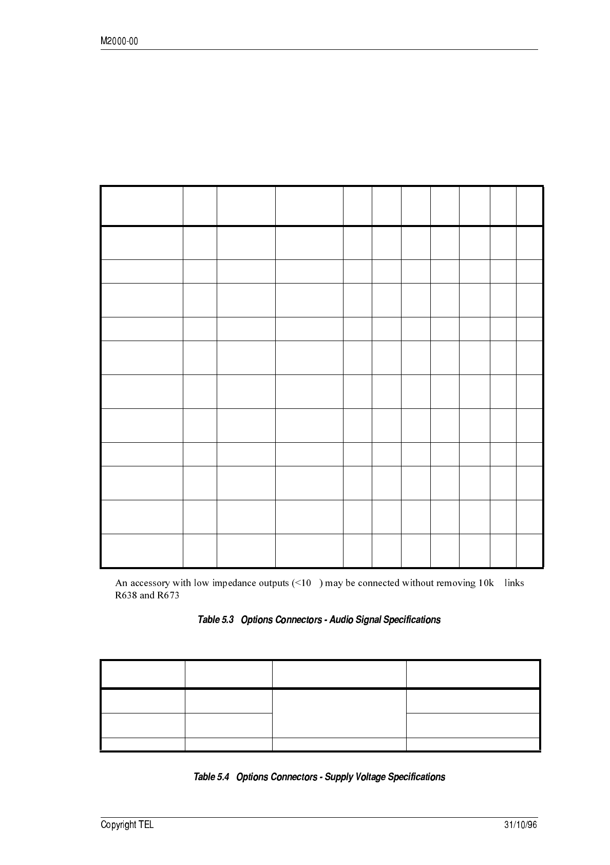
+8.
+80 *&$#&##
The options connectors, S13 and S14, are located on the top side of the T2000 logic PCBs,
and are provided for use with plug-on accessory PCBs.
The following tables describe the signals available on these connectors, and also on S15
(T2010 & T2015 logic PCB).
*Ω Ω
Connection
(to/from) Pin
No. Used
for Level for 1kHz
AF 60% FM Z1
ΩZ0
ΩMin.
ZLDC
Level Slope
dB/8
LF
-3dB
Hz
HF
-3dB
Hz
DET-AF-OUT
(from detector via
3kHz LPF)
S13-1 CTCSS
data, DCS,
Selcall
400mVp-p <1k 1k 3.3V flat 10 3.4k
ALC-IN
(to compressor) S13-2 0.2Vp-p 2.2k 0V +6 0.25k 3.4k
RX-LINE-OUT
(de-emphasised
receiver audio)
S13-3 to accessory
line interface 0.4Vp-p 100 10k 3.3V -6 0.23k
or
0.35k
3.4k
TX-LINE-OUT
(from ALC) S13-4 to accessory 1.2Vp-p <1k 1k 3.3V flat 70 33k
RX-LINE-IN
(to squelch
element)
S13-5 from
accessory 0.4Vp-p 5k*3.3V flat 0.18k 20k
TX-LINE-IN
(to pre-emphasis) S13-6 from
accessory
line interface
1.2Vp-p 5k*3.3V +6V 0.25k 3k
RX-GTD-AF
(Rx Audio from
after squelch)
S13-7 line interface 0.4Vp-p 10k 0.2M 3.3V flat 0.23k
or
0.35k
3.4k
TX-SIG-IN
(to limiter) S13-8 data Selcall 2.5Vp-p 470k 3.3V flat 4 3.4k
RX-BEEP
(to AF PA with min.
volume stop)
S13-9 sidetone 0.5Vp-p 470k AC flat 0.18k 20k
TX-LF-SIG
(to LPF) S13-10 CTCSS, DCS 5.0Vp-p for
12%
deviation
2.2k 3.3V flat 4 3.4k
OPTIONS-GND
(connected to
ground on RF PCB)
S13-11
Connection
(to/from) Pin No. Function Available Current
+13.8V-UNSW S13-12 - emergency: to bypass the on/
off switch 0.5A
+13.8V S14-1 - supply to options with own
regulators 200mA (remote loom resist-
ance = 0.43Ω/loop meter)
+5V S14-2 supply to options 150mA
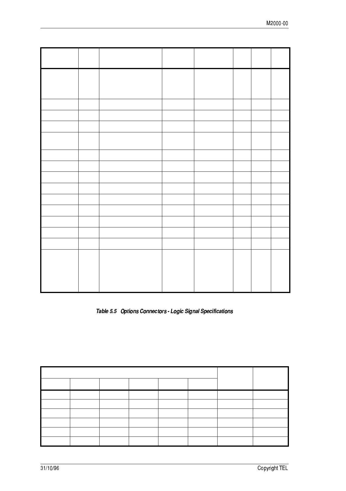
+8/
The following table shows the BCD codes for T2010 and T2015 radios under external
channel control.
T2010 has 4 channels accessible by BCD and T2015 has 24 channels accessible by
BCD
* Refer to BCD selection table.
Connection Pin
No. Function Logic
Levels Logic
Sense Sink
Imax
Source
Imax Zin
BUSY S14-3 carrier detect
opening time: <35ms
closing time: <20ms
(8dB sinad, 6dB margin)
0V 5V 0V = busy 0.5mA 0.1mA
RX-GATE S14-4 Rx audio gate information 5V CMOS 5V = audio 1.5mA 0.3mA
/PTT-TO-OPT S14-5 from mic.; linked to 18 pull-up 0V = Tx 1.5mA 50µA 2k7
/PTT-FRM-OPT S14-6 Tx 5V CMOS 0V = Tx CMOS
/IN-LOCK S14-7 synthesiser lock detect
(lock-up time: <20ms) 0V 5V 0V = lock 0.2mA 0.2mA
MIC-MUTE S14-8 disables AF from mic. only 5V CMOS 5V = mute 200k
/SIG-SQLCH S14-9 Rx audio gate control open c. 0V = AF muted 47k
/EMERGNCY S14-10 starts s/w sequence open c. 0V = emergency 10k
CALL-SW S14-11 front panel control 5V CMOS 1.5mA 0.3mA
HUSH S14-12 car radio mute output 5V CMOS 1.5mA 0.3mA
AUX-ON/OFF S14-13 front panel control 5V CMOS 1.5mA 0.3mA
HORN S14-14 Selcall horn alert 5V CMOS 1.5mA 0.3mA
RSSI S14-15 Rx signal strength 0 - 50µA 0.8µA/dB
EXTERNAL S14-16 line to power plug
BCD0
BCD1
BCD2
BCD3
BCD4
BCD5
S15-9
S15-10
S15-11
S15-12
S15-13
S15-13
channel change option
on T201X*0 - 5V CMOS 0V = 0
5V = 1 10k
BCD Channel Number Codes BCD
Number Channel
Number
BCD-5 BCD-4 BCD-3 BCD-2 BCD-1 BCD-0
000000 0 1
000001 1 2
000010 2 3
000011 3 4
000100 4 5
000101 5 6
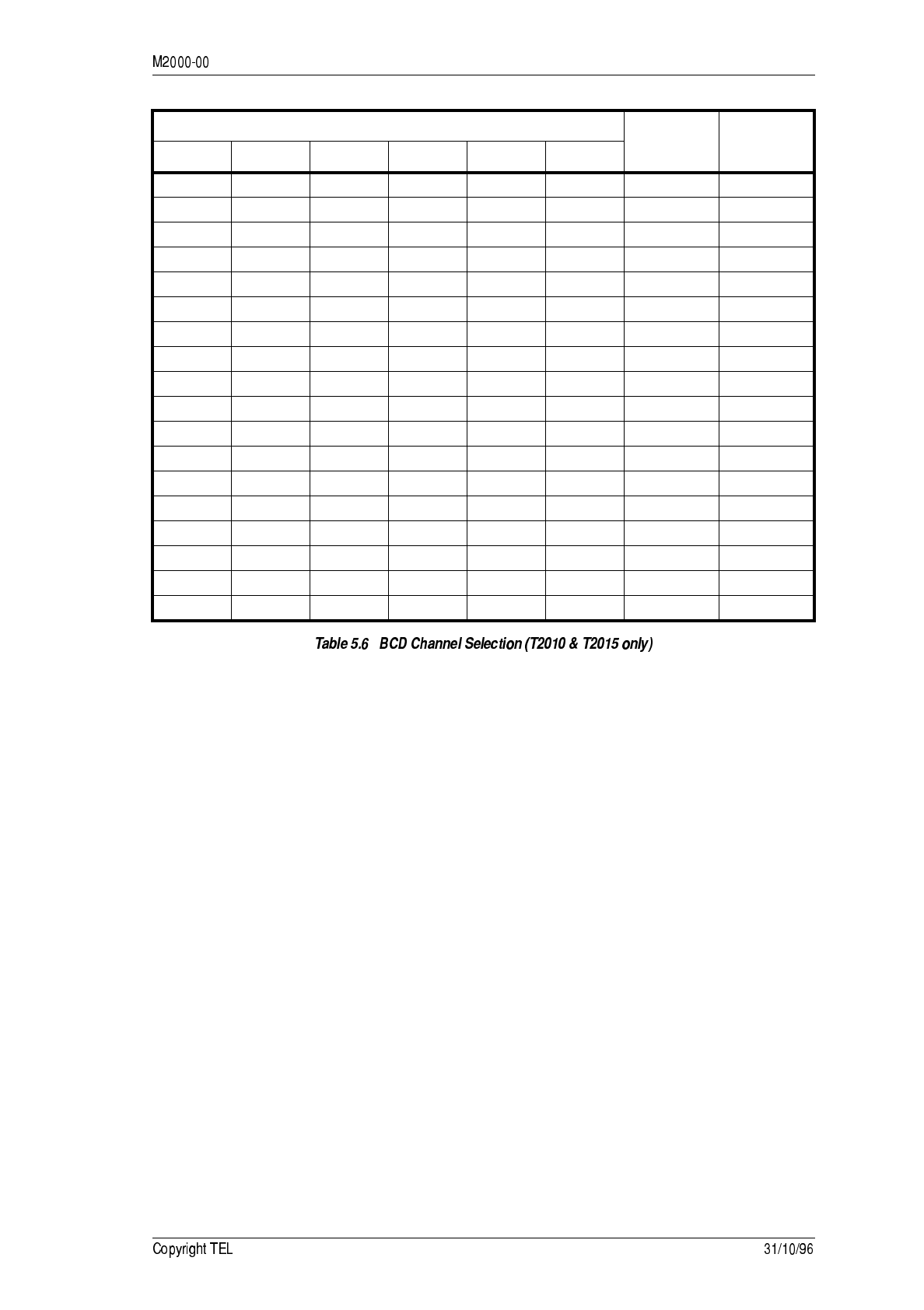
+80
)#-:./
Additional microprocessor control signals are available on the T2020, T203X, T2040,
T2050 and T2060 HC11 logic PCB (PCB IPN 220-01344-0X), on connectors S16, S17 and
S18.
000110 6 7
000111 7 8
001000 8 9
001001 9 10
010000 10 11
010001 11 12
010010 12 13
010011 13 14
010100 14 15
010101 15 16
010110 16 17
010111 17 18
011000 18 19
011001 19 20
100000 20 21
100001 21 22
100010 22 23
100011 23 24
BCD Channel Number Codes BCD
Number Channel
Number
BCD-5 BCD-4 BCD-3 BCD-2 BCD-1 BCD-0
+81
+81 33)
The fault finding charts listed below are intended to be used in conjunction with the cir-
cuit diagrams and other PCB information found in Section 7, and with the circuit
descriptions and block diagrams found in Section 2.
Section Title Page
5.10.1 Radio Won’t Switch On 5.21
5.10.2 Radio Won’t Program 5.22
5.10.3 Synthesiser Faults 5.23
5.10.4 Receiver Front End Faults 5.24
5.10.5 Receiver IF Faults 5.25
5.10.6 Receiver Mute Faults 5.26
5.10.7 No Audio On Receive 5.27
5.10.8 Transmitter RF Low Power Faults 5.28
5.10.9 Transmitter Power Control Faults 5.30
5.10.10 Transmit Audio Absent 5.31
5.10.11 Trunked Radios: Radio Won’t Acquire A Control Channel 5.32
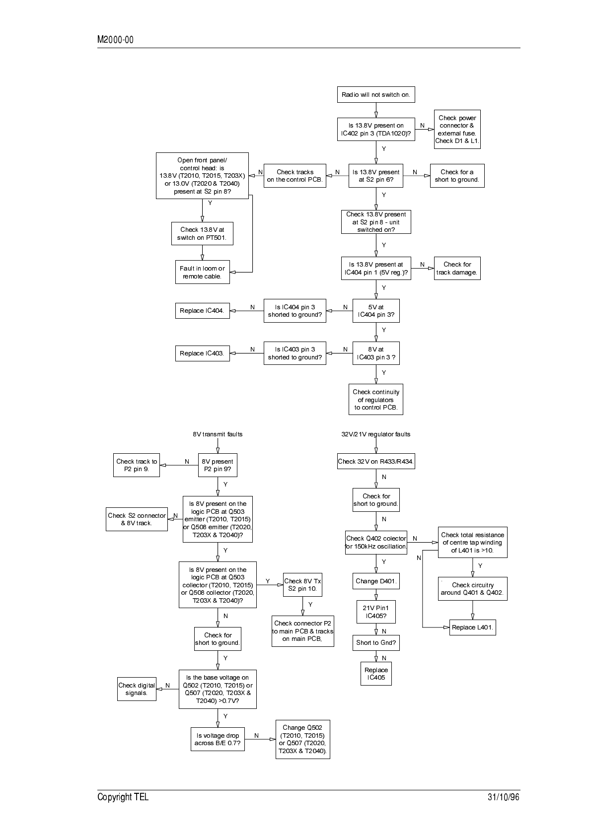
+8
+818 BD7#*
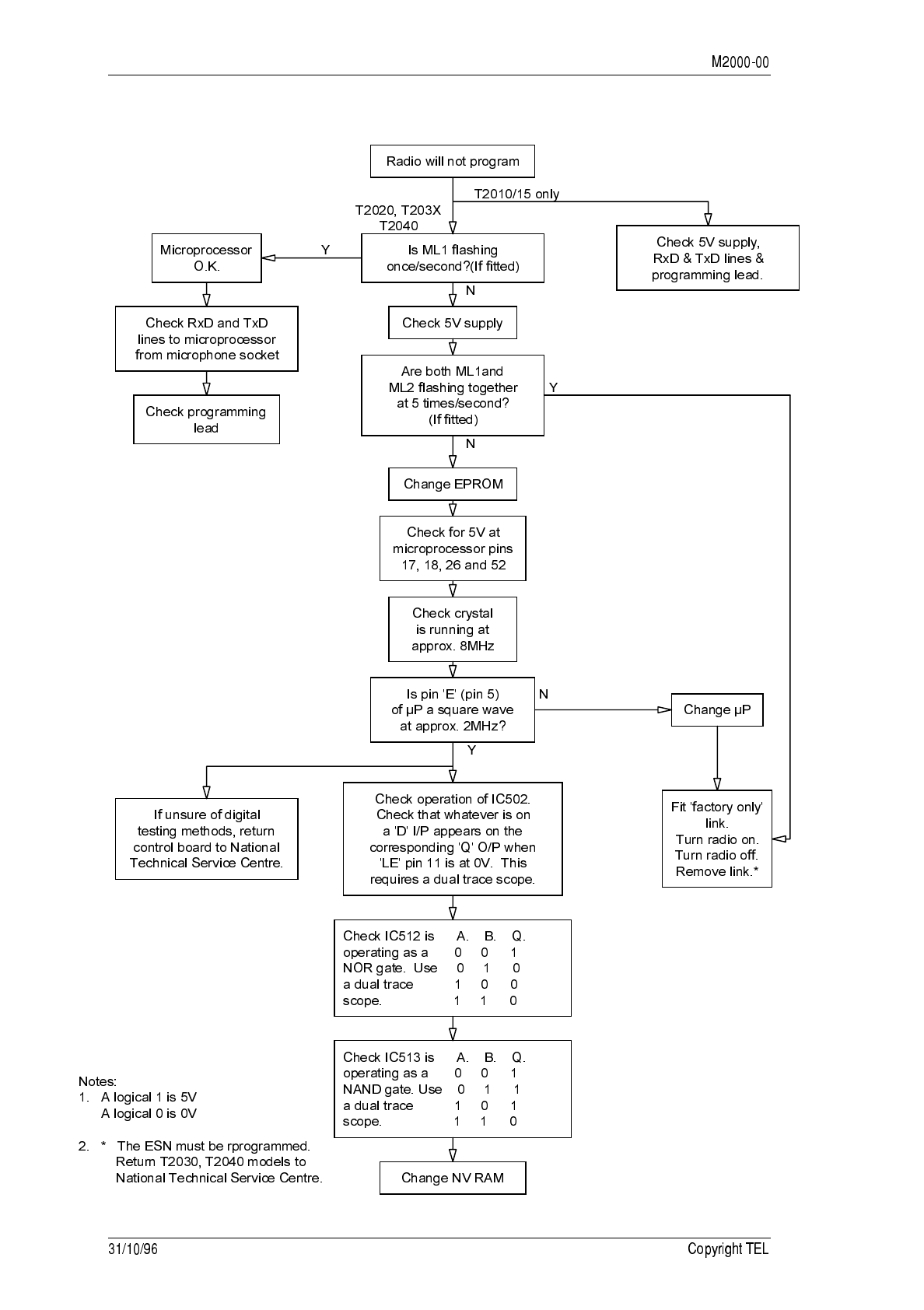
+8
+818 BD
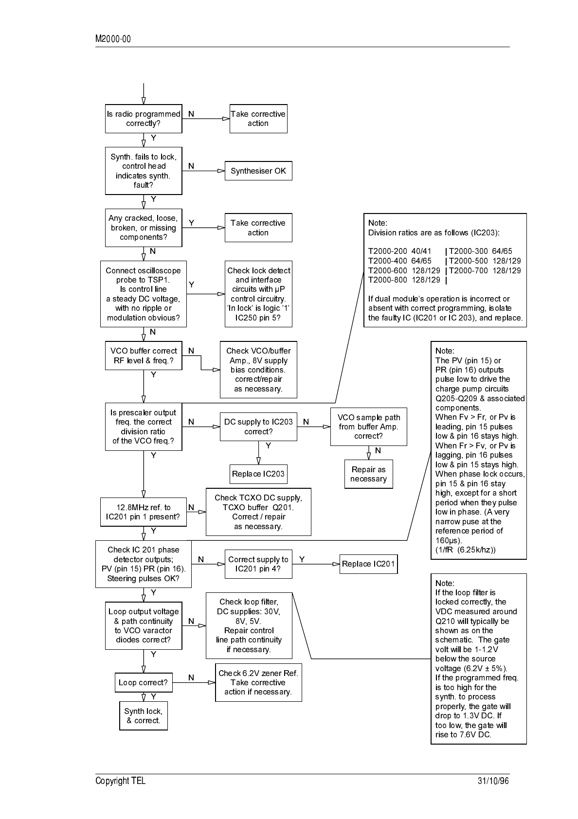
+8
+818 3
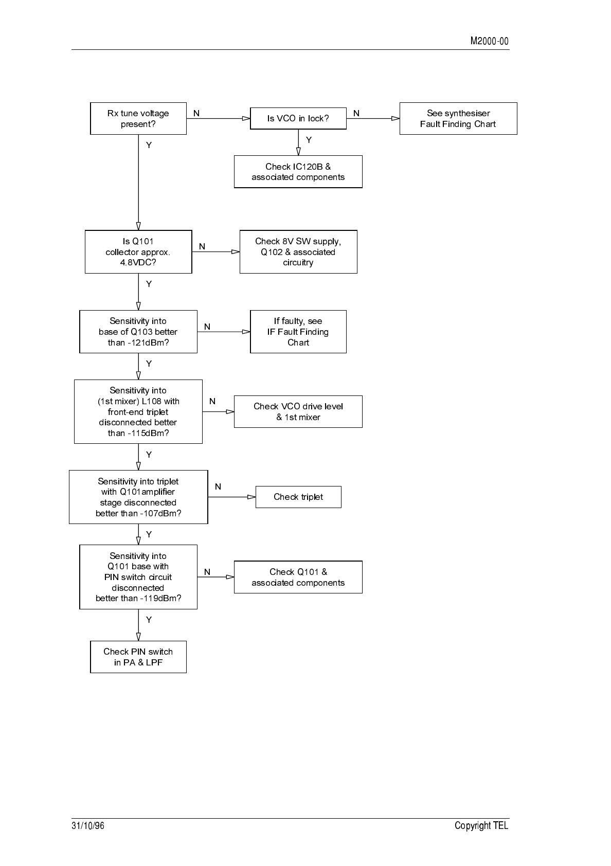
+8"
+818" #3'3
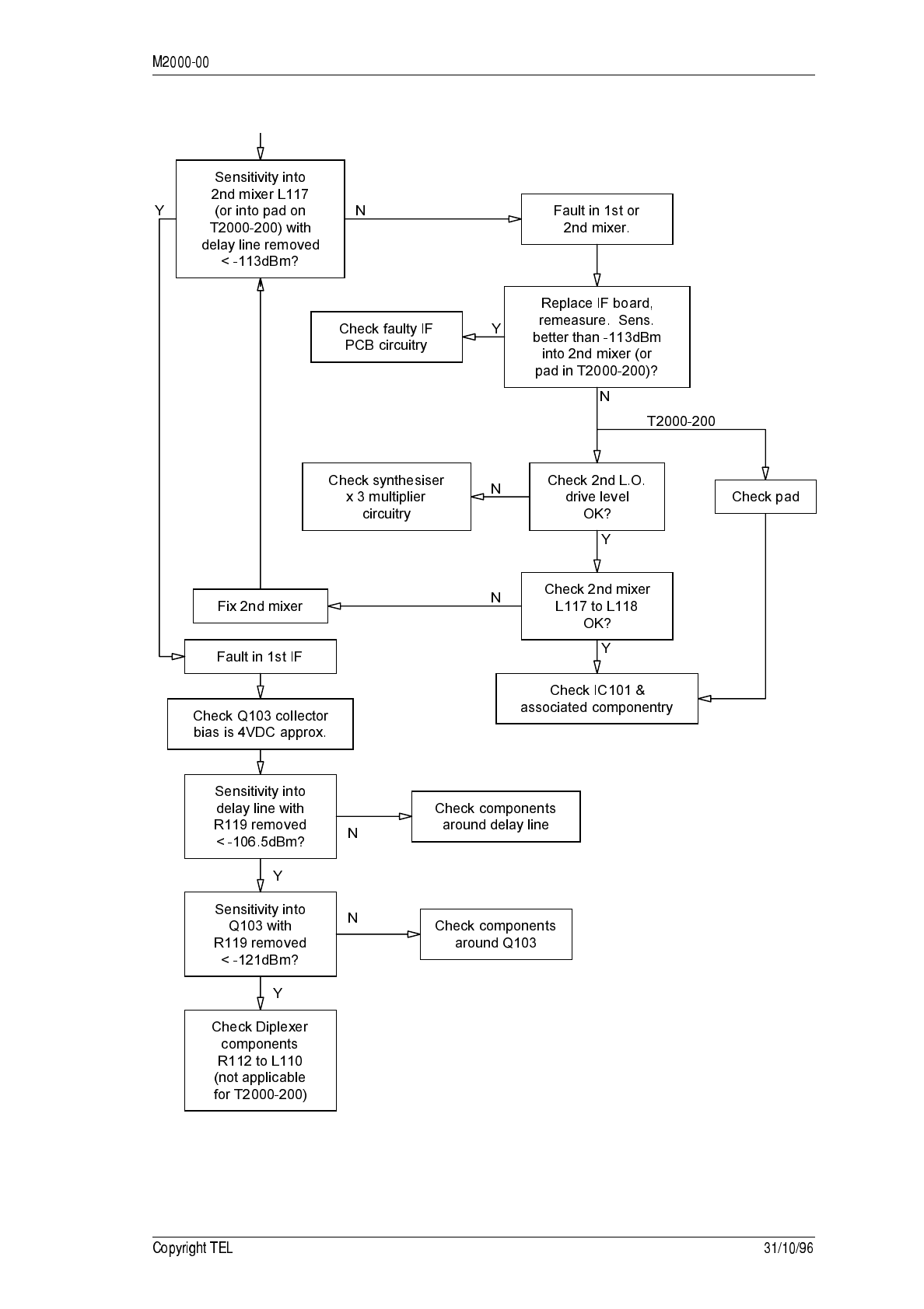
+8+
+818+ #$33
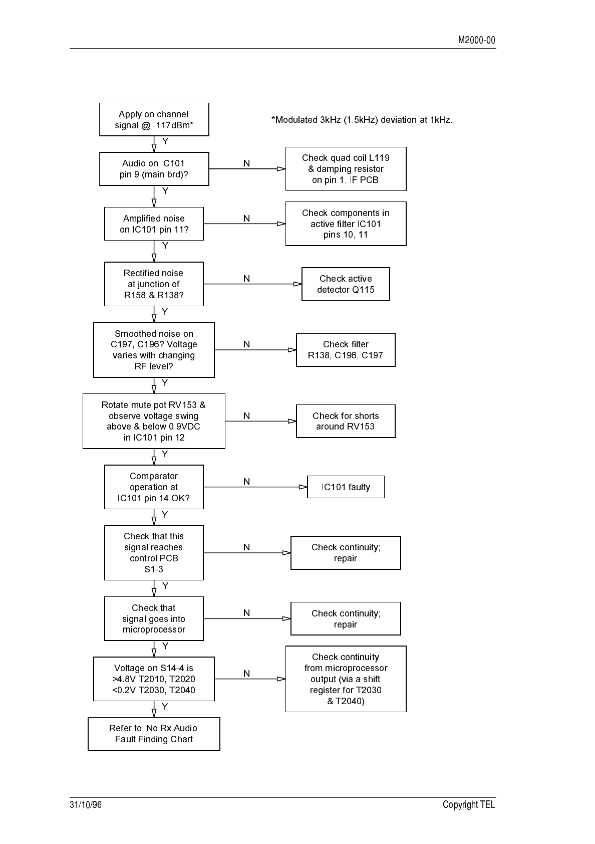
+8-
+818- #3
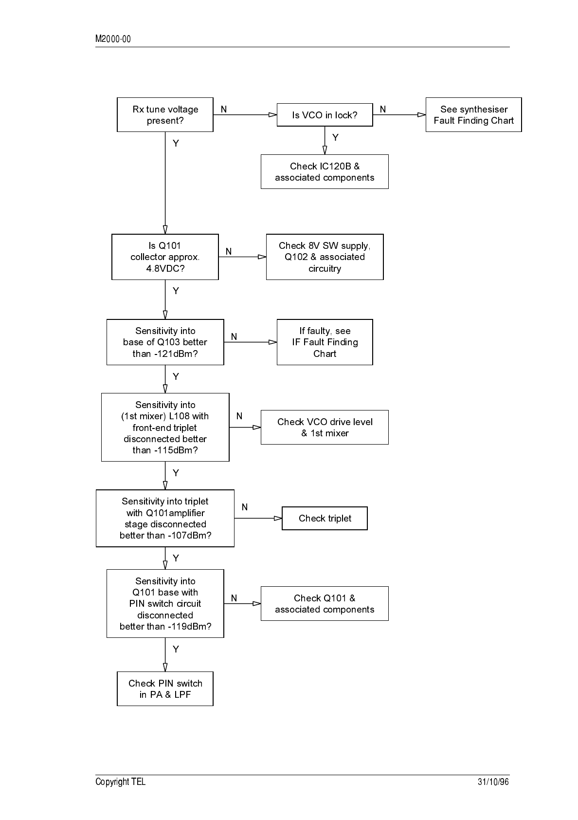
+8.
+818. A!*#
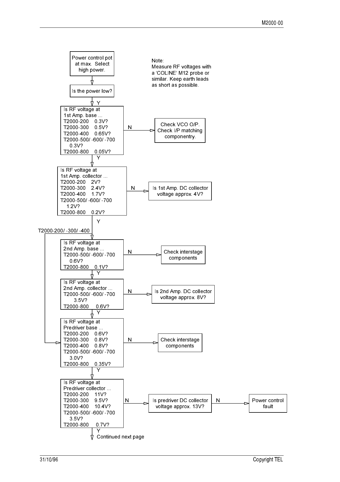
+8/
+818/ 3,773
≥
≥
≥
≥
≥
≥
≥
≥
≥
≥
≥
≥≥
≥
≥
≥
≥≥
≥
≥
≥
≥≥
≥
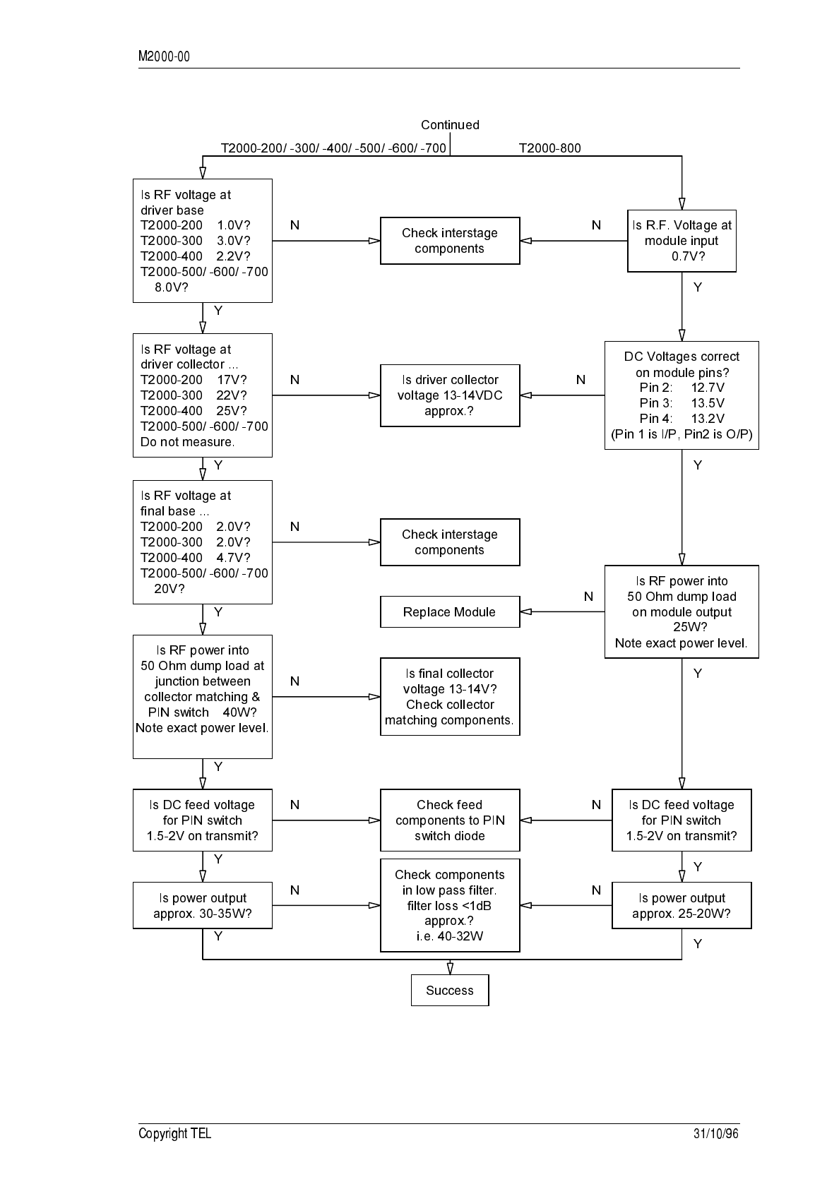
+80
≥
≥
≥
≥
≥
≥
≥
≥
≥
≥
≥
≥
≥
≥
≥
≥
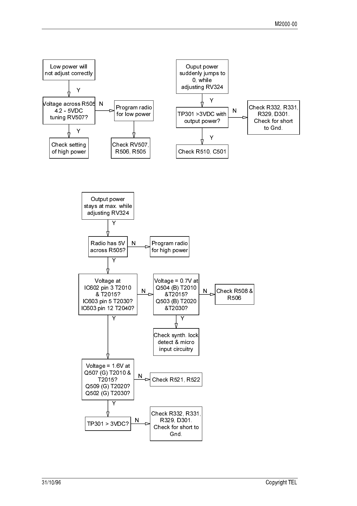
+8 1
+8180 7)3
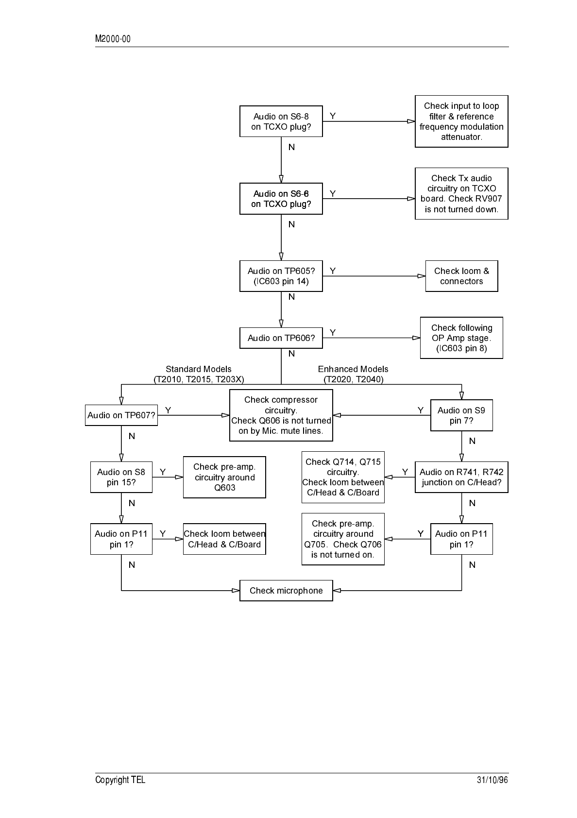
+8
+8181 !!
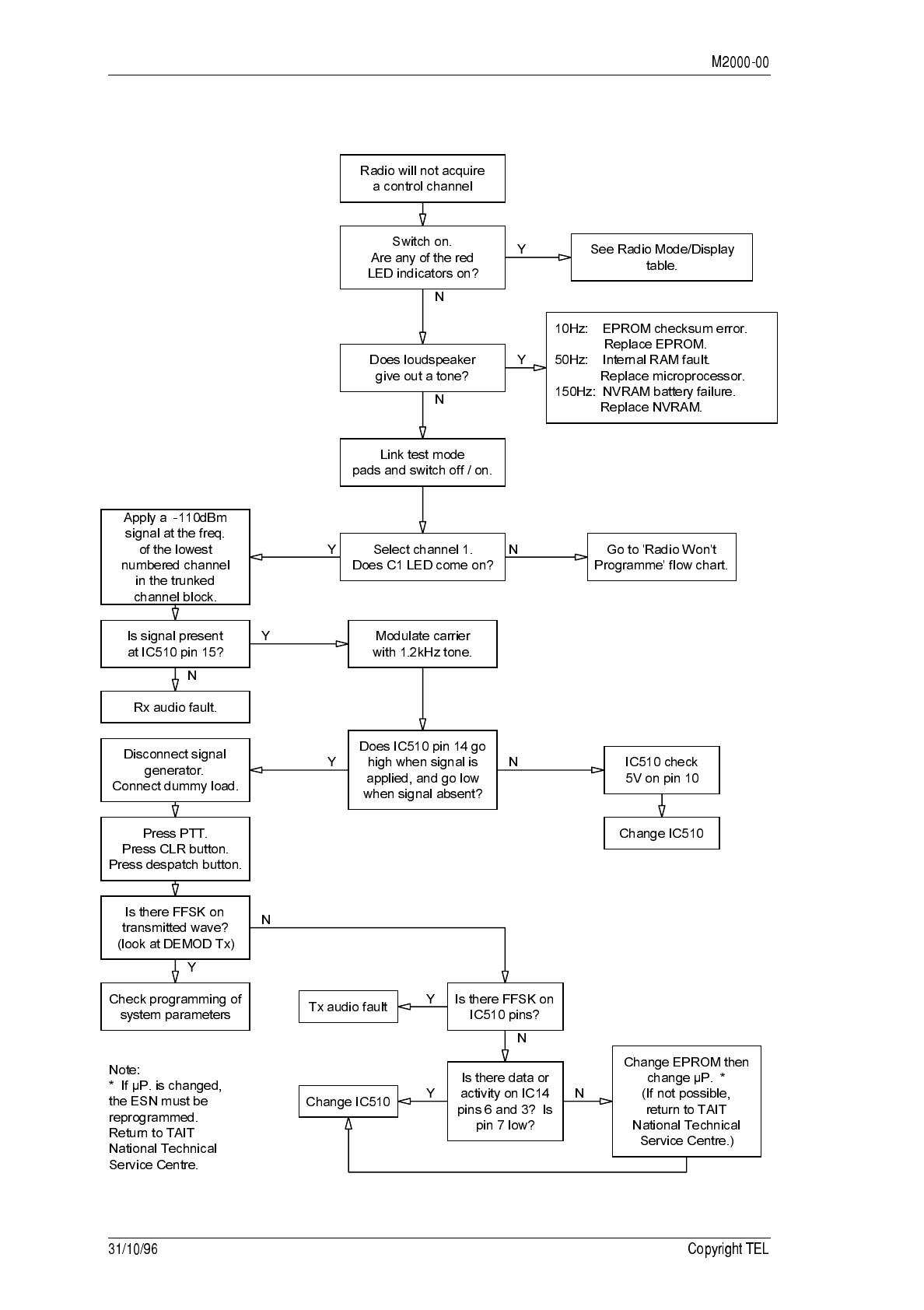
+8
+818 9BD!#(!))

! -8
-
4!5
This Section details procedures for tuning and adjustment of T2000 series II radios. This
is normally only required during product manufacture or after major servicing.
The following topics are covered in this Section:
Section Title Page
6.1 Tuning Precautions 6.2
6.2 Tuning & Adjustment Points 6.3
6.3 Trunked Radios 6.5
6.4 Transmitter Adjustments 6.5
6.4.1
6.4.2
6.4.3
6.4.4
6.4.7
6.4.5
6.4.7
6.4.8
6.4.8.1
6.4.8.2
Power Output
TCXO Alignment
Dual Point Modulation Adjustment
CTCSS Modulation Adjustment
Modulation Adjustment
LTR Code Deviation Adjustment
Selcall Tone Deviation
FFSK Adjustment (Trunked Models Only)
T203X Radios
T2040 Radios
6.5
6.6
6.6
6.7
6.7
6.7
6.7
6.8
6.8
6.8
6.5 Receiver Adjustments 6.9
6.5.1
6.5.2
6.5.3
6.5.3.1
RF Alignment
Internal Mute Control
RSSI
‘L’ Level Set-Up (Trunked Radios Only)
6.9
6.10
6.10
6.10

-8 !
-8 #
Refer to Section 4.1 for a list of test equipment required and a suggested test set-up. The
following precautions must be observed when carrying out the alignment procedures in
this Section.
• The microprocessor shield must remain in place throughout the alignment proce-
dure, with its 3 retaining screws torqued down to 8in.lbf (0.9Nm).
To gain access to the alignment test points and adjustment controls, it is only neces-
sary to remove the top cover and logic PCB mounting screws (refer to Section 3.2.1).
• For accurate tuning, the test cable connecting the signal generator or power meter to
the T2000 must be as short as practical and fitted with a ‘mating’ BNC connector.
Do not use adaptors, ‘sniffer’ couplings, etc., which introduce changes to cable
impedance and errors in test results.
• Non-metallic tuning tools must be used for the alignment of all coil slugs. The use of
metallic tools will result in tuning errors.
Tuning tools need to be of correct size to avoid the damage to coil slugs.
• The RF PA and audio output IC have a direct unswitched supply, and are therefore
not controlled by the control head on/off switch. This switch removes power only
from the regulated supplies.
) Under certain circumstances the microprocessor can key the transmitter.
Ensure that all instruments are protected from accidental PTT at all times.
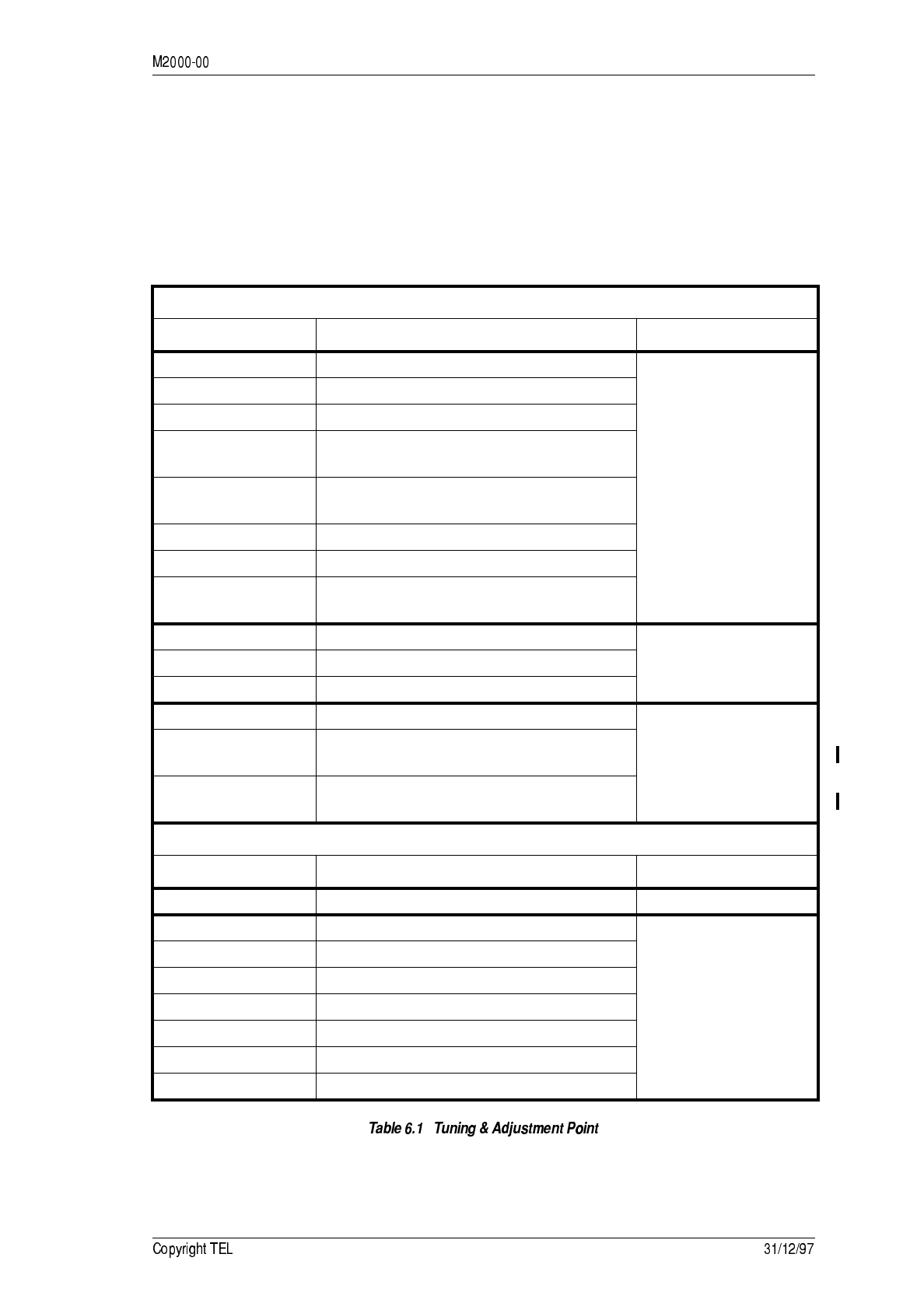
! -8
-8 4!5
The following table lists tuning and adjustment points, and Figure 6.1 shows their posi-
tion on the RF and TCXO/Tx audio PCBs.
The PCB layouts in Section 7 have all relevant logic PCB test and adjustment points
marked.
Tuning/Adjustment Point:
Designator Function Location
RV153 internal squelch control
RF PCB
RV222 dual point modulation control
RV324 high power control
CV212 x4 multiplier
(only used in T2000-800)
L104 to L106 front end tuning
(not used in T2000-800)
L114 & L116 IF tuning
L119 quad coil
L203 x3 /x4 multiplier
(not used in T2000-200)
RV906 CTCSS deviation control TCXO/Tx audio PCBRV907 deviation control
RV923 frequency control
RV507 low power control
logic PCB
#RV508 T2010, T2015 & T2020:
signalling adjust (not fitted as standard)
#RV599 T203X, T2040, T2050 & T2060:
FFSK adjust
Test Points:
Designator Function Location
TSP901 dual point modulation test point TCXO/Tx audio PCB
TP601 Rx audio (detected)
logic PCB
TP602 Tx CTCSS
TP603 Rx CTCSS
TP604 Rx audio
TP605 Tx audio
TP606 ALC audio
TP607 pre-amp output
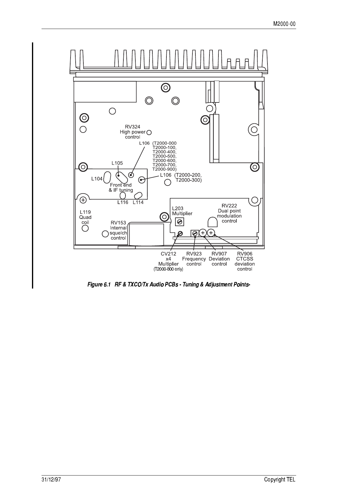
-8" !
! -8+
-8 9
The ‘test’ facility enables T2000 trunked radios to emulate a multichannel radio, using
the frequencies reserved for trunking.
For a description of how to put the radio in test mode, refer to Section 5.8 “Trunked
Radios: Test Mode”. Once the radio is in test mode, tuning and adjustment can be car-
ried out as described in Section 6.4 and Section 6.5.
) When in test mode, connect the antenna socket to a dummy load to pre-
vent interference with trunking systems. Avoid testing on channels in use
locally.
-8" !5
In this Section, deviation settings are given first for wide band, followed by settings for
medium band in brackets ( ) and settings for narrow band in square brackets [ ].
-8"8 7*&
Set up the test equipment as shown in Section 4, and close the PTT switch.
Turn RV324 fully clockwise and check that the output power is greater than 30W
for all channels.
Select a channel programmed for high power and adjust RV324 for 25W.
Check that the transmit current is approximately the values stated below:
Select a channel programmed for low power and adjust RV507 for the required
output power.
Model Current
T2000-100 6A
T2000-200 6A
T2000-300 6A
T2000-400 6A
T2000-500 6.5A
T2000-600 7A
T2000-700/900 6.5A
T2000-800 6A

-8- !
-8"8 );*!
Close the PTT switch and monitor the transmit frequency with a frequency coun-
ter.
Adjust RV923 on the TCXO/Tx audio PCB for a channel frequency within ±100Hz
at ambient temperature.
-8"8 !5
DC isolate the audio generator from TSP901 using a capacitor (10µF is sufficient).
Set the audio generator to 7kHz and inject the audio into the dual point modula-
tion input TSP901 on the TCXO/Tx audio PCB.
Close the PTT switch and select the lowest frequency channel.
Adjust the audio generator level to give a reading of ±5.2kHz deviation on the
modulation meter.
Remove any filters selected on the deviation or modulation meter which could
give erroneous readings.
Select the highest frequency channel and check that the deviation is ±4.8kHz.
If not, adjust the audio generator output level so that the average deviation of the
two channels is ±5kHz.
The difference in deviation between the two channels must be less than
±800Hz.
Select the lowest frequency channel, set the audio generator to 70Hz and inject
the audio at TSP901.
Adjust RV222 to give ±4.8kHz deviation on the modulation meter.
Select the highest frequency channel and check that the deviation is ±5.2kHz.
If not, adjust RV222 so that the average deviation of the two channels is ±5kHz.
The difference in deviation between the two channels must be less than
±400Hz.

! -8.
-8"8" ))!5
The following instructions apply only to those radios with CTCSS activated and
must be carried out before any further modulation adjustment can proceed.
Refer to the T2000 Programming Manual for the CTCSS channel programming
instructions. The frequency range of the CTCSS tone is 67 to 250.3Hz.
Switch to any channel with CTCSS activated.
Close the PTT switch.
Adjust RV906, on the TCXO PCB, to set the CTCSS tone peak deviation for
±660Hz ±100Hz (±530Hz ±80Hz) [±330Hz ±50Hz] on the modulation meter.
-8"8+ ,)!5
Close the PTT switch and set up a continuous call. This can be an LTR Repeater
Talkaround call, a Repeater Interconnect Call (RIC) or an on-channel call.
Adjust RV906 on the TCXO PCB to set the LTR code deviation to ±1kHz (±900Hz)
[±600Hz].
A The deviation meter must have a good low frequency response to avoid incor-
rect readings.
-8"8- !5
Complete the dual point modulation and CTCSS modulation adjustments (Sec-
tion 6.4.3 and Section 6.4.4) before commencing the modulation adjustment.
Apply a 3kHz sine wave at a level of -40dBm to the microphone input.
Select a channel with CTCSS activated and close the PTT switch. If CTCSS is disa-
bled, select any channel.
Adjust RV907 for a +5kHz (+4kHz) [+2.5kHz] deviation reading on the modula-
tion meter.
Maintain the same sine wave output level and sweep the audio frequency from
300Hz to 3.3kHz.
Find the frequency of maximum ‘+’ deviation and readjust RV907 for +5kHz
(+4kHz) [+2.5kHz] deviation.
Reset the modulation meter to read ‘-’ deviation.
Slowly sweep the audio frequency from 300Hz to 3kHz. If the ‘-’ deviation peak is
found to exceed -5kHz (-4kHz) [-2.5kHz], readjust RV907 for a peak deviation of
-5kHz (-4kHz) [-2.5kHz] at that frequency.
The peak deviation should not exceed ±5kHz (±4kHz) [±2.5kHz] on any channel.

-8/ !
-8"8. #
This is normally preset at 60% of voice deviation. If adjustment is needed, fit
#RV508 (refer to Section 7 for a component description) to the logic PCB, and pro-
ceed as follows.
Adjust #RV508 for ±3kHz (±2.4kHz) [±1.5kHz] deviation reading on the modula-
tion meter.
Check to ensure that no limiting occurs in IC901.
-8"8/ 33E!5>9*?
-8"8/8 1 ;
Enter test mode (refer to Section 5.8, “Trunked Radios: Test Mode”).
Press the front panel # key .
Adjust #RV599 for ±3kHz ±200Hz (±2.4kHz ±160Hz) [±1.5kHz ±100Hz] deviation
reading on the modulation meter.
-8"8/8 1"1
Enter test mode (refer to Section 5.8, “Trunked Radios: Test Mode”).
Select test function 10 using the control head.
Adjust #RV599 for ±3kHz ±200Hz (±2.4kHz ±160Hz) [±1.5kHz ±100Hz] deviation
reading on the modulation meter.
2
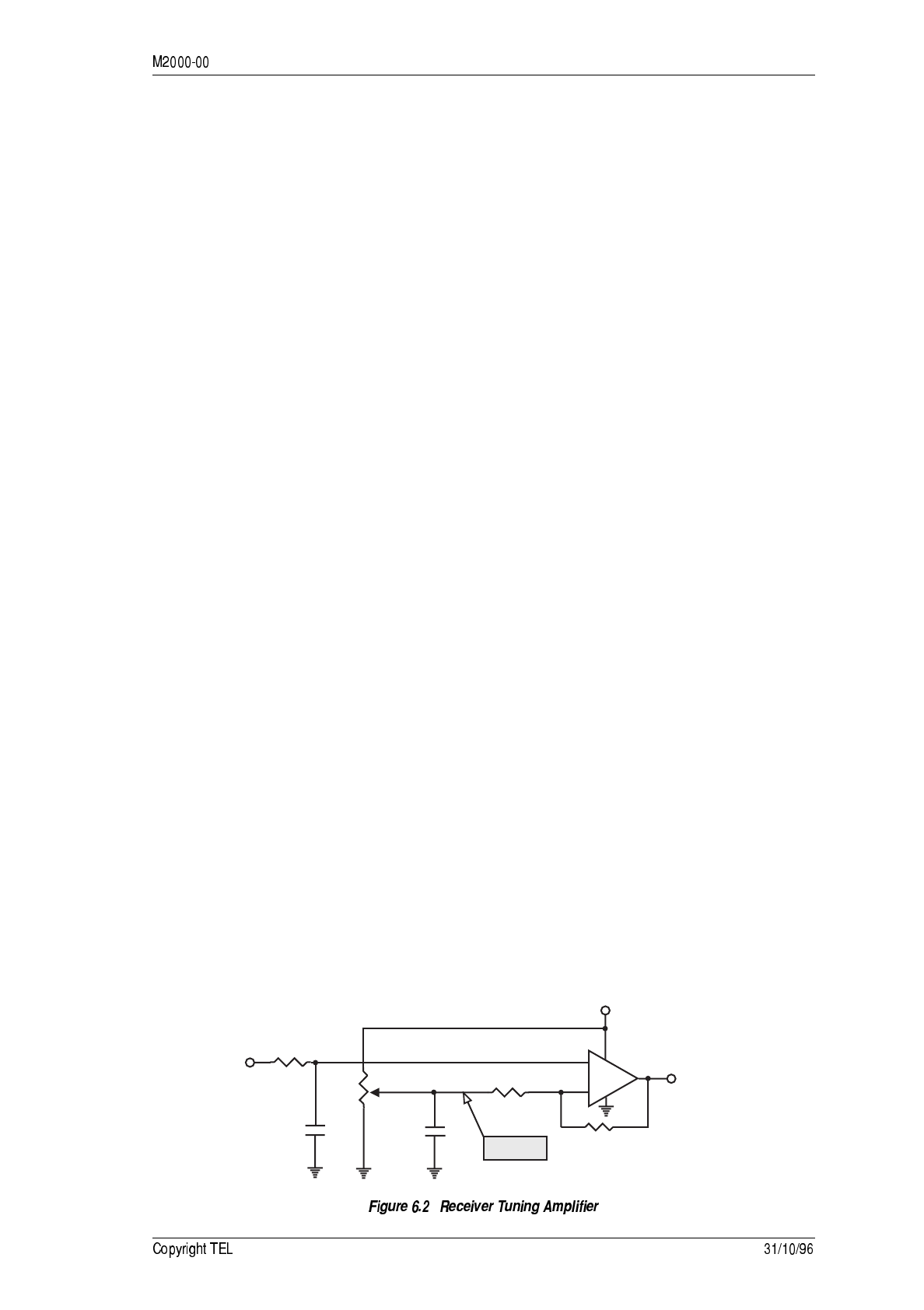
! -80
-8+ #!5
In this Section, deviation settings are given first for wide band, followed by settings for
medium band in brackets ( ) and settings for narrow band in square brackets [ ].
-8+8 3!
Set up the test equipment as shown in Section 4, and select the highest possible
frequency in the operating band.
Set the signal generator to the required receive frequency with modulation set for
±3kHz (±2.4kHz) [±1.5kHz] deviation at 1kHz AF and an output level of
-100dBm.
Using the receiver tuning amplifier circuit shown in Figure 6.2, adjust RV1 until
the voltage of point A equals 3.0V DC, measured on a 1MΩ digital multimeter.
Connect the receiver tuning amplifier to the RSSI output on pin 15 of S14 (logic
PCB) and monitor the output on an oscilloscope (1V/division, DC coupled).
If the output on the oscilloscope is 0V DC, increase the RF input level above
-100dBm until the output level just starts to rise.
Adjust L104, L106, L105, L114, L116 and L203, in this order, to give maximum
amplitude.
A L203 is not used in the T2000-200.
While tuning the coils, adjust the signal generator output so that the level on the
oscilloscope does not exceed 6V DC.
Monitor the audio output at the speaker terminals and adjust L119 for maximum
amplitude.
Set the squelch control (RV153) to minimum and connect a sinad meter across the
speaker terminals.
Decrease the signal generator output until a 12dB sinad is reached.
The signal generator output should not be greater than -117dBm.
Switch to the lowest possible frequency in the operating band, and check that the
receiver sensitivity is better than -117dBm.
C2
1µF
R3
10k
RV1
100k
(26 turn)
IC1
LM358
1
2
3
+
-
R1
12k
input
f
rom
RSSI
R2
390k
+9V DC
output to
oscilloscope
1V/div.
(DC coupled)
C1
1µF
++
A = 3V DC

-81 !
-8+8 $)
If required, the mute setting can be adjusted internally as follows.
Align the receiver, as described in Section 6.5.1.
Adjust RV153 fully clockwise.
Set the signal generator to the required receive frequency.
Set the modulation for ±3kHz (±2.4kHz) [±1.5kHz] deviation at 1kHz AF.
Adjust the signal generator output for 11dB sinad.
Adjust RV153 so that the radio mutes then turn RV153 until the mute gate just
opens.
-8+8 $
The T2000 RSSI is non-adjustable and should operate over an approximate 50dB
range.
Monitor the RSSI output on pin 15 of S14 on the logic PCB.
Set the signal generator to the required receive frequency with modulation set for
±3kHz (±2.4kHz) [±1.5kHz] deviation at 1kHz AF and an output level of -70dBm.
Decrease the signal generator output in 10dB steps to -120dBm, noting the RSSI
output at each step.
The RSSI should have a typical slope of approximately 540mV/10dB, from
-120dBm to -70dBm RF input.
-8+8 8 F,D,%&>9*?
These levels are factory set at the time of manufacture and will require reprogram-
ming only if the receiver has been realigned or has had parts replaced, or if the
logic PCB has been replaced.
Set the signal generator to give an unmodulated RF signal in the centre of the
trunking band.
Enter test mode.
A The T203X will need to use CCTM, as described in Section 5.8.3.
Set the signal generator to -108dBm and program ‘L1’ (function 61), as described
in Section 5.8.5.2.
Set the signal generator to -100dBm and program ‘L2’ (function 62), as described
in Section 5.8.5.2.