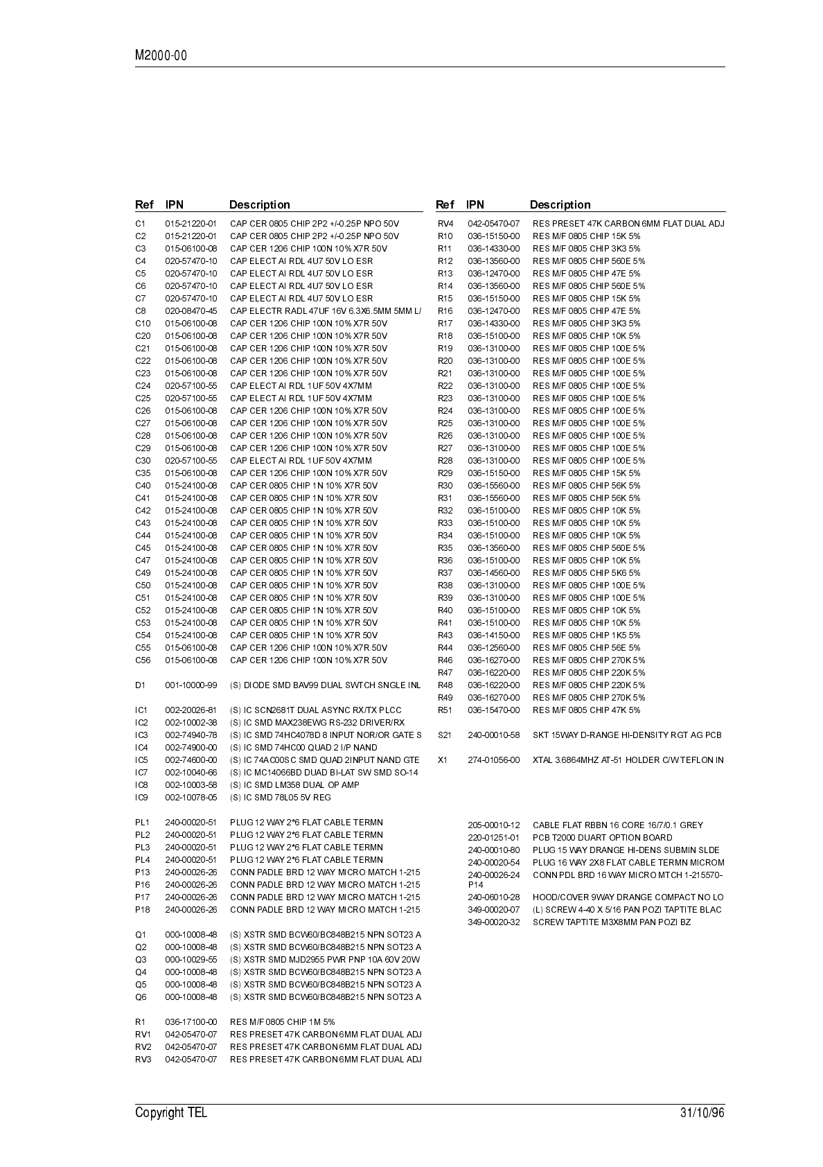
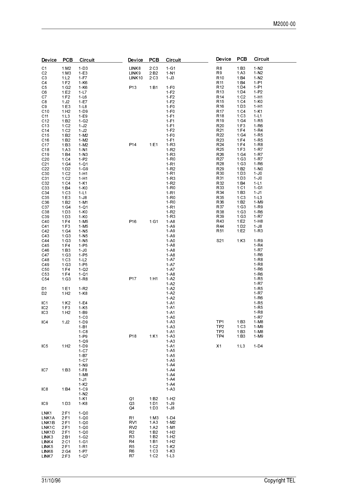
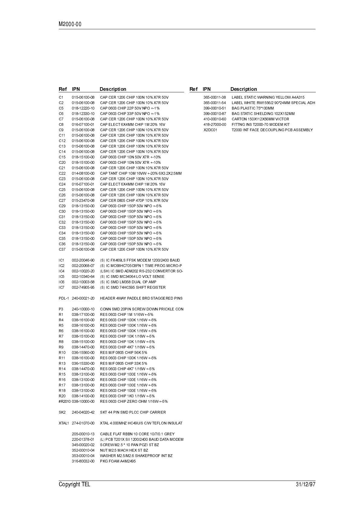
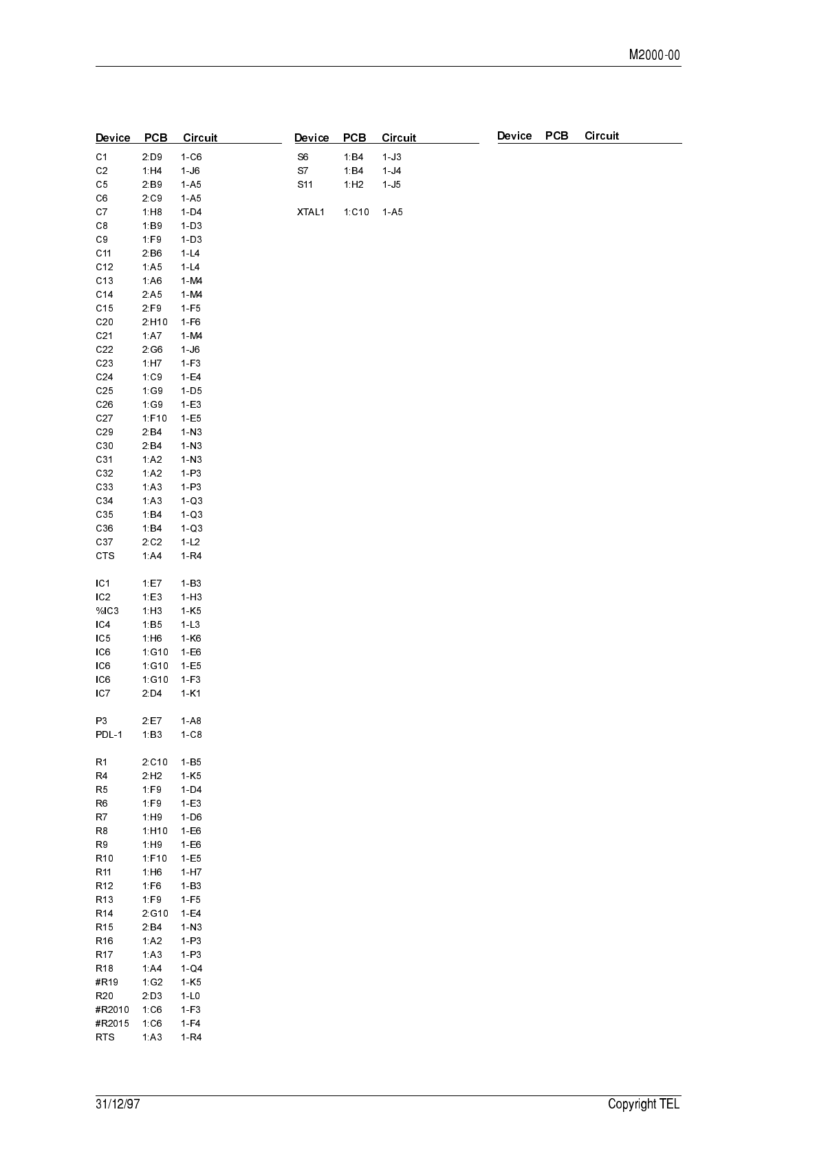
Contents
user manual part 6

!4&)
;*74)?
The T2000-60 dual port UART Interface Module (UIM) allows computer control of a
T2020 or T2040 Series II radio. With full remote control, either semi or fully automatic
communication systems can be developed.
The UIM requires radio software Version 2.XX, and to program the UIM param-
eters, the programming software must be PGM2000 Release 7, or later.
The T2020 and T2040 use Tait’s proprietary radio software protocol. For detailed
information regarding this protocol, refer to the UART Applications Manual, or
contact your local Tait dealer.
The following topics are covered in this Section:
Section Title Page
8.12.1 Components Required 8.12.2
8.12.2 Fitting 8.12.3
8.12.3 T2000-60 Link Options 8.12.4
8.12.4 T2000-60 Set-Up 8.12.5
8.12.5 Signal Specifications 8.12.7
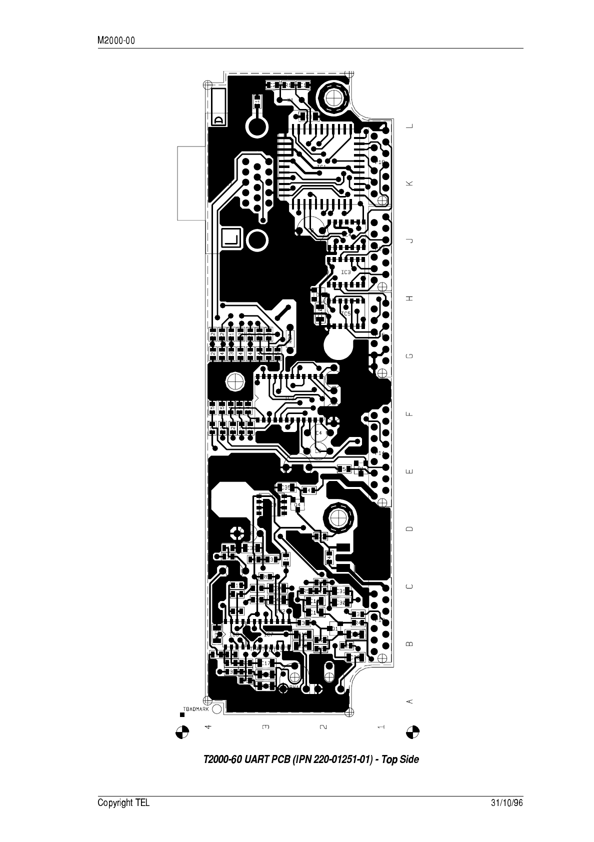
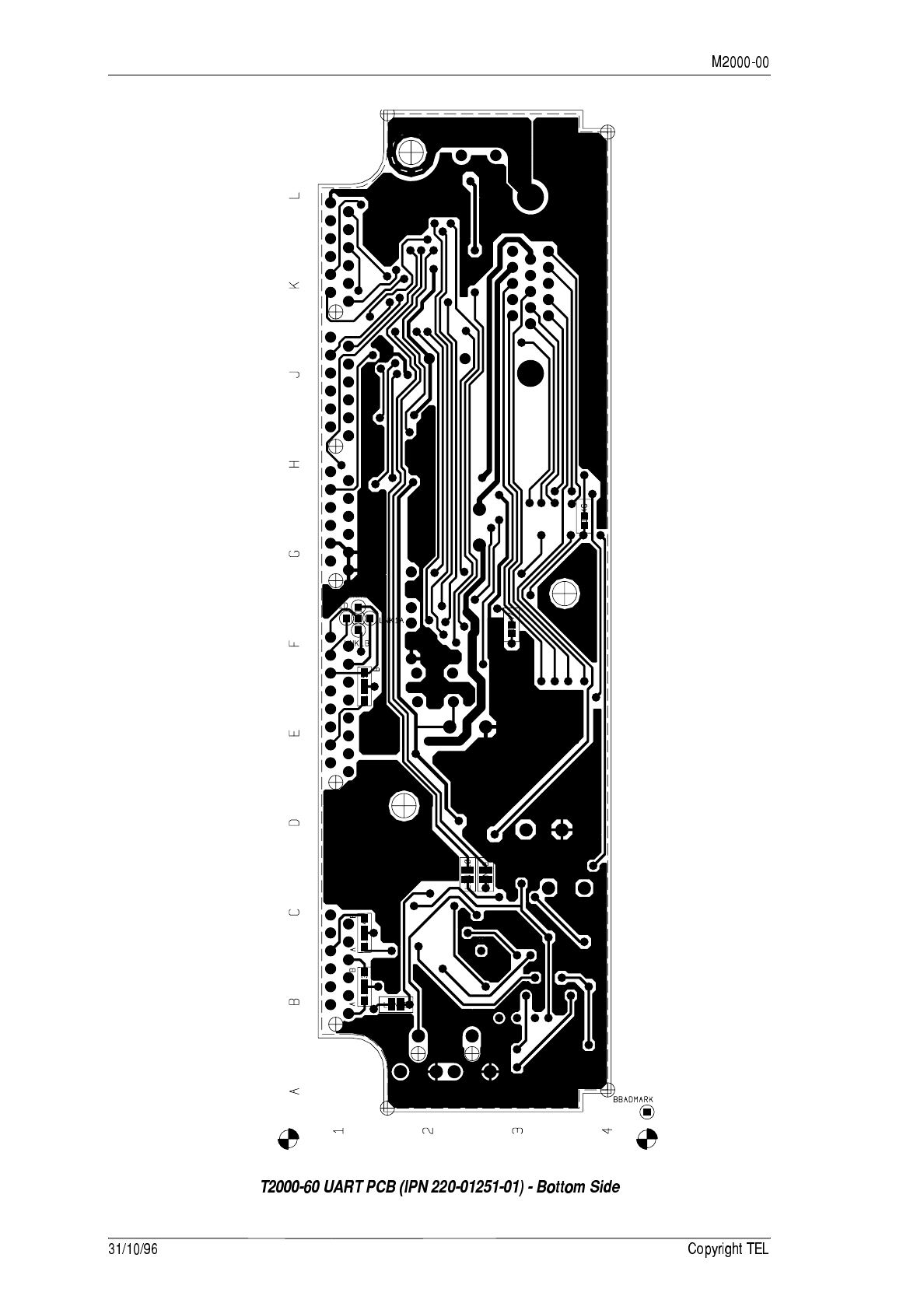
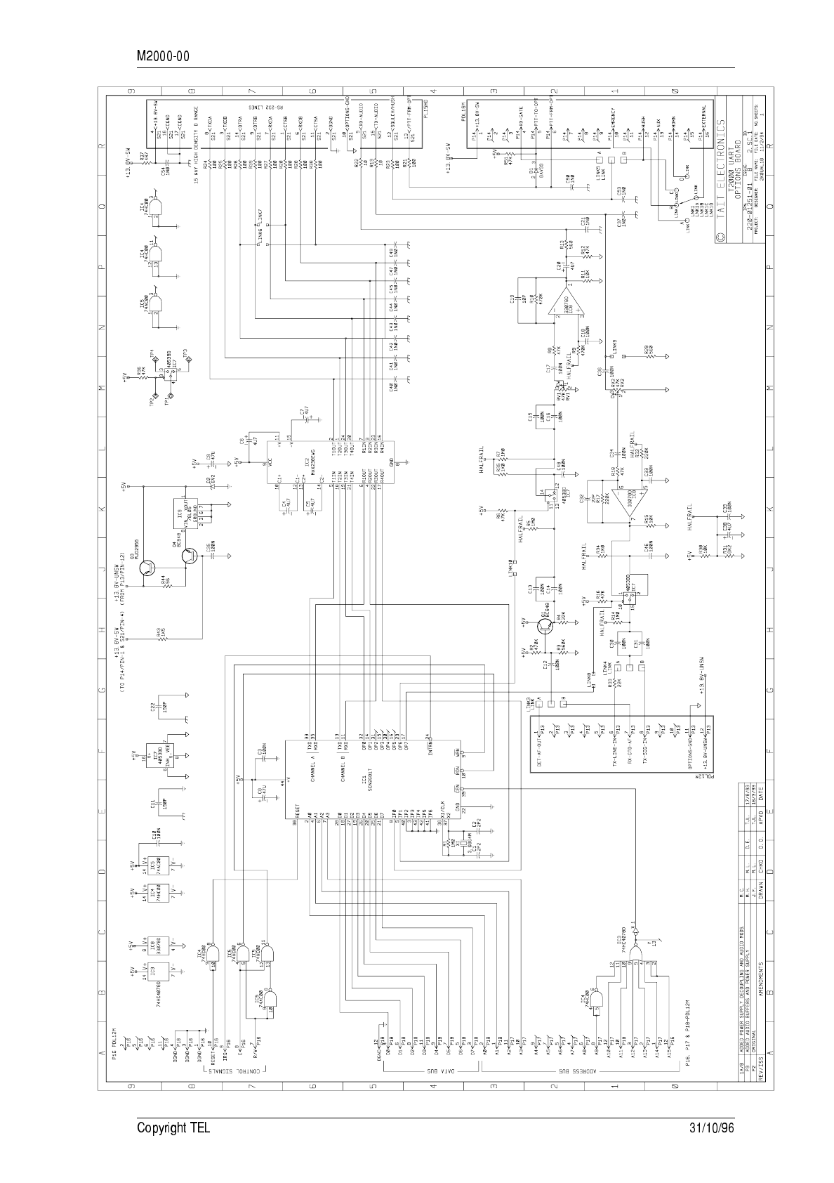
8.12.6 PCB Information 8.12.9
!4&)
!)6(
The T2000-60 kit contains the following components:
(7
T2000-60 Applications Manual IPN 408-20060-0X.
!33,
UIM Uart Interface Module
CE Computer Equipment
AE Auxiliary Equipment
Refer to the Applications Manual for details on the interaction of CE to AE with the
UIM.
Quantity Description
1 T2000-60 UART PCB assembly
1 15-way high density D-range plug
1 shroud (alternative shroud - not required for T2000 Series II radios)
3 M3x8 pan Pozi Taptite screws
2 4-40x¼ pan Pozi Taptite screws (black)
!4&)
.
&
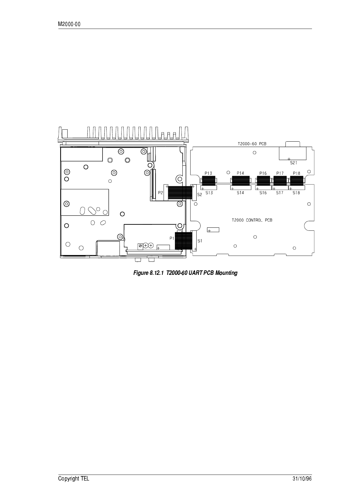
1Refer to Figure 8.12.1.
Remove the top cover of the radio by unscrewing the four cover screws, remove
the D-range blanking plate in the rear of the T2000 radio, unscrew the logic PCB
and fold-out.
Position the UIM PCB as shown, and connect the Micromatch connectors P13, P14,
P16, P17 and P18 to S13, S14, S16, S17 and S18 on the T2000 logic PCB.
2Set up the UIM, as described in Section 8.12.4.
3Carefully fold the logic and UIM PCBs back in position, guiding the D-range con-
nector through the hole provided in the T2000 chassis.
Secure using the three logic PCB retaining screws and the three M3x8 screws pro-
vided and refit the top cover.
Plug the D-range assembly provided in the kit into the D-range connector (S21).
Holes are provided in the T2000 chassis for the D-range plug locking screws.
Use the two black 4-40 Taptite screws provided in the kit to form the threads.
!4&)
;*#8
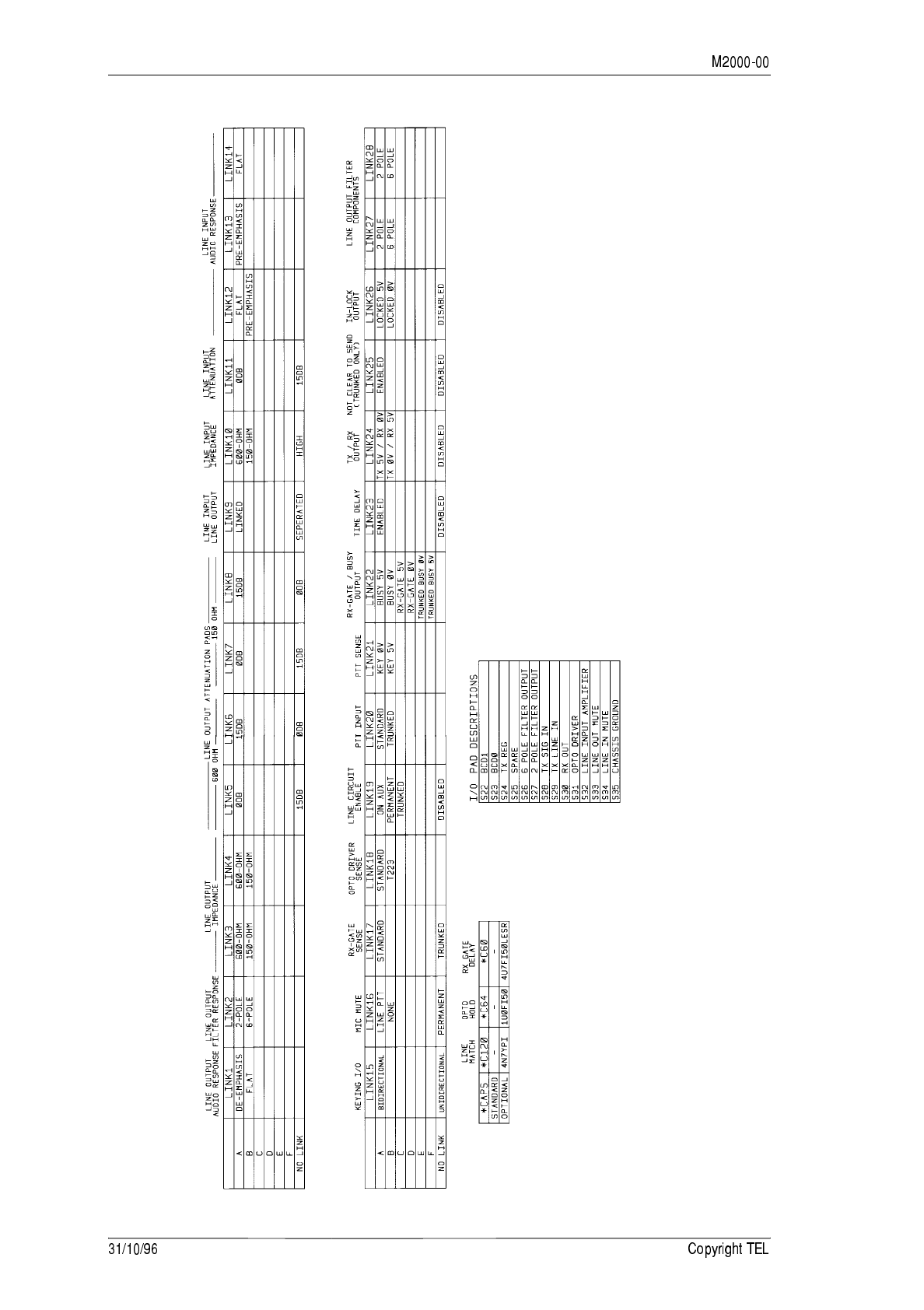
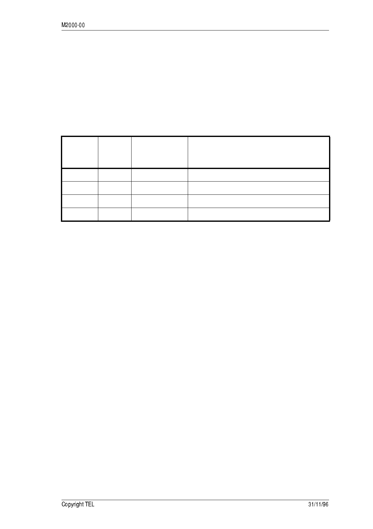
Provision has been made on the T2000-60 PCB for different application requirements.
The PCB links are either solder shorted or fitted with 0Ω SMD resistors.
The following table sets out the linking options on the T2000-60 UART PCB.
This table refers only to T2000-60 issue 01 (i.e. PCB IPN 220-01251-01), or later.
For a description of how to identify PCBs, refer to “PCB Identification”, on page
7.2
* The analogue signals provided by the UIM must be set up according to the
requirements of the AE (bearing in mind the UIM maximum output levels).
Link Option
CE controlling radio with AE fitted*CE controlling radio with no AE fitted
LINK1
LINK3A non-processed audio
(DET-AF-OUT connected to RX-AUDIO)
LINK3B processed audio (de-emphasised)
(RX-GTD-AF connected to RX-AUDIO2)
LINK4A processed audio (pre-emphasised)
(TX-AUDIO connected to TX-LINE-IN)
LINK4B non-processed audio
(TX-AUDIO connected to TX-SIG-IN)
LINK5A T2020
(SQULCH/HUSH to RX-GATE)
LINK5B T2040
(SQULCH/HUSHconnected to HUSH)
LINK6 no handshaking required
LINK7 no handshaking required
LINK8 normal operation
(removal of this link disables the audio mute)
LINK9 normal operation
(this link provides a line termination resistor)
LINK10 normal operation
(removal of this link disables the audio mute)
!4&)
;*;4
56)6(
• AF signal generator
• modulation analyser
• high impedance voltmeter (e.g. VTVM)
• IBM† or compatible personal computer
• lead to connect radio to CE and AE, if required (refer to Figure 8.12.2 & Figure 8.12.3)
• oscilloscope
• power supply (+13.8V)
• RF signal generator
• 40dB RF attenuator
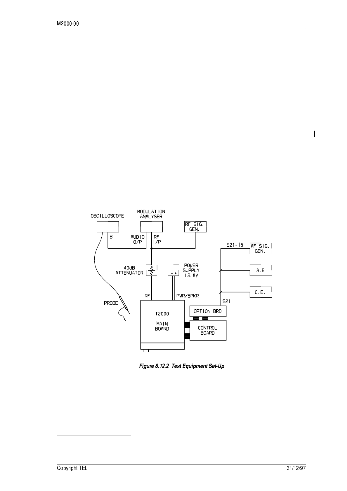
The following diagram shows a typical test set-up.
† IBM is the registered trademark of International Business Machines.

* !4&)
)=(#,
1Set up the test equipment as shown.
2Ensure that pin 5 of S21 is loaded with the impedance normally presented by the
AE (typically 600Ω).
3Apply an RF signal at a level of -50dBm on an appropriate channel. Internal mod-
ulation at 1kHz should be enabled, with the deviation set to ±1.5kHz for a narrow
band radio and ±3kHz for a wide band radio.
If CTCSS or Selcall is enabled, ensure that the signalling mutes are overridden
(for T2040 radios, refer to Section 5.8.5, “Test Facilities Available”).
4Connect the scope probe to pin 5 of S21, and adjust RV1 to the level required by
the AE.
=(#,
1Set up the test equipment as shown.
2Connect a 600Ω impedance AF signal generator to pin 15 of S21. If the internal
impedance of the AE is not 600Ω, either load the AF signal generator to get an
internal impedance equivalent to the AE or alternatively, use the AE to provide
the test signal (this is possible with most packet radio modems).
3Apply an audio test signal to TX-AUDIO and set the radio to transmit (for T2040
radios, refer to Section 5.8.5, “Test Facilities Available”).
4Connect the scope probe to pin 15 of S21 and adjust the AF signal generator to a
frequency of 1kHz at a level of 700mVp-p.
While the radio is transmitting, adjust RV2 to produce a deviation on the modula-
tion analyser as stipulated by the AE.
If you are using the test signal from the AE instead of the AF signal generator,
there will be some means of adjusting the signal level inside the AE.
!4&) +
&
The following table describes the electrical specification of all CCI interface signals.
These signals are available at the 15 way high density D-type connector (S21) mounted
on the heatsink at the rear of the radio.
All signals necessary to provide CE and modem connection may be routed via these
pins. Some signals may be selected by links on the UART interface module for different
characteristics (refer to the circuit diagram and Section 8.12.4).
S21
Pin No. Signal Description
1CTSB Clear to send in B
Handshaking input for port B. This signal complies with the
electrical requirements of the RS-232 specification.
2DGND Digital ground
Ground reference for all digital signals.
3TXDB Transmit data out port B
Data output from serial port B. This signal complies with the
electrical requirements of the RS-232 specification.
4 +13.8V-SW +13.8V supply out
Switched supply voltage. Can supply power to the AE when
the radio is switched on. Maximum current = 300mA.
5 RX-AUDIO Receive audio out
This output is link selectable between one of the following sig-
nals:
1. DET-AF-OUT
(P13 pin 1) Receiver detected audio: unprocessed
receiver audio.
Output impedance = 600Ω
.
Delivers 0 to 250mVrms (adjustable) into
600Ω at 1kHz (60% of full system deviation).
2. RX-GTD-AF
(P13 pin 7) Receiver gated audio: de-emphasised
receiver audio, gated by mute element.
Delivers 0 to 250mVrms (adjustable) into
600Ω at 1kHz (60% of full system deviation).
6RXDB Receive data in port B
Data input to serial port B. This signal complies with the electri-
cal requirements of the RS-232 specification.
7RXDA Receive data in port A
Data input to serial port A. This signal complies with the elec-
trical requirements of the RS-232 specification.
8TXDA Transmit data out port A
Data output from serial port A. This signal complies with the
electrical requirements of the RS-232 specification.
9DTRB Data terminal ready out B
Handshaking output for port B. This signal complies with the
electrical requirements of the RS-232 specification.
10 OPTIONS-GND Options ground
Ground reference for all analogue signals.
!4&)
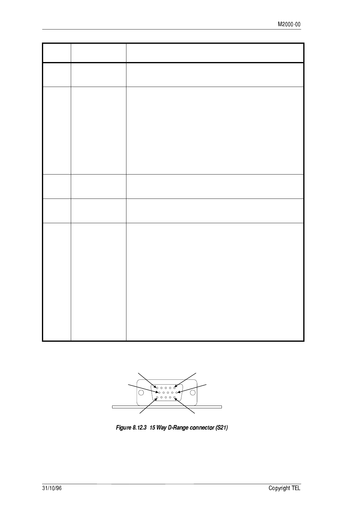
The following diagram shows the pin designations of S21, viewed from the rear of the
radio.
11 CTSA Clear to send in A
Handshaking input for port A. This signal complies with the
electrical requirements of the RS-232 specification.
12 SQULCH/HUSH Auxiliary output: receiver audio valid
Signal indicates valid audio is being output from RX-AUDIO.
This output is link selectable between the following signals:
1. RX-GATE
(P14 pin 4) Receiver Gate: received audio mute control
line.
Logic high = muted.
5V CMOS logic.
2. HUSH
(P14 pin 12) External Device Mute: controls muting of
an external device during radio activity.
Logic high = muted.
5V CMOS logic output.
13 /PTT-FRM-OPT Transmit request in
Press To Talk: active low transmit request input.
5V CMOS logic input.
14 DTRA Data terminal ready out A
Handshaking output for port A. This signal complies with the
electrical requirements of the RS-232 specification.
15 TX-AUDIO Transmit audio in
Audio input to the radio. This input is link selectible between
one of the following signals:
1. TX-SIG-IN
(P13 pin 8) Transmit signal: transmit audio input, post
processing.
Input impedance = 600Ω or high imped-
ance. Requires 250mVrms at 1kHz to pro-
duce 0 to 80% of full system deviation
(adjustable).
2. TX-LINE-IN
(P13 pin 6) Transmit audio: transmit audio input,
before pre-emphasis.
Input impedance = 600Ω or high imped-
ance. Requires 110mVrms at 1kHz to pro-
duce 0 to 80% of full system deviation
(adjustable).
S21
Pin No. Signal Description
51
10 6
1115
PCB
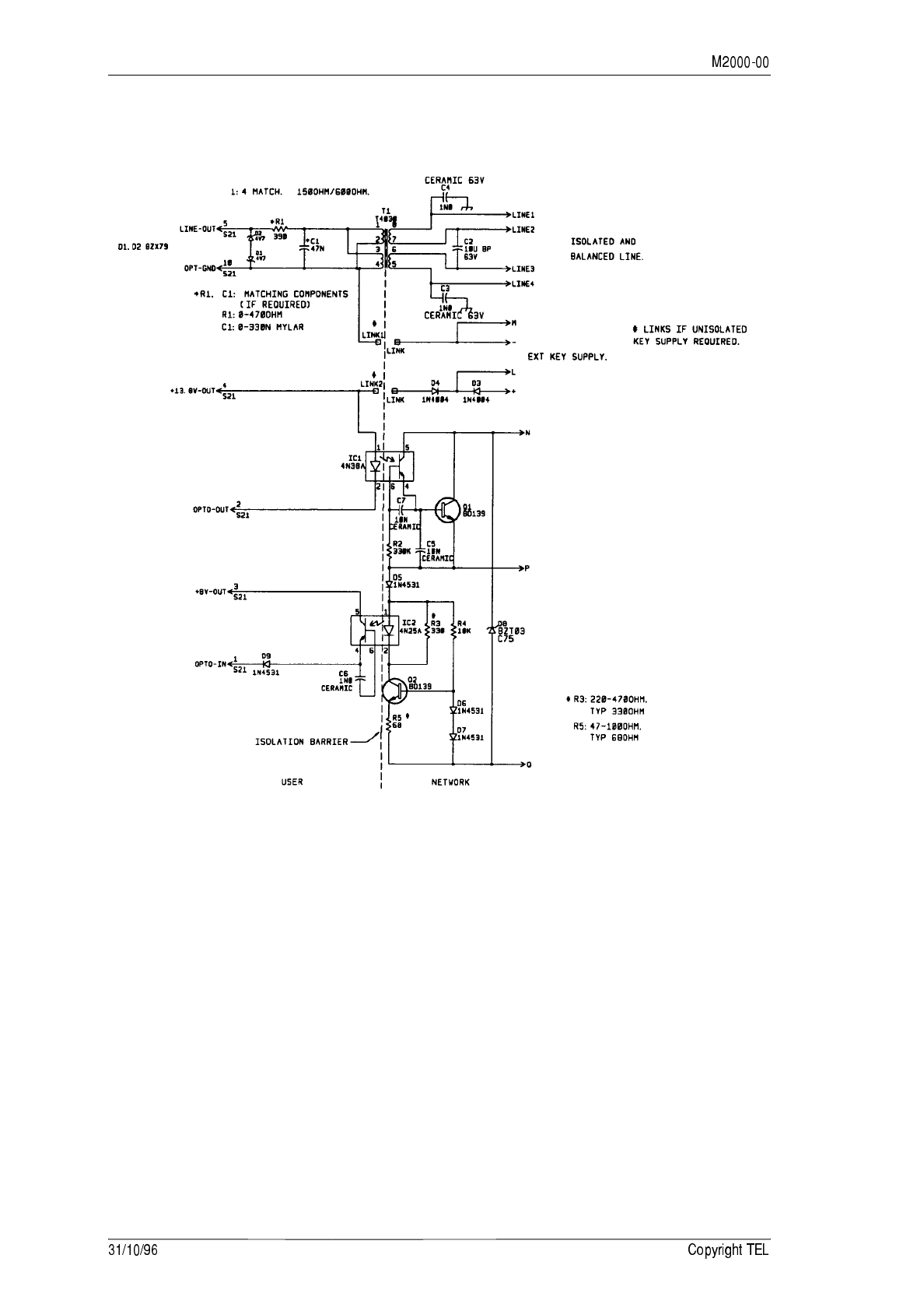
;*#0:; ;2
!4&) -
* !/
'$<'
!4&)
;*()(=0:; ;2
!4&)
!4&)
!4&)

!4&)
!!54&)
;**
&
4)?
The T2000-A66 single port UART kit allows computer control of a T2030, T2035 or T2040
Series II radio. With full remote control, either semi or fully automatic communication
systems can be developed.
The following topics are covered in this Section:
Section Title Page
8.13.1 Components Required 8.13.2
8.13.2 Fitting 8.13.2
8.13.3 Signal Specifications 8.13.3
8.13.4 PCB Information 8.13.4
!!54&)
!)6(
The T2000-A66 kit contains the following components:
.
&
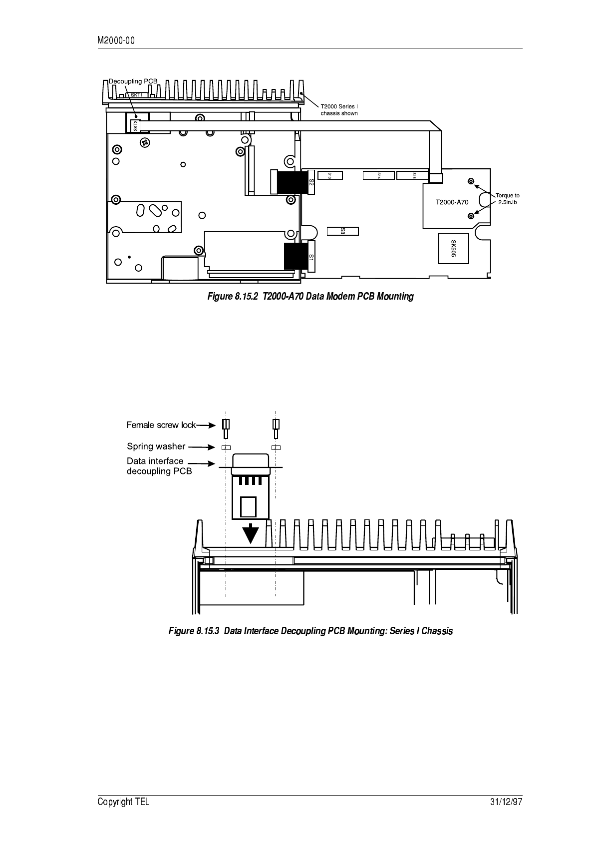
Refer to Figure 8.13.1.
1Remove the top cover of the radio by unscrewing the four cover screws, unclip the
D-range blanking plate in the rear of the T2000 radio, unscrew the logic PCB and
fold out.
2 T2000-A66 Mounting
Position the T2000-A66 PCB on the top side of the logic PCB, as shown, matching
P1 on the bottom side of the T2000-A66 PCB to the pads labelled ‘P1’ on the logic
PCB.
Use the two M2.5x10mm screws, nuts and shakeproof washers to secure in place.
The screws are fitted from the bottom of the logic PCB, and secured with the
nuts and washers on the top side of the UART PCB.
Torque the screws to 2.5in.lb. This ensures that the pressure connector, P1, makes
contact with the corresponding pads on the logic PCB.
Over-tightening the screws will cause the T2000-A66 PCB to bend, result-
ing in possible track damage.
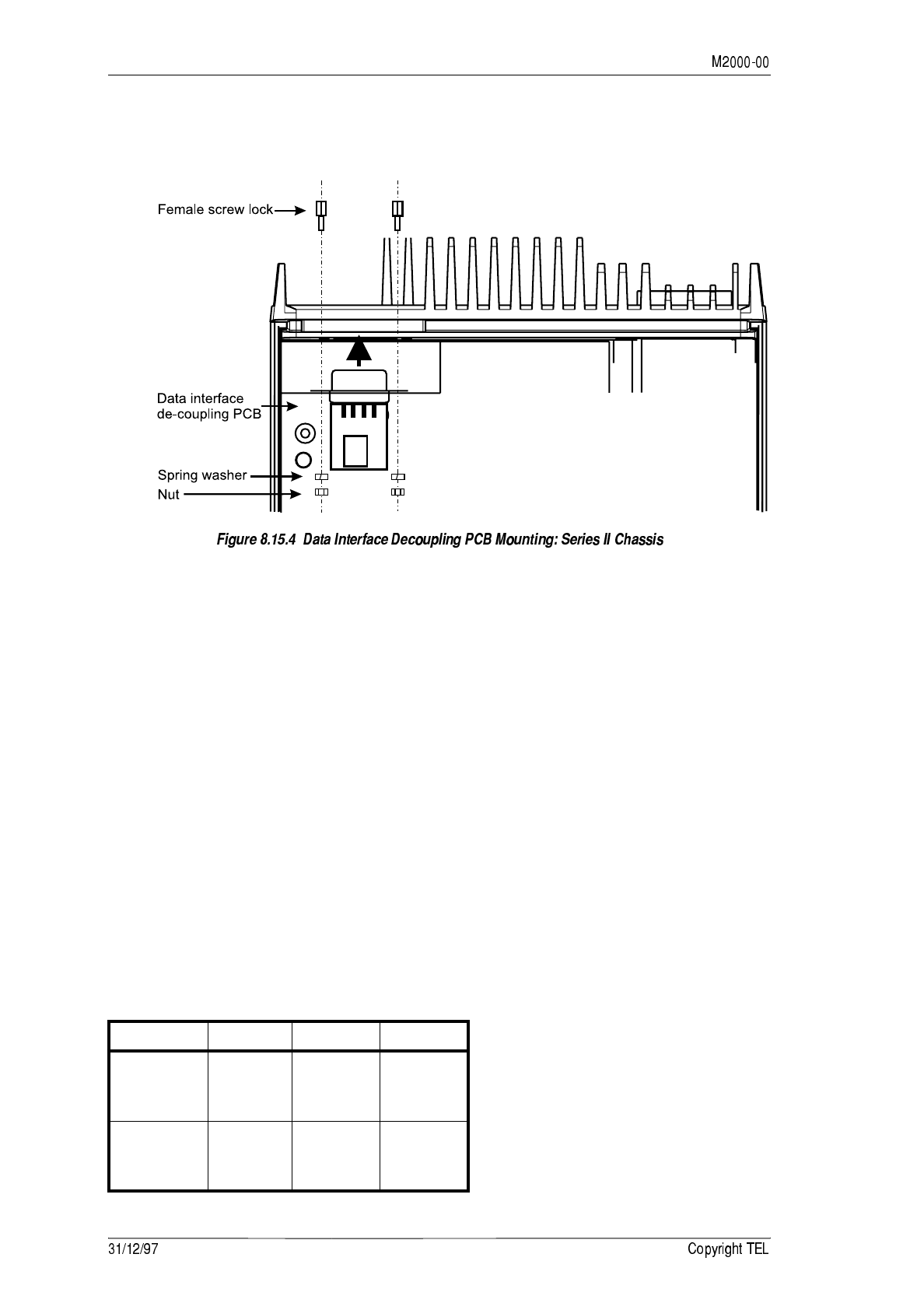
3 T2000 Data Interface Decoupling PCB Mounting
Fit the decoupling PCB to the T2000 chassis, guiding the PCB through the hole
provided.
Holes are provided in the T2000 chassis for the D-range locking screws. Use the
two black 4-40 Taptite screws provided in the kit to form threads.
Open the locking screw kit, discard the nuts, then secure the D-range using the
two locking screws and spring washers.
Quantity Description
1 T2000-A66 UART PCB assembly
1 Data Interface Decoupling PCB assembly (refer to Section 7.17)
2 M2.5x10mm pan Pozi Taptite screws
2 M2.5 shakeproof washers
2M2.5 nuts
1 locking screw kit (in plastic bag)
2 4-40x¼ pan Pozi Taptite screws (black)
20mm foam tape
1
!!54&)
4Fold the T2000-A66 loom as shown, then plug into SKT2 on the decoupling PCB.
5Fold the logic PCB back in position, and secure using the three logic PCB retaining
screws and refit the top cover.
&
The following table describes the signals used on the decoupling PCB 9 way D-range
connector (SKT1). The unused pins may be used for other signals, if required.
The following diagram shows the pin designations of SKT1, viewed from the rear of the
radio.
SKT1
Pin No. Signal Description
2TXDTransmit data: Serial data output from UART PCB. This signal complies
with the electrical requirement s of the RS-232 specification.
3RXDReceive data: Serial data input to UART PCB. This signal complies with
the electrical requirements of the RS-232 specification.
5DGNDDigital ground: Ground reference for all digital signals.
2
;**#0:;;2
!!54&)
!/
!!54&)
* !!54&)
!!54&) +
0
1
2
3
4
5
6
7
8
9
0
1
2
3
4
5
6
7
8
9
ABCDEFGHJ K
REV/ISS AMENDMENTS DATEAPVDD.O.CHKDDRAWN
NO.SHEETS:FILE NAME:
TAIT ELECTRONICS
IPN:
FILE DATE:
ISSUE: ID:.
2.SC.
PROJECT: DESIGNER:
1
2
T2000 SERIES 2
SINGLE PORT U.A.R.T
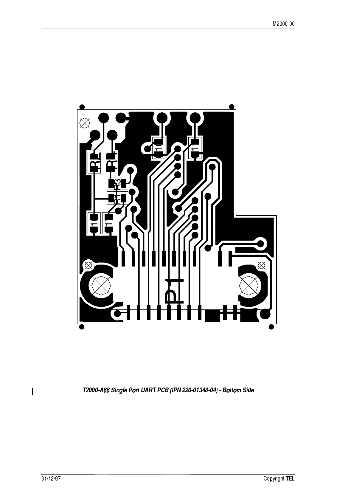
134804A
220-01348-04
17/12/96
4A
T2000 RPS
P1 NEW FOR SINGLE PORT OPTION ON T2000 CCB PW PW 27/06/95
1A CHANGED XTAL FOR SIDE MOUNT VER PW PW 28/08/95
2A ADDED SK3. CHANGED PLACEMENT TOE PW PW 05/03/96
3A NEW CONNECTOR. RELAY OF CCT DJW/RPS DJW 21/10/96
4A RELAY OF PCB RPS 17/12/96
C1
100N
C10
22P C11
22P
C12
100N
C13
100N
C14
100N
C15
100N
C16
1N0
C17
1N0
C2
100N
SCC2691
IC1
A2
6
A1
7
A0
8
D7
15
D6
16
D5
17
D4
18
D3
19
D2
20
D1
21
D0
22
MPI
5
GND
12
VCC
24
TXD 3
RXD 2
RESET 11
INTRN 13
CEN 14
RDN 1
WRN 23
X1 9
X2 10
MPO 4
IC2
MAX202
C1+
1
C1-
3
C2+
4
C2-
5
T2IN
10
T1IN
11
R1OUT
12
R2OUT
9
GND
15
+V
16
5/10+ 2
5/10- 6
T2OUT 7
T1OUT 14
R1IN 13
R2IN 8
R1
56
R2
56
R3
56
R4
56
P1
24WAY SKT
SK2
4 WAY PADDLE CONNECTOR
X1
3.6864M
S1
I/OPAD
SK2 DGND
1
SK2 DGND
4
SK2 RXD
3
SK2 TXD
2
+5V
+5V
+5V
P1
A1 5
P1
A0 1
P1
D6 8
P1
D5 9
P1
D4 10
P1
D3 11
P1
WRN 3
P1
RDN 2
P1
CEN 15
P1
INTRN 6
P1
RESET 16
P1
A2 4
P1
D7 7
P1
D2 12
P1
D1 13
P1
D0 14
P1
+5V 17
P1
DGND 18
P1
DGND 20
P1
CGND 19

!!54&)
673)
;#?
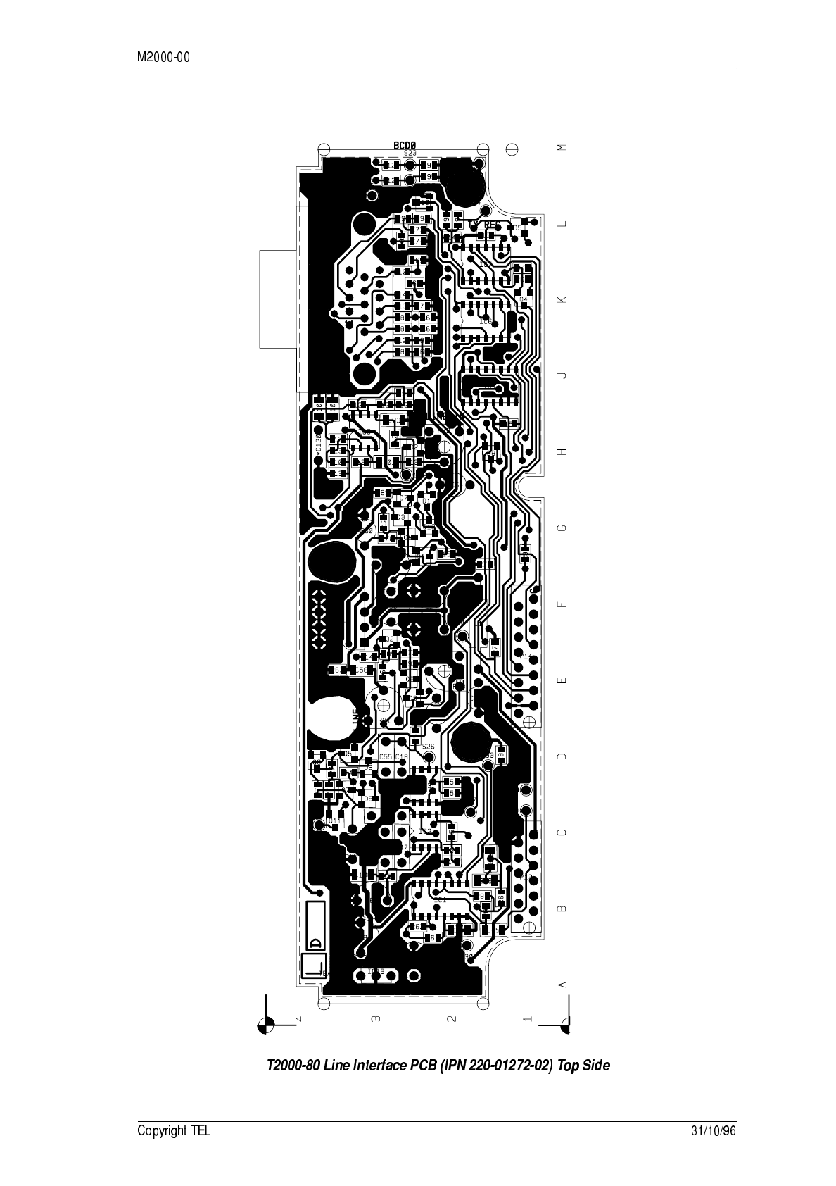
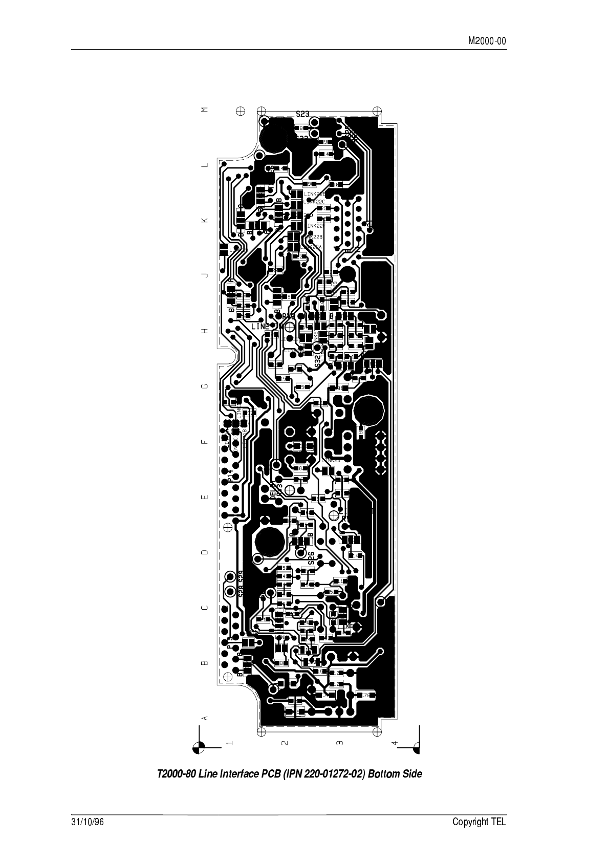
The T2000-80 line interface kit enables connection of the T2000 receiver and transmitter
audio circuitry to a two wire transmission line. The line interface PCB is mounted in the
options position inside the T2000 Series II radio, and is application configurable using
PCB links.
The following topics are covered in this Section:
Section Title Page
8.14.1 Components Required 8.14.2
8.14.2 Fitting 8.14.2
8.14.3 Line Interface Options 8.14.4
8.14.4 T2000-80 Set-Up 8.14.7
8.14.5 Signal Specifications 8.14.9
8.14.6 Applications 8.14.10
8.14.7 Specifications 8.14.16
8.14.8 Circuit Description 8.14.18
8.14.9 PCB Information 8.14.21
673)
!)6(
The T2000-80 kit contains the following components:
.
&
1Refer to Figure 8.14.1.
Remove the top cover of the radio by unscrewing the four cover screws, unclip the
D-range blanking plate in the rear of the T2000 radio, unscrew the logic PCB and
fold-out.
Position the T2000-80 PCB as shown, and connect the Micromatch connectors P13
and P14 to S13 and S14 on the T2000 logic PCB.
2 T2010 & T2015: Remove R513 (0Ω resistor) on the logic PCB.
Quantity Description
1 T2000-80 Line Interface PCB assembly
1 15-way high density D-range plug
1 shroud (alternative shroud - not required for T2000 Series II radios)
28 0Ωchip resistors
1 1µ capacitor (*C64)
1 4µ7 capacitor (*C60)
3 M3x8 pan Pozi Taptite screws
2 4-40x¼ pan Pozi Taptite screws (black)
T2000-80 PCB
S24
S21
CGND
BCD1
BCD0
TP609
T2010 & T2015
Logic PCB
S1
S2
S13
P13 P14
S14 S15
SK505
P2
P1

673)
3 Tx/Rx Out Function
Connect a wire from S24 on the T2000-80 PCB to S609 on the logic PCB, as shown
in Figure 8.14.1.
4 External Channel Control (T2010 Only)
Connect the 2 BCD lines a shown in Figure 8.14.1.
5Refer to Section 8.14.3, “Line Interface Options”, Section 8.14.6, “Applications”
and the circuit diagram before selecting the T2000-80 PCB linking options.
Set up the T2000-80, as described in Section 8.14.4, “T2000-80 Set-Up”.
6Carefully fold the logic and T2000-80 PCBs back in position, guiding the D-range
connector through the hole provided in the T2000 chassis.
Secure using the three logic PCB retaining screws and the three M3x8 screws pro-
vided, and refit the top cover.
Plug the D-range assembly provided in the kit into the D-range connector (S21).
Holes are provided in the T2000 chassis for the D-range plug locking screws.
Use the two black 4-40 Taptite screws provided in the kit to form the threads.
673)
#
;#8
Provision has been made on the T2000-80 PCB for many different application condi-
tions. Refer to the circuit diagram, PCB layout, the T2000 options connections table
below, and the T2000-80 Signal Specifications table for details of options and links.
The PCB links are either solder shorted or fitted with 0Ω SMD resistors.
To prevent the possibility of damage, check the Signal Specifications table
before attempting to change the configuration.
The following table sets out the standard T2000-80 linking options for T2010 and T2020
models.
((!
*C60 (4µ7):This is provided to give a slight time delay to the Rx gate signal, if required.
*C64 (1µ): This is provided to give a slight time delay to the release of transmit, if
required.
*C120 (4n7): Provision has been made on the PCB to fit an extra potted mylar capacitor
for line matching, if required.
Link Option
LINK1A Rx de-emphasis
LINK2B
LINK27B
LINK28B
6 pole line output filter
LINK3A
LINK4A 600 ohm output
LINK5 0dB line output attenuation
LINK9 Line input and output linked
LINK12B
LINK13 Tx pre-emphasis
LINK16A Mic. mute on line input PTT
LINK17A Rx gate standard radio (T2010/T2020)
LINK18A Opto control standard
LINK19A Auxiliary control
LINK20A PTT in
LINK21A Key (0V)
LINK22B Busy (0V)
LINK24A Output (Tx5V/Rx0V)
LINK26B Synth in Lock (0V)
673)
;(!
The following table describes the T2000-80 pad connections found on the bottom side of
the T2000-80 PCB.
Pad Signal Description
S22 BCD1 Connect to S15 pins 9 (BCD0) and 10 (BCD1) on T2010 logic PCB for
channel remote switching. Enabled in software.
S23 BCD0
S24 TX-REG Output indicating whether the radio is transmitting or receiving.
Used for modem control applications.
Tx = +5V
Rx = 0V
S25 Spare Uncommitted line to S21
S35 CGND True ground used for RF decoupling capacitors. Must be connected
to radio chassis if logic and T2000-80 PCBs are folded out during
set-up and test.
* 673)
!
The following table described the signals used for line interface on P13 and P14.
Pin
No. Signal Description
P13-1 DET-AF-OUT Output, buffered and low pass filtered, for flat response (60% devia-
tion, 0.25Vp-p, 1kHz).
P13-3 RX-LINE-OUT De-emphasised and high pass filtered output (60% deviation,
0.4Vp-p, 1kHz). High pass filter circuit depends on presence of
sub-audible tone signalling. Used for de-emphasised response.
P13-6 TX-LINE-IN Input to pre-emphasis stage, bypasses compressor. Used for the
pre-emphasised response (60% deviation, 0.3Vp-p, 1kHz). Line
input will override microphone signal if both are present.
P13-8 TX-SIG-IN Low gain input to T2000 limiter stage. Bypasses pre-emphasis and
high pass filtering, used for the flat response (60% deviation,
2.2Vp-p, 1kHz).
P13-11 OPT-GND Earth from the regulator section of the T2000 main PCB. Used to
avoid earth loop noise.
P13-12 +13.8V-UNSW Unswitched +13.8V supply from the T2000. Powers audio PA and
external opto key circuits.
P14-1 +13.8V Switched +13.8V supply from T2000. Powers line interface PCB +8V
regulator.
P14-2 +5.0V +5V from T2000 main PCB regulator. Powers hex invertor ICs and
trunking switches.
P14-3 BUSY Output BUSY = 0V is used to inhibit line input derived key and line
input mutes. On trunked versions is used for inhibit logic.
P14-4 RX-GATE Output port used to open the mute element in the T2000. Used to
control line output mute.
Note: Unmute = +5V for T2010 and T2020;
Unmute = 0V for T2030 and T2040.
This also drives the line key and opto driver indirectly.
P14-5 PTT-TO-OPT Output mirrors PTT from microphone or signalling. PTT = 0V. On
trunked versions is used for inhibit logic.
P14-6 PTT-FROM-OPT Input port to key transmitter. Used for line input derived key and
microphone derived key.
P14-7 IN-LOCK Synthesiser phase lock detector output. Used for modem control
applications. Lock = 0V.
P14-8 MIC-MUTE Input port used to disable local microphone signal on line input
derived PTT (not on microphone PTT). Mute = +5V.
P14-13 AUX Auxiliary control output configurable in software. Used to enable/
disable crossband linking, 2 wire linking etc. (see trunked versions).
Aux on = +5V.
Trunking Models: Additional Functions
P14-5 PTT-TP-OPT For inhibiting modem output on PTT from microphone.
P14-10 EMERG Performs a new function. ‘External call request’ = 0V input. Used
for modem calls on a trunked system.
P14-11 CALL-SW Performs a new function. ‘Traffic channel allocated’ = +5V output.
Used for modem calls on trunked system.
P14-13 FCN/BELL/AUX Performs a new function. ‘Not clear to send’ = +5V output. Used for
modem calls on trunked system.
673) +
;;4
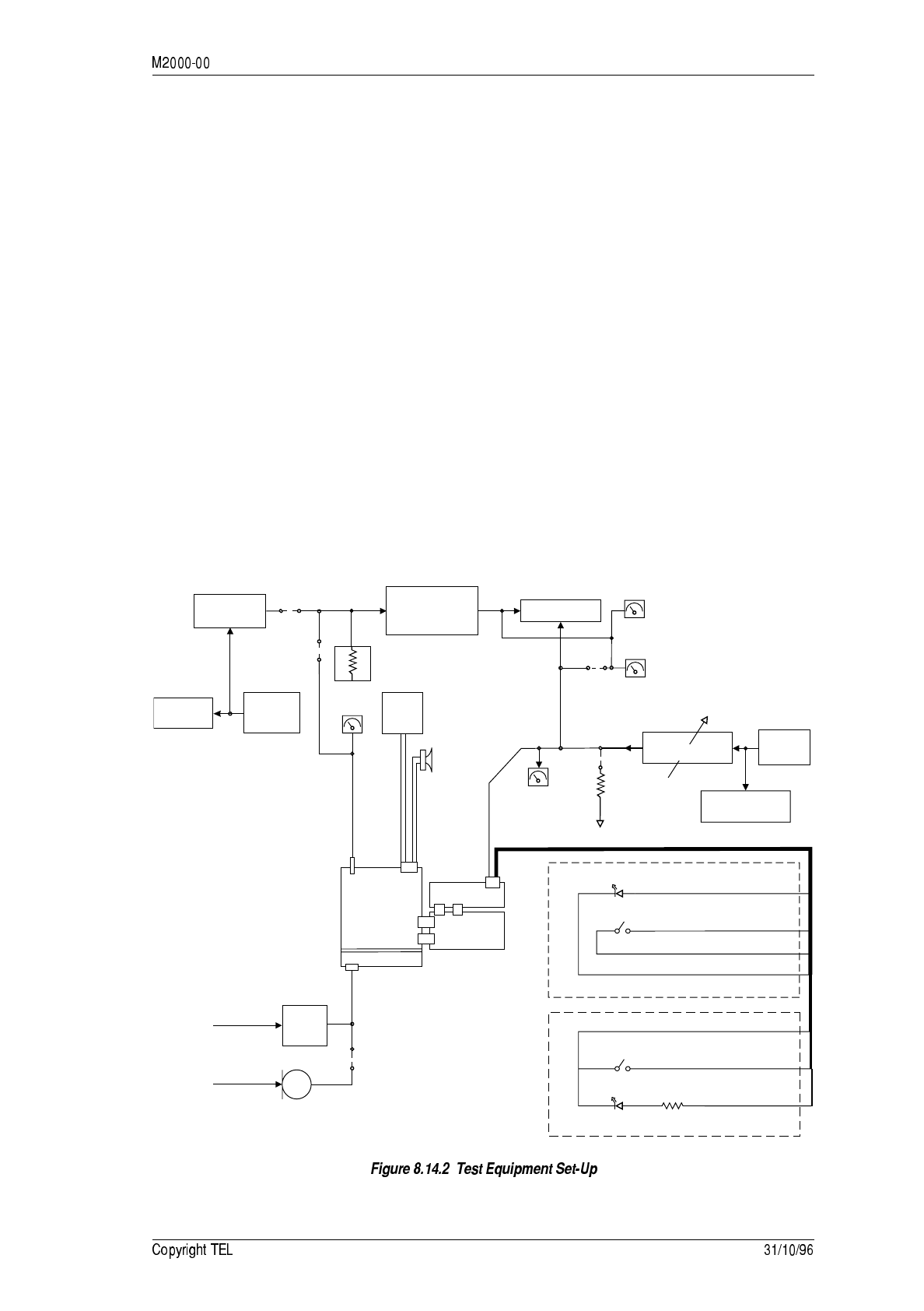
56)6(
• AF signal generator
• distortion analyser
• frequency counter
• Modulation analyser
• High impedance voltmeter (e.g. VTVM)
• Oscilloscope
• Power meter
• Power supply (+13.8V)
• RF signal generator
• 40dB RF attenuator
• 600Ω step attenuator
The following diagram shows the test set-up.
RF RF
4Ω
Speaker
Line In/Out
600Ω
Pwr/Spkr
Option Board
Control Board
RF
OPT
S21-12
Busy/Rx Gate Out
1K
5V Logic
S20-10 Gnd
DC Control
S21-1 Opto In
Opto In
S21-4 +13.8V Out
S21-3 +8V Out
Opto Key
S21-2 Opto Out
Frequency
Counter
AF
Signal
Generator
Ext. AF
RF Signal
Generator RF Modulation
Analyser AF
+13.8V
Power
Supply
40dB
Pad
Power
Meter
Dummy
Mic. &
PTT
Audio
Voltmeter
Audio
Voltmeter
Distortion
Meter
AF
Signal
Generator
Oscilloscope
Frequency
Counter
T2000
Main
Board
Test Signal
600Ω
Step Attenuator
Mic. Socket
Test Signal
(Speech) Test
Mic. &
PTT
S20-11 PTT In
673)
;4
1The adjustment section assumes that the T2000 radio has been correctly aligned
for normal operation. Refer to Section 8.14.3, “Line Interface Options” and the cir-
cuit diagram for linking and application details.
2If the logic and T2000-80 PCBs are unscrewed and folded out for adjustment, a
wire should be temporarily fitted from the radio chassis to the options chassis
ground pad (S35), as shown in Figure 8.14.1.
3Signals for balanced transmissions are generally less than 0dBm, and are typically
between -10dBm and -20dBm.
4Ensure that the LED is on ( LED on trunking radios).
Deviation settings are given first for wide band radios, followed by settings for
narrow band radios in brackets [ ].
##,
1Ensure that the LED is on ( LED on trunked radios).
2Monitor the line output (S21 pin 5).
Apply an on channel signal from the RF signal generator at an output level of
-70dBm, modulated to ±3kHz [±1.5kHz] deviation, at 1kHz AF.
Adjust the RV1 (line output control) for the required output level.
If the line output level is to be less than -15dBm, short LINK6 (600Ω output) and
remove LINK5, to select 15dB of attenuation.
#,
1Monitor the line input (S21 pin 15).
Ensure the indicator is off, and key the transmitter via the opto input (+8V).
2Adjust RV2 (line input sensitivity control) until ±3kHz [±1.5kHz] deviation at
1kHz is achieved.
For input signals of greater than -15dBm, set the line input attenuation for 15dB
(LINK11 open).
7
!
This circuit delays audio gate turn on after PTT, to prevent squelch noise bursts in
repeater applications.
1Enable the time delay circuit by solder shorting LINK23.
2Set the required time delay using RV3 (time delay control).
Fn
Fn
673) -
&
The following table describes the electrical specification of T2000-80 interface signals
available at the 15 way high density D-type connector (S21), mounted on the heatsink at
the rear of the radio.
The following diagram shows the pin designations of S21, viewed from the rear of the
radio.
S21
Pin No. Signal Description
1 OPTO-IN Input for external opto coupled line current detector.
+8V logic.
2 OPTO-OUT Output to drive external opto coupled line current switch.
1k ohm series resistor for LED.
3 +8V-OUT +8V output to supply external opto coupled line current detector.
4 +13.8V-OUT Unswitched +13.8V output to provide an unisolated keying sup-
ply.
5 LINE-OUT Output audio path to transmission line or transformer.
6 KEYING Bi-directional key line for use with simple two wire linking
(optionally linked to OPTO-IN internally). +8V logic.
7 BCD0-OUT Inputs used for 4 channel remote switching
with the T2010. +5V logic.
8BCD1-OUT
9 Spare Decoupled uncommitted line.
10 GND Options ground. This is earth derived from the regulator section
of the T2000 main PCB. Used to avoid earth loop noise.
11 PTT-IN Keys transmitter and operates line control logic. Trunking PTT
selectable. +5V logic, sense selectable by links.
12 BUSY/GATE Busy or Rx gate output. Trunking busy link selectable. +5V logic,
sense selectable by links.
13 IN-LOCK-OUT Synthesiser lock detector output. +5V logic, sense selectable by
links.
14 TX/RX-OUT Tx regulator control output. Indicates whether the radio is in Tx
or Rx. +5V logic, sense selectable by links.
15 LINE-IN Input audio path to transmitter audio stages. Normally linked to
LINE-OUT for a bi-directional line but is able to be separated for
other applications using two transmission lines.
- CGND Provided via S21 D-range and cable screen if required for RF sus-
ceptibility.
51
10 6
1115
PCB

673)
*
.
The frequency response of the line output low pass filter is selectable by LINK2, LINK27
and LINK28.
• 2 pole: -12dB/octave stopband attenuation, f > 4kHz.
• 6 pole: -36dB/octave stopband attenuation, f > 4kHz.
The 2 pole LPF is for applications requiring minimal group delay and stopband attenua-
tion, e.g. standard configuration, crossband 2 wire + earth, modem connection.
The 6 pole LPF is for applications requiring external network connection where stop-
band attenuation is mandatory above 4kHz, e.g. crossband via external network (bal-
anced line + opto key), remote controlled audio via external network (balanced line +
opto key).
673)
9#8
&
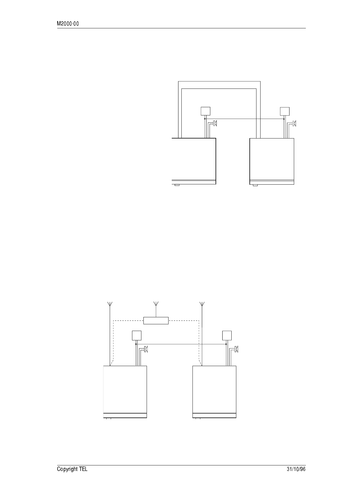
This is the control of 2 radios operated together, crossband or repeater linked.
1Check that LINE-OUT is linked to
LINE-IN internally (LINK9 fitted).
Fit LINK15 to link KEYING to
OPTO-IN. This provides control in
both directions. The unit generat-
ing the keying signal is already Tx
inhibited.
2Wire LINE-OUT (S21-5) on one
T2000 to LINE-OUT (S21-5) on the
other T2000. Wire KEYING (S21-6)
on one T2000 to KEYING (S21-6)
on the other T2000.
T2000
No. 1
-+
Power Suppply
13.8V
4Ω
Speaker
Pwr/Spr
T2000
No. 2
-+
Power
Suppply
13.8V
4Ω
Speaker
Pwr/Spr
HD
D-Range
HD
D-Range
Line Out to Line Out
Keying I/O to Keying I/O
3The time delay circuit may be required to eliminate squelch noise bursts for cross-
band operation with repeaters. LINK23 enables this circuit, which is adjustable
using RV3 (refer to Section 8.14.4, “T2000-80 Set-Up”).
The 2 wire circuit assumes that the 2 radios are effectively earthed together at
either the power supply or the power connector.
A high line level is desirable to avoid earth noise i.e. 0dBm (0.775Vrms).
!3()(
Crossbanded radios i.e. UHF/VHF, can be achieved by using space isolated antennas to
avoid de-sensing, as shown below.
Alternatively, in-band linked radios will require a duplexor to feed a common aerial.
T2000
No. 1 T2000
No. 2
-+-+
Power Suppply
13.8V Power Suppply
13.8V
4Ω
Speaker 4Ω
Speaker
Pwr/Spr Pwr/Spr
Duplexor
Common Antenna UHF AntennaVHF Antenna
RF RF
673)
5=!.#?
&
</(!
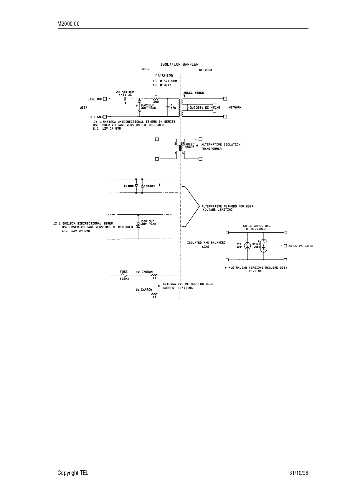
The T4030, 4N38A and 4N25A are not intended for mains rated isolation.
• Mains rated transformer: Arlec 45035 (suitable for PSTN lines) 600/600 only, 4kVrms
rated.
• HV rated transformer: Arlec 45065 (suitable for private lines) 600/600 or 600/150,
3.5kV rated.
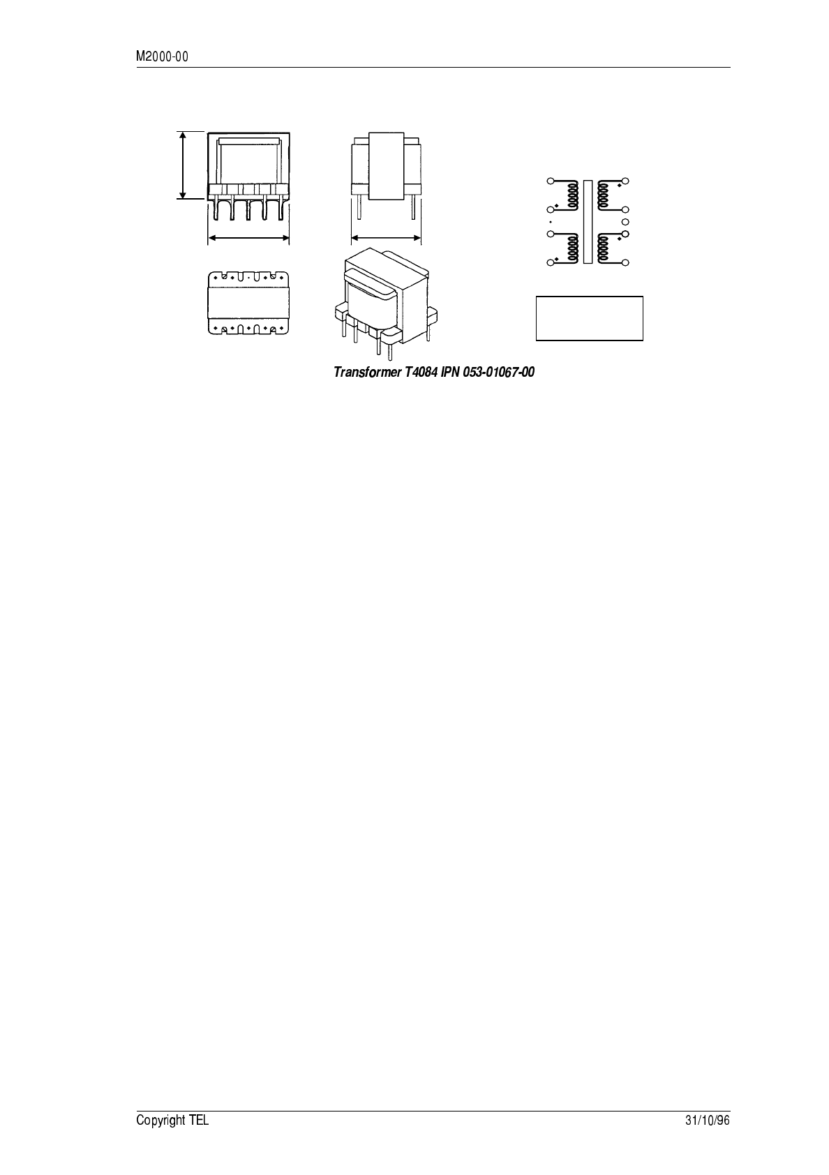
• Transformer T4084: 2kVrms.
• Transformer T4030: no HV specification.
• Mains rated opto-isolators: CNY17G
CNW85
Refer to the M008-50 Service Manual for line keying connection diagrams.
673)
#/A,#
Refer to Austel Technical Standard TS 001:1991 ‘Safety Requirements For Customer
Equipment’ for other configurations.
These circuits will require approval to the appropriate standards before use.
• Mains isolation: 4kVrms/8mm CrCl required + 2.5mm CrCl from protective earth on
surge arresters.
• Private lines: 3.5kV.
• Arlec 45035: PSTN/mains rated.
• Arlec 45065: private line rated.
673)
"
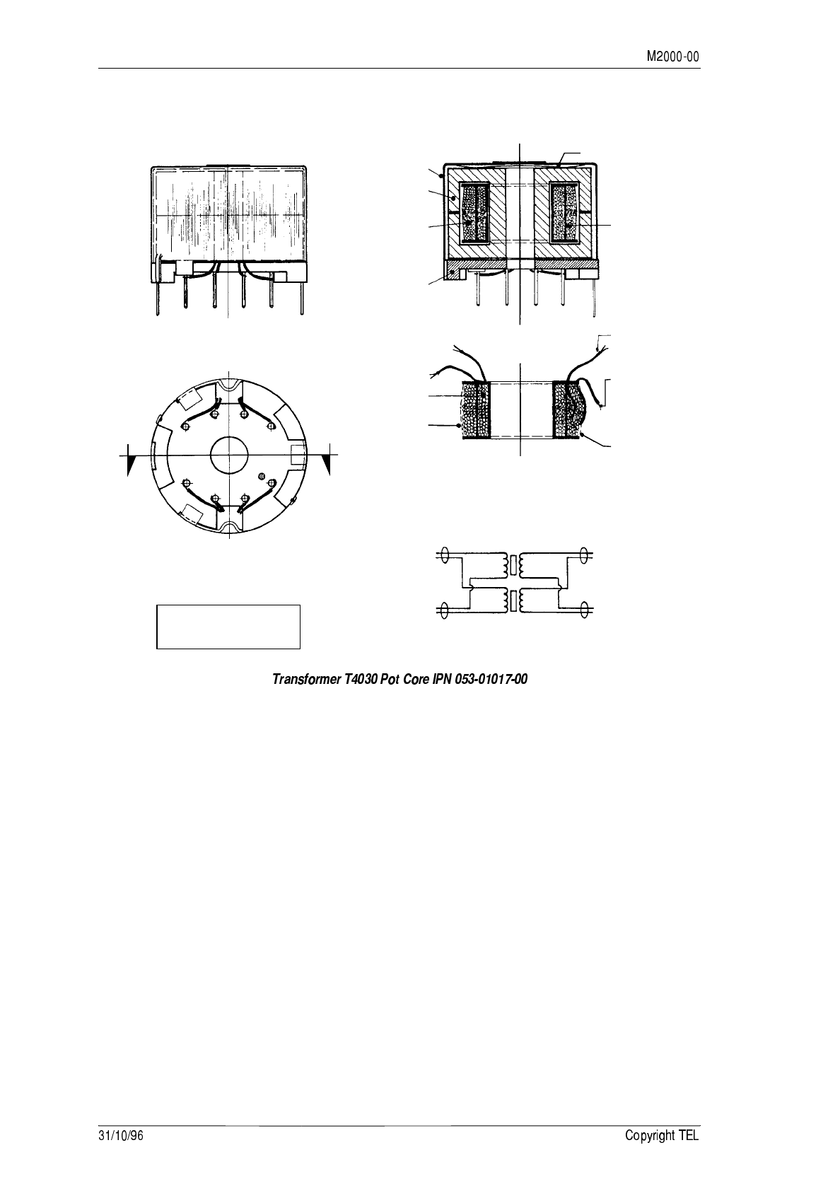
Cores must be properly aligned when assembled.
Core faces must be clean and free from grease and dirt.
Ensure tag plate is firmly pressed against can before folding tabs.
Core .. P26/16 - µ1910
Former .. single
Number of Turns:
Primary .. 250 bifilar
Secondary .. 250 bifilar
Material .. 15mm self flux
Tape .. thermosetting electrical grade
Sleeving .. inside diameter all colours, 0.5mm
Inductance 1 .. 6±1.5H
(total series inductance, pin 1 to 5 - connect pins 2 & 3, 4 & 8 and 7 & 6)
Inductance 2 .. 1.5±0.4H
(any winding, with all others open circuit)
Secondary
Primary
5678
432
1
Underside View
Can
Core
Former
(Wound)
Tag plate
Spring
Mylar
Insulator
Section A-A
Primary
Secondary
Leads to
be sleeved
Tin ends
of leads
Tape outside
of turns
Former and Windings
1
3
2
4
Sleeving
Colours Sleeving
Colours
Start
Pri
Bifilar
Finish Finish
Pri 250T - 15 Red & Green
Sec 250T - 15Red & Green
Green
250T
Green
250T Red
250T
Red
250T
8
6
7
5
Brown
Blue
Red
A
A
Start
Sec
Bifilar
Grey
Sleeving Colours:
Pin 1,3 Brown 2,4 Red
5,7 Blue 6,8 Grey
673)
"
Impedance .. 600Ω /600Ω centre tapped, separated
Output Level .. 0dBm at 1kHz
Frequency Response .. +0.2dB, -0.5dB 300Hz to 3400Hz
relative to 1kHz at 0dBm output
Insertion Loss .. <0.75dB, 0dBm output at 1kHz
Return Loss (relative to 600Ω):
At 1kHz .. >15dB
At 300Hz .. >10dB
Distortion (unbalanced currrent):
1kHz 0dBm out 0mA DC .. <0.2%
1kHz 0dBm out 5mA DC .. <0.7%
300Hz 0dBm out 0mA DC .. <1.0%
300Hz 0dBm out 5mA DC .. <6.0%
Level reduction due to 5mA DC at 300Hz .. <2dB
Impedance Balance About Earth .. >46dB over 50Hz to 3400Hz
Insulation:
DC Primary to Secondary .. 500V R>10MΩ
Primary & Secondary to core .. 500V R>I0MΩ
A.C.Primary to Secondary .. 2kVrms 60sec.
Primary & Secondary to core .. 2kVrms 60sec.
Ferrite Core .. see 16 x 7 10 Pin Bobbin Harvard Inds.
Ref. Cerf. 2611
Primary Inductance .. 500mH ±50mH typical
(1kHz 1 to 5, 2 & 4 connected together)
Leakage Inductance .. 700µH ±100µH typical
(10kHz; 1 to 5, 2 & 4 connected together, 6, 7, 9, & 10 connected together)
Primary DC Resistance:
1-2 .. 8.3Ω typical
4-5 .. 8.3Ω typical
Secondary DC Resistance:
10-9 .. 14.6Ω typical
7-6 .. 14.6Ω typical
600ΩSecondary
10 to 6, 9 & 7
connected together
600ΩPrimary
1 to 5, 2 & 4
connected together
6
7
8
9
10
5
4
3
2
1
All Dimensions in mm.
Scale: 2:1 (Approx.)
Material: See Notes
General limits: 0.2
15
16.5 14.2
678910
Pin 1 2 345

* 673)
+
;
Input Voltage .. 10.8V to 16V DC
(from S13 & S14 on the T2000 logic PCB)
Operating Temperature Range .. -10°C to +60°C ambient
DC Input Current .. < 40mA total (+13.8V supply)
Line Input Sensitivity (60% deviation) .. -20dBm to +6dBm (600Ω)
Line Output Level (60% deviation) .. -20dBm to +6dBm (600Ω)
Line Impedance .. 600 or 150Ω
Return Loss (300Hz to 3kHz). .. > 20dB relative to 600 or 150Ω
Line Output Filter Response (stopband):
2 pole .. -12dB/octave, f > 4kHz
6 pole .. -36dB/octave, f > 4kHz
B;#
a Receiver + Line Output
Receiver Frequency Response (relative to 1kHz, 60% deviation):
Receiver Processed:
Bandwidth .. 300Hz to 3kHz (standard)
400Hz to 3kHz (CTCSS)
Response .. +1, -3dB relative to -6dB/octave
Receiver Unprocessed .. +1, -3dB (300Hz to 3kHz)
Test signal .. -70dBm RF, 60% deviation at 1kHz,
0dBm line output.
Signal-to-Noise Ratio:
Narrow Band .. > 39dB
Wide Band .. > 45dB
Mute Ratio .. > 65dB
Distortion (30kHz band width distortion meter):
Wide Band De-emphasised .. < 2%
Narrow Band De-emphasised .. < 3%
Wide Band Flat .. < 4%
Narrow Band Flat .. < 6%

673) +
b Transmitter + Line Input
Transmitter Frequency response:
Transmitter Processed:
(relative to 1kHz, 20% deviation, below limiting)
Bandwidth .. 300Hz to 2.55kHz (narrow band)
300Hz to 3kHz (wide band)
Response .. +1, -3dB relative to +6dB/octave
Transmitter Unprocessed (relative to 1kHz, 60% deviation):
Bandwidth .. 300Hz to 2.55kHz (narrow band)
300Hz to 3kHz (wide band)
Response .. +1, -3dB
Test signal .. 0dBm line input, 1kHz, 60% deviation
Signal-to-Noise Ratio:
(demodulated, filtered 300Hz to 3kHz + de-emphasised 750µsrms)
Narrow Band .. > 39dB
Wide Band .. > 45dB
Distortion .. < 2%
(demodulated, filtered 15kHz low pass)
673)
!7
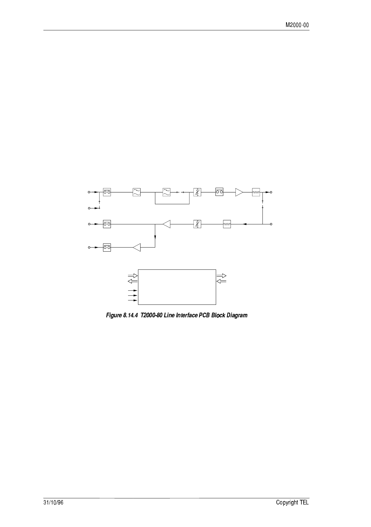
Refer to Figure 8.14.4, Figure 8.14.4 and the circuit diagram.
#$
Flat or de-emphasised audio from the receiver is selected by links to DET-AF-OUT or
RX- LINE-OUT. Receiver audio passes through a mute element to a buffer amplifier, and
then to three stages of low pass filtering. Two responses are selectable by links: 2 pole or
6 pole roll-off beyond 4kHz.
The filtered signal passes to a second mute element and level control before passing to
the line output drive amplifier. Line output impedance and attenuation are selectable by
links. Line output can be linked to line input for a shared line in, line out.
#$
The line input has terminations for two line impedances which are link selectable. The
line input level can be attenuated, if required, before passing to the line sensitivity con-
trol. Protection diodes are fitted to prevent the following amplifier stage from being
overdriven.
The amplifier provides gain and buffers the signal, which is split into two paths for
either pre-emphasis or flat response. The pre-emphasis path is via a mute element and
options linking. This signal drives TX-LINE-IN, which will override the microphone
signal. Normally, the microphone is muted on line derived PTT.
The flat response path is amplified and then passes to a mute element which drives
TX-SIG-IN. This input requires a high signal level, due to the high input impedance.
The amplifier is disabled by links, when not used, to prevent the possibility of crosstalk
and leakage to other circuitry.
Control Logic
External
Logic
T2000
Logic
Power
Suppliers
Line
Driver
Attenuator
Attenuator
Mute
Element
Mute
Element
Mute
Element
Mute
Element
Line Out
Level
Link2
BA
N=4N=2
Gain
Stage
Buffer
Amp Line
Sensitivity
Line Out
Line In
T2000
Control PCB
Via Option
Connectors
RxAF
De-Emph.
RxAF
Flat
TxAF
Pre-Emph.
TxAF
Flat
External Circuits
Via HD D-Range
Connector
673) -
!#&
For standard mobiles in normal operation, the audio mute elements, transmit inhibit
and opto driver are all inhibited by the auxiliary control. The radio can be used nor-
mally with ‘auxiliary off’, and line controlled with ‘auxiliary on’.
With ‘auxiliary on’, the line output mute elements and opto driver are controlled from
the RX-GATE. A signal on the BUSY line inhibits the transmitter line key circuitry. Line
derived key signals, such as OPTO-IN, KEYING and PTT-IN, can be used to key the
radio, provided the auxiliary control is on and the radio is not busy.
The KEYING line is used for back-to-back control of two radios, each with a line inter-
face PCB. This enables crossband linking to be achieved with a minimum of external cir-
cuitry. In this case, the KEYING line can be linked to the OPTO-IN line on each unit,
with a wire between the two OPTO-IN lines providing bi-directional control. KEYING is
controlled by the receive gate and is used to drive the opto input of another line inter-
face PCB.
The opto input is intended to be connected to the output of an optocoupler circuit (BJT)
used for loop and tail keying via transmission lines (refer to Section 8.14.6, “Applica-
tions”).
The opto output is intended to be connected to the input of an optocoupler circuit (LED)
used for loop and tail keying via transmission lines (refer to Section 8.14.6, “Applica-
tions”). The sense of this circuit can be changed by a link.
An adjustable time delay circuit is available to prevent transmitter cycling when cross-
band connected radios are both operating on repeater channels. The circuit is adjustable
to approximately 1.5 seconds, with the time delay control fully clockwise, and can be
disabled completely by removing a link.
PTT-IN can be used to key the transmitter. Links are available to enable either logic
sense. For trunked versions using modems, a circuit is provided to set up a call automat-
ically.
Control logic for telemetry and modems is provided so that the radio can be operated
automatically. IN-LOCK-OUT, BUSY/GATE and TX/RX-OUT outputs can be set by
links for either logic sense.
Trunked modems operate in a different manner, and first have to set up a call to obtain a
traffic channel allocation.
Logic is available which requires several link changes, as some of the radio options con-
nections perform different functions:
Standard Trunked
AUX on/off not clear to send
emergency external call request
call traffic channel allocated

673)
+5V is provided from the main regulator via the options connector. +8V is provided by a
TO-92 3 terminal regulator. This is also available on the T2000-80 PCB D-range connec-
tor, for powering an optocoupler transistor used for line key current detection. The
+13.8V input of the regulator is derived from the options connector. The +3.2V rail pro-
vides bias to the audio stages and is derived from the +8V regulator. The unswitched
+13.8V from the options connector powers the line drive amplifier, and is available on
the T2000-80 D-range for use as an unisolated line key supply option.
;#0:;+;2
673)
- !/
673)
'$<'
673)
;()(=0:;+;2
673)
Notes: 1/ Remove R77 for trunked modem operation
or, in non-trunked radios, to remove external
inhibit on busy.
2/ R90, R91 should be removed for two-wire
crossband when moulded cord sets are used. (HD15M-HD15M)
This is to avoid PSU conflicts between radios.
(+8V out, +13V out.)
;%<30:;+;2
673)
* 673)
#*2')
;+7'(?
The T2000-A70 conventional data modem allows a T2010 or T2015 radio to be used in
data applications, and also provides remote channel control via six BCD lines.
The command protocol and some test procedures are provided for those wanting to
write their own software. The protocol definition is based on the T2000 CCI protocol,
with specific extensions to support binary transmission and reception.
This interface is only compatible with radio firmware version 2.22, or later. If
you have a Series II HC05 logic PCB (PCB IPN 220-01377-0X), with v2.05 radio
firmware, contact your nearest authorised Tait dealer.
After upgrading from v2.05 radio software, it is necessary to change the link
resistors on the top side of the logic PCB. Remove link resistor #R714 and fit
#R714A.
The following topics are covered in this Section:
Section Title Page
8.15.1 Components Required 8.15.2
8.15.2 Fitting 8.15.2
8.15.3 T2000-A70 Link Options 8.15.4
8.15.4 Signal Specifications 8.15.5
8.15.5 Programming 8.15.6
8.15.6 Circuit Description 8.15.12
8.15.7 PCB Information 8.15.13
#*2')
!)6(
The T2000-A70 kit contains the following components:
.
&
Refer to Figure 8.15.2.
1Remove the top cover of the radio by unscrewing the 4 bottom cover screws,
unscrew the logic PCB and fold out.
2 T2000-A70 Mounting
Position the data modem PCB on the top side of the logic PCB, as shown, match-
ing P3 on the bottom side of the data modem PCB to connector S3 on the logic
PCB.
Use the 2 M2.5x10mm screws, nuts and shakeproof washers to secure in place, as
shown.
The screws are fitted from the bottom of the logic PCB, and secured with the nuts
and washers on the top side of the data modem PCB.
Torque the screws to 2.5in.lb.
Over-tightening the screws will cause damage to the data modem PCB,
and compression of connector P3.
* Discard unused parts from the female screw lock kit.
Quantity Description
1 T2000-A70 data modem PCB assembly
1 Data interface decoupling PCB assembly (refer to Section 7.17)
1 connecting loom
2 M2.5x10mm pan Pozi Taptite screws
2 M2.5 shakeproof washer
2 M2.5 nut
1 female screw lock kit (in plastic bag)*
24-40x
5/16 pan Pozi Taptite screws (black)
#*2')
3 T2000 Data Interface Decoupling PCB Mounting
Unclip the D-range blanking plate in the rear of the T2000 chassis.
a T2000 Series I Chassis
Refer to Figure 8.15.3.
Holes are provided in the T2000 chassis for the D-range screw locks. Use the 2
black 4-40 Taptite screws provided in the kit to form threads.
Fit the decoupling PCB to the T2000 chassis, guiding the PCB through the hole
provided, as shown.
Open the female screw lock kit, then secure the D-range using the 2 screw locks
and spring washers.
#*2')
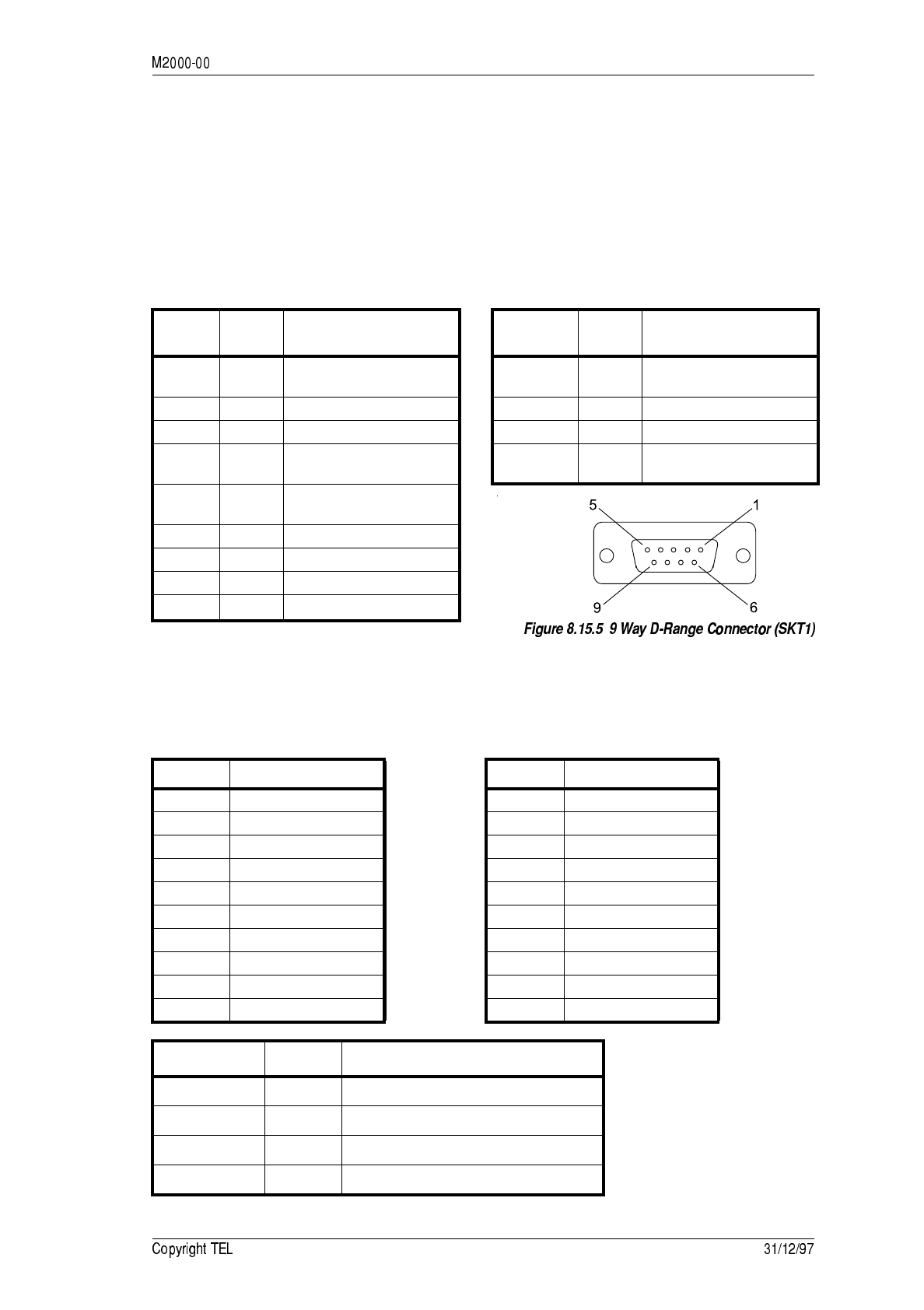
b T2000 Series II Chassis
Refer to Figure 8.15.4.
Fit the decoupling PCB to the T2000 chassis, from the inside rear of the radio, as
shown.
Secure the D-range in position using the screw locks, spring washers and nuts
provided in the female screw lock kit.
4Fold the data modem loom as shown, then plug into SKT2 on the decoupling PCB.
5Fold the logic PCB back in position, secure using the 3 logic PCB retaining screws,
and refit the top cover.
Check that the loom is not pinched by the cover or screws during reassembly.
;+#8
PCB links have been provided on the T2000-A70 data modem PCB for different opera-
tional requirements. To change settings, the PCB links are either solder shorted, or fitted
with 0Ω SMD resistors.
The following table sets out the link selection options on the T2000-A70 data modem PCB.
Option #R19 #R2010 #R2015
Baud Rate:
1200 Fitted - -
2400 Not fitted - -
Radio Type:
T2010 - Fitted Not fitted
T2015 - Not fitted Fitted
#*2')
&
77&!/
The following tables describe the signals on the decoupling PCB 9 way D-range connec-
tor (SKT1) and 4 way connector (SKT2). The diagram shows the pin designations of
SKT1, viewed from the rear of the radio.
Pins 1, 4, 6, 7, 8 and 9 on SKT1 are connected to I/O pads, so that additional sig-
nals can be interfaced to the radio through the external connector.
7'(!/
The following tables describe the signals on the data modem PCB connectors P3 and
PDL-1. For P3 signal descriptions, refer to Section 5.9, “Options Interface Specifica-
tions”.
SKT1
Pin No. Signal Description SKT2
Pin No. Signal Description
1 PAD1 Spare 1 DGND Ground reference for all
digital signals
2 TXD Transmit data 2 RXD Receive data
3 RXD Receive data 3 TXD Transmit data
4 PAD2 Spare 4 DGND Ground reference for all
digital signals
5 DGND Ground reference for all
digital signals
6PAD3Spare
7 RTS Spare
8 CTS Spare
9PAD4Spare
P3 Pin No. Signal P3 Pin No. Signal
1 BCD-0 11 /PTT-TO-OPT
2BCD-1 12/RX-GATE
3BCD-2 13/IN-LOCK
4 BCD-3 14 /PTT-FRM-OPT
5 BCD-4 15 /SIG-SQUELCH
6 BCD-5 16 MIC-MUTE
7 TX-SIG-IN 17 DGND
8 DET-AF-OUT 18 PWR-CTRL
9/BUSY 19GND
10 N/C 20 +5V
PDL-1 Pin No. Signal Description
1 DGND Ground reference for all digital signals
2 TXD Transmit data
3RXDReceive data
4 DGND Ground reference for all digital signals
* #*2')
&
&
For those wanting to write their own software, the command protocol and some test
procedures are provided in this Section. The protocol definition is based on the T2000
CCI protocol, with specific extensions to support binary transmission and reception.
For modem control of channel change, the BCD Channel Selection field in the
Edit - Options menu must be set to Enabled during radio programming.
!33,
CCI Computer Controlled Interface
DTE Data Terminal Equipment (e.g. Computer, data head)
RU Radio Unit
RXD Received Data
TXD Transmitted Data
!(7
The DTE is connected to the RU via a serial port on the data modem PCB. Commands
are generated by the DTE, and responses or unsolicited messages returned by the RU.
There is a prescribed format for all messages, which allows transmission errors to be
detected.
Control of the RU is accomplished by the DTE sending a command sequence (a
“packet”) and receiving a response (a “transaction”). Unsolicited messages may origi-
nate from the RU.
The RU will issue a prompt character to indicate to the DTE that it is ready to accept a
new command. After issuing a command, the DTE must wait for another prompt before
beginning the next transaction. The prompt character is “•” (full stop, ASCII code =
$2E).
Messages directed to the RU will always be responded to, either explicitly by means of a
return message (“Ready” or “Error”), or implicitly, by just the prompt “•” being issued.
The RU will not originate a message: messages returned by the RU are for information
purposes only, and no reply will be expected from the DTE.
This protocol definition is based on the T2000 CCI protocol, with specific extensions to
support binary data transmission and reception.

#*2') +
'&.
All message packets take the general form:
[IDENT][SIZE][PARAMETERS][CHECKSUM]<CR>
The following table explains each component of the message packet.
General message format characteristics:
• All fields in a message are encoded in ASCII, except for the [PARAMETERS] field of
the transmit and receive commands, which is encoded in Binary.
• Where numeric values are represented in ASCII-hex notation (two characters per
byte), digits A to F are upper case.
• The minimum length of a command packet is 5 characters (i.e. this is when [SIZE] =
00).
• The maximum length of the [PARAMETERS] field is 111 characters. The maximum
length of the command packet is therefore 116 characters ([SIZE] = 0x6F).
Message Component Description
[IDENT] The message identifier. Identifiers are single ASCII characters (lower-case
alphabetical) which categorise the message type.
[SIZE] The number of characters which make up the [PARAMETERS] field. [SIZE]
is an 8-bit number expressed in ASCII-hex notation (two characters).
[PARAMETERS] An optional field, depending upon the command. Parameter values are
generally character strings, unless explicitly stated otherwise. Parameter
type is dependent upon the command - there is no explicit type definition.
[CHECKSUM] An 8 bit checksum of fields [IDENT],[SIZE] and [PARAMETERS]. It is
expressed in ASCII-hex notation (two characters).
Calculating [CHECKSUM]:
[CHECKSUM] is calculated by applying the following algorithm:
1Take the modulo-2 sum of all message bytes preceding [CHECKSUM].
2Retain bits 0 to 7, discarding any higher order bits resulting from the
summation.
3Form the two’s complement of the remainder.
4Convert the binary number into two ASCII-hex digits, MSD first.
<CR> The packet terminator. It is the ASCII “carriage return” character ($0D).
#*2')
'&$)4
If the RU receives a command without error, and all parameters are valid, then the com-
mand will be executed and an acknowledge will be returned to the DTE. If an error
arises, the DTE will be notified with an appropriate response.
The following Table describes the commands available to the DTE to control operation
of the RU.
Command Description Message Comments
[IDENT] [PARAMETERS]
Go To
Channel This forces the RU to
change to another
(conventional) chan-
nel.
g [CHANNEL NUMBER]
This is a string of characters
representing the new channel
number. The range of allowed
characters is 0 to 9 only, and
the maximum number of dig-
its is 3. Valid channel numbers
are 1 to [NUM CHANNELS].
The value of [CHANNEL
NUMBER] must be valid
for the RU being control-
led. The range of allowed
values depends upon the
RU’s programming, type
and the link selections on
the data modem PCB (refer
to Section 8.15.3). The
maximum allowable
value is returned by the
‘Query’ command.
Query This requests the RU to
respond with a block
of data identifying the
type of RU attached,
and the version of
modem firmware.
qNone The Query data is returned
to the DTE as a ‘Query
Response’ message (refer
to “Messages from the
RU”).
Transmit This requests the RU to
broadcast a block of
data on the radio chan-
nel.
bThe data to broadcast is encoded
as binary data. Note that this
field may contain unprintable
ASCII characters (such as CR/
LF) and protocol command
characters (such as “•”).
The maximum length of
data that may be sent with
the ‘Transmit’ command is
111 characters.
Null This requests the RU to
return an acknowl-
edgement to the DTE.
The DTE can use this
command to check that
an RU is connected.
nNone
#*2') -
'&.$)4
Messages may be sent to the DTE by the radio as part of a transaction (i.e. in response to
a command issued by the DTE) or unsolicited. In the case of solicited commands, the
prompt character will be issued after the RU response to terminate the transaction and
signify that another may begin.
In the case of solicited commands, the prompt character, “•”, will be issued after the
RU response, to terminate the transaction and signify that another may begin.
Unsolicited commands from the RU will not cause the issuing of the prompt
character, as it is possible for an unsolicited command (e.g. Receive) to occur
during a solicited command (e.g. Transmit).
The following Table describes messages from the RU to the DTE.
Command Description Message Comments
[IDENT] [PARAMETERS]
Receive Unsolicited.
This presents data
received by the RU
to the DTE. The data
received by the RU
has been broadcast
by another RU/DTE,
using the Transmit
command.
i The data received is encoded as
binary data. Note that this field
may contain unprintable ASCII
characters (such as CR/LF) and
protocol command characters
(such as ‘•’).
Query
Response Solicited
The RU’s response to
a Query command.
m[RU TYPE]
A single character,
representing the
model of the RU.
0 = unknown
3 = T2010
4 = T2015
1The value of [PVER-
SION] = 1.01 is reserved
for the first release of
firmware implementing
this command protocol.
Subsequent enhance-
ments and major
upgrades will incre-
ment this number
accordingly.
2Additional fields may be
added to this message in
future releases to pro-
vide more information
about the RU environ-
ment. In particular, it
may be necessary to
pass the DTE some
information on how the
RU has been pro-
grammed, or what
optional hardware is fit-
ted.
[VERSION] Firmware version. A
character string, in
the format of X.XX,
identifying the
capabilities of the
RU/modem.
[PVERSION] Protocol Version. A
character string, in
the format of X.XX,
identifying the com-
mand protocol ver-
sion supported.
[NUM
CHANNELS] The number of
channels supported
by the Go To Chan-
nel command. A 3
digit ASCII number.
Ready “•”
This response indi-
cates that a transac-
tion has been
completed, and the
RU is ready for the
next command.
None None After issuing a command,
the DTE must wait for
another prompt before
beginning the next transac-
tion.
Continued on next page
#*2')
Error Solicited response to
a transaction error.
This advises the DTE
that the RU has
detected an error
condition and cannot
proceed with the
current transaction.
Unsolicited
response to a system
error.
In some cases, an
exception condition
in the RU may cause
an ‘Error’ message to
be sent to the DTE
independently of
any control transac-
tions. A prompt or
‘Ready’ will be
issued after an
‘Error’ occurs, to
indicate the RU's
availability to accept
further commands.
e[ETYPE] Error type. A single
character represent-
ing the error cate-
gory.
0 = transaction error.
This indicates some
problem with com-
munications. All
such errors result in
the transaction
being terminated,
without the current
command being
executed.
Transition error numbers
([ETYPE] = 0):
1 0x01 = unsupported
command error
This may arise when
the DTE expects a later
version of RU than is
attached, and attempts
to use a command
which is not recognised
by the RU.
2 0x02 = checksum error
indicates that the check-
sum calculated by the
RU did not match the
one received in the com-
mand packet.
3 0x03 = parameter error
This encompasses val-
ues out of range, or
missing fields.
4 0x10 = communication
failure
This encompasses all
low level mechanisms,
i.e. framing error, over-
run error, parity error
etc.
5 0x20 = invalid channel
number
This may arise when
the DTE issues a ‘Go To
Channel’ command
with a [CHANNEL
NUMBER] exceeding
the maximum allowable
number.
[ENUM] Error number. A
character string rep-
resenting a decimal
number in the
range of 00 to 99,
which can identify
the specific error
condition.
For [ETYPE] = 0,
01 = unsupported
command
02 = checksum error
03 = parameter error
10 = communica-
tion failure
20 = invalid channel
number
Command Description Message Comments
[IDENT] [PARAMETERS]

#*2')
The following Table explains the commands that may be sent to test the software.
Command Test Procedure Expected Result
Go To Channel 1. Send command “g01206” Radio changes channel to 2, then returns the
command prompt.
2. Send command “g0203D4” Radio changes channel to 3, then returns the
command prompt.
3. Send command “g03004A2” Radio changes channel to 4, then returns the
command prompt.
4. Send command “g0225D0” Radio sends error message “e03020A6”
(invalid channel)
Transmit 1. Send command “b04this82” Radio transmits this data and “i04this7B” is
received by the other radio.
2. Send command “b17This is a test
command.14” Radio transmits this data and “i17This is a
test command.0D” is received by the other
radio.
3. Send a “b” command while the
PTT is pressed. Radio sends error message ”e03010A7”
(communication error)
4. Send a command while the busy
led is lit Radio sends error message “e03010A7”
(communication error)
Null Send command “n0032” Radio returns a prompt (“•”).
Query Send command “q002F” T2010: a valid message could be
“m0C31.011.01004D9” i.e.
[RU TYPE] = T2010,
[VERSION] = 1.01
[PVERSION] = 1.01
[NUM CHANNELS] = 04
T2015: a valid message could be
“m0C41.011.01024D6”
[RU TYPE] = T2015,
[VERSION] = 1.01
[PVERSION] = 1.01
[NUM CHANNELS] = 24
Command Line Errors 1. Send command ”b03this83” Radio sends error message “e03003A5”
(parameter error).
2. Send command “b04this83” Radio sends error message “e03002A6”
(checksum error).
3. Send command “t04this70” Radio sends error message “e03001A7”
(unsupported command).

#*2')
* !7
The T2000-A70 data modem PCB is based on a CML FX469LS 1200/2400 baud FFSK
modem IC (IC1) and the baud rate is selectable by PCB links.
Receive audio is recovered and fed into IC1 via a buffer amplifier, with filtering (IC5), to
attenuate all but the FFSK tones. The signal is demodulated in IC1 and the data fed into
the microprocessor, IC2. The data, complete with its length & checksum information, is
fed to the DTE via IC4, which converts the 0V/5V TTL levels to RS232.
On transmit, data is sent from the DTE to IC2, via IC4. It is processed and sent on to IC1,
where it is modulated and the output goes to the TX-SIG-IN input of the radio, via a
unity gain buffer, IC6. IC2 also monitors inputs from the radio’s logic PCB and controls
various output lines.
The microprocessor checks that the radio is in lock, and is not busy. It then mutes the
microphone, activates the radio PTT and 30ms later, the PWR-CTRL signal goes low,
releasing the transmit inhibit.
Both buffer amplifiers are biased at half rail by IC1, pin11.
If a channel change is required, the data is sent to IC7, which toggles the appropriate
BCD lines to change the radio channel.
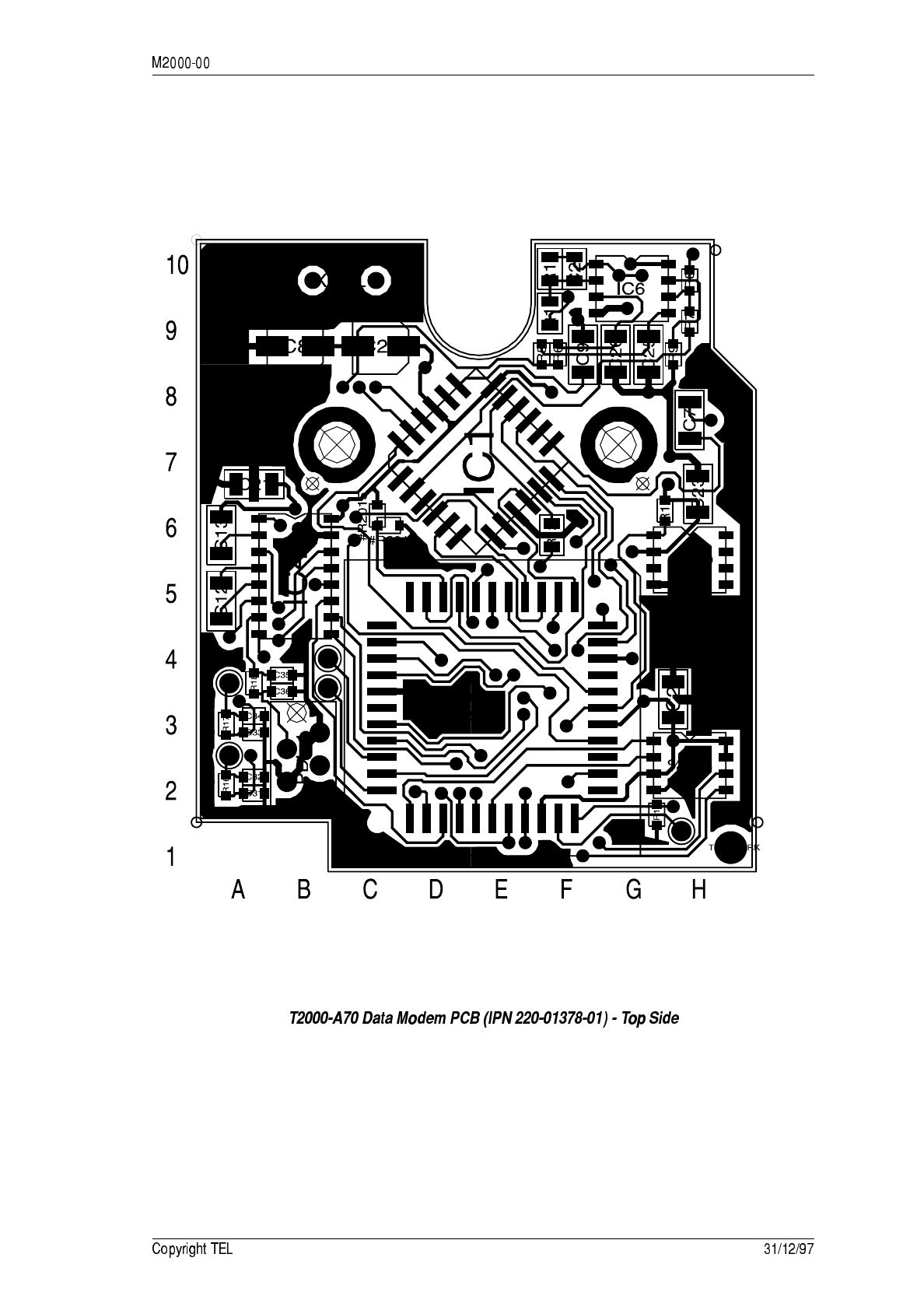
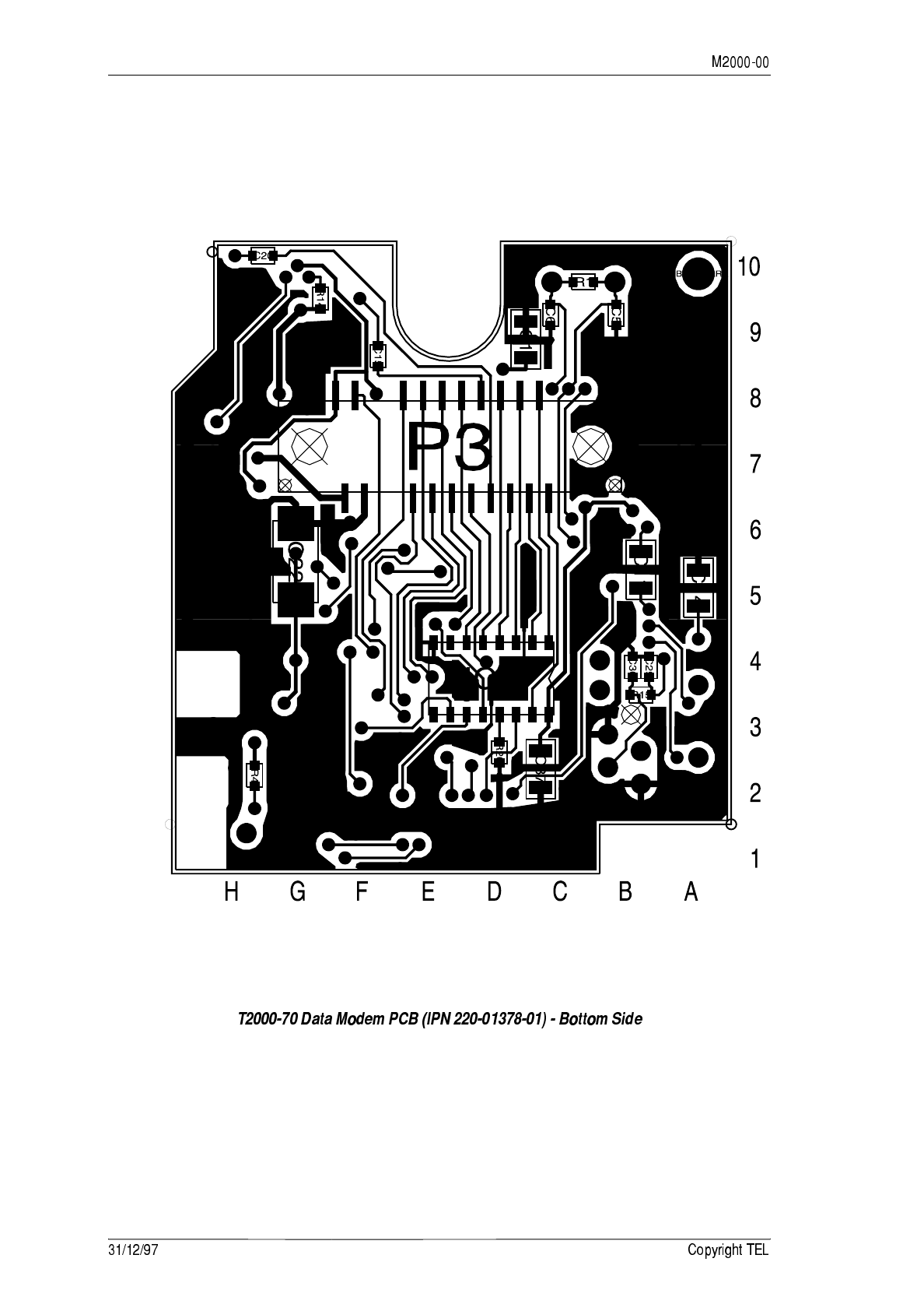
;+#0:;+;2
#*2')
+ !/
#*2')
;+()(=0:;+;2
#*2')
* #*2')
#*2') +

#*2')
-8.8"!&'6') *
* ;C;C;*)#?
The T2000-A03 6m remote loom and T2000-A04 4m remote loom installation kits are for
use with T2020, T2040 and T2050 radios in situations where the 3m remote loom or
underdash mounting is unsuitable.
The T2000-A16 6m shielded remote loom is suitable for use with EMC model radios,
and for installations where electromagnetic radiation may cause problems with sensi-
tive equipment installed nearby or interference to the radio’s own antenna.
Once installed, the loom should not be subjected to any pinching, crushing or chafing,
nor should it interfere with the operation of the vehicle controls.
These instructions must be read in conjunction with Section 3.1 “Servicing Pre-
cautions” and Section 3.2 “Disassembly Instructions”.
The following topics are covered in this Section:
Section Title Page
8.16.1 Components Required 8.13.2
8.16.2 Fitting To Locally Mounted Radios 8.13.2
8.16.3 Fitting To Remote Mounted Radios 8.13.6
* -8.8"!&'6')
* !)6(
The T2000 remote loom kits contain the following components:
* .
&
#
'()(
1Remove the top cover of the radio by unscrewing the 4 bottom cover screws.
Remove the 3 logic PCB retaining screws and fold back the logic PCB. If necessary,
remove the 3 option PCB mounting screws before lifting the logic PCB.
Remove the microprocessor shield retaining screws and the screw securing the
control head ground lead, then remove the microprocessor shield.
Remove the bottom cover of the radio and unplug the loom running between the
control head and the logic PCB (on EMC model radios, the loom runs between the
control head and the EMC filter PCB).
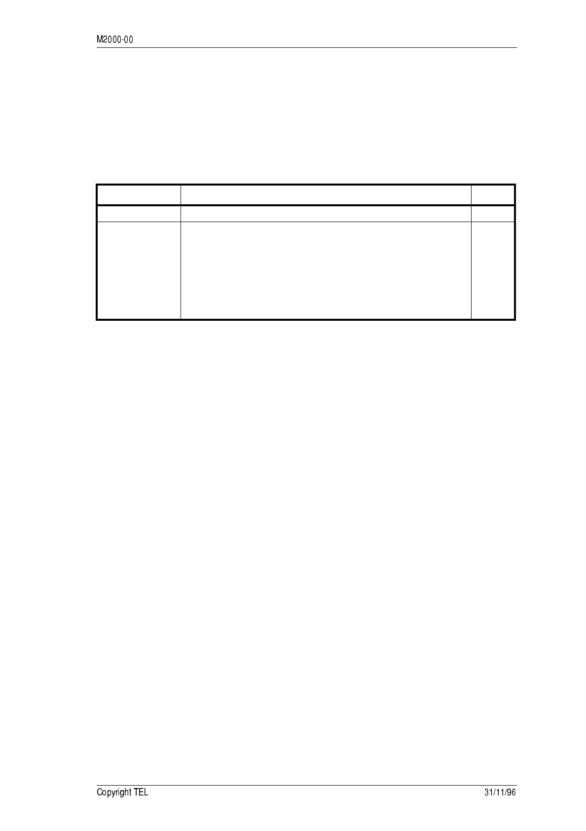
The control head can now be detached from the chassis.
Remove the 4 adaptor plate retaining screws from the control head and remove
the adaptor plate from the back of the control head.
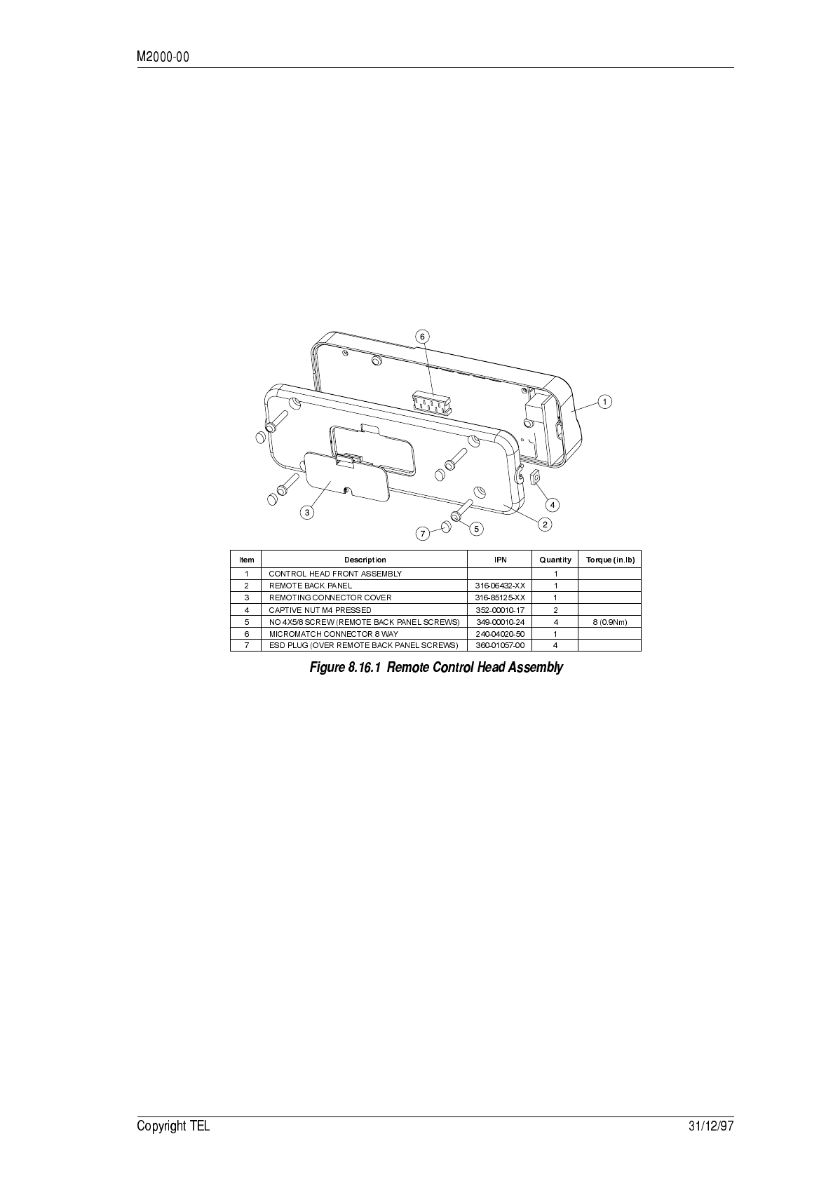
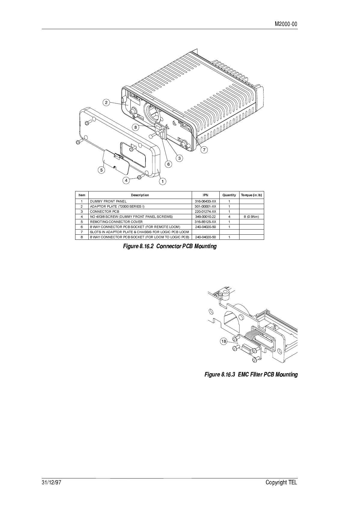
2Refer to Figure 8.16.1.
Unclip the remote back panel remoting connector cover (3).
Pass one end of the remote loom through the connector cover hole and plug onto
the 8 way connector (6) on the top side of the control head PCB.
T2000-A03 & T2000-A04 kits: Remove the ground lead from under one of the con-
trol head PCB screws, and discard the ground lead.
Quantity Description
1 remote loom, complete with 8 way connectors
1 remote mounting bracket
1 remote back panel
1 dummy front panel
2 remoting connector cover (fitted to the remote back panel & dummy front
panel)
2 M4 pressed captive nut (for remote control head assembly)
2 thumbscrew (for remote mounting bracket)
4 ESD plug (to fit over remote back panel screw heads: T2000-A16 only)
2 No 6x3/4 self-tapping screw (for remote mounting bracket)
4 No 4x 3/8 pan Pozi Plastite screw (dummy front panel mounting)
2 M3x6 pan Pozi Taptite screw (connector PCB mounting)
4 M3x8 pan Pozi Taptite screw (EMC filter PCB mounting)
1 EMC filter PCB (Series II radio chassis)
1 connector PCB (Series I radio chassis)
-8.8"!&'6') *
T2000-A16 kit: Remove the screw from the control head that secures the control
head ground lead. Discard the ground lead, and use this screw to secure the
remote loom drain wire solder tag to the control head PCB.
Ensure that the tag does not make contact with any devices in the control head.
3Fit the 2 captive M4 nuts (4) into the slots on the remote back panel (2), and mount
the remote back panel onto the control head front assembly (1).
Secure in place using the 4 No. 4x5/8 Plastite screws previously used for the adap-
tor plate, and push the 4 ESD plugs (7) over the screw heads (T2000-A16 only).
Refit the remoting connector cover, pushing the slot in the cover onto the remote
loom cable.
4 T2000 Series I chassis
Refer to Figure 8.16.2.
Mount the adaptor plate (2) onto the chassis and secure the connector PCB to the 2
chassis pillars, using the 2 M3x6 Taptite screws provided.
As the pillars are not threaded, care must be taken that the screws are not inserted
at an angle.
Pass the logic PCB loom through the slot in the adaptor plate and chassis (7) and
plug the loom onto one of the 8 way connectors (8) on the connector PCB.
Unclip the remoting connector cover (5) from the dummy front panel and pass the
unconnected end of the remote loom through the hole in the dummy head front
panel.
Plug the 8 way remote loom connector onto the 8 way connector (6) on the connec-
tor PCB.
T2000-A16 kit: Secure the remote loom drain wire solder tag under one of the con-
nector PCB screws.
Mount the dummy front panel (1) onto the adaptor plate (2), using the No 4x3/8
Plastite screws (4) provided.
* -8.8"!&'6')
5 T2000 Series II Chassis
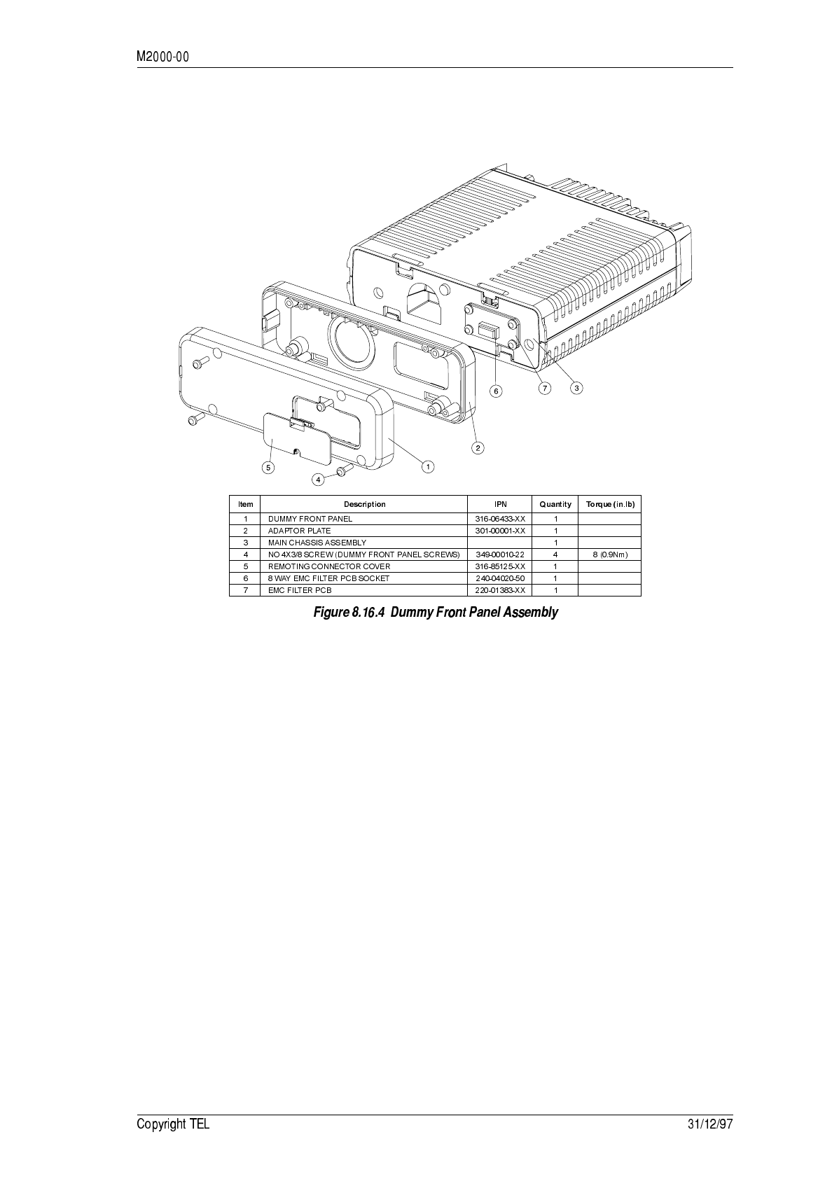
Refer to Figures 8.16.3 and 8.16.4.
Fit the EMC filter PCB (18) provided in the kit to
the chassis, first passing the loom on the bottom
side of the PCB through the chassis hole, as
shown.
Secure the EMC filter PCB in place, using the 4
M3x8 Taptite screws.
EMC model radios will already have an EMC
filter PCB fitted. Check that the top side con-
nector (SKT-1) is 8 way. If not, discard the exist-
ing filter PCB and fit the new PCB provided.
Plug the EMC filter PCB loom onto the logic PCB.
Unclip the remoting connector cover (5) from the dummy front panel (1), and pass
the unconnected end of the remote loom through the holes in the dummy front
panel and the adaptor plate (2).
Plug the 8 way loom connector onto the 8 way connector (6) on the top side of the
EMC filter PCB.
T2000-A16 kit: Secure the remote loom drain wire solder tag under one of the
EMC filter PCB screws.
-8.8"!&'6') *
Mount the dummy head front panel (1) onto the adaptor plate (2), using the 4 No
4x3/8 Plastite screws (4) provided.
Mount the dummy front panel assembly onto the chassis.
6Reposition the bottom cover of the radio and the microprocessor shield and
replace the microprocessor shield retaining screws, tightening them to a torque of
12in.lb (1.4Nm).
Refit the logic PCB, any options PCBs that were fitted and the top cover. Tighten
the top cover to a torque of 15in.lb (1.8Nm).
Refit the remoting connector cover, pushing the slot in the cover onto the remote
loom cable.
7Mount the remote mounting bracket in the desired position (this must be on a flat
surface), using the 2 No 6x3/4 self-tapping screws.
Place the control head in the bracket, positioned for a good viewing angle, and
secure in place with the 2 thumbscrews.

** -8.8"!&'6')
* .
&
)'()(
1Refer to Figures 8.16.2, 8.16.3 & 8.16.4.
Remove the radio dummy front panel (1) by removing the 4 dummy front panel
screws (4).
In later T2000 radios, the radio dummy front panel is fitted with a remoting
connector cover (3). This is unclipped to access the remote loom connector.
When fitting a remote loom, it is therefore unnecessary to remove the dummy
front panel.
Unplug the old remote loom from the connector PCB (Series I chassis) or EMC fil-
ter PCB (Series II chassis).
Series II chassis: Check that the top side connector (SKT-1) on the EMC filter PCB
is 8 way. If not, discard the existing filter PCB and fit the new PCB provided in the
kit (refer to Section 8.16.2, “Fitting To Locally Mounted Radios”, step (5)).
If necessary, replace the old dummy front panel with the new dummy front panel,
complete with remoting connector cover, provided in the kit.
Pass the new remote loom through the connector cover hole in the dummy front
panel, and plug the 8 way remote loom connector onto the 8 way connector (6) on
the connector PCB or EMC filter PCB.
T2000-A16: Fit the remote loom drain wire solder tag under one of the connector
PCB or EMC filter PCB screws.
Mount the dummy front panel onto the adaptor plate (2), and secure in place
using the 4 dummy front panel screws.
Refit the remoting connector cover, pushing the slot in the cover onto the remote
loom cable.
2Refer to Figure 8.16.1.
Remove the control head remote back panel (2) by removing the 4 remote back
panel screws (5), taking care not to loose the captive nuts (4). EMC model radios
will also have ESD plugs (7) over the remote back panel screws.
In later T2000 radios, the control head remote back panel is fitted with a remot-
ing connector cover (3). This is unclipped to access the remote loom connector.
When fitting a remote loom, it is therefore unnecessary to remove the remote
back panel.
Unplug the old remote loom from the 8 way connector on the control head PCB (6).
If necessary, replace the old remote back panel with the new remote back panel,
complete with remoting connector cover, provided in the kit.
Pass the new remote loom through the connector cover hole in the remote back
panel, and plug the 8 way connector on the new remote loom onto the 8 way con-
nector on the control head PCB.
T2000-A16: Fit the remote loom drain wire solder tag under one of the control
head PCB screws.
Ensure that the solder tag does not make contact with any devices in the control
head.

-8.8"!&'6') *+
Fit the 2 captive M4 nuts into the slots in the remote back panel and mount the
remote back panel onto the control head front assembly (1).
Secure in place using the 4 remote back panel screws, and push the 4 ESD plugs
(7) over the screw heads (T2000-A16 only).
Refit the remoting connector cover, pushing the slot in the cover onto the remote
loom cable.

* -8.8"!&'6')
3 -
-
This Section outlines the production software history for each T2000 Series II model,
and explains how to identify which software version is used.
The following topics are covered in this Section:
Section Title Page
9.1 Identifying The Software Version Number 9.2
9.2 Software History 9.3
9.2.1
9.2.2
9.2.3
9.2.4
9.2.5
9.2.6
T2010 & T2015 Radios
T2020 Radios
T2030 & T3035 Radios
T2040 Radios
T2050 Radios
T2060 Radios
9.3
9.4
9.5
9.6
9.7
9.8
- 3
- (&$%:3
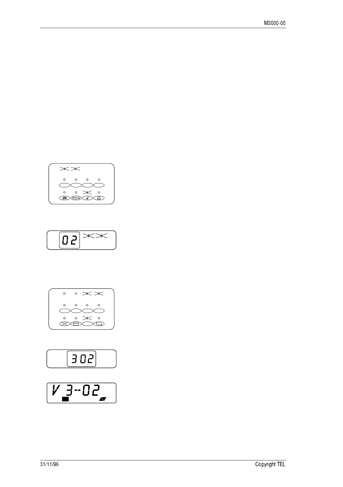
To read the radio software version of a T2000 Series II radio, hold in the PTT switch
when turning on the radio. The version number will then be displayed briefly on the
radio’s front panel, using either the LEDs, the 7 segment display panel or a combination
of both.
Where LEDs are used, they indicate Binary Coded Decimals (BCDs), with the most sig-
nificant bit to the left.
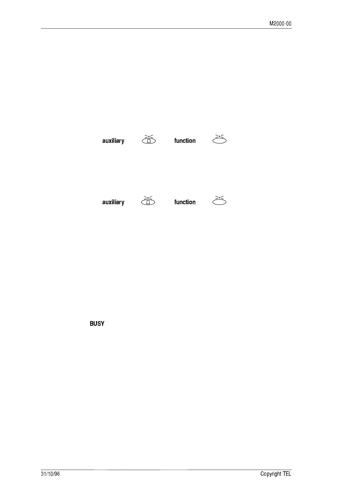
The examples below show how each radio displays “Version 3.02”.
:" This is not necessarily a valid radio software version.
• The major version number is indicated as a BCD by the
Busy and Tx LEDs. (“3” in the example on the right.)
• The two digit minor version number is indicated as
BCD digits by the two lower rows of LEDs. (“0” on the
middle row and “2” on the lower row in the example.)
<*
• The major version number will be indicated as a binary
coded decimal (BCD) by the Busy and Tx LEDs.
• The minor version number is shown in the two digit
display.
• The major version number is indicated as a binary
coded decimal (BCD) by the top row LEDs.
• The two digit minor version number is indicated as
BCD digits by the two lower rows of LEDs.
• The full version number is shown in the display.
AA
• The full version number is shown in the display.
1234
BUSY
TX
BUSY TX
C1 C2 C3 C4
Fn
SVC WAIT GO TX
BUSY
TX
WAIT
3 -
- >
The following tables outline the production software history for each T2000 Series II
radio.
:" Previous revisions of the software cannot be used on Series II radios.
- < )(
Radio
Software
Version
Release
Date PGM Software
Compatibility Changes From Previous Version
2.20 6/12/96 PGM201X v1.22 Original
- 3
- )(
Radio
Software
Version
Release
Date PGM Software
Compatibility Changes From Previous Version
5.10 13/12/96 PGM2020 v2.31 Original
3 -
- < )(
Radio
Software
Version
Release
Date PGM Software
Compatibility Changes From Previous Version
3.10 6/12/96 PGM203X v1.34 Original
-* 3
- )(
Radio
Software
Version
Release
Date PGM Software
Compatibility Changes From Previous Version
5.20 6/12/96 PGM2040 v2.45 Original
3 -+
- )(
Radio
Software
Version
Release
Date PGM Software
Compatibility Changes From Previous
Version
Non-Trunked Trunked
1.05 13/3/96 PGM2020 v2.31 PGM2040 v2.45 Original

- 3
-* *)(
Radio
Software
Version
Release
Date PGM Software
Compatibility Changes From Previous Version
1.04 28/11/96 PGM2060 v1.03 Original