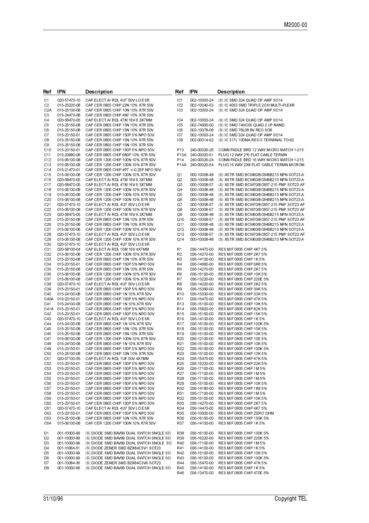
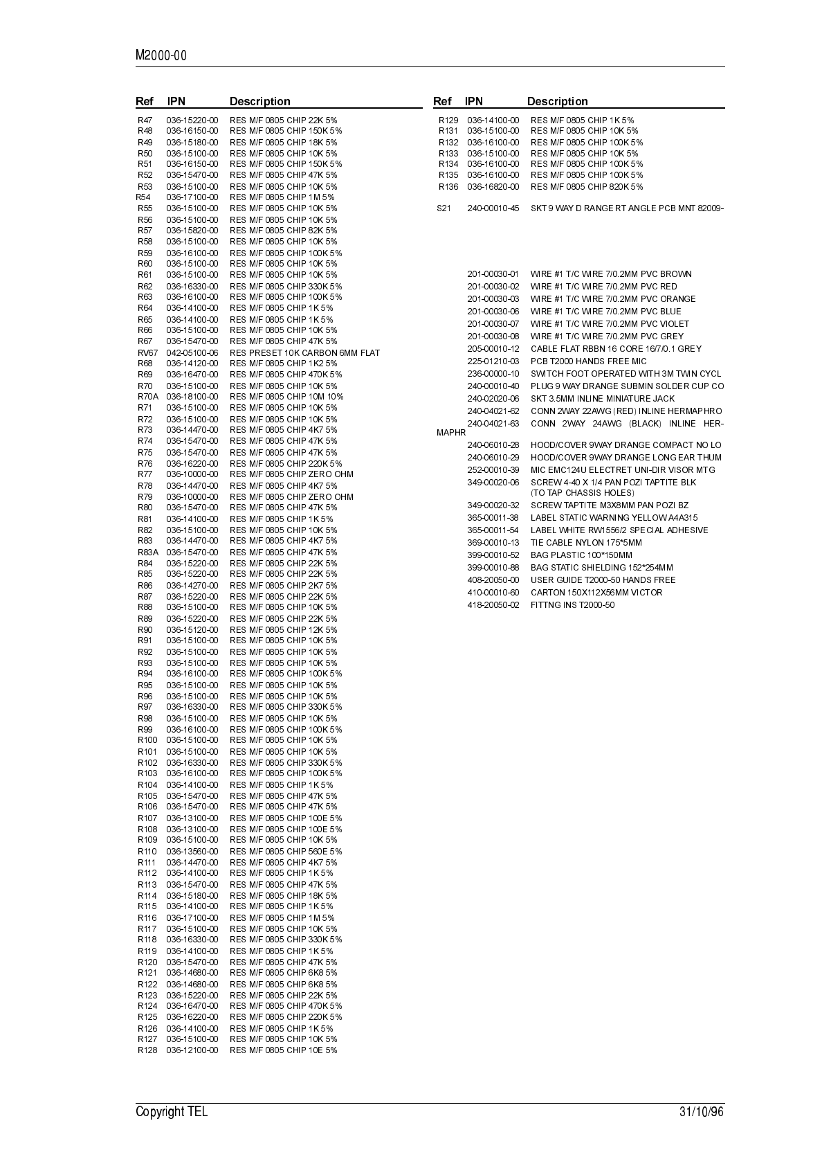
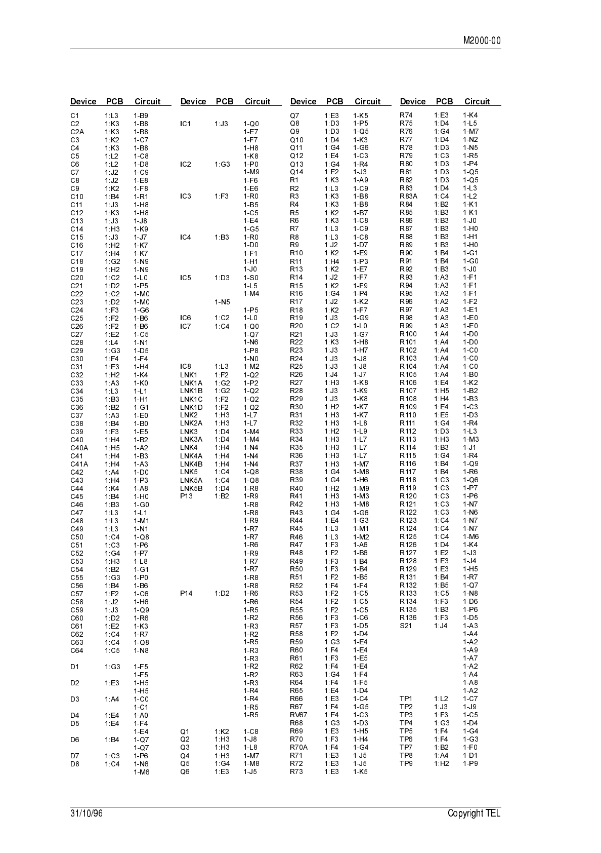
Contents
user manual part 5
This Section provides information on T2000 Series II accessories.
The following accessories are covered in this Section:
Section Title PCB IPN Page
8.1 T2008 Power Supply 220-01170-03 8.1.1
8.2 Connection To External Devices 8.2.1
8.3 T2000-500 & T2000-600 1-7W Versions 8.3.1
8.4 T2000-05 Remote Speaker Kit 8.4.1
8.5 T2000-A06 Desktop Microphone Kit 8.5.1
8.6 T2000-A07 DTMF Microphone Kit 8.6.1
8.7 T2000-34 Selcall Kit 8.7.1
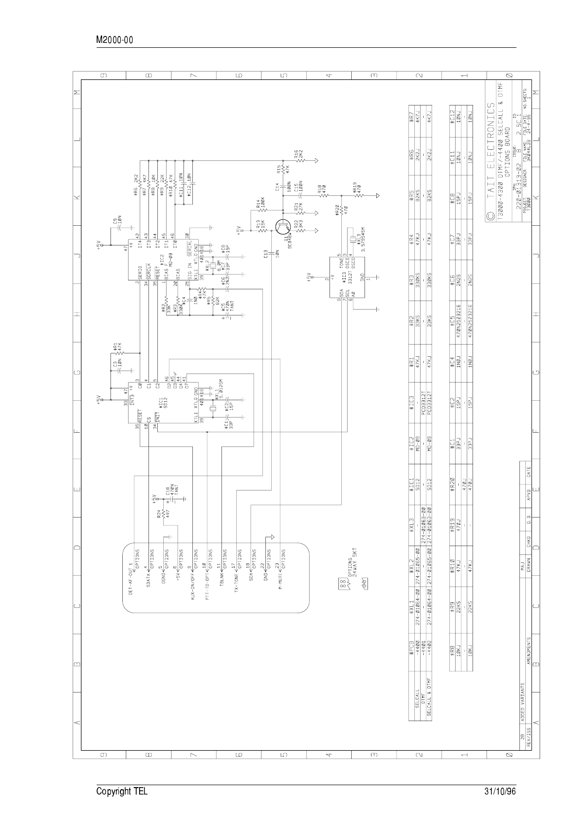
8.8 T2000-A36 Selcall Kit 220-01313-02 8.8.1
8.9 T2000-40 DTMF Kit 8.9.1
8.10 T2000-A450X CTCSS & Scrambler Kits 220-01335-04 8.10.1
8.11 T2000-A50 Handsfree Kit 225-01210-03 8.11.1
8.12 T2000-A60 Dual Port UART Kit 220-01251-01 8.12.1
8.13 T2000-A66 Single Port UART Kit 220-01348-04 8.13.1
8.14 T2000-A80 Line Interface Kit 220-01272-02 8.14.1
8.15 T2000-A70 Data Modem Kit 220-01378-01 8.15.1
8.16 T2000-A03/-A04/-A16 Remote Loom Kits 8.16.1

The following topics are covered in this Section:
Section Title Page
8.1.1 Operation 8.1.2
8.1.2 Performance Specifications 8.1.3
8.1.3 Precautions 8.1.5
8.1.4 Circuit Operation 8.1.6
8.1.5 Installation 8.1.8
8.1.6 Introduction To Servicing 8.1.10
8.1.7 Setting Up The Power Supply 8.1.12
8.1.8 Fault Finding 8.1.14
8.1.9 Repair 8.1.15
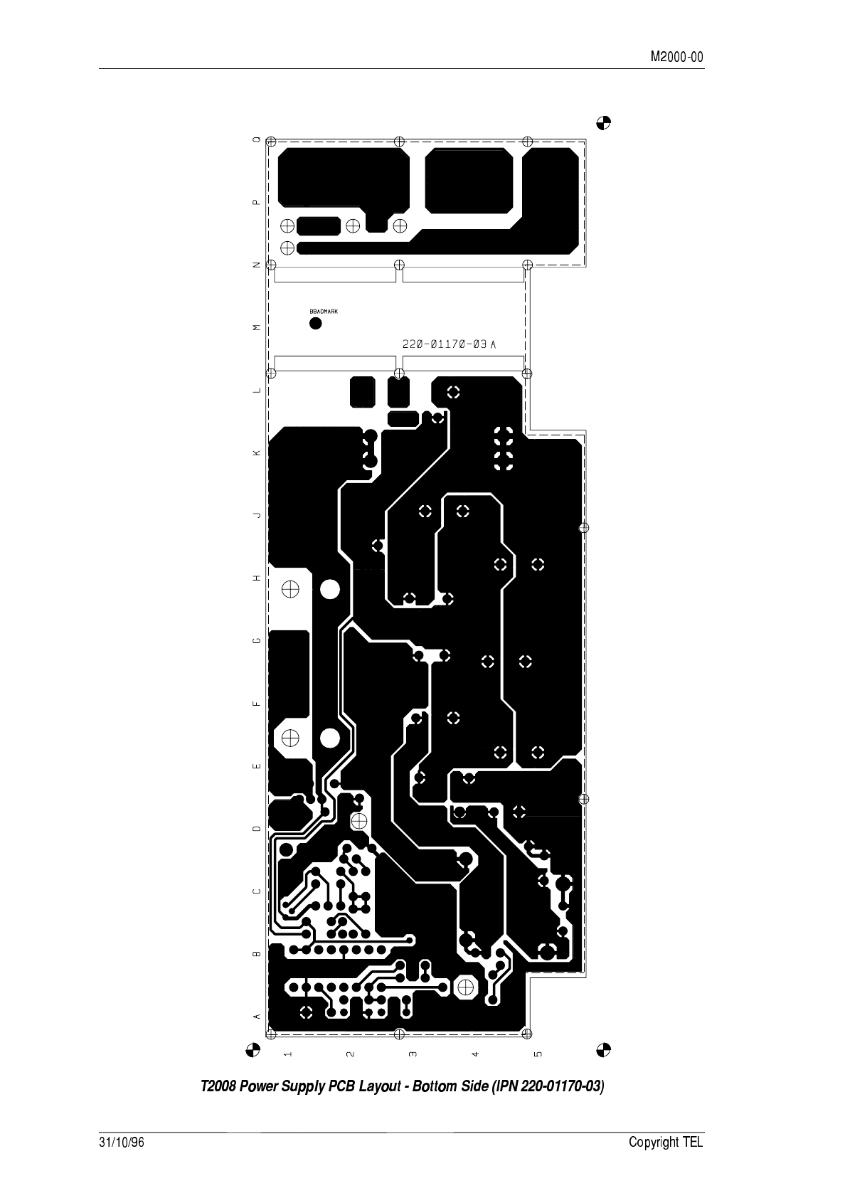
8.1.10 PCB Information 8.1.17

The T2008 Power Supply is a mains operated power supply designed to provide the DC
supply requirements of the T2000 Series II radios. It uses switch mode technology to
control the regulation of the output voltage, which results in a power supply with a
higher temperature rating, improved efficiency and greater reliability.
The power supply can either be operated with the radio sitting on top as a desk top unit,
or with the radio and power supply detached as two separate units (refer to Section
8.1.5, “Installation”).
The T2008 has protection circuits for overcurrent, overtemperature and overvoltage pro-
tection circuitry. Current limiting is included to restrict the peak current to about 9.5A.
In addition, a self-restoring thermal shutdown keeps the temperature of the switching
transistor within the ‘safe operation area ratings’. The point of thermal shutdown is also
dependant on the load current, to allow for a higher duty cycle rating at lower output
currents. The output voltage and thermal shutdown points are factory preset.
The power supply also has a limited capability to float charge a lead acid battery under
constant voltage conditions (refer to Section 8.1.5, “Installation”).

T2000-21, -23, -24:
Voltage .. 230V ±10% (limits: 207-253V AC)
Frequency .. 50Hz
T2000-22:
Voltage .. 115V ±10% (limits: 105-130V AC)
Frequency .. 60Hz
Power .. 200VA maximum
(mains input +10%, current limited output)
Mains Supply Plug:
T2008-21 .. New Zealand
T2008-22 .. USA
T2008-23 .. UK
T2008-24 .. European
Voltage .. 13.8V DC (adjustable 12.5 to 14.5V)
Current:
Intermittent Operation .. 6.5A at 33% duty cycle (maximum 2
(TA = 25°C, input 230V) minutes on)
Peak Rating .. 8A max. (duration limited by thermal
shutdown)
Continuous Rating .. 4.5A maximum
(TA = 25°C, input 230V)
Voltage Regulation .. ±5%
(supply variation ±10%, currents up
to 6A, temp. range -10°C to +60°C)
Current Limiting (TA = 25°C) .. 9.5A nominal
(10A secondary fuse available)
Overvoltage .. 16V ±5% by zener transient
suppression diode (not self-restoring)
Thermal Overload .. shutdown occurs at approximately
(‘cold’ start @ 25°C, input = 115/230V) 95°C heatsink temperature (7A
continuous after 1 hour)

Input:Primary Fuse:
T2008-21, -23, -24 .. 1A time delayed
T2008-22 .. 3A
Thermal Cutout .. integral with transformer
Ripple and Noise .. less than 10mVrms
0 to 6.0A, mains voltage ±10%
Operating Temperature Range .. -10°C to +40°C
Weight .. 3.0kg
Dimensions:
Height .. 95mm
Length .. 225mm
Width .. 150mm
!"#$%&
The power supply contains voltages that may be lethal. The unit should not be disman-
tled without first disconnecting the mains supply. Servicing should be carried out only
by qualified technicians.
!"%
If the power supply is operated at high output currents and/or a high duty cycle rate
for a prolonged period of time (e.g. more than 10 minutes), the heatsink will become
very hot. Do not touch.
Do not operate the power supply in a sealed cabinet. Ensure that there is an adequate
airflow past the unit, and in particular past the heatsink at the back of the unit.
!"'!(
If the mains supply cord needs replacing, it must be replaced with a mains supply cord
of the same size and type as originally fitted.
!"
When using a T2008 and radio at a fixed location, it is advisable to check the maximum
allowable transmit power, as defined by the local radio regulatory authority. This is
commonly in the range of 1 to 5W, and exceeding this output power may result in pros-
ecution.
!"!)&
If the duty cycle (33%) of the radio and power supply is likely to be exceeded, then the
radio output power must be reduced to ensure that the current drawn from the power
supply does not exceed its rating.
It is advisable to check the current drawn from the power supply, regardless of duty
cycle, if the radio is operated at full power (25W). Variations in antenna VSWR can
result in current drain, which may exceed the rating of the supply.

*
!
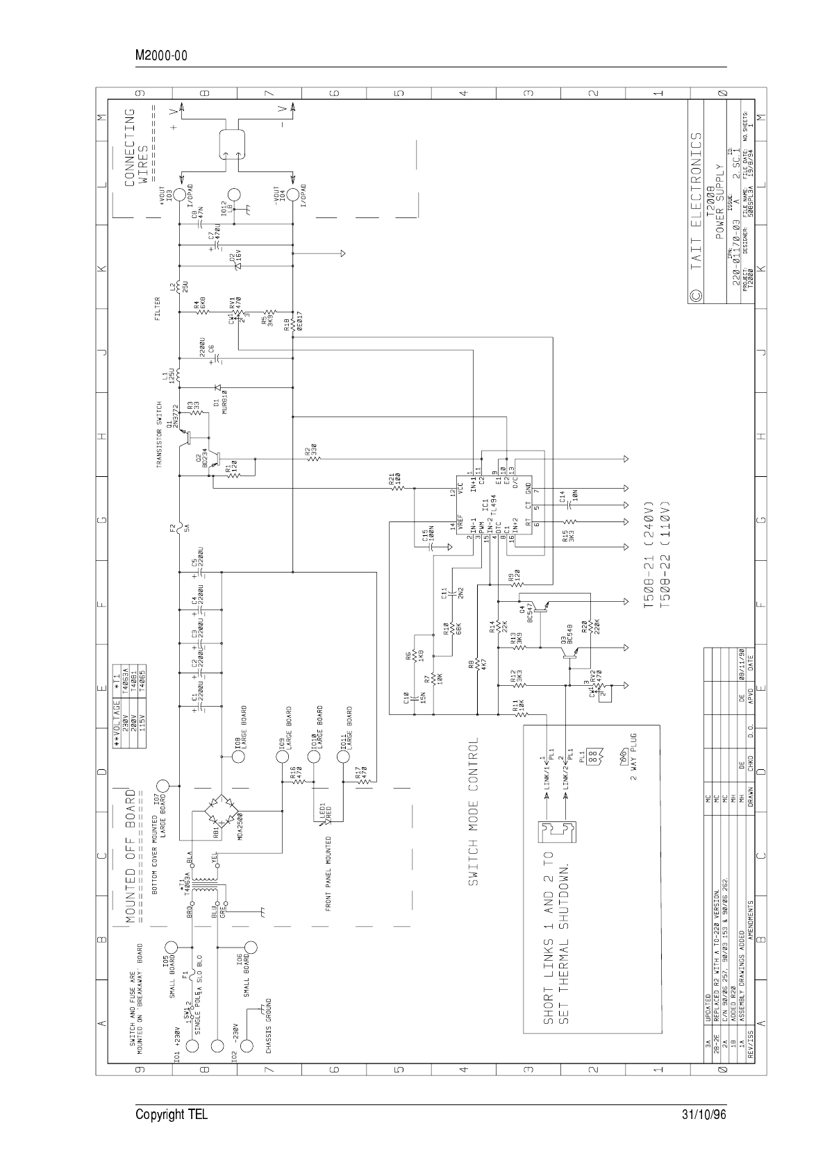
Refer to the diagram to the rear of this Section.
)
The mains supply is connected to the primary of the transformer via the supply cord,
input fuse and on/off switch.
A conventional bridge rectifier is used across the secondary winding of the transformer,
with both positive and negative leads being isolated from earth. Five PCB mounted
smoothing capacitors are used to produce a 23V DC bus from the 18Vrms secondary of
the transformer. The ripple on the DC bus is 4V peak to peak, with an output current of
6A.
The front panel LED is illuminated when mains power is applied.
$
Voltage regulation is provided by the complementary Darlington configuration of Q1
and Q2. The switching of this pair is derived directly from IC1 (TL494).
When Q1 is turned on, current flows in inductors L1, L2 and L3 to supply the output.
Capacitors C6 and C7 hold the output voltage at a nominal 13.8V. When Q1 turns off,
the current flowing in the inductors continues to flow, via diode D1.
C8, C9 and L3 form a common mode filter to suppress conducted noise at the output.
!!
A pulse width modulating IC (IC1) controls the switching of Q1 and thus the regulation
of the output voltage. A voltage divider (R4, R5 and RV1) converts the output voltage to
a 5V nominal level. It is then compared to IC1s temperature compensated internal 5V
reference. The length of time Q1 is turned on is proportional to the difference between
the reference and the output voltage. Feedback compensation is provided by C10, C11,
R6 and R7, while R10 improves the transient response for the feedback circuit.
!#&
Current limiting is provided by monitoring the voltage across the current sense resistor
(R18). When the current is increased to approximately 9.5A, the voltage on pin 15 of IC1
decreases to a point where the pulse width of the switching waveform decreases. In
addition, a 10A fuse is provided in the secondary circuit of the power supply.

+
,%&
Overvoltage protection is provided by diode D2 and fuse F2. D2 is a 16V zener transient
suppression diode that reacts instantly to overvoltage DC or spikes. If an overvoltage
condition persists, causing excessive power dissipation in D2, it will become short cir-
cuit, causing F2 to blow. F2 will need to be replaced before operation of the power sup-
ply is possible. D2 will need to be replaced to restore overvoltage protection.
$$(
Transistor Q3 is mounted on the heatsink and its junction temperature therefore closely
follows that of both the heatsink and Q1. Q3 is biased by R12 and RV2. As the tempera-
ture of the heatsink increases, the temperature of the base- emitter junction of Q3 also
increases, which results in the Vbe of Q3 decreasing. At 95°C, the base-emitter voltage is
exceeded by the biasing voltage, and Q3 switches on. As a result, Q4 turns off, and the
‘deadtime pin’ (pin 4 of IC1) is pulled high. The ‘deadtime’ is now 100%, which means
Q1 is completely turned off.

The T2008 power supply is designed to provide the DC supply requirements of the Tait
T2000 two way radios. It can be operated either with the radio sitting on top as a desk
top unit, or with the radio and power supply detached as two separate units. The bot-
tom case includes two screw recesses for wall mounting. The two way radio then can be
mounted in its cradle next to the supply, or operated away from it, e.g. on a desk top,
etc.
If the radio and the power supply are operated away from each other, an extension cable
for the DC supply would have to be used. To keep the voltage drop of this extension
cable reasonably low, the wiring should be of sufficient gauge to carry the required load.
It is recommended that a minimum wire size of 1.5mm is used.
The power supply requires a mains supply of 230V nominal 50Hz or 115V nominal
60Hz, as set out in Section 8.1.2.
If the power supply is run at a high duty cycle rate, high continuous output currents
and/or high mains input voltage, it will generate a considerable amount of heat. An
adequate flow of cooling air past the unit, particularly past the heatsink, is therefore
essential for reliable operation. Do not operate the power supply in a completely
enclosed cabinet.
Do not touch the heatsink after prolonged heavy duty operation. Keep the
heatsink away from anything affected by heat (plastics, etc).
The microphone clip supplied with every power supply may be attached to the side of
the top cover with the supplied screws and spacer, which fits between the clip and
cover. The hook switch monitor wire should be connected as shown in the wiring dia-
gram.
-
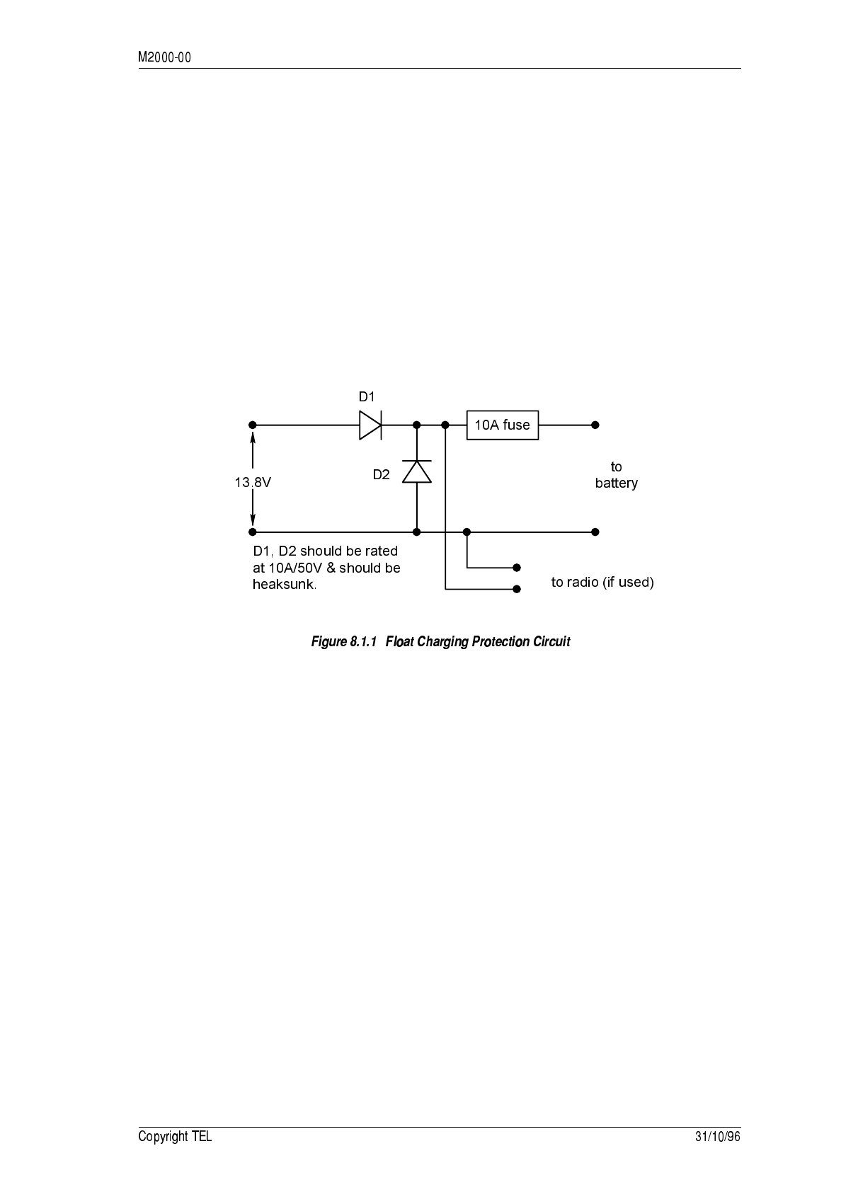
.!$&&#((/
The power supply has a limited capability to float charge a lead acid battery under con-
stant voltage conditions. The performance is limited by the way the power supply’s
continuous output current rating is limited (typically 4.5A at 20°C).
The following diagram shows an external protection circuit, consisting of two diodes
with the appropriate ratings (i.e. 10A/50V), to be used when float charging a lead acid
battery. This circuit prevents damage to the power supply due to reverse current, or the
battery being connected with reverse polarity.
The current limit prevents charging from being excessive, should a discharged battery
be connected. The output voltage of the power supply does not compensate for the tem-
perature dependence of lead acid batteries.
* (,
&
All sub-assemblies within the T2008 power supply (e.g. transformer, PCB/heatsink) are
housed in a specially moulded plastic case with no screws. The top and bottom halves
of the plastic case are fastened by four self-tapping screws.
All electrical components except the transformer and LED are mounted on either the
larger regulator/heatsink PCB or on the smaller mains input PCB.Disassembly
Disconnect the unit from the mains supply before attempting to remove
the top case.
!"#$%&
The power supply contains voltages that may be lethal. The unit should not be disman-
tled without first disconnecting the mains supply. Servicing should be carried out only
by qualified technicians.
!"%
If the power supply is operated at high output currents and/or a high duty cycle rate
for a prolonged period of time (e.g. more than 10 minutes), the heatsink will become
very hot. Do not touch.
Do not operate the power supply in a sealed cabinet. Ensure that there is an adequate
airflow past the unit and in particular past the heatsink at the back of the unit.
!"'!(
If the mains supply cord needs replacing, it must be replaced with a mains supply cord
of the same size and type as originally fitted.
),$!
Turn the unit upside down and remove the two self-tapping screws.
Turn the unit back on its feet and remove the two top screws.
Carefully lift the top case away from the unit.
All the sub-assemblies are now easily accessible, and can be lifted out as neces-
sary.

)$$&012
Unsolder the leads of the transistor using solder wick or a solder sucker.
Remove the appropriate screws and carefully lift off the transistor.
Mount the new transistor using a silicon insulating gasket on the underside. Do
not use any other insulators (mica, etc) as they are unlikely to fit under Q1 and/or
would require thermal compound.
Refit the two screws for Q1 from the copper side of the PCB. Isolate each of these
two mounting screws from touching the heatsink with a 3mm length of silicone
rubber sleeving. Use spring washers under the two nuts.
Carefully position the PCB onto the heatsink before tightening the two screws/
nuts.
Ensure that Q3 sits firmly against the walls in its slot on the heatsink.
Resolder the leads of the transistor.
)3
Reassembly is carried out in the reverse order to disassembly.

+
&
4$
56)6(
• Ammeter: 10A DC
• Voltmeter: 0 - 20V DC
• Load Resistor: 0 - 100Ω, 10A (variable)
• Short circuit plug-in link: IPN 240-04020-62
• Ohmmeter: infinity to 0Ω
Refer to the T2008 circuit and wiring diagrams to the rear of this Section.
Check with the ohmmeter that the heatsink is electrically isolated from the nega-
tive output.
Connect the variable load in series with the ammeter across the output terminals
(see wiring diagram for the pin configuration of the output plug).
Set the load to maximum resistance (minimum load current).
Connect the DC voltmeter across the power supply output terminals.
The DC output wiring should be of sufficient gauge to carry the load current
required. It is recommended that a minimum wire size of 1.5mm is used.
Plug in the mains connector.
%&
Switch on the power supply.
Set RV1 for an output voltage of 13.8V.
Switch off the power supply.
$$(072
Before setting up the temperature shutdown, ensure that the power supply is at
ambient temperature, i.e. it has not been running recently with any significant
load current. The temperature shutdown is based on a heatsink ambient tempera-
ture of 25°C.
Disconnect the load resistor.

Insert the plug-in link (1 - 2).
Switch on the power supply.
Set RV2 (TSD) so that the power supply just shuts down.
Switch off the power supply.
Remove the plug-in link.
!#
Reconnect the load resistor.
Switch on the power supply.
Decrease the load resistance (current rises) and set it for an output current of
approximately 9.5A.
Decrease the load resistance and the voltage output should drop, indicating that
current limiting is in progress.
If the power supply is very hot, the current limit circuit may cause the unit to
switch off completely. If this occurs, switch off the mains supply and wait
approximately one minute. The power supply should now operate normally.
..(
&
The checks listed below have been included to provide assistance in locating faults. It is
sometimes convenient to disable a complete section of the power supply in order to iso-
late a fault. If individual sections are isolated the rest of the unit should operate nor-
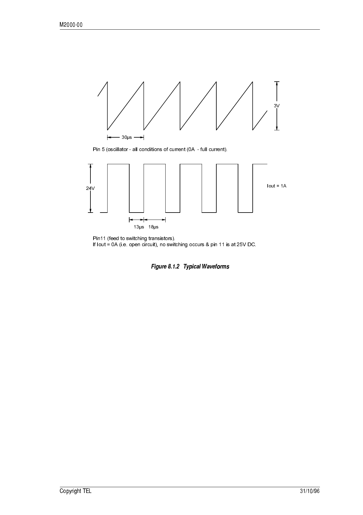
mally (refer to Figure 8.1.2, “Typical Waveforms” for details).
!!$8
Faulty diodes and transistors can generally be found by a simple ohmmeter check, as
follows (an AVO model 8 or equivalent meter should be used for taking the measure-
ments, using only the medium or low resistance ranges):
Set the ohmmeter to the ohms x 1 range.
Measure the forward and reverse resistance of each junction. The resistance in one
direction should be low (generally 30 to 100Ω), and the resistance in the other
direction should be high. In a faulty transistor or diode, the junctions will usually
be either short or open circuited.
Other components in the circuit may affect these readings unless the junctions
are isolated.
The collector current drawn by multijunction transistors is a further guide to their oper-
ating performance.
%&
The following table shows voltages under normal operating conditions, and those fol-
lowing thermal shutdown:
Normal Operation
(V) Thermal Shutdown
Operating (V)
output voltage 13.8 0
Q3 base-emitter voltage 0.2 approx. 0.7 approx.
Q4 base-emitter voltage 0.7 approx. 0 approx.
IC1 pin 4 voltage 0 5
IC1 pin 14
(voltage reference) 55
9,
The following waveforms can be expected under the stated conditions.
- )
The T2008 power supply requires specialised component replacement techniques.
Before attempting repair, refer to Section 3.4, “Repair”.

*
#0:;+;2
+
!/
'$<'
-
()(=0:;+;2
IC1
To I012
- Out
- Out
+ Out
4 Way Power
Connector
to T 500 Radio
Ext. Speaker Ext. Speaker
Live
7 way Power
Connector to
T2000 Radio
Internal
Speaker
+ Out
Gnd
To Mic
Clip
To Mic Clip
Earth Mains
Green/Yellow
Earth Shield
Transformer
Green
Ferrite
Bead
Mains
LED Red
LED Black
Yellow
Transformer
Secondary
Black
Yellow
Black
Black (-)
Output Voltage Set
Thermal
Shutdown
Set
Blue
Blue
Green
Green
Brown
Brown
Primary
Fuse
F1
Mains
Switch
Transformer
T4063
Secondary
Red (+)
LED
E
C7
C5
C4
C2
~
-
~
+

!5=7,
(
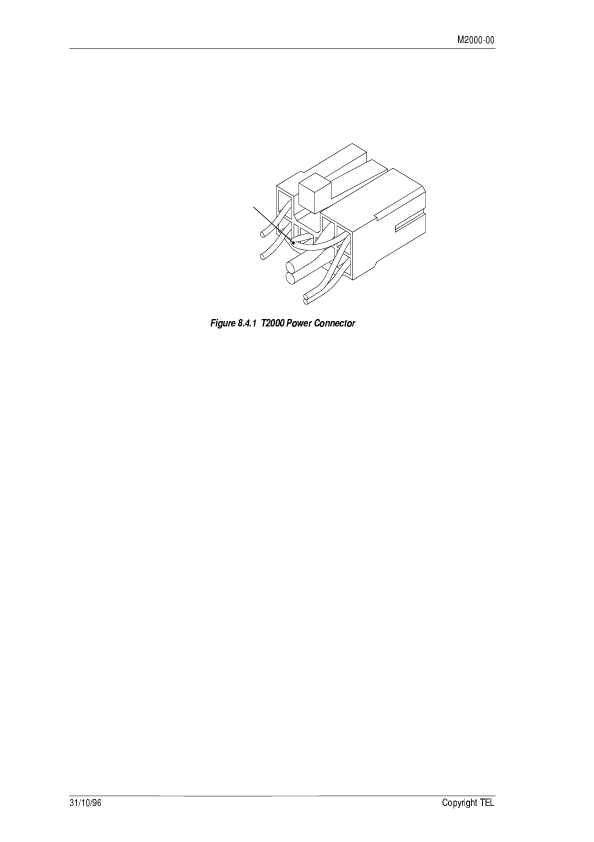
The spare external pin in the T2000 power connector (refer to Figure 8.4.1) may be wired
to any of the option connections tabled in Section 5.9, “Options Interface Specifications”.
The most commonly used connections (hush, horn, emergency and auxiliary), are
explained below.
The T2010 and T2015 can be programmed to have channel selection controlled via S15
on the T2000 logic PCB.
>$
An active +5V signal is supplied to this line each time the PTT is pressed or a valid
transmission is received (i.e. audio is heard), and is commonly used to mute a car radio.
It may be connected directly to some modern stereo systems, otherwise an interface
device will be required. This signal is sometimes referred to as the ‘external mute’.
>
This is used in a Selcall system where an external alert has been programmed. An active
+5V signal is supplied to this line when the radio goes into the external alert cycle. This
signal will either be pulsed, steady or ringing, depending on the radio model and pro-
gramming.
5&
This is used to put the radio into emergency mode for a Selcall system and is activated
when the input is switched to ground.
=
An active +5V signal is switched to this line when the front panel
key (T2010, T2015 & T2020 models) or key (trunked models) is
active. This is programmable with both latching and momentary operation available.
Fn

!
The spare external pin in the power connector is connected to an option by linking the
appropriate option pin to the EXTERNAL pin on options connector S14 (refer to Section
5.9, “Options Interface Specifications”).
The recommended linking method is to crimp a short length of 7/0.2mm PVC wire
between the appropriate connections on a 16-way Micromatch plug (IPN 240-00026-24),
which can then be plugged onto the options connector.
< /!7
The front panel keys do not function when the T2010 or T2015 is programmed for chan-
nel selection control via the BCD lines.
Access to the BCD lines is via S15 on the logic PCB. Refer to Section 5.9, “Options Inter-
face Specifications” details.
!"#$%
; <;*;+9%
This Section describes how to convert a T2000-500 or T2000-600 radio to operate
between 1 and 7W.
T2000-500 and T2000-600 1 to 7W radios are currently type approved only in
Australia and Germany.
The following topics are covered in this Section:
Section Title Page
8.3.1 Components Required 8.3.2
8.3.2 Fitting 8.3.2
8.3.3 Set-Up 8.3.4
8.3.4 Specifications 8.3.4
!"#$%
!)6(
To convert a T2000-500 and T2000-600 to low power, the following components are
required:
.
&
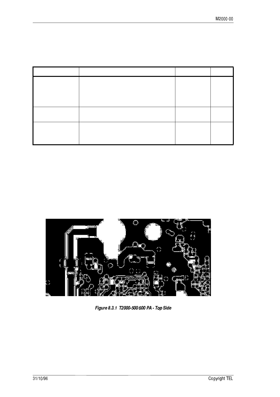
1Refer to Figure 8.3.1.
Remove L315, L316, L317 and *R319 from the top side of the PA.
Crush and remove the ferrite bead which forms part of L314, so that only the wire
link remains.
Description IPN Quantity
Low Power
Common Parts 56Ω SRF16 resistor 030-02560-20 2
T2000-500/600 replacement transistor PCB 220-01287-00 1
radio type label - 1
appropriate type approval label - 1
T2000-500 Low
Power Parts 5p6 NP0 500V GRM42-2 chip capacitor 015-01560-06 2
22p NP0 500V GRM42-2 chip capacitor 015-02220-06 3
T2000-600 Low
Power Parts 4p7 NP0 500V GRM42-2 chip capacitor 015-01470-06 1
5p6 NP0 500V GRM42-2 chip capacitor 015-01560-06 1
18p NP0 500V GRM42-2 chip capacitor 015-02180-06 2
L315
*R319
*L316
L314
L317
*C330
*C331
*C332
C300
C346
Replacemen
t
zero Ω
resistor
Q308
!"#$%
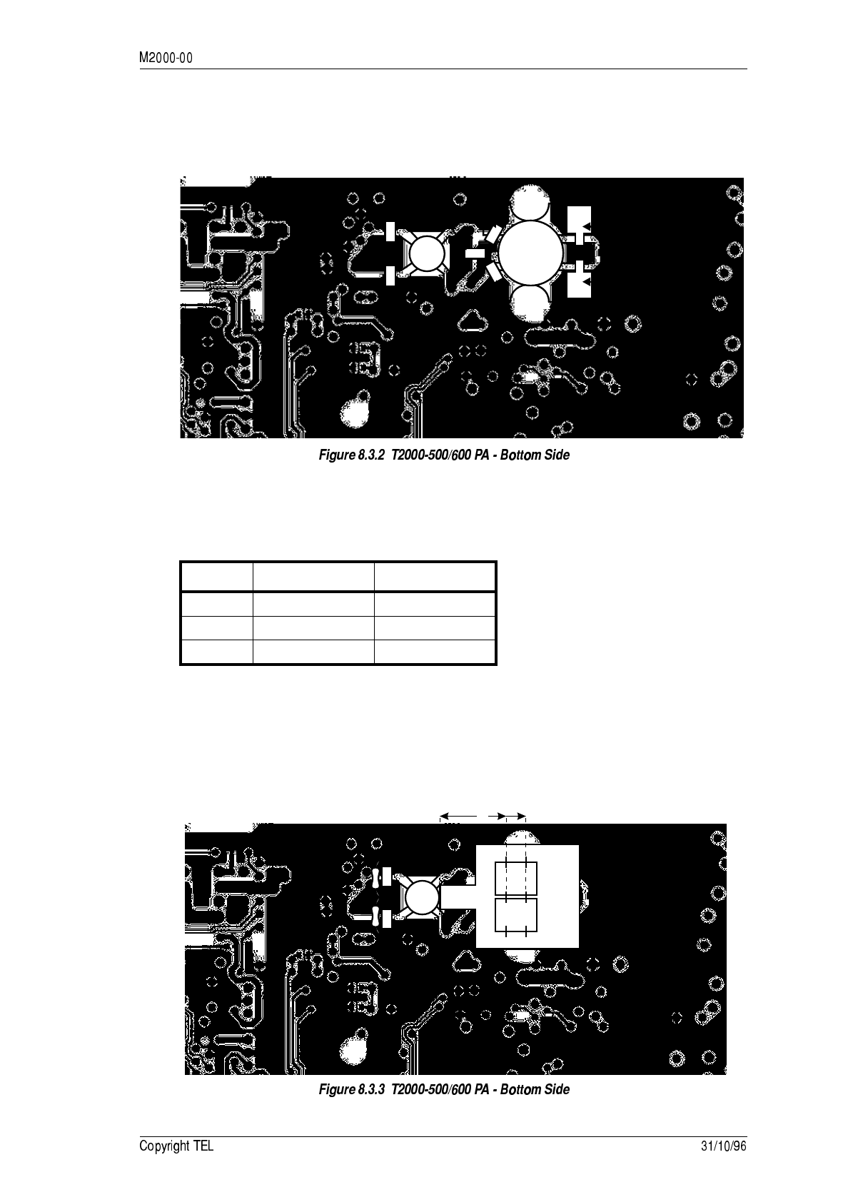
2Refer to Figure 8.3.2.
Remove the following components from the bottom side of the PA:
C323, *C324, C325, *C327, *C329 and Q306.
3Remove the output matching capacitors, *C330, C331 and *C332 from the top side
of the PA (shown in Figure 8.3.1).
Solder the replacement capacitors in the original positions, as follows:
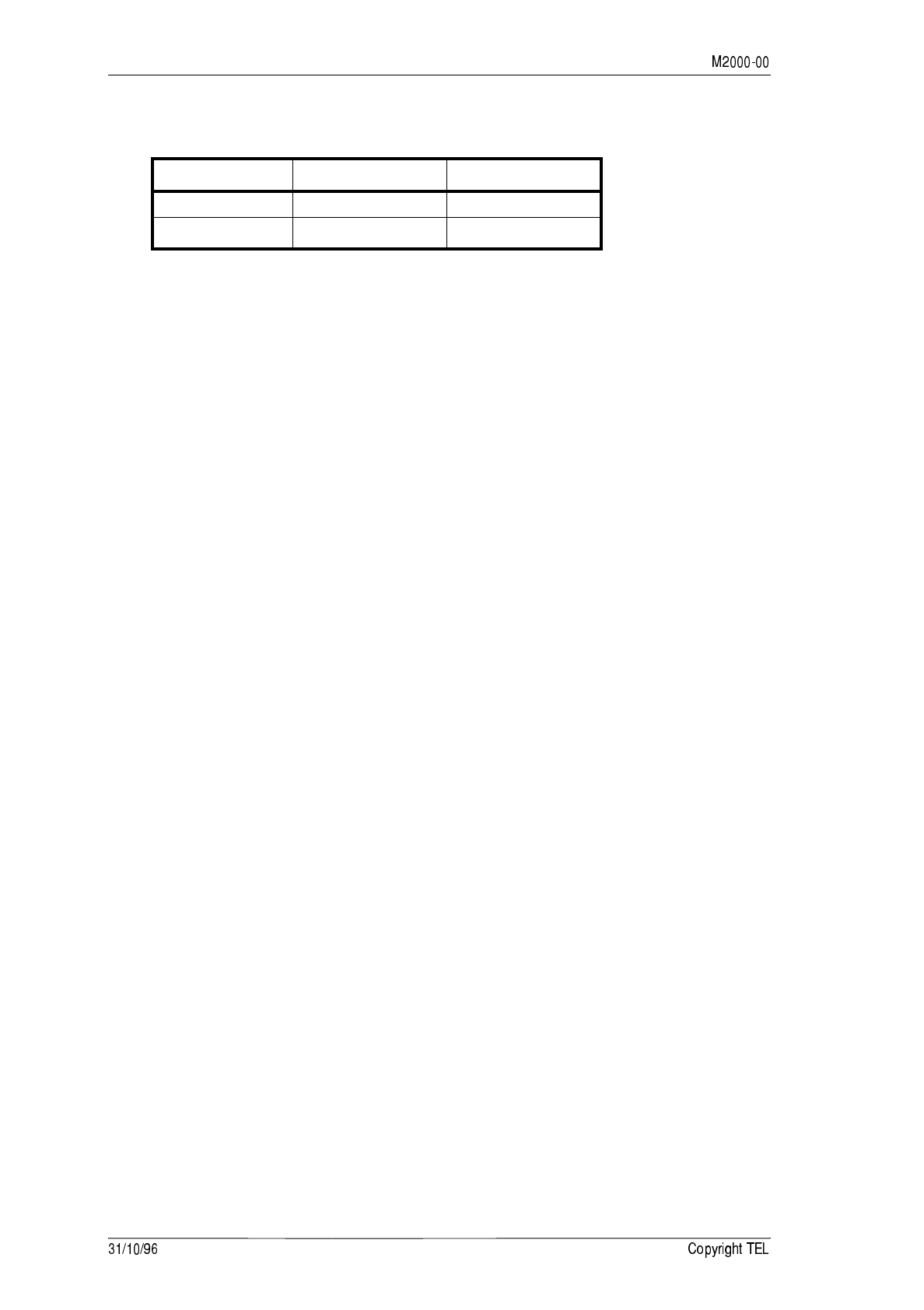
4 Replacement Transistor Fitting
Refer to Figure 8.3.3.
aTin the underside of the replacement transistor PCB.
Place the PCB as shown, and sweat-solder into position, soldering the centre strip
first, followed by the other strips.
T2000-500 T2000-600
*C330 5p6 -
C331 5p6 4p7
*C332 22p 5p6
*C324
Q306
C325
C323
*C329
*C327
Q305
SRF 16
Resistors
TRANSISTOR SUBSTITUTE
C239 C237
T2000-500/600
220-01287-00
0305
d
!"#$%
bSolder the chip capacitors onto the replacement transistor PCB, in the positions
shown. Refer to the table below for capacitor values and the distance ‘d’.
The distance ‘d’ shown in Figure 8.3.3 is measured from the edge of the transis-
tor top cap to the centre of the capacitors.
cSolder the 2 SRF16 resistors in the positions shown. Keep the leads as short as pos-
sible and ensure the resistors do not cause a short circuit.
5Replace the radio type label and type approval certificate number label on the
heatsink fins with the new type label and corresponding type approval certificate
number label.
;4
1Adjust RV324 to set the required output power level.
If the output power is set to 1W for RF control purposes, program the radio for
high power and adjust RV324 for 1W.
2Seal RV324 with permanent adhesive so that the power cannot be readjusted.
Frequency Range:
T2000-500 .. 400 to 470MHz
T2000-600 .. 450 to 520MHz
Supply Voltage .. 0.8 to 16V DC
Power Output .. adjustable 1 to 7W
Temperature Range .. -30°C to +60°C
Stability (power output set to >1W) .. transmitter stable into 5:1 VSWR
(all phase angles)
*d is 13mm if Q305 is a BLW81 transistor
T2000-500 T2000-600
Capacitor Value 22p 18p
Distance (d) 14.5mm*11.5mm
&'()
; )8?
The T2000-05 remote speaker kit provides a 4Ω external speaker for T2010, T2015 and
T2030 models.
!)6(
The T2000-05 kit contains the following components:
.
&
1Choose a suitable mounting position for the speaker.
With the speaker fitted to the mounting bracket, check that it does not interfere
with the operation of any of the vehicle controls.
2Fix the speaker mounting bracket securely in the chosen location with suitable fas-
teners. Two M4 self tapping screws and ‘U’ type captive nuts have been supplied
for this purpose.
Check before drilling that the drill will not damage any components or
wiring behind the panel.
aIf drilling directly into metal, drill two 3.5mm holes in the appropriate locations
and secure the bracket with the supplied M4 self tapping screws.
bIf mounting the bracket to any other material, such as plastic, drill two 4.5mm
holes and attach the bracket with the M4 screws and captive nuts. Slide a captive
nut over the edge of the panel to align with each hole, ensuring that the screw will
pass through the larger hole to thread into the smaller hole.
cIf neither of the above methods is appropriate, M4 screws, nuts and shakeproof
washers are equally suitable.
3Attach the speaker to the mounting bracket with the thumbscrews.
Quantity Description
1 T2000 speaker complete with mounting bracket and thumb screws
2 M4 self tapping screws
2 ‘U’ type captive nuts for self tapping screws
5m speaker wire complete with receptacles and speaker socket
&'()
4Refer to Figure 8.4.1.
Remove the existing internal speaker link and insert the three speaker wire recep-
tacles into the appropriate power connector holes, as shown.
If the internal speaker is not required, cut the internal speaker ground link.
5Plug the speaker into the socket provided on the speaker wire, neatly loop any
excess wire and secure with a cable tie.
Peel the protective plastic off the “Tait” label on the front of the speaker.
Internal speaker link
(T2010, T1015 & T2030:
cut to disable)
Ignition
External
Power supply:
13.8V
Ground
External speaker:
Ground
Liv
e
{
Not normally
fitted

!(*+)
;*78'$?
(
The T2000-06 desktop microphone has an internal omni-directional dynamic element,
pre-amplifier and compressor loop. The microphone output is adjustable by a potenti-
ometer (R11) which is accessible through a hole in the bottom of the case.
The desktop microphone has a switch provided for hookswitch monitoring, which can
be locked if required.
.
&
The T2000-06 has grommets for both Series I and II radios fitted to the microphone cord.
1Remove the Series I grommet from the microphone cord.
2Fit the desktop microphone lead to the T2000 control head microphone socket,
then push the grommet in place.
;*;4
Both the desktop microphone and the T2000 radio have an internal compressor and it is
advisable that the T2000 compressor be disabled to avoid the possibility of ‘hunting’.
This can be done either by disabling the T2000 compressor or by adjusting the output
level at the desktop microphone.
'$(
1Disable the internal T2000 compressor by solder shorting the pads labelled ‘ALC
disable’ on the logic PCB.
2Observe the waveform at TP606 with an oscilloscope, and whistle into the micro-
phone at close range.
Adjust the output level of the microphone until the waveform is just below clip-
ping.
'$(
1Leave the T2000 internal compressor enabled.
2Set the transmitter average deviation by whistling into the microphone at the
required distance from the microphone.

!(*+)
3Adjust the output level at the microphone to approximately 80% deviation
(±4kHz for wide band or ±2kHz for narrow band).
,
Under some conditions, the microphone may pick up excessive background noise. In
this situation, the output can be reduced using either of the procedures described
below:
1Change the value of R12 from 10kΩ to 47kΩ (refer to the circuit diagram). This
will result in a 10dB output reduction.
2Fit a 2K2 pot parallel with the microphone element.
Adjust the output level to suit.
!(*+)

!(*+)

#*,*+) *
* ;+7'.'$?
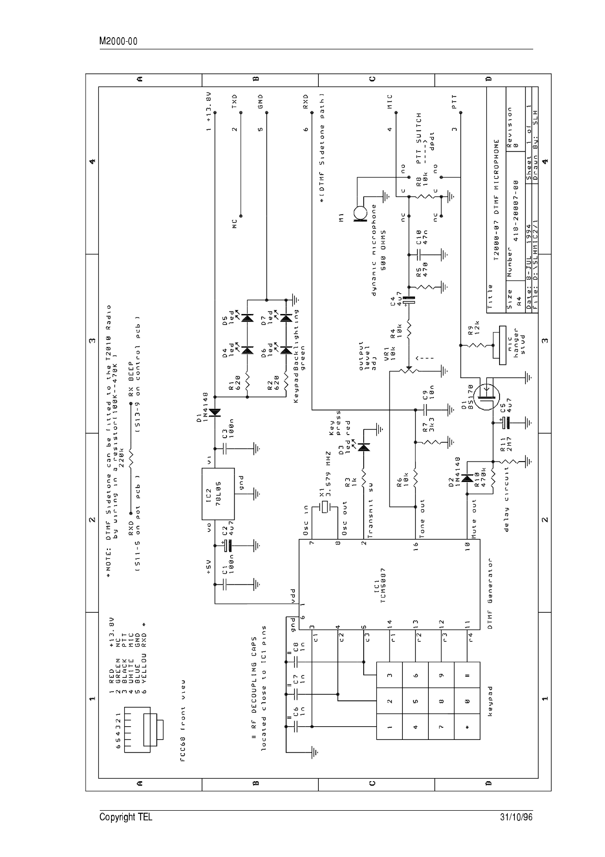
The T2000-07 DTMF microphone has an omni-directional dynamic element and internal
DTMF tone generator. The DTMF tone level is adjustable by an internal potentiometer
(VR1) which is accessible when the rear case is removed.
The DTMF microphone is intended for use with all T2000 Series II radios.
* .
&
The T2000-07 has grommets for both Series I and II radios fitted to the microphone cord.
1Remove the Series I grommet from the microphone cord.
2Fit the DTMF microphone lead to the T2000 control head microphone socket, then
push the grommet in place.
*
1The microphone LED is used to indicate ‘key pressed’. The LED is on for normal
operation and is off when a DTMF key is pressed.
2The PTT switch changes the microphone input to the radio from DTMF tone to the
dynamic microphone. This is to prevent the microphone signals distorting the
DTMF tones.
3The operation of a DTMF key automatically operates the transmitter PTT and
holds it on for a short time after the release of the DTMF key. This is to hold the
transmitter on during interdigital pauses.
* ;+;4
Remove the microphone back cover and set the DTMF tone level to approximately
80% deviation (±4kHz for wide band or ±2kHz for narrow band).
7'.(0< 2
The DTMF tone output is also fed into the receive data line and can be used to provide a
sidetone.
1Refer to the diagram on the following page.
Solder a resistor to S13 pin 9 (RX-BEEP) on the bottom side of the T2010 control
PCB.
* #*,*+)
The value of the resistor adjusts the sidetone level and is between 100kΩ and
470kΩ, typically 220kΩ.
2Slide a length of silicone sleeving over the resistor, and connect a wire between the
resistor and S11 pin 5 (RXD) on the pot PCB, as shown.
TP606
TP605
TP603
TP602
TP601
DISABLE
ALC
FUSE
S13 pin 9
Connect to
S11 pin 5
#*,*+) *

* #*,*+)
-.) +
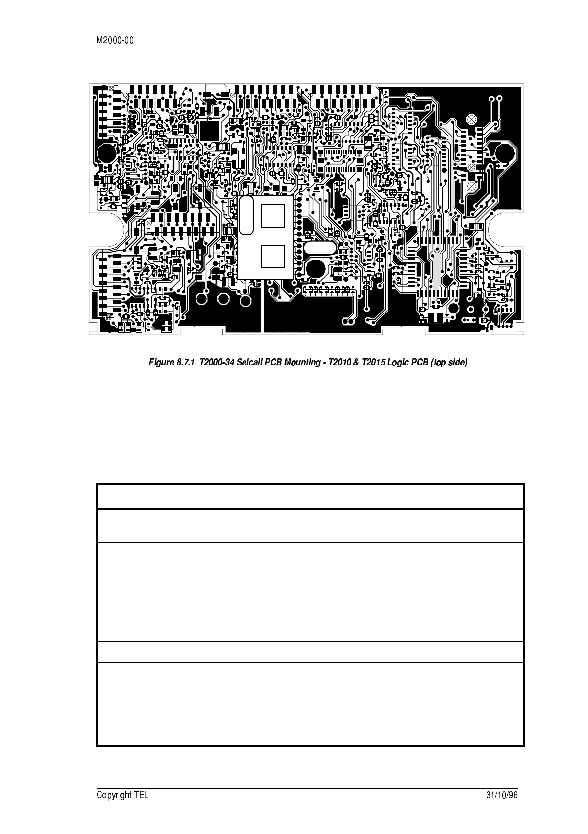
+ ;?
The T2000-34 kit provides selective tone calling (Selcall) facilities for T2010 and T2015
model T2000 Series II radios.
The Selcall kit consists of a small module and a 5MHz crystal that are fitted to the
radio’s logic PCB. This option allows selective individual or group calls within a fleet of
radios, on channels that have Selcall programmed. Selcall parameters and features are
set up and enabled during programming. Both Sigtec and International group formats
are supported by the T2000-34 PCB.
Refer to Section 8.7.3, “Programming” for a list of user-selected features. The following
topics are covered in this Section:
Section Title Page
8.7.1 Components Required 8.7.2
8.7.2 Fitting 8.7.2
8.7.3 Programming 8.7.3
+ -.)
+ !)6(
The T2000-34 kit contains the following components:
+ .
&
Refer to Figure 8.7.1 and Section 7.10, “T2010 & T2015 HC05 Logic PCB”.
1Remove the top cover of the radio by unscrewing the four cover screws, unscrew
the logic PCB and fold-out.
2Unplug the connecting looms, if required.
3Place the Selcall module flat on the logic PCB, as shown in Figure 8.7.1, with the
component side facing upwards.
Solder the leads on the bottom side of the PCB and trim as necessary.
4Fit the supplied 5MHz crystal flat on the PCB in location ‘#X502’ as follows:
Peel the protective backing off the self-adhesive foam tape on the underside of the
crystal.
Insert the crystal leads into the holes provided and press the crystal down onto
the PCB.
Solder the leads on the underside of the PCB and trim as necessary.
5Reconnect any looms that were unplugged in step 2.
Refit the logic PCB to the radio and secure with the three retaining screws.
Refit the top cover and secure with the four retaining screws.
Quantity Description
1 T2000-34 Selcall module
1 5MHz crystal with insulator
-.) +
+
&
&
The radio must now be reprogrammed to set the various Selcall parameters listed in the
following table. Refer to the manual supplied with the T2000-20 programming kit for
details.
Parameter Selection
Tone Set CCIR, EIA, EEA, ZVEI-1, ZVEI-2, ZVEI-3, DZVEI,
PZVEI
Tone Frequencies 16 tones corresponding to the International Standard
for the selected tone set, plus ‘no tone’
Tone Period 20*, 33, 40, 50*, 60*, 70 & 100ms
Lead-In Delay between 0 & 5100ms in 20ms steps
Lead-In Tone any of the 16 valid tones, or ‘no tone’
Decode Sequence individual or group decode
Encode preset
Group Decode Format Sigtec or International
Auto Acknowledge enabled or disabled
Group Dialling enabled or disabled
X501
SK505
S8
S3
S2
S15
S14
S13
S1
RV507
R727
R726
R725
R724
R721
R720
R708
R707
R706
R705
R704
R703
R702
R701
R700
R699
R698
R697
R696
R695
R694
R693
R692
R691
R690
R689
R688
R687
R686
R685
R684
R683
R682
R681
R680
R679
R678
R677
R676
R675
R674
R673
R672
R671
R670
R669
R668
R667
R666
R665
R664
R663
R662
R661
R660
R659
R658
R657
R656
R655
R654
R653
R652
R651
R650
R649
R648
R647
R646
R645
R644
R643
R642
R641
R640
R639
R638
R637
R636
R635
R634
R633
R632
R631
R630
R629
R628
R627
R626
R625
R624
R623
R622
R621
R620
R619
R618
R617
R616
R615
R614
R613
R612
R611
R610
R609
R608
R607
R606
R605
R604
R603
R602
R601
R600
R599
R595
R593
R592
R586
R585
R584
R583
R582
R581
R580
R579
R578
R575
R574
R572
R571
R570
R569
R568
R547
R546
R544
R543
R542
R541
R540
R539
R538
R537
R536
R535
R534
R533
R532
R531
R530
R529
R528
R527
R526
R525
R524
R523
R522
R521
R520
R519
R518
R516
R515
R514
R513
R512
R511
R510
R509
R508
R507
R506
R505
R504
R503
R502
R501
Q608
Q607
Q606
Q605
Q604
Q603
Q602
Q601
Q520
Q510
Q509Q508
Q507
Q506
Q505
Q504
Q503
Q502
Q501
L501
IC614
IC604
IC603
IC602
IC601
IC513
IC511
IC509
IC507
IC506
IC504
IC501
D500
C705
C702
C651
C650
C648
C647
C646
C645
C644
C643
C642
C641
C640
C639
C638
C637
C636
C635
C634
C633
C632
C630
C629
C628
C627
C626
C625
C624
C623
C622
C621
C620
C619
C618
C617
C616
C615
C614
C613
C612
C611
C610
C609
C608
C607
C606
C605
C604
C603
C602
C601
C600
C547
C546
C545
C544
C543
C542
C541
C540
C530
C529
C528
C527
C526
C525
C524
C522
C521
C520
C519
C518
C517
C515
C514
C509
C507 C506
C505
C504
C503
C502
C501A
C501
C500
#X502
#SPEC9
#SPEC8
#SPEC7
#SPEC6
#SPEC5
#SPEC4
#SPEC3
#SPEC2
#SPEC10
#SPEC1
#RV508
#R723
#R722
#R714A
#R714
#R713
#R712
#R711
#R710
#R651
#R596
#R595
#Q508
#IC512
#IC510
#C704
#C703
#C701
#C700
#C631
#C630
P2
P1
#X502
T2000-34

+ -.)
* These tone periods are not defined by international standards. Wherever possible,
use the international standard tone periods.
Deferred Calling enabled or disabled
ANI Sequence leading, trailing or random encoding
Emergency Sequence enabled or disabled
Alert internal and external durations
Tone Blanking standard
Parameter Selection
-!)
;*?
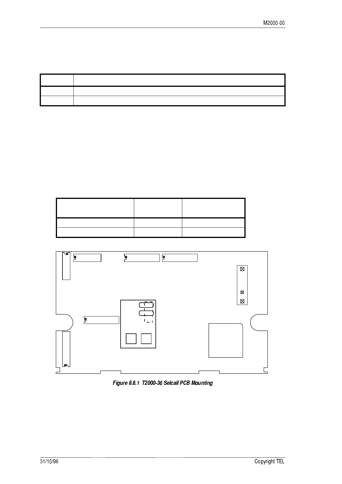
The T2000-36 Selcall PCB plugs into an options connector on the top side of the logic
PCB, and provides selective tone calling (Selcall) facilities for T2010,T2015, T2020 or
T2050 model T2000 Series II radios.
This option allows selective individual or group calls within a fleet of radios, on chan-
nels that have Selcall programmed. Selcall parameters and features are set up and ena-
bled during programming. Both Sigtec and International group formats are supported
by the T2000-36 PCB.
The following topics are covered in this Section:
Section Title Page
8.8.1 Components Required 8.8.2
8.8.2 Fitting 8.8.2
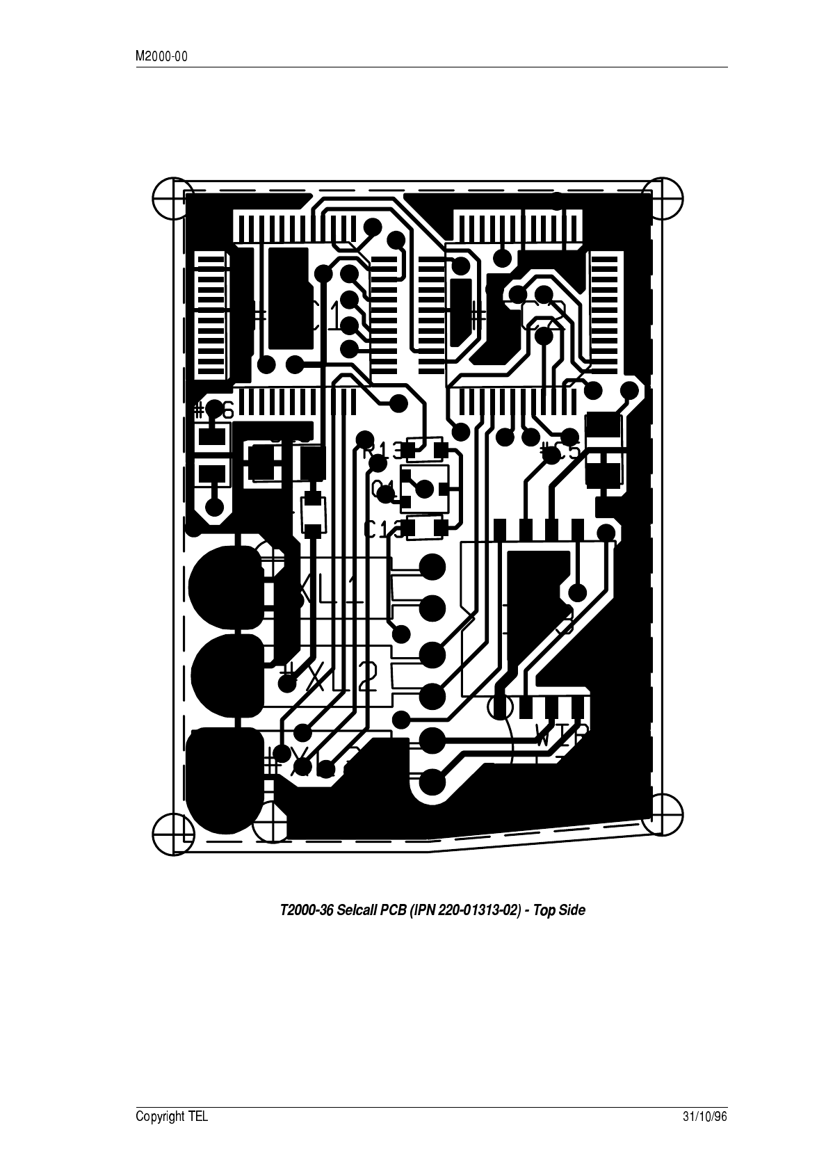
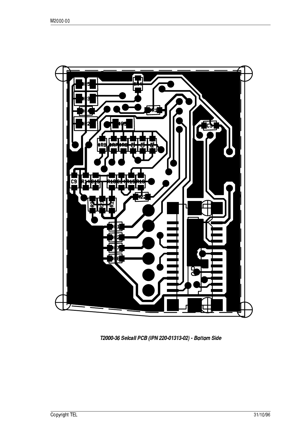
8.8.3 PCB Information 8.8.4
-!)
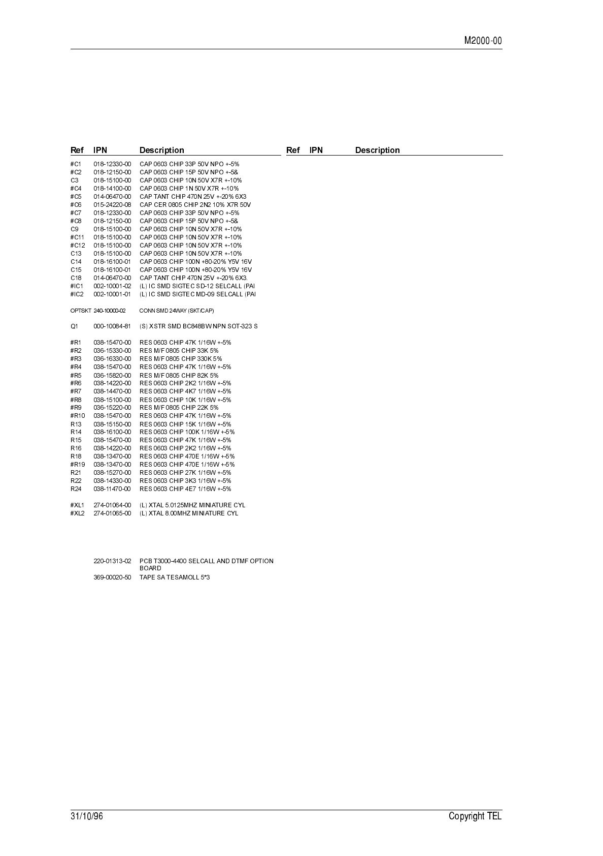
!)6(
The T2000-36 Selcall kit contains the following components:
.
&
1Refer to Figure 8.8.1.
Remove the top cover of the radio by unscrewing the four cover screws, unscrew
the logic PCB and fold-out.
Position the T2000-36 PCB as shown, and plug into the connector on the T2000
logic PCB:
Quantity Description
1 T2000-36 PCB assembly
12mm PVC foam tape
Model PCB IPN Connector Circuit
Reference
T2010 & T2015 220-01377-01 P1
T2020 & T2050 220-01344-02 #T3K44
SK505
S8
S3
S2
S15
S14
S13
S1
P2
P1
T2000-36
P1
T2000-36

-!)
2Position the foam tape provided on top of XL2, on the T2000-36 Selcall PCB.
3Carefully fold the logic PCB back in position and secure using the three logic PCB
retaining screws.
Refit the top cover.
4Refer to the T2000 Programming Software User’s Manual (IPN 439-22000-02, or
later) for set-up information.
;*#0:;;2
-!)
!/
'$<'
-!)
-!) *
-!) +

-!)
.*,) -
- ;7'.?
The T2000-40 DTMF kit provides DTMF dialling facilities for T2020 model T2000 Series
II radios. It consists of a small module which is fitted to the control head PCB. Once
installed, all parameters (such as tone durations and hold times) can be programmed as
required.
- .
&
1Remove the four screws from the back of the control head and remove the back
cover, taking care not to lose the captive nuts.
Unplug the connecting loom from the control head PCB, if required.
2Refer to the diagram below.
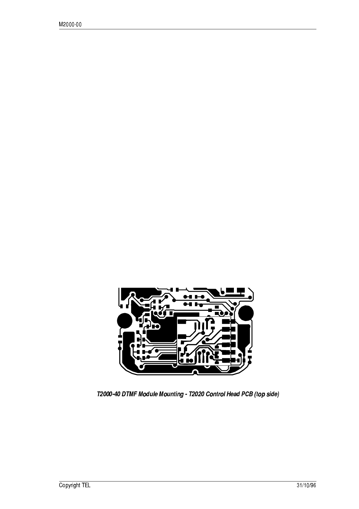
Place the DTMF module flat on the control head PCB in location ‘S20’ with the
component side facing upwards.
Solder in place, checking that each pin is correctly positioned over the appropriate
pad.
3Reconnect the loom (if plugged in step 1), refit the loom cable into the cable
restraint in the back cover, and screw the cover back into place.
Ensure that the captive nuts are correctly located in the back cover before fitting.
-
&
&
The radio must now be programmed with the various DTMF parameters. Refer to the
manual supplied with the T2000-20 programming kit for details.
T2000-40

- .*,)
./ '0)
; @!!<3?
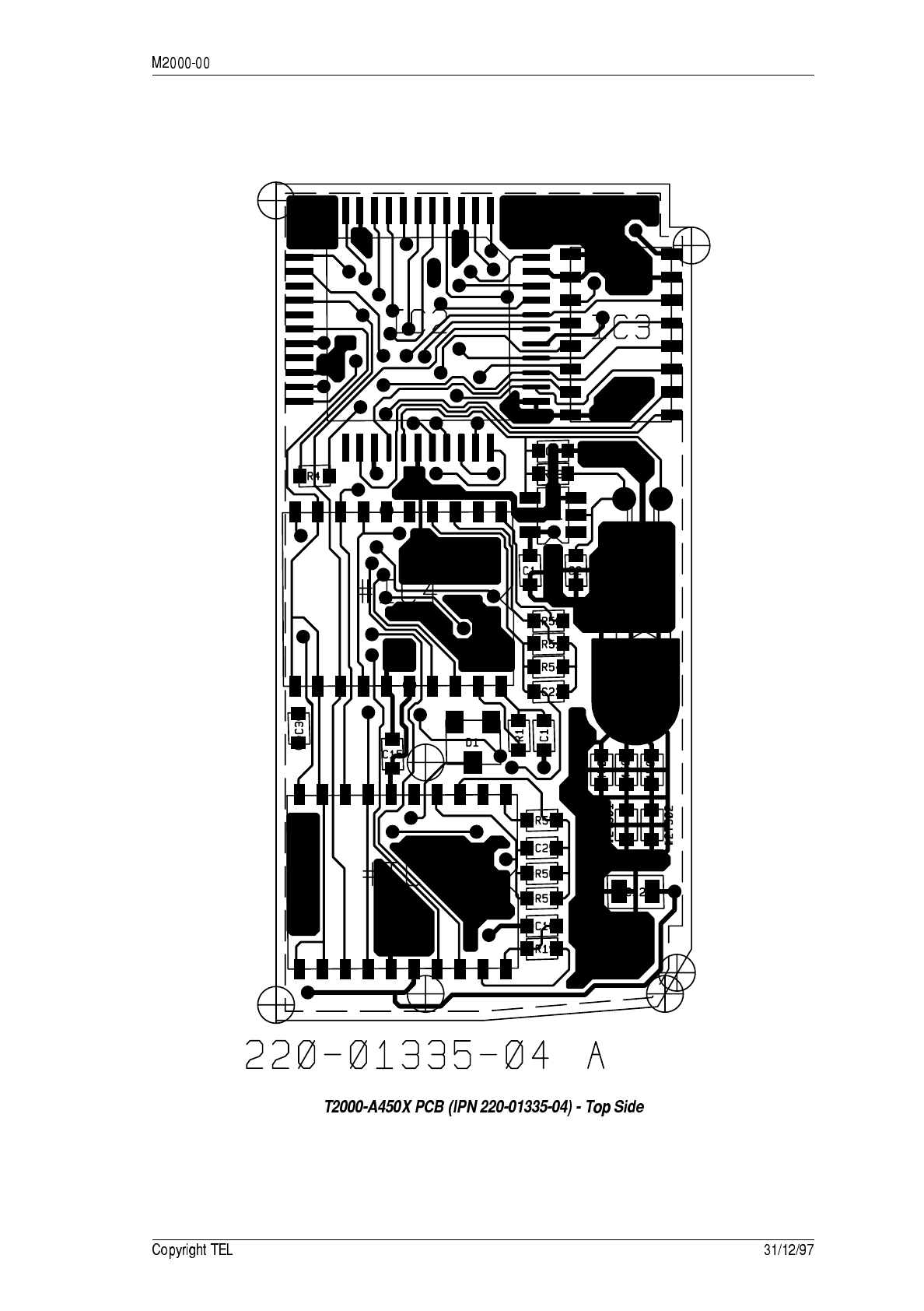
The T2000-A450X CTCSS and scrambler PCB plugs into an options connector on the top
side of the T2000 Series II logic PCB, and can be configured in two ways:
The CTCSS option is used in trunked radios, and has 38 independent receive and trans-
mit tones, set by solder links on the T2000-A450X PCB.
The scrambler option can be used in either trunked or conventional radios, and is ena-
bled/disabled by the auxiliary ( ) key (conventional models) or function ( )
key (trunked models). The scrambler uses a simple frequency inversion algorithm that
prevents casual eavesdropping by other radio users. After descrambling, the recovered
speech suffers from some degradation in clarity.
The T2000-A4500 CTCSS kit is only compatible with the following radio and
PGM software versions:
The following topics are covered in this Section:
Product Code Option T201X T2020 T203X T2040 T2050
T2000-A4500 CTCSS xx x
T2000-A4502 Scrambler
Radio Radio Software
Version PGM Software
Version
T2030 3.24 or later later than 1.44
T2035 3.28 or later
T2040 5.36 or later later than 2.57
Section Title Page
8.10.1 Components Required 8.10.2
8.10.2 Fitting 8.10.2
8.10.3 T2000-A450X Link Options 8.10.3
8.10.4 PCB Information 8.10.5
Fn
./ '0)
!)6(
The T2000-A450X kits contain the following components:
.
&
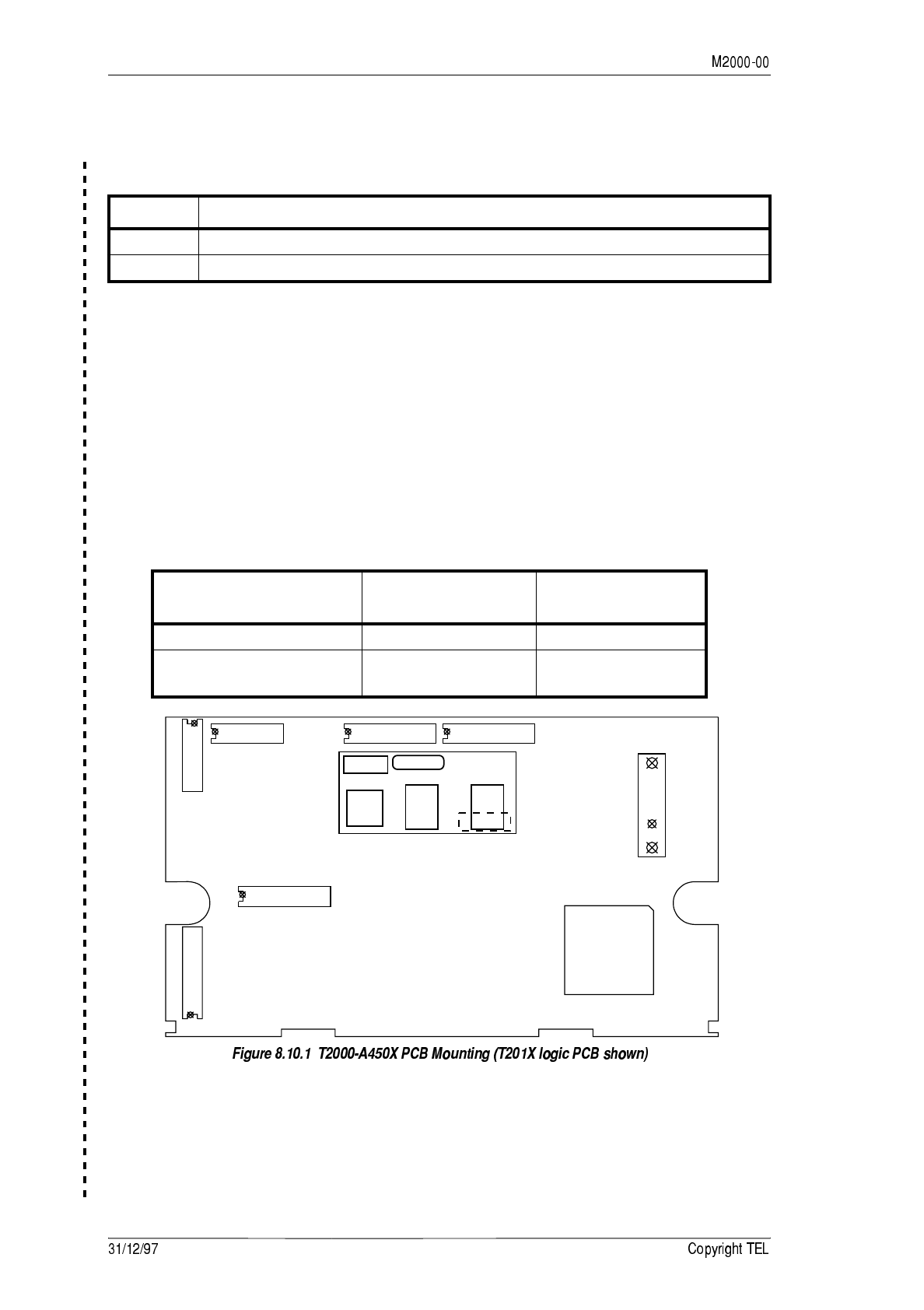
1Refer to Figure 8.10.1.
Remove the top cover of the radio by unscrewing the four cover screws, unscrew
the logic PCB and fold out.
2Select the T2000-A450X link options, as described in Section 8.10.3, “T2000-A450X
Link Options”.
Position the T2000-A450X PCB as shown, and plug into the connector on the
T2000 logic PCB:
2Position the foam tape provided on top of #IC5, on the T2000-A450X PCB.
3Carefully fold the logic PCB back in position and secure using the three logic PCB
retaining screws.
Refit the top cover.
Quantity Description
1 T2000-A450X PCB assembly
12mm PVC foam tape
Model PCB IPN Connector Circuit
Reference
T2010 & T2015 220-01377-01 or later P2
T2020, T203X, T2040 &
T2050 220-01344-02 or later #T3K45
SK505
S8
S3
S2
S15
S14
S13
S1
P2
P1
T2000-45
P2
./ '0)
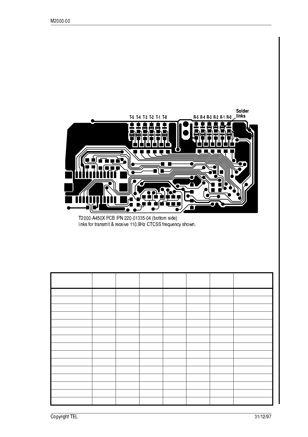
; @#8
There are 2 groups of links on the underside of the T2000-A4500 PCB, the receive
(R) group and the transmit (T) group. Each group contains 6 bits that are pulled
logic high or low, by either solder links or zero ohm resistors.
The receive settings are set by links R-0 to R-5 and the transmit settings by links T-
0 to T-5. A short to the 5V line represents a ‘1’, and a short to ground represents a
‘0’.
The following diagram shows the T2000-A450X PCB, with links indicated.
; !!!/#8
The following table gives the linking details for the 38 independent transmit and receive
CTCSS frequencies.
Tone Number R-5
T-5 R-4
T-4 R-3
T-3 R-2
T-2 R-1
T-1 R-0
T-0 CTCSS
Frequency (Hz)
1 000000 67
2 000001 71.9
3 000010 74.4
4 000011 77
5 000100 79.7
6 000101 82.5
7 000110 85.4
8 000111 88.5
9 001000 91.5
10 001001 94.8
11 001010 97.4
12 001011 100
13 001100 103.5
14 001101 107.2
15 001110 110.9
./ '0)
; 3!/#8
The T2000-A4502 has the following R settings linked during manufacture. The T
settings have no effect.
16 001111 114.8
17 010000 118.8
18 010001 123
19 010010 127.3
20 010011 131.8
21 010100 136.5
22 010101 141.3
23 010110 146.2
24 010111 151.4
25 011000 156.7
26 011001 162.2
27 011010 167.9
28 011011 173.8
29 011100 179.9
3 0 011101 186.2
31 011110 192 .8
32 011111 203.5
33 100000 210.7
34 100001 218.1
35 100010 225. 7
36 100011 233.6
37 100100 241.8
3 8 100101 250.3
R-5 R-4 R-3 R-2 R-1 R-0
111111
Tone Number R-5
T-5 R-4
T-4 R-3
T-3 R-2
T-2 R-1
T-1 R-0
T-0 CTCSS
Frequency (Hz)
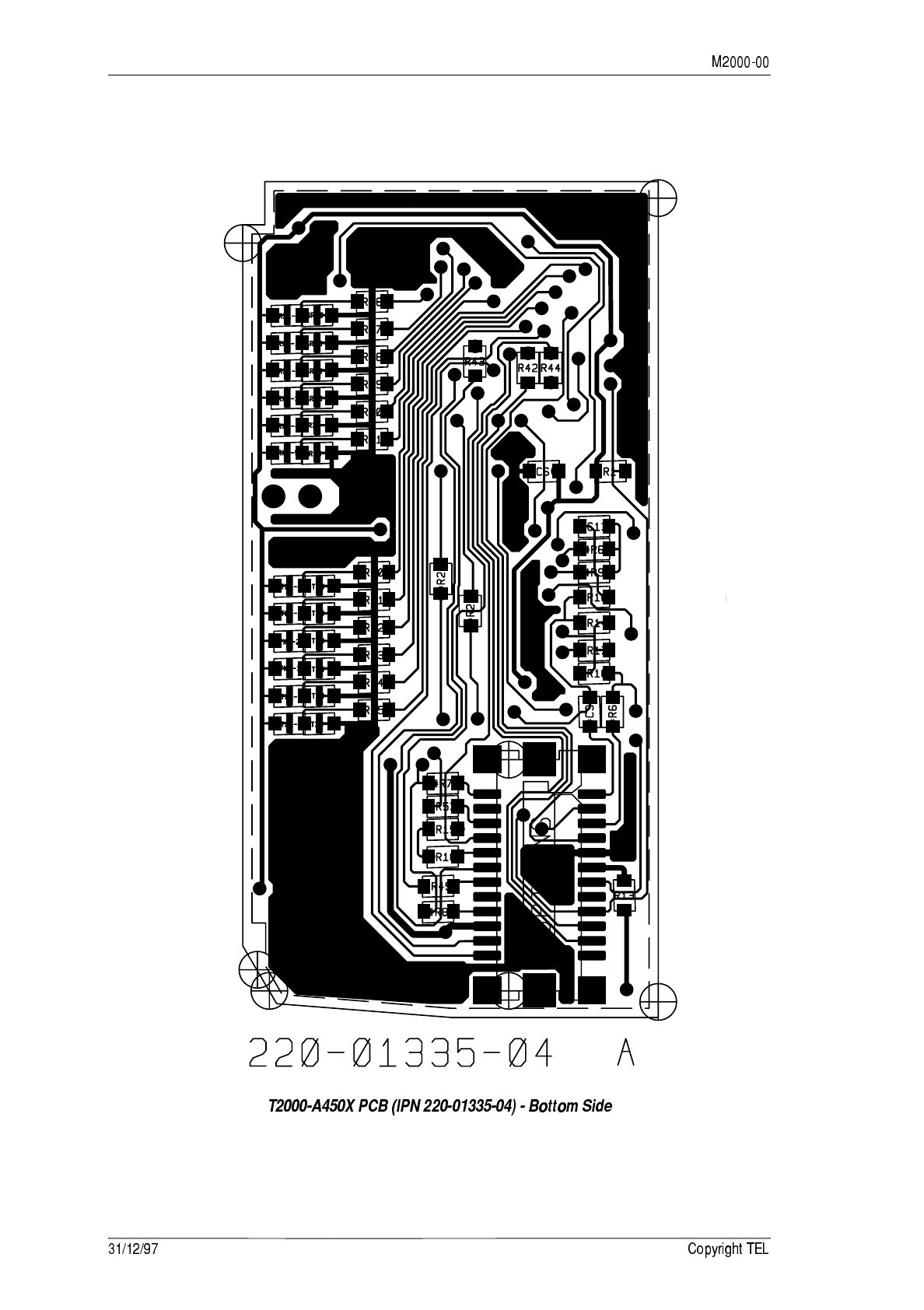
; @#0:; ;2
./ '0)
!/

* ./ '0)
./ '0) +
./ '0)
./ '0) -
./ '0)
123)
; >(?
The T2000-50 handsfree kit is designed for use with all T2000 Series II mobiles, and
allows communication through the normal PTT microphone, or ‘handsfree’ operation
through a directional microphone.
When ‘handsfree’ operation is being used, the transmitter is activated either by the foot-
switch (Manually Operated Transmit) or automatically, by detecting the sound of a
voice. The latter is known as the Voice Operated Transmit (VOX) mode. VOX operation
is only intended for use in quiet modern vehicles.
With trunked radios, a call needs to be established before VOX or footswitch
becomes operative. Normal handsfree operation can be used on a conventional
channel.
The following topics are covered in this Section:
Section Title Page
8.11.1 Components Required 8.11.2
8.11.2 Fitting 8.11.2
8.11.3 Fitting The Complete Unit In The Vehicle 8.11.3
8.11.4 T2000-50 Set-Up 8.11.5
8.11.5 Signal Specifications 8.11.7
8.11.6 Specifications 8.11.8
8.11.7 Circuit Description 8.11.8
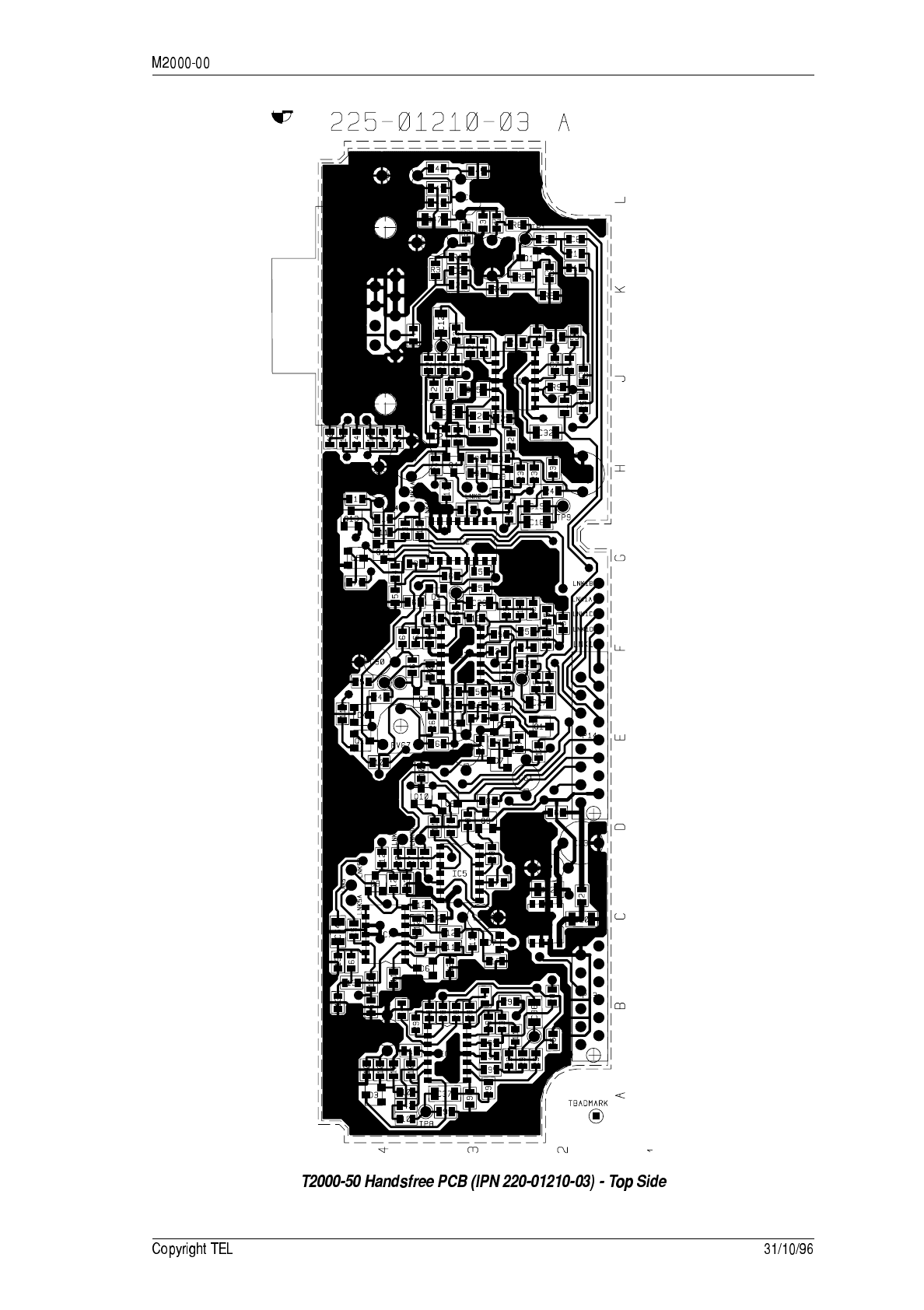
8.11.8 PCB Information 8.11.10
123)
!)6(
The T2000-50 kit contains the following components:
.
&
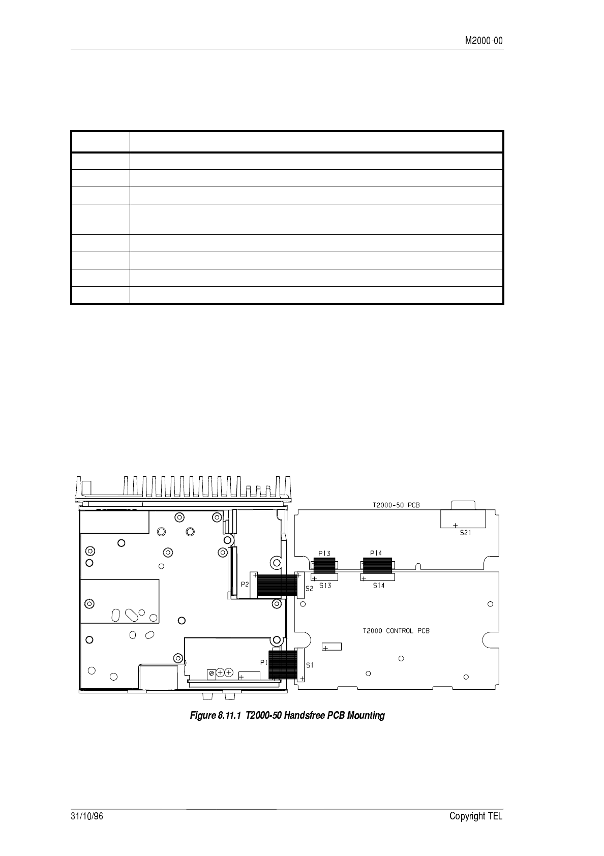
1Refer to Figure 8.11.1.
Remove the top cover of the radio by unscrewing the four cover screws, unclip the
D-range blanking plate in the rear of the T2000 radio, unscrew the logic PCB and
fold-out.
Position the T2000-50 PCB as shown, and connect the Micromatch connectors P13
and P14 to S13 and S14 on the T2000 logic PCB.
2 T2010 & T2015: Remove R513 (0Ω resistor) on the logic PCB.
Quantity Description
1 T2000-50 PCB assembly
1 directional microphone (with optional sunvisor clip or tie clip)
1 footswitch
19 way D-range assembly with 2 in-line connectors & microphone socket
attached
1 shroud (alternative shroud - not required for T2000 Series II radios)
1 2 way in-line connector
3 M3x8 pan Pozi Taptite screws
2 4-40x¼ pan Pozi Taptite screws (black)

123)
3After manufacture, the T2000-50 PCB links are left open and will need to be cus-
tomer selected. For details of optional links, refer to the Link Options Table in the
circuit diagram.
Non-trunked radios: standard links are 4B and 5A.
4Set up the T2000-50, as described in Section 8.11.4, “T2000-50 Set-Up”.
A +5V logic signal is provided to indicate VOX activity (S21 pin 7). ‘VOX’ (violet
wire) and ‘ground’ (grey wire) are both available from the D-range assembly red
in-line connector.
A spare in-line connector is also included in the kit for interfacing to an appropri-
ate visual indicator e.g. an LED.
5Carefully fold the logic and T2000-50 PCBs back in position, guiding the D-range
connector through the hole provided in the T2000 chassis.
Check that no electrolytic capacitors are touching the T2000 chassis (e.g. C21 or
C51.)
6Secure using the three logic PCB retaining screws and the three M3x8 screws pro-
vided and refit the top cover.
Plug the D-range assembly provided in the kit into the D-range connector (S21).
Holes are provided in the T2000 chassis for the D-range plug locking screws.
Use the two black 4-40x¼ Taptite screws provided in the kit to form the threads.
.
&
$!4$%$
'$'
&
The handsfree directional microphone plugs into the T2000 via the D-range assembly
microphone socket. The positioning of the microphone is important for correct opera-
tion of the handsfree unit and some experimentation may be necessary to obtain the best
performance from the VOX.
• The microphone should be mounted in a position 20cm or less from the driver.
• The microphone location should be free from vibration.
• The microphone must face the driver.
.$'
&
The footswitch plugs into the D-range interface via the black 2 way in-line connector. It
is recommended that the footswitch be screwed to the floor.
The 3m lengths of the footswitch and microphone can be effectively extended
by fitting a standard 9 way D-range extender cable between the radio and the
D-range assembly. These extension cables are not included as standard but are
available from most computer outlets.

123)
)(
&
&
The radio may need reprogramming to accommodate the handsfree unit. The
key for the T2010, T2015 and T2020 or the key for trunked radios
must be programmed for latching if VOX mode is to be used. Refer to the T2000 pro-
gramming manual.
For T203X and T2040 radios, the ‘handsfree’ option will also need to be selected under
‘Specifications’ (refer to the ‘Specifications’ section of the programming manual).
%=,
Although the VOX circuitry has been designed to operate in varying conditions, it may
be necessary to change the minimum threshold for VOX operation.
Monitor TP5 without the directional microphone connected and adjust RV67. Turning
RV67 clockwise increases sensitivity, and anticlockwise decreases sensitivity.
For the majority of applications, it is recommended that the setting is left at the
factory setting of 0.8V.
Fn
123)
; ;4
56)6(
T2000-50 set-up should only be necessary after major repair.
• AF signal generator
• modulation analyser
• high impedance voltmeter (e.g. VTVM)
• oscilloscope
• power supply (+13.8V)
• RF power meter or load
• 30dB RF attenuator
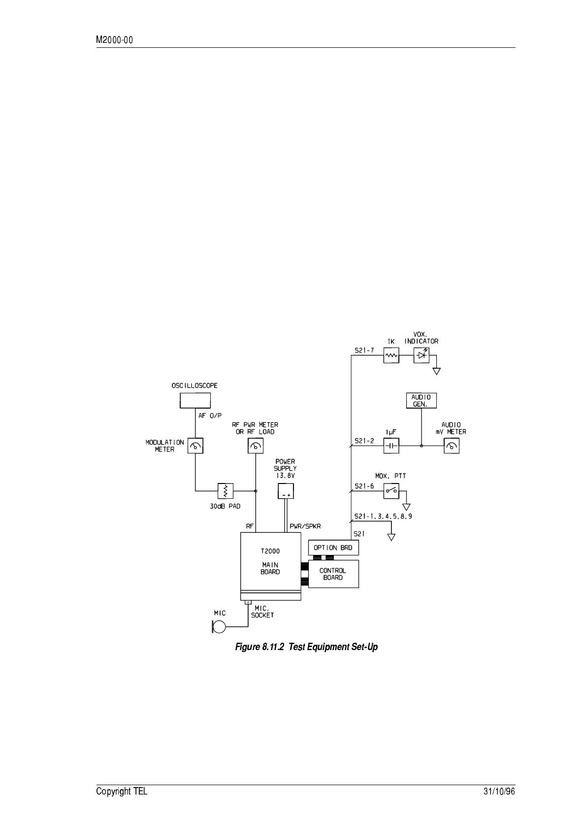
The following diagram shows a typical test set-up.
1Set up the equipment as shown in Figure 8.11.2, and set the audio generator to
1kHz at a level of 0.8mV.
Switch on the T2000 and check the increase in current with the T2000-50 fitted is
less than 30mA.
* 123)
2Switch on the MOX (Manually Operated Transmit) PTT and check that the modu-
lation is at approximately 60% of full system deviation. Check that no audio path
is evident through the normal microphone.
Activate the PTT on the normal microphone and check that there is now an audio
path through the microphone.
3With no audio, adjust RV67 for 0.8V at TP5.
Remove the TCXO PCB to operate the /IN-LOCK signal and check that the DC
level now goes to 6.5V ±0.5V. Replace the TCXO.
4Increase the audio level by 10dB.
With all PTTs off, activate the or keys (radio is in VOX
mode).
Sweep the audio generator slowly from 1kHz to 100Hz and back again and check
that the transmitter keys between 700Hz ±70Hz and 250Hz ±25Hz.
When going from receive to transmit the radio should key instantly at these cut-
offs. When going from transmit to receive check there is a delay of approximately
1.5 seconds.
Check that VOX transmit is inhibited if the channel is busy (assuming LINK4B is
fitted).
5Switch on the MOX PTT and set the audio generator to 1kHz at a level of -50dBm
(3mV).
Monitor TP9 and check that the level on the scope is 1.2Vp-p ±0.2V.
Increase the audio level by 10dB and check that the level on the scope is about the
same.
Decrease audio level by 20dB. After observing the charging action of the compres-
sor, the level on the scope should be 0.4Vp-p ±0.1V.
Trunking only: The audio at TP9 should be there on an assigned channel, a
non-trunked channel or in test mode. When the radio is on a control channel or
hunting for a control channel, the audio should be muted.
6A final system check can be done with the directional microphone and footswitch.
Fn
123) +
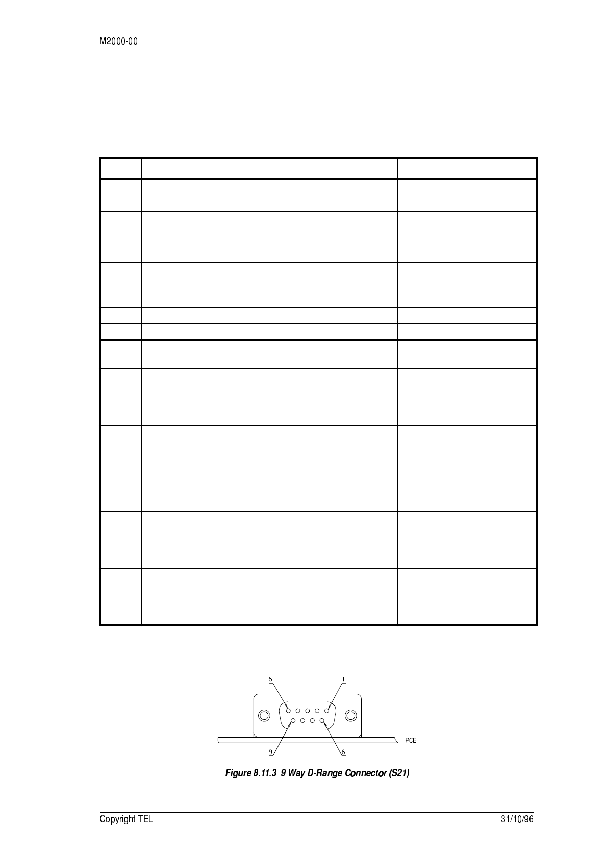
&
The following table describes S21 pin-outs, and relevant interface signals on S13 and S14
(T2000 logic PCB). S21 is the 9 way D-type connector mounted on the heatsink at the
rear of the radio.
The following diagram shows the pin designations of S21, viewed from the rear of the
radio.
Pin No. Signal Description Level
S21-1 GND
S21-2 MIC Input for directional mic. audio
S21-3 GND
S21-4 GND
S21-5 GND
S21-6 FT-SWTCH Requests handsfree transmit.
S21-7 VOX Output signalling valid VOX opera-
tion.
S21-8 GND
S21-9 GND
S13-6 TX-LINE-IN Electret microphone audio switched
in during handsfree transmit. 300mVp-p at 60% mod. 1kHz
S13-7 RX-GTD-AF Used to provide VOX trunking
inhibit for received speech. 110mVrms at 60% mod. 1kHz
S13-11 OPTIONS-GND Provides the ground for the options
circuitry.
S14-1 +13.8V Powers the +8V regulator used to
supply audio circuitry 10.8V to 16V DC
available current 200mA
S14-2 +5V Used to supply power for the logic
circuitry. available current 150mA
S14-3 BUSY Used to mute invalid audio when
transmitter has been inhibited. carrier detect 0V = busy
S14-5 /PTT-TO-OPT Echoed to S14-6 for normal PTT
request. Switches off S13-6. 5V pull-up 0V = Tx
S14-6 /PTT-FRM-OPT Provides the signal for the radio to
transmit. 5V CMOS 0V = Tx
S14-7 /IN-LOCK Used to inhibit VOX Tx requests
when the radio is out of lock. synthesiser lock detect 0V =
lock (lock-up time <20ms)
S14-11 CALL-SW Used by trunking software to mute
invalid audio. 5V CMOS 5V = mute

123)
*
Current .. <30mA
Operating Temperature Range .. -30 to +60°C ambient
Audio:
Input For 60% Deviation .. 1mVrms ± 0.1mV (1kHz, 600Ω)
Microphone .. uni-directional electret
Microphone sensitivity .. -67dB ±3db (0dB = 1V/µbar)
Distortion .. <5%
Delay From Audio To PTT Request .. 20ms (typical)
+ !7
Audio is fed into the preamplifier circuitry (Q1) from the electret microphone via pin 2
of the 9 way D-range (S21). The pre-amplified audio is then split and goes into the
speech bandpass filter and the noise filter.
The speech bandpass filter consists of a 4th order 250Hz high pass filter (IC1) and a gain
stage (IC1) with a 3kHz rolloff. Audio then goes into the compressor circuitry (IC1).
When PTT is requested by the logic circuitry, IC2 switches and the audio is driven into
the TX-LINE-IN at a low impedance. After the high pass filter, audio is tapped off into
the speech VOX filter (IC4), which provides a low pass cutoff of 700Hz. This, combined
with the previous high pass filter, gives the speech VOX filter cutoffs of 250Hz and
700Hz.
The second path of the audio after the preamplifier is to the noise filter (IC3). This con-
sists of a 2nd order high pass filter below 100Hz.
After the gain adjusting stages (IC3 & IC4) each filter goes into a precision rectifier (IC3
& IC4), where their appropriate DC level is presented to a comparator (IC3 pins 12, 13 &
14). The negative input has a potentiometer (RV67) providing a DC offset, which is used
to provide a minimum VOX threshold. This minimum threshold decreases with VOX
activity to provide some hysteresis. The negative input is also held high via IC2, pre-
venting the comparator switching until the synthesiser lock detect line (IN/LOCK) is
low. The positive input has a zener diode to prevent VOX activating when both inputs
are in saturation.
The switching circuitry after the comparator output has a slow decay provided by R69
and C31. IC5 will only allow a VOX PTT request if the AUX line has been taken high.
Two NAND gates in IC5 allow a handsfree PTT request (VOX or MOX) to proceed
unless the PTT-IN line has been taken low. A valid handsfree PTT request will mute the
ordinary microphone and switch IC2, whereas a PTT-IN signal will be mirrored on the
PTT line, without switching in the handsfree audio or muting the ordinary microphone.
The CALL line is used by trunking software to mute the handsfree audio when the
audio path has been invalidly switched in (i.e. on a control channel). Similarly, the BUSY
line is used to mute the audio if TX inhibit on busy is used.

123) -
8&!!
Optional circuitry is provided by IC7 to inhibit the VOX signal from the received audio,
instead of BUSY. LINK4 is removed to disable the BUSY inhibit and the RX-AUDIO
inhibit is enabled by changing LINK5A to LINK5B.
Receiver gated audio is buffered by IC7 pins 12, 13 & 14 and split off to feed into the
VOX noise path (IC3 pins 5, 6 & 7) and also to a precision rectifier formed around IC7,
pins 1, 2 & 3. The rectified audio signal is compared by IC7 pins 5, 6 & 7, and operates
the inhibit circuit, Q14.
; #0:;;2
123)
!/
123)
'$<'
123)
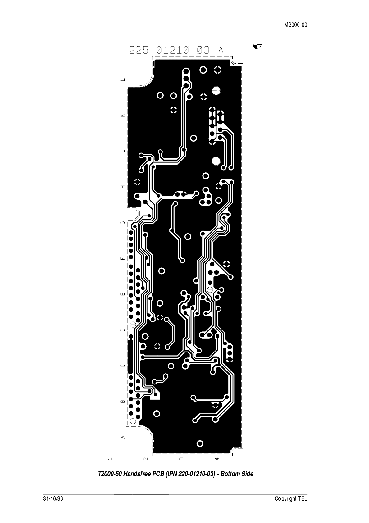
; ()(=0:;;2
123)
123)