Telit Communications S p A CC864-DUAL DUAL BAND CDMA/GPS Module User Manual User MAnual
Telit Communications S.p.A. DUAL BAND CDMA/GPS Module User MAnual
Contents
- 1. User MAnual
- 2. Users Manual
- 3. User Manual
- 4. user manual
User MAnual

CC864-Dual Hardware user manual
80pppSTzzzzza Rev. 0 - 12-Nov-07

Telit CC864-Dual Hardware user manual
80pppSTzzzzza Rev. 0 , 12-Nov-07
Reproduction forbidden without Telit wireless Solutions – All Right reserved Page 2 of 39
Contents
1. Overview ................................................................................................................................................... 4
1.1. General Specifications........................................................................................................................ 4
1.2. Receiver Specifications ...................................................................................................................... 4
1.3. Transmitter Specifications .................................................................................................................. 5
1.4. gpsOne Receiver Specifications ........................................................................................................ 5
2. Mechanical Dimensions .......................................................................................................................... 5
3. Hardware Commands .............................................................................................................................. 6
3.1. Turning ON the CC864-Dual .............................................................................................................. 6
3.2. Turning OFF the CC864-Dual ............................................................................................................ 6
3.3. Hardware shutdown ........................................................................................................................... 6
3.4. Hardware RESET Reboot .................................................................................................................. 7
4. Power Supply ........................................................................................................................................... 7
4.1. Power Supply Requirements .............................................................................................................. 7
4.2. Electrical Design Rules ...................................................................................................................... 8
4.2.1. +5V Input Source Power Supply Design Guidelines .......................................................................... 8
4.2.2. +12V Input Source Power Supply Design Guidelines ........................................................................ 8
4.2.3. Battery Source Power Supply Design Guidelines .............................................................................. 9
4.3. Battery Charge control Circuitry Design Guideline .......................................................................... 10
4.3.1. Trickle charging ................................................................................................................................. 11
4.3.2. Constant current charging ................................................................................................................ 12
4.3.3. Constant voltage charging ................................................................................................................ 12
4.3.4. Pulse charging .................................................................................................................................. 12
4.4. Thermal Design Guidelines .............................................................................................................. 13
4.5. Power Supply PCB layout Guidelines .............................................................................................. 14
5. Antenna ................................................................................................................................................... 15
5.1. Antenna Requirements ..................................................................................................................... 15
5.2. Antenna Connector .......................................................................................................................... 15
5.3. Antenna installation Guidelines ........................................................................................................ 15
6. PINs allocation ....................................................................................................................................... 16
7. Interface Description ............................................................................................................................. 20
7.1. UART1(RS232 level translation) ...................................................................................................... 20
7.1.1. 5V UART level translation ................................................................................................................ 23
7.2. R-UIM Holder ................................................................................................................................... 23
7.2.1. R-UIM Design Guidelines ................................................................................................................. 24

Telit CC864-Dual Hardware user manual
80pppSTzzzzza Rev. 0 , 12-Nov-07
Reproduction forbidden without Telit wireless Solutions – All Right reserved Page 3 of 39
7.3. USB Port .......................................................................................................................................... 24
7.4. IIC Bus Interface ............................................................................................................................... 25
7.5. ADC/DAC signals ............................................................................................................................. 25
7.6. General Purpose I/O ........................................................................................................................ 26
7.6.1. Logic level specifications .................................................................................................................. 27
7.6.2. Using a GPIO pad as Input .............................................................................................................. 27
7.6.3. Using a GPIO pad as Output............................................................................................................ 28
7.6.4. TGPIO_03/AUDIOMUTE.................................................................................................................. 28
7.6.5. TGPIO_04/CONVERSATION ........................................................................................................... 28
7.6.6. TGPIO_05/RFTXMON ..................................................................................................................... 28
7.6.7. TGPIO_06/ALARM ........................................................................................................................... 29
7.6.8. TGPIO_07/BUZZER ......................................................................................................................... 29
7.6.9. TGPIO_08/POWER_SAVING .......................................................................................................... 29
7.6.10. TGPIO_11/VIBRATOR .............................................................................................................. 30
7.6.11. TGPIO_12/CALL_KEY ............................................................................................................. 30
7.6.12. TGPIO_13/ACTIVE .................................................................................................................. 30
8. Audio Section ......................................................................................................................................... 31
8.1. Differential Audio Interface design ................................................................................................... 31
8.1.1. General Design Rules ...................................................................................................................... 31
8.1.2. Microphone design ........................................................................................................................... 32
8.2. Receiver design ................................................................................................................................ 32
8.3. Speaker design ................................................................................................................................. 33
8.4. Single-ended Audio Interface design (Hand-free or earphone design) ............................................ 33
8.5. Car kit speakerphone design ........................................................................................................... 34
8.6. PCM Interface .................................................................................................................................. 34
9. Miscellaneous signals ........................................................................................................................... 35
9.1. VAUX1 .............................................................................................................................................. 35
9.2. VRTC ................................................................................................................................................ 36
9.3. STAT_LED ........................................................................................................................................ 36
9.4. PWRMON ......................................................................................................................................... 37
9.5. AUDIO_AUX ..................................................................................................................................... 37
10. Safety Recommendations ............................................................................................................. 38
11. Reference ........................................................................................................................................ 39
12. Document Change Log .................................................................................................................. 39

Notice
OEM integrators and installers are instructed that the phrase. This device contains
transmitter FCC ID: RI7CC864-DUAL must be placed on the outside of the host.
Warning: Exposure to Radio Frequency Radiation The radiated output
power of this device is far below the FCC radio frequency exposure
limits. Nevertheless, the device should be used in such a manner that
the potential for human contact during normal operation is minimized.
In order to avoid the possibility of exceeding the FCC radio
frequency exposure limits, human proximity to the antenna should
not be less than 20cm during normal operation. The gain of the
antenna for Cellular band must not exceed-2.000 dBi.
The gain of the antenna for PCS band must not exceed -3.00000dBi.

Telit CC864-Dual Hardware user manual
80pppSTzzzzza Rev. 0 , 12-Nov-07
Reproduction forbidden without Telit wireless Solutions – All Right reserved Page 4 of 39
1. Overview
The aim of this document is the description of some hardware solutions useful for developing a
product with the Telit CC864-Dual module.
In this document all the basic functions of a mobile phone will be taken into account; for each one
of them a proper hardware solution will be suggested and eventually the wrong solutions and
common errors are to be avoided. Obviously this document can not embrace the whole hardware
solutions and products that may be designed. The wrong solutions to be avoided shall be
considered as mandatory, while the suggested hardware configuration shall not be considered
mandatory, instead the information given shall be used as a guide and a starting point for properly
developing your product with Telit CC864-Dual module. For further hardware details that may not
be explained in this document.
1.1. General Specifications
Parameters Descriptions
External Access Code Division Multiple Access
CDMA Protocol IS-95A/B, IS-98A, IS-126, IS-637A, IS-707, IS-2000
Data Rate 153.6Kbps(Full-duplex)
GPS SGPS/Standalone
Vocoder EVRC, 13kQCELP
Number of Channel 832 for Cellular, 1200 for PCS
Operating Temperature -30℃ ~ +80℃
1.2. Receiver Specifications
Parameters Descriptions
Frequency Range 869~894Mhz, 1930~1990Mhz
Sensitivity Below -104dBm
Input Dynamic Range -25dBm ~ -104dBm
Telit CC864-Dual Hardware user manual
80pppSTzzzzza Rev. 0 , 12-Nov-07
Reproduction forbidden without Telit wireless Solutions – All Right reserved Page 5 of 39
1.3. Transmitter Specifications
Parameters Descriptions
Frequency Range 824~849Mhz, 1850~1910Mhz
Power Class Class Ⅲ for Cellular, Class Ⅱ for PCS
Power Range 0.2W ~ 1.0W
Nominal Power 0.27W(24.31dBm)
1.4. gpsOne Receiver Specifications
Parameters Descriptions
Frequency Range L1, 1575.42Mhz
C/A Code 1.023Mhz Chip Rate
Receiver Sensitivity -152dBm
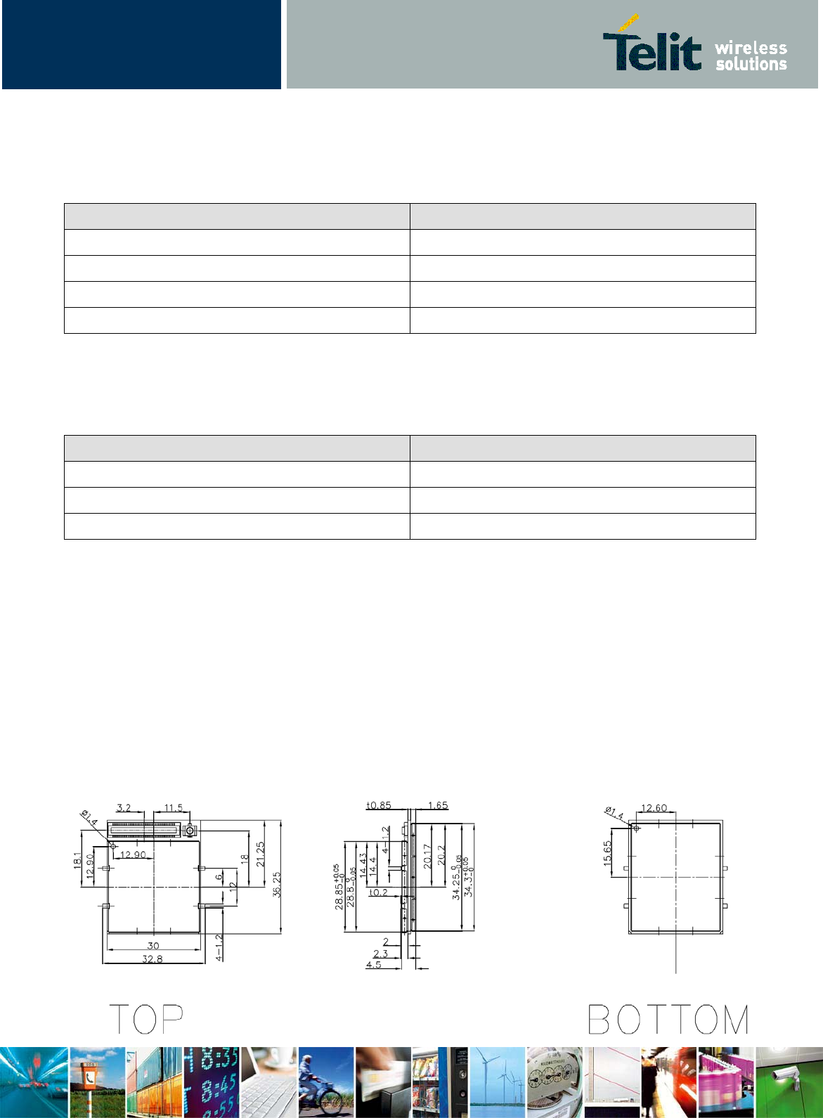
2. Mechanical Dimensions
The Telit CC864-Dual module overall dimensions are:
y Length : 36.25㎜
y Width : 30㎜
y Thickness : 4.8㎜

Telit CC864-Dual Hardware user manual
80pppSTzzzzza Rev. 0 , 12-Nov-07
Reproduction forbidden without Telit wireless Solutions – All Right reserved Page 6 of 39
3. Hardware Commands
3.1. Turning ON the CC864-Dual
To turn ON the CC864-DUAL the pad ON/OFF must be tied for at least 1 second and then released.
3.2. Turning OFF the CC864-Dual
The turning off of the device can be done in two ways:
. by software command
. by hardware shutdown
When the device is shut down by software command or by hardware shutdown, it issues to the
network a detach request that informs the network that the device will not be reachable any more.
3.3. Hardware shutdown
To turn OFF the CC864-Dual the pad ON/OFF must be tied for at least 1 second and released. The
same circuitry and timing for the power on shall be used. The device shuts down after the release
of the ON/OFF pad.

Telit CC864-Dual Hardware user manual
80pppSTzzzzza Rev. 0 , 12-Nov-07
Reproduction forbidden without Telit wireless Solutions – All Right reserved Page 7 of 39
3.4. Hardware RESET Reboot
To unconditionally Reboot the CC864-Dual, the pad RESET must be tied low for at least 200
milliseconds and the released.
A simple circuit to do it is :
4. Power Supply
The power supply circuitry and board layout are a very important part in the full product design and
they strongly reflect on the product overall performance, hence read carefully the requirements and
the guidelines for a proper design.
4.1. Power Supply Requirements
y Nominal Supply Voltage : 3.8V
y Max Supply Voltage : 4.2V
y Supply voltage range : 3.6V ~ 4.2V
y Max Peak current consumption(impulsive) : 1A
y Max Average current consumption during CDMA transmission : 700mA
y Average current during Power saving(Sleep mode) : ≤ 2mA

Telit CC864-Dual Hardware user manual
80pppSTzzzzza Rev. 0 , 12-Nov-07
Reproduction forbidden without Telit wireless Solutions – All Right reserved Page 8 of 39
The current peaks can be as high as about 1A. Therefore the power supply has to be designed in
order to withstand with these current peaks without big voltage drops; this means that both the
electrical design and the board layout must be designed for this current flow.
If the voltage goes under 3.3V, the module will be shut down automatically.
4.2. Electrical Design Rules
The electrical design of the power supply depends strongly from the power source where this
power is drained. We will distinguish them into three categories :
y +5V input(typically PC internal regulator output)
y +12V input(typically automotive)
y Battery
4.2.1. +5V Input Source Power Supply Design Guidelines
The desired output for the power supply is 3.8V, hence there’s not a big difference between the
input source and the desired output and a linear regulator can be used. A switching power supply
will not be suited because of the low drop out requirements.
When using a linear regulator, a proper heat sink shall be provided in order to dissipate the power
generated.
A Bypass low ESR capacitor of adequate capacity must be provided in order to cut the current
absorption peaks close to the CC864-Dual, a 100µF tantalum capacitor is usually suited.
Make sure the low ESR capacitor on the power supply output(usually a tantalum one) is rated at
least 10V.
A protection diode should be inserted close to the power input, in order to save the CC864-DUAL
from power polarity inversion.
4.2.2. +12V Input Source Power Supply Design Guidelines
The desired output for the power supply is 3.8V, hence due to the big difference between the input
source and the desired output, a linear regulator is not suited and shall not be used. A switching

Telit CC864-Dual Hardware user manual
80pppSTzzzzza Rev. 0 , 12-Nov-07
Reproduction forbidden without Telit wireless Solutions – All Right reserved Page 9 of 39
power supply will be preferable because of its better efficiency with the 1A peak current load
represented by the CC864-Dual.
When using a switching to the regulator, a 500㎑ or more switching frequency regulator is
preferable because of its smaller inductor size and its faster transient response. This allows the
regulator to respond quickly to the current peaks absorption.
For car PB battery the input voltage can rise up to 15.8V and this should be kept in mind when
choosing components: all components in the power supply must withstand this voltage.
A Bypass low ESR capacitor of adequate capacity must be provided in order to cut the current
absorption peaks, a 100µF tantalum capacitor is usually suited.
Make sure the low ESR capacitor on the power supply output(usually a tantalum one) is rated at
least 10V.
For car applications a spike protection diode should be inserted close to the power input, in order
to clean the supply from spikes.
A protection diode should be inserted close to the power input, in order to save the CC864-Dual
from power polarity inversion. This can be the same diode as for spike protection.
4.2.3. Battery Source Power Supply Design Guidelines
The desired nominal output for the power supply is 3.8V and the maximum voltage allowed is 4.2V,
hence a single 3.7V lithium-ion cell battery type is suited for supplying the power to the CC864-
Dual module.
The three cells Ni/Cd or Ni/MH 3.6V Nom. Battery types or 4V PB types must not be used directly
because their maximum voltage can rise over the absolute maximum voltage for the CC864-Dual
and damage it.
A Bypass low ESR capacitor of adequate capacity must be provided in order to cut the current
absorption peaks, a 100uF tantalum capacitor is usually suited.
A protection diode should be inserted close to the power input, in order to save the CC864-Dual
from power polarity inversion. Otherwise the battery connector should be done in a way to avoid
polarity inversion when connecting the battery.

Telit CC864-Dual Hardware user manual
80pppSTzzzzza Rev. 0 , 12-Nov-07
Reproduction forbidden without Telit wireless Solutions – All Right reserved Page 10 of 39
4.3. Battery Charge control Circuitry Design
Guideline
The CC864-Dual provides support circuitry for charging a lithium-ion battery, utilizing as many as
four software-enabled charging techniques: trickle, constant current, constant voltage, and pulsed.
Battery voltage, external supply voltage, and total detected current measurements are available to
software through the analog multiplexer. This allows the software device to monitor charging
parameters, make decisions, and control the charging process.
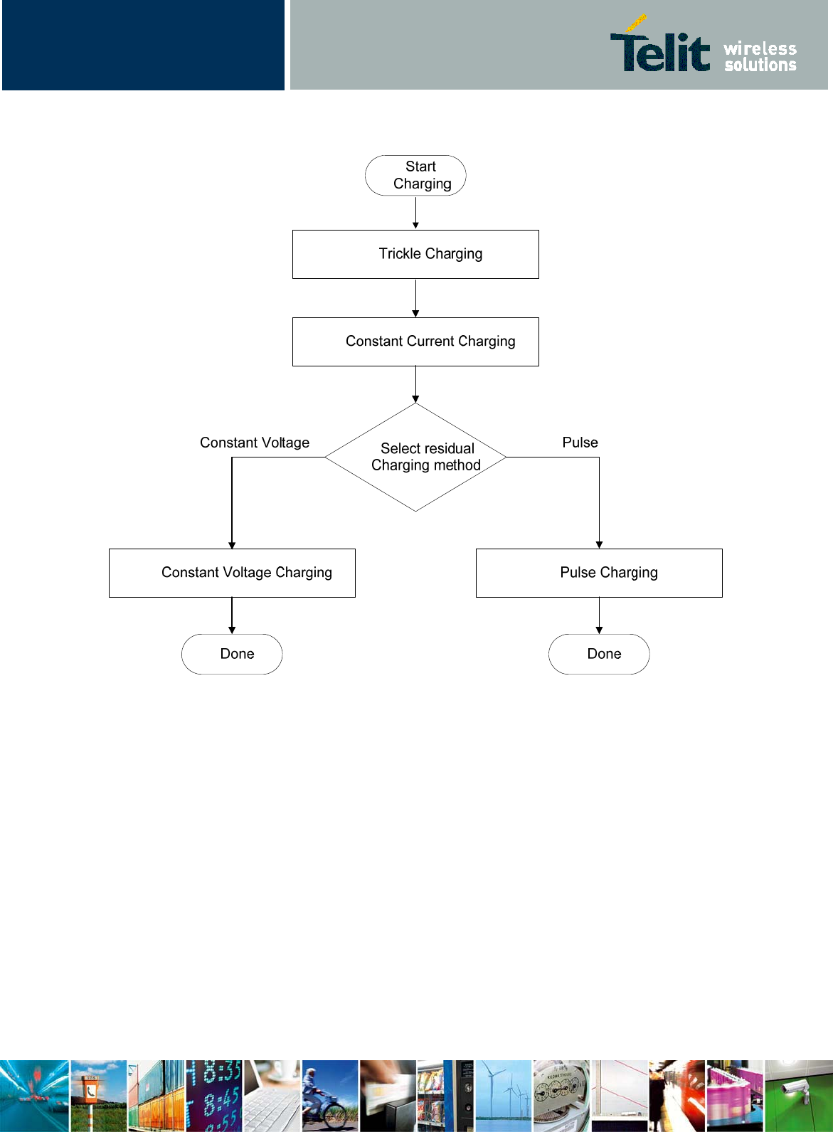
Charging begins with trickle charging, a mode that limits the current and avoids pulling VDD down.
Once a minimum battery voltage is established using trickle charging, constant current charging is
enabled via software to charge the battery quickly - this mode is sometimes called fast charging.
Once the Li-ion battery approaches its target voltage (through constant current charging), the
charge is completed using either constant voltage or pulse charging. Further discussion of all
charging modes is provided in the sections identified within bellowed picture.
The main battery charging sequence is
Telit CC864-Dual Hardware user manual
80pppSTzzzzza Rev. 0 , 12-Nov-07
Reproduction forbidden without Telit wireless Solutions – All Right reserved Page 11 of 39
4.3.1. Trickle charging
Trickle charging of the main battery, enabled through software control and powered from Vdd, is
provided by the CC864-Dual. This mode is used to raise a severely depleted battery’s voltage to a
level sufficient to begin fast charging.
Fast charging with a high-current supply should not be attempted on a deeply discharged battery –
the battery would draw excessive current, pull the Vdd voltage down, and possibly cause a
handset malfunction or shutdown due to an under-voltage lockout condition. If the CC864-Dual
implements current limiting, the excessive current would combine with the potentially large voltage
drop across the pass transistor to generate unwanted heat within the device. To avoid these
problems the CC864-Dual provides a constant, low-current charging mode - trickle charging.
Trickle charging is enabled through software control and should be used until the main battery

Telit CC864-Dual Hardware user manual
80pppSTzzzzza Rev. 0 , 12-Nov-07
Reproduction forbidden without Telit wireless Solutions – All Right reserved Page 12 of 39
reaches its desired threshold, usually about 3.0V for Li-ion batteries. The threshold varies with
battery type and application, so there is no predefined value implemented in the detection circuits.
Software must terminate trickle charging based on battery voltage measurements and the battery
type – there is not a preset termination threshold.
4.3.2. Constant current charging
The CC864-Dual supports constant current charging of the main battery. During constant current
charging the battery is charged with a constant current(600mA). As the battery voltage rises and
approaches its desired value(4.2V) the charging current begins to decrease. This is the end of
constant current charging and the beginning of residual charging. The target value is set by SBI-
programming to a value higher than the desired final voltage to overcome the battery internal ESR
and achieve faster charging. Software monitors the voltage and takes the appropriate action to
terminate the constant current charging mode. Charging continues with residual charging(either
constant voltage or pulsed).
4.3.3. Constant voltage charging
Once constant current charging of a lithium-ion battery is finished, the charging continues using
either constant voltage or pulsed techniques.
The constant voltage charging is very similar to its constant current mode. The battery voltage is
constant(or nearly so) while the charging current decreases exponentially for the remaining
charger process.
The end of constant voltage charging is typically detected by allowing voltage operation for a
predetermined duration beyond crossing the VBATDET threshold in the charger IC(on the order of
one-half to two hours). It is important to limit this predetermined duration – do not allow charging to
continue indefinitely! Charging too long will damage the battery….consult battery manufacturers for
specific recommendations.
4.3.4. Pulse charging
Pulse charging is implemented by switching the pass transistor in the charger IC on and off ; phone

Telit CC864-Dual Hardware user manual
80pppSTzzzzza Rev. 0 , 12-Nov-07
Reproduction forbidden without Telit wireless Solutions – All Right reserved Page 13 of 39
electronics should draw minimal current so the battery’s open circuit voltage can be measured
accurately during the off interval.
Pulse charging, compared to constant voltage charging, provides better voltage accuracy, reaches
full charge more quickly, and dissipates less transistor power when switching from constant current
charging. Pulse charging is enabled through software control, uses the same hardware as constant
current or constant voltage charging, but repetitiously opens and closes the pass transistor to
deliver current pulses to the battery.
As the battery charges it reaches the VBADET threshold, causing the internal charger IC counter
T_ON to start. The pass transistor stays closed(and the battery continues charging) until the T_ON
counter expires. Then the pass transistor is opened, charging stops, and another internal
counter(T_OFF) is enabled. Without continued charging, the battery voltage may drop-if it drops
too far, additional charging is needed. If it holds its voltage, it is fully charged and the charging
process is terminated. This is one purpose of pulsed operation – to check and recheck the
battery’s open circuit voltage, confirming a full charger before terminating the process.
4.4. Thermal Design Guidelines
The thermal design for the power supply heat sink should be done with the following specification:
y Average current consumption during transmission at Max level : 700mA
y Average current consumption during transmission at Min level : 220mA
y Average current during Idle mode : 60mA
y Average current during sleep mode : 1mA
y Average current during hibernation mode : 275nA
Considering the very low current during idle, especially if Power Saving function is enabled, it is
possible to consider from the thermal point of view that the device absorbs current significantly only
during calls.
If we assume that the device stays into transmission for short periods of time(let’s say few minutes)
and then remains for a quite long time in idle(let’s say one hour), then the power supply has always
the time to cool down between the calls and the heat sink could be smaller than the calculated one
for 700mA maximum RMS current, or even could be the simple chip package(no heat sink)
Moreover in the average network conditions the device is requested to transmit at a lower power

Telit CC864-Dual Hardware user manual
80pppSTzzzzza Rev. 0 , 12-Nov-07
Reproduction forbidden without Telit wireless Solutions – All Right reserved Page 14 of 39
level than the maximum and hence the current consumption will be less than 700mA.
For these reasons the thermal design is rarely a concern and the simple ground plane where the
power supply chip is placed can be enough to ensure a good thermal condition and avoid
overheating. This generated heat will be mostly conducted to the ground plane under the CC864-
DUAL, you must ensure that your application can dissipate it.
4.5. Power Supply PCB layout Guidelines
The Bypass low ESR capacitor must be placed close to the CC864-Dual power input pads or in the
case the power supply is a switching type it can be placed close to the inductor to cut the ripple
provided the PCB trace from the capacitor to the CC864-Dual is wide enough to ensure a dropless
connection even during the 1A current peaks.
The protection diode must be placed close to the input connector where the power source is
drained.
The PCB traces from the input connector to the power regulator IC must be wide enough to ensure
no voltage drop occur when the 1A current peaks are absorbed.
The PCB traces to the CC864-Dual and Bypass capacitor must be wide enough to ensure no
significant voltage drops occur when the 1A current peaks are absorbed. Try to keep this traces as
short as possible.
The PCB traces connecting the Switching output to the inductor and the switching diode must be
kept as short as possible by placing the inductor and the diode very close to the power switching
IC(only for switching power supply). This is done in order to reduce the radiated field(noise) at the
switching frequency(100~500㎑ usually)
The use of a good common ground plane is suggested.
The placement of the power supply on the board should be done in such a way to guarantee that
the high current return paths in the ground plane are not overlapped to any noise sensitive circuitry
as the microphone amplifier/buffer or earphone amplifier.
The power supply input cables should be kept separate from noise sensitive lines such as
microphone/earphone cables.

Telit CC864-Dual Hardware user manual
80pppSTzzzzza Rev. 0 , 12-Nov-07
Reproduction forbidden without Telit wireless Solutions – All Right reserved Page 15 of 39
5. Antenna
The antenna connection and board layout are the most important part in the full product design and
they strongly reflect on the product overall performance, hence read carefully the requirements and
the guidelines for a proper design.
5.1. Antenna Requirements
Parameters Descriptions
Frequency range(CDMA) Tx : 824㎒ ~ 849, Rx : 869 ~ 894㎒
Frequency range(PCS) Tx : 1850㎒ ~ 1910㎒, Rx : 1930㎒ ~ 1990㎒
Frequency range(GPS) 1575.42㎒
Impedance 50Ω
VSWR recommended ≤ 2
Radiation pattern Omni-directional
Polarization Vertical
Furthermore if the device is developed for the US market and/or Canada market, it shall comply to
the FCC and/or IC approval requirements:
5.2. Antenna Connector
The CC864-Dual module is equipped with a 50 Ohm RF connector from Murata, GSC type and
P/N MM9329-2700RA1. The counterpart suitable is Murata MXTK92 type or MXTK88 type.
5.3. Antenna installation Guidelines
Install the antenna in a place covered by the CDMA signal
Antenna shall not be installed inside metal cases
Antenna shall be installed also according Antenna manufacturer instructions

Telit CC864-Dual Hardware user manual
80pppSTzzzzza Rev. 0 , 12-Nov-07
Reproduction forbidden without Telit wireless Solutions – All Right reserved Page 16 of 39
6. PINs allocation
The CC864-DUAL uses an 80 pin Molex p.n 53949-0878 male connector for the connections with
the external applications. This connector matches the 54150-0878 model.
Pin Signal I/O Function Internal
Pull up Type
Power Supply
1 VBATT - Main power supply Power
2 VBATT - Main power supply Power
3 VBATT - Main power supply Power
4 VBATT - Main power supply Power
5 GND - Ground Power
6 GND - Ground Power
7 GND - Ground Power
Audio
8 AXE I Handsfree switching 100kΩ CMOS 2.8V
9 EAR_HF+ AO Handsfree ear output, phase+ Audio
10 EAR_HF- AO Handsfree ear output, phase- Audio
11 EAR_MT+ AO Handset earphone signal output, phase+ Audio
12 EAR_MT- AO Handset earphone signal output, phase- Audio
13 MIC_HF+ AI Handsfree microphone input ; phase+, nominal
level
3mVrms
Audio
14 MIC_HF- AI Handsfree microphone input ; phase-, nominal
level
3mVrms
Audio
15 MIC_MT+ AI Handset microphone signal input ; phase+,
nominal level
50mVrms
Audio
16 MIC_MT- AI Handset microphone signal input ; phase-,
nominal level 50mVrms
Audio
R-UIM Card Interface
18 UIM_PWR - Power supply for the UIM 2.8V

Telit CC864-Dual Hardware user manual
80pppSTzzzzza Rev. 0 , 12-Nov-07
Reproduction forbidden without Telit wireless Solutions – All Right reserved Page 17 of 39
19 UIM_RST O Reset 2.8V
20 UIM_DATA I/O Data I/O 2.8V
21 UIM_IN I Presence(active low) 47kΩ 2.8V
22 UIM_CLK O Clock 2.8V
QCOM Diagnostic Monitor
23 RX_TRACE I RX Data for debug monitor CMOS 2.8V
24 TX_TRACE O TX Data for debug monitor CMOS 2.8V
Prog. / Data + Hw Flow Control
25 C103/TXD I Serial data input (TXD) from DTE CMOS 2.8V
26 C104/RXD O Serial data output to DTE CMOS 2.8V
27 C107/DSR O Output for Data set ready signal (DSR) to DTE CMOS 2.8V
28 C106/CTS O Output for Clear to send signal (CTS) to DTE CMOS 2.8V
29 C108/DTR I Input for Data terminal ready signal (DTR) from
DTE
CMOS 2.8V
30 C125/RING O Output for Ring indicator signal (RI) to DTE CMOS 2.8V
31 C105/RTS I Input for Request to send signal (RTS) from DTE CMOS 2.8V
32 C109/DCD O Output for Data carrier detect signal (DCD) to
DTE
CMOS 2.8V
IIC
33 SCL I/O IIC Hardware interface CMOS 2.8V
34 SDA I/O IIC Hardware interface CMOS 2.8V
USB
35 USB_ID I USB_ID input 47kΩ CMOS 2.8V
48 USB_VBUS AI/A
O
USB_VBUS power supply 5V
79 USB_D+ I/O USB Data(USB Internal Transceiver In/Output) 2.8V~3.6V
80 USB_D- I/O USB Data(USB Internal Transceiver In/Output) 2.8V~3.6V
DAC and ADC
37 ADC_IN1 AI Analog/Digital converter input A/D
38 ADC_IN2 AI Analog/Digital converter input A/D
39 ADC_IN3 AI Analog/Digital converter input A/D
40 DAC_OUT AO Digital/Analog converter output D/A(PWM)
PCM
36 PCM_CLOCK I/O Telit GPIO Configurable GPIO CMOS 2.8V

Telit CC864-Dual Hardware user manual
80pppSTzzzzza Rev. 0 , 12-Nov-07
Reproduction forbidden without Telit wireless Solutions – All Right reserved Page 18 of 39
63 TGPIO_10/PCM_T
X
I/O Telit GPIO10 Configurable GPIO CMOS 2.8V
65 TGPIO_18/PCM_
RX
I/O Telit GPIO18 Configurable GPIO CMOS 2.8V
71 TGPIO_17/PCM_
SYNC
I/O Telit GPIO17 Configurable GPIO CMOS 2.8V
Miscellaneous Functions
45 STAT_LED O Status indicator led CMOS 1.8V
46 GND - Ground Ground
49 PWRMON O Power ON Monitor CMOS 2.8V
50 VAUX1 - Power output for external accessories (AT
command driven)
2.85V/
150mA
51 CHARGE AI Charger input Li-Ion Power
52 CHARGE AI Charger input Li-Ion Power
53 ON/OFF* I Input command for switching power ON or OFF
(toggle command). The pulse to be sent to the
CC864-DUAL must be equal or greater than 1
second.
47kΩ Pull up to
VBTT
54 RESET* I Reset input
55 VRTC Power
Telit GPIO
56 TGPIO_19 I/O Telit GPIO19 Configurable GPIO CMOS 2.8V
57 TGPIO_11/VIBRA
TOR
I/O Telit GPIO11 Configurable GPIO/Vibrator CMOS 2.8V
58 TGPIO_20 I/O Telit GPIO20 Configurable GPIO CMOS 2.8V
59 TGPIO_04/CONV
ERSATION
I/O Telit GPIO4 Configurable GPIO/Conversation CMOS 2.8V
60 TGPIO_14 I/O Telit GPIO14 Configurable GPIO CMOS 2.8V
61 TGPIO_15 I/O Telit GPIO15 Configurable GPIO CMOS 2.8V
62 TGPIO_12/AUDIO
CALL BUTTON
I/O Telit GPIO12 Configurable GPIO/Audio Call
Button
CMOS 2.8V
64 TGPIO_22 I/O Telit GPIO22 Configurable GPIO CMOS 1.8V
66 TGPIO_03/AUDIO
MUTE
I/O Telit GPIO03 Configurable GPIO/Audio Mute CMOS 2.8V

Telit CC864-Dual Hardware user manual
80pppSTzzzzza Rev. 0 , 12-Nov-07
Reproduction forbidden without Telit wireless Solutions – All Right reserved Page 19 of 39
67 TGPIO_08/POWE
R_SAVING
I/O Telit GPIO08 Configurable GPIO/Power saving
mode
CMOS 2.8V
68 TGPIO_06/ALAR
M
I/O Telit GPIO06 Configurable GPIO/Power wakeup CMOS 2.8V
70 TGPIO_01 I/O Telit GPIO01 Configurable GPIO CMOS 2.8V
72 TGPIO_21 I/O Telit GPIO21 Configurable GPIO CMOS 2.8V
73 TGPIO_07/BUZZE
R
I/O Telit GPIO07 Configurable GPIO/Buzzer CMOS
2.8V(PWM)
74 TGPIO_02 I/O Telit GPIO02 Configurable GPIO CMOS 2.8V
75 TGPIO_16 I/O Telit GPIO16 Configurable GPIO CMOS 2.8V
76 TGPIO_09 I/O Telit GPIO09 Configurable GPIO CMOS 2.8V
77 TGPIO_13/ACTIV
E
I/O Telit GPIO13 Configurable GPIO/ACTIVE pin to
protect current leakage
CMOS 2.8V
78 TGPIO_05/RFTX
MON
I/O Telit GPIO05 Configurable GPIO/Transmitter ON
monitor
CMOS 2.8V
Reserved
17
41
42
43
44
47
48
69
79
80

Telit CC864-Dual Hardware user manual
80pppSTzzzzza Rev. 0 , 12-Nov-07
Reproduction forbidden without Telit wireless Solutions – All Right reserved Page 20 of 39
7. Interface Description
This chapter covers information required to convert the CC864-Dual into a subscriber unit
application.
And this chapter include :
y UART1 : RS232 level translation for AT command
y R-UIM card holder
y USB
y IIC BUS Interface
y ADC/DAC signals
y General Purpose I/O
7.1. UART1(RS232 level translation)
The serial port on the CC864-DUAL is the core of the interface between the module and Host
hardware.
Depending from the type of serial port on the Host hardware, a level translator circuit may be
needed to make the system work. The only configuration that doesn’t need a level translation is the
2.8V UART.
There are two UART port on the CC864-Dual. It differs from the PC RS232 in the signal
polarity(RS232 is reversed) and levels. The levels for the CC864-Dual UART are the CMOS levels:
Absolute maximum ratings – Not functional
Parameter Min Max
Input level on any digital pin when on -0.3V +3.75V
Input voltage on analog pins when on -0.3V +3.0V
Operating Range – Interface levels(2.8V CMOS)
Level Min Max
Input high level VIH 1.85V 3.15V

Telit CC864-Dual Hardware user manual
80pppSTzzzzza Rev. 0 , 12-Nov-07
Reproduction forbidden without Telit wireless Solutions – All Right reserved Page 21 of 39
Input low level VIL -0.3V 0.9V
Output high level VOH 2.4V 2.85V
Output low level VOL 0.0V 0.45V
UART1 is used for interfacing between the CC864-Dual and Host. The CC864-Dual and its host
transmit data or AT-command through RS-232 signal line.
The signals of the CC864-Dual serial port are:
RS232
Pin Nr Signal PIN
Number Name Usage
1 DCD-
dcd_uart
32 Data Carrier Detect Output from the CC864-Dual that
indicates the carrier presence
2 RXD-tx_uart 26 Transmit line Output transmit line of CC864-Dual
UART
3 TXD-rx_uart 25 Receive line Input receive of the CC864-Dual
UART
4 DTR-dtr_uart 29 Data Terminal
Ready
Input to the CC864-Dual that control
the DTE READY condition
5 GND 5,6,7 Ground Ground
6 DSR-dsr_uart 27 Data Set Ready Output from the CC864-Dual that
indicates the module is ready
7 RTS-rts_uart 31 Request to Send Input to the CC864-Dual that
controls the Hardware flow control
8 CTS-cts_uart 28 Clear to Send Output from the CC864-Dual that
controls the Hardware flow control
9 RI-ri_uart 30 Ring Indicator Output from the CC864-Dual that
indicates the incoming call condition
In order to interface the CC864-Dual with a PC com port or a RS232(EIA/TIA-232) application a
level translator is required. This level translator must
invert the electrical signal in both directions
change the level from 0/3V to 15/-15V
Actually, the RS232 UART 16450, 16550, 16650 & 16750 chipsets accepts signals with lower
levels on the RS232 side(EIA/TIA-562), allowing for a lower voltage-multiplying ratio on the level
translator. Note that the negative signal voltage must be less than 0V and hence some sort of level
translation is always required.
Telit CC864-Dual Hardware user manual
80pppSTzzzzza Rev. 0 , 12-Nov-07
Reproduction forbidden without Telit wireless Solutions – All Right reserved Page 22 of 39
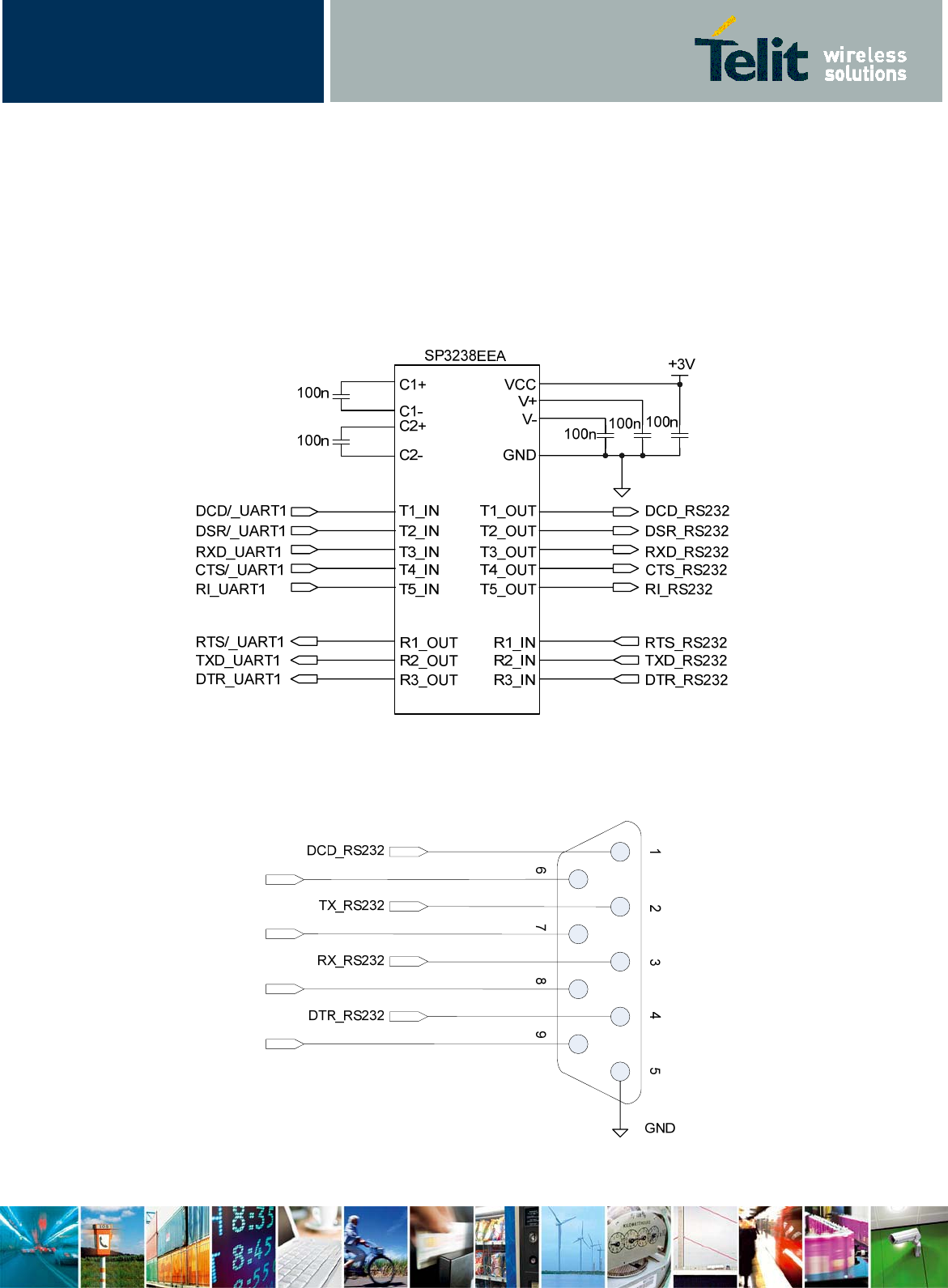
By convention the driver is the level translator from the 0-3V UART level to the RS232 level, while
the receiver is the translator from RS232 level to 0-3V UART.
In order to translate the whole set of control lines of the UART you will need: 5 driver and 3
receiver
An example of level translation circuitry of this kind is :
The RS232 serial port lines are usually connected to a DB9 connector with the following layout :
Telit CC864-Dual Hardware user manual
80pppSTzzzzza Rev. 0 , 12-Nov-07
Reproduction forbidden without Telit wireless Solutions – All Right reserved Page 23 of 39
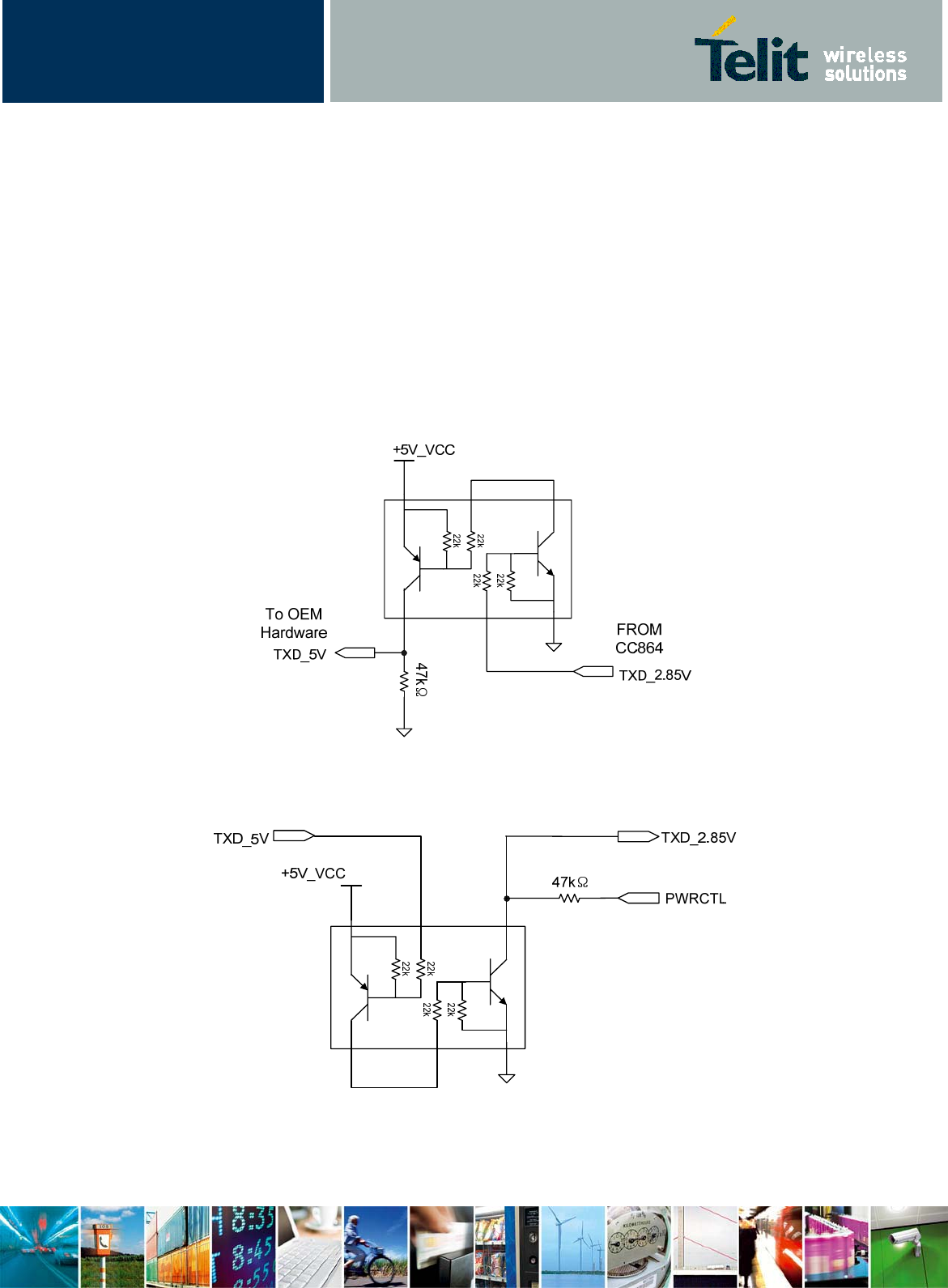
7.1.1. 5V UART level translation
If the Host application uses a microcontroller with a serial port(UART) that works at a voltage
different from 2.8~3V, then a circuitry has to be provided to adapt the different levels of the two sets
of signals. As for the RS232 translation there are a multiple of single chip translators, but since the
translation requires very few components, then also a discrete design can be suited. For example
a possible inexpensive translator circuit for a 5V driver can be:
And for a 5V receiver:
7.2. R-UIM Holder

Telit CC864-Dual Hardware user manual
80pppSTzzzzza Rev. 0 , 12-Nov-07
Reproduction forbidden without Telit wireless Solutions – All Right reserved Page 24 of 39
The Removable User Identify Module(R-UIM) is a smart card for CDMA cellular applications. R-
UIM provides personal authentication information which allows the mobile station or handset to be
connected with the network. The R-UIM card enables handset independence for the user. The R-
UIM card can be inserted into any CDMA R-UIM equipped handset, allowing the user to receiver or
make calls and receive other subscribed services from any R-UIM equipped handset.
7.2.1. R-UIM Design Guidelines
Aim of this section is to give basic design guide lines to integrate a R-UIM holder in applications
that uses
Pin NO. Signal Name Signal Description Direction
18 VREG_UIM_PWR_2.85V Power supply CC864-Dual → R-UIM
19 UIM_RST Reset signal CC864-Dual → R-UIM
20 UIM_DATA Serial data CC864-Dual ↔ R-UIM
21 UIM_IN NC
22 UIM_CLK Clock CC864-Dual → R-UIM
7.3. USB Port
The CC864-Dual includes a universal serial bus(USB) transceiver. This transceiver operates at
USB low-speed(1.5Mbits/sec) and USB full-speed(12Mbits/sec). It is complaint with USB 2.0
specification. It can be used for diagnostic monitoring purpose.
Pin
Number Signal Usage
35 USB_ID Analog input used to sense whether a peripheral device is connected,
and determine the peripheral type, a host or a slave
48 USB_VBUS
Power supply for the internal USB transceiver. This pin is configured as
an analog input or and analog output depending upon the type of
peripheral device connected.
79 USB_D+ Plus(+) line of the differential, bi-directional USB signal to/from the

Telit CC864-Dual Hardware user manual
80pppSTzzzzza Rev. 0 , 12-Nov-07
Reproduction forbidden without Telit wireless Solutions – All Right reserved Page 25 of 39
peripheral device
80 USB_D- Minus(+) line of the differential, bi-directional USB signal to/from the
peripheral device
7.4. IIC Bus Interface
I2C is a two-wire bus for inter-IC communication that supports any IC fabrication process(NMOS,
CMOS, bipolar, etc). Two wires(or lines), serial data(SDA) and serial clock(SCL), carry information
between the connected devices. Each device is recognized by a unique address(whether it’s a
microcontroller, memory, LCD driver, stereo DAC, or keyboard interface) and can operate as either
a transmitter or receiver, depending on the device function.
Pin No Name Description
33 SCL Serial BUS Clock
34 SDA Serial BUS Data
7.5. ADC/DAC signals
Analog measurement output or sensor output(Battery voltage, temperature etc) can be connected
to ADC pin. Then it change analog value to digital.
DAC pin drive out PWM signal and control external component. And you need additional RC filter
to change PWM signal to analog signal.
Pin No Name Description Direction
37 ADC_IN1 Analog/Digital converter
input
→ CC864-Dual
38 ADC_IN2 Analog/Digital converter
input
→ CC864-Dual
39 ADC_IN3 Analog/Digital converter
input
→ CC864-Dual
40 DAC_OUT Digital/Analog converter
input
← CC864-Dual

Telit CC864-Dual Hardware user manual
80pppSTzzzzza Rev. 0 , 12-Nov-07
Reproduction forbidden without Telit wireless Solutions – All Right reserved Page 26 of 39
7.6. General Purpose I/O
The general purpose I/O pads can be configured to act in three different ways:
y input : Input pads can only be read and report the digital value(high or low) present on
the pad at the read time
y output : output pads can only be written or queried and set the value of the pad output
y alternate function(internally controlled) : an alternate function pad is internally
controlled by the CC864-Dual firmware and acts depending on the function
implemented.
Pin Signal I/O Function Type Default
state
On_OFF
state
Alternative
Function
70 TGPIO_01 I/O Gonfigurable GPIO CMOS2.8V Input Low
74 TGPIO_02 I/O Gonfigurable GPIO CMOS2.8V Input Low JDR
66 TGPIO_03 I/O Gonfigurable GPIO CMOS2.8V Input Low AUDIO MUTE
59 TGPIO_04 I/O Gonfigurable GPIO CMOS2.8V Input Low CONVERSATION
78 TGPIO_05 I/O Gonfigurable GPIO CMOS2.8V Input Low RFTXMON
68 TGPIO_06 I/O Gonfigurable GPIO CMOS2.8V Input ALARM
73 TGPIO_07 I/O Gonfigurable GPIO CMOS2.8V Input Low BUZZER
67 TGPIO_08 I/O Gonfigurable GPIO CMOS2.8V Input Low POWER_SAVING
76 TGPIO_09 I/O Gonfigurable GPIO CMOS2.8V Input Low
63 TGPIO_10 I/O Gonfigurable GPIO CMOS2.8V Input Low PCM_TX
57 TGPIO_11 I/O Gonfigurable GPIO CMOS2.8V Input Low VIBRATOR
62 TGPIO_12 I/O Gonfigurable GPIO CMOS2.8V Input Low CALL_KEY
77 TGPIO_13 I/O Gonfigurable GPIO CMOS2.8V Input Low ACTIVE
60 TGPIO_14 I/O Gonfigurable GPIO CMOS2.8V Input Low
61 TGPIO_15 I/O Gonfigurable GPIO CMOS2.8V Input Low
75 TGPIO_16 I/O Gonfigurable GPIO CMOS2.8V Input Low
71 TGPIO_17 I/O Gonfigurable GPIO CMOS2.8V Input Low PCM_SYNC
65 TGPIO_18 I/O Gonfigurable GPIO CMOS2.8V Input Low PCM_RX
56 TGPIO_19 I/O Gonfigurable GPIO CMOS2.8V Input Low
58 TGPIO_20 I/O Gonfigurable GPIO CMOS2.8V Input Low
Telit CC864-Dual Hardware user manual
80pppSTzzzzza Rev. 0 , 12-Nov-07
Reproduction forbidden without Telit wireless Solutions – All Right reserved Page 27 of 39
72 TGPIO_21 I/O Gonfigurable GPIO CMOS2.8V Input Low
64 TGPIO_22 I/O Gonfigurable GPIO CMOS2.8V Input Low
7.6.1. Logic level specifications
Where not specifically stated, all the interface circuits work at 2.8V CMOS logic levels. The
following tables shows the logic level specifications used in the CC864-Dual interface circuits :
Absolute maximum ratings – Not functional
Parameter Min Max
Input level on any digital pin when
on
-0.3V +3.75V
Input voltage on analog pins when
on
-0.3V +3.0V
Operating Range – Interface levels(2.8V CMOS)
Level Min Max
Input high level VIH 1.85V 3.15V
Input low level VIL -0.3V 0.9V
Output high level VOH 2.4V 2.85V
Output low level VOL 0.0V 0.45V
For 1.8V
Operating Range – Interface levels(1.8V CMOS)
Level Min Max
Input high level 1.6V 2.1V
Input low level -0.3V 0.63V
Output high level 1.35V 1.8V
Output low level 0.0V 0.35V
7.6.2. Using a GPIO pad as Input

Telit CC864-Dual Hardware user manual
80pppSTzzzzza Rev. 0 , 12-Nov-07
Reproduction forbidden without Telit wireless Solutions – All Right reserved Page 28 of 39
The GPIO pads, when used as input, can be connected to a digital output of another device and
report its status, provided this device has interface levels compatible with the 2.8V CMOS levels of
the GPIO
7.6.3. Using a GPIO pad as Output
The GPIO pads, when used as outputs, can drive 2.8V CMOS digital devices or compatible
hardware. When set as outputs, the pads have a push-pull output and therefore the pull-up resistor
may be omitted.
7.6.4. TGPIO_03/AUDIOMUTE
This pin can be used to mute audio. It is always desirable to have a mute control on the amplifier,
in order to turn it off while the device is not sending signal to the output, in this matter the amplifier
background noise which may be audible during idle condition is cut off.
7.6.5. TGPIO_04/CONVERSATION
This signal can be used as the audio amplifier enable control signal when the modem uses the
audio amplifier on its receiver speaker output layer. It will reduce current consumption because it
can activate the amplifier only when there is voice data.
7.6.6. TGPIO_05/RFTXMON
This pin will be changed to High state when CC864-DUAL is transmitting state.

Telit CC864-Dual Hardware user manual
80pppSTzzzzza Rev. 0 , 12-Nov-07
Reproduction forbidden without Telit wireless Solutions – All Right reserved Page 29 of 39
7.6.7. TGPIO_06/ALARM
This pin, when configured as Alarm Output, is controlled by the CC864-Dual module and will rise
when the alarm starts and fall after the issue of a dedicated AT command.
This output can be used to power up the CC864-Dual controlling microcontroller or application at
the alarm time, giving you the possibility to program a timely system wake-up to achieve some
periodic actions and completely turn off either the application and the CC864-Dual during sleep
periods, dramatically reducing the sleep consumption to few ㎂. In battery powered devices this
feature will greatly improve the autonomy of the device.
7.6.8. TGPIO_07/BUZZER
This pin, when configured as Buzzer Output, is controlled by the CC864-Dual module and will drive
with appropriate square waves a Buzzer driver. This permits to your application to easily implement
Buzzer feature with ringing tones or melody played at the call incoming, tone playing on SMS
incoming or simply playing a tone or melody when needed by your application.
The example is :
7.6.9. TGPIO_08/POWER_SAVING
The Host gives this signal to the CC864-Dual, it makes the CC864-Dual turn to be power saving

Telit CC864-Dual Hardware user manual
80pppSTzzzzza Rev. 0 , 12-Nov-07
Reproduction forbidden without Telit wireless Solutions – All Right reserved Page 30 of 39
mode. This signal is Low enable. When the CC864-Dual enters into power saving mode, every
active items include UART port will be off. So current consumption is considerably reduced.
And the CC864-Dual monitors the TXD line state of UART1. If the state will be changed Low state,
the CC864-Dual will turn to be power saving mode automatically.
The application developer must keep in mind that this signal and TXD line state of UART1 perform
same function. So if one of the both becomes Low state , the CC864-Dual will turn to be power
saving mode.
7.6.10. TGPIO_11/VIBRATOR
When configured as VIBRATOR output, this pin is controlled by the CC864-Dual module and will
drive with appropriate square waves. Refer the Buzzer circuitry.
7.6.11. TGPIO_12/CALL_KEY
When Earjack is inserted, this pin is used to connect outgoing call or response incoming call.
7.6.12. TGPIO_13/ACTIVE
This signal is used as an enable signal to control the buffer between CC864-Dual and the host.
When reset procedure and boot sequence are done successfully, CC864-Dual drives ACTIVE
signal to be High state. And its output is Low state when CC864-Dual is power off. So a pull-down
resistor is needed to be clear its state.
Most of the signals(except ON/OFF, RESET, STAT_LED) between CC864-Dual and host must use
a buffer. It prevents leakage currents flow from Host that is power-on stated to CC864-Dual that is
power-off stated. Leakage current could cause CC864-Dual to reset failure.

Telit CC864-Dual Hardware user manual
80pppSTzzzzza Rev. 0 , 12-Nov-07
Reproduction forbidden without Telit wireless Solutions – All Right reserved Page 31 of 39
8. Audio Section
The CC864-DUAL module provides two different audio blocks; both in transmit(Uplink) and in
receive(Downlink) direction:
“MT lines” should be used for handset function,
“HF lines” is suited for hands-free function or earphone function.
These two blocks can be active only one at a time, selected by AXE hardware line or by AT
command.
The audio characteristics are equivalent in transmit blocks, but are different in the receive ones
and this should be kept in mind when designing.
8.1. Differential Audio Interface design
You can use the MIC_MT+, MIC_MT-, EAR_MT+, EAR_MT-.
8.1.1. General Design Rules

Telit CC864-Dual Hardware user manual
80pppSTzzzzza Rev. 0 , 12-Nov-07
Reproduction forbidden without Telit wireless Solutions – All Right reserved Page 32 of 39
There are several configuration for the audio paths, but the most difference is between balanced
and unbalanced microphone configuration.
It is highly recommended to keep the whole microphone path balanced even if this means having
2wires connecting the microphone instead of one needed in the unbalanced case. The balanced
circuitry is more suited because of its good common mode noise rejection.
Keep the microphone traces on the PCB and wires as short as possible.
If your application requires an unbalanced microphone, then keep the lines on the PCB balanced
and “unbalance” the path close to the microphone wire connector if possible.
Make sure that the microphone traces in the PCB don’t cross or run parallel to noisy
traces(especially the power line).
If possible put all around to the microphone lines a ground trace connected to the ground plane by
several vias. This is done in order to simulate a shielded trace on the PCB.
The CC864-DUAL provides two audio paths in receive section. Only one of the paths can be active
at a time, selectable by AXE hardware line or by AT command.
8.1.2. Microphone design
You need an additional external bias circuitry.
The example is :
8.2. Receiver design
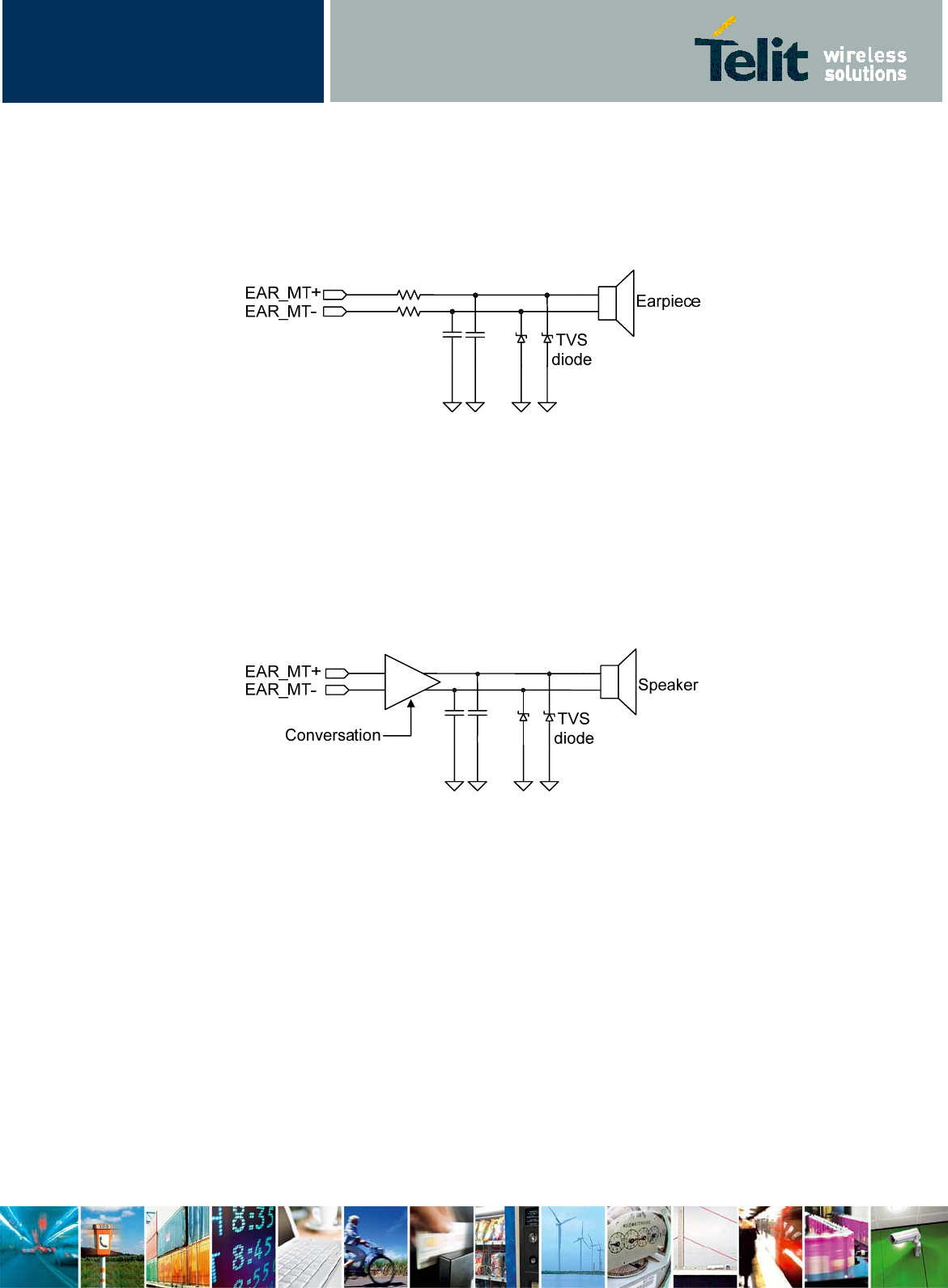
The EAR_MT+, EAR_MT- are the differential line-out drivers. You can drive directly a 16Ω earpiece
Telit CC864-Dual Hardware user manual
80pppSTzzzzza Rev. 0 , 12-Nov-07
Reproduction forbidden without Telit wireless Solutions – All Right reserved Page 33 of 39
and don’t need an external audio amplifier circuitry. This solution is often the most cost effective,
reducing the components count to a minimum.
The example is :
8.3. Speaker design
The EAR_MT+, EAR_MT- are the differential line-out drivers. You can drive a 8Ω speaker with an
external audio amplifier. This solution is can be used when high audio power is needed.
The example is :
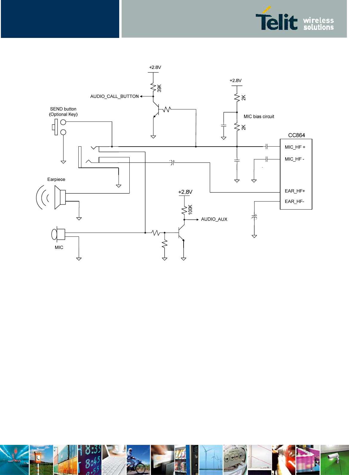
8.4. Single-ended Audio Interface design (Hand-
free or earphone design)
You can use the MIC_HF+, MIC_HF-, EAR_HF+, EAR_HF-.
Additional MIC_HF+ bias circuitry, AUDIO_AUX circuitry, AUDIO_CALL_BUTTON circuitry are
needed.
AUDIO_AUX will be used to notify if earphone is inserted or not. AUDIO_CALL_BUTTON will be
used to send outgoing call or to receive incoming call.
The example is :
Telit CC864-Dual Hardware user manual
80pppSTzzzzza Rev. 0 , 12-Nov-07
Reproduction forbidden without Telit wireless Solutions – All Right reserved Page 34 of 39
8.5. Car kit speakerphone design
If you want to design carkit speakerphone with PCM signals, you must need an external codec and
an external audio amplifier. When PCM signals connected, the default state of PCM_RX signal is
high state. CC864-DUAL monitor this signal and change audio path to PCM signals.
8.6. PCM Interface
The CC864-Dual PCM interface can be used in two modes : 1) auxiliary PCM(the default) running
at 128kHz; or 2) primary PCM running at 2.048Mhz.
The auxiliary PCM interface enables communication with an external CODEC to support hands-
Telit CC864-Dual Hardware user manual
80pppSTzzzzza Rev. 0 , 12-Nov-07
Reproduction forbidden without Telit wireless Solutions – All Right reserved Page 35 of 39
free application. Linear, μ-law, and A-law CODECs are supported by the auxiliary PCM interface.
The auxiliary CODEC port operates with standard long-sync timing and a 128kHz clock. Most μ-
law and A-law CODECs are support the 128kHz AUX_PCM_CLK bit clock.
The auxiliary CODEC port also supports 2.048Mhz PCM data and sync timing for linear, μ-law,
and A-law CODECs that match the sync timing – this is called the primary PCM interface(or just
PCM interface). PCM interface can be configured and controlled by either direct register access
through the CODEC_CTL register, or by the aDSP CODEC configuration command. Using the
CODEC configuration command is the preferred method.
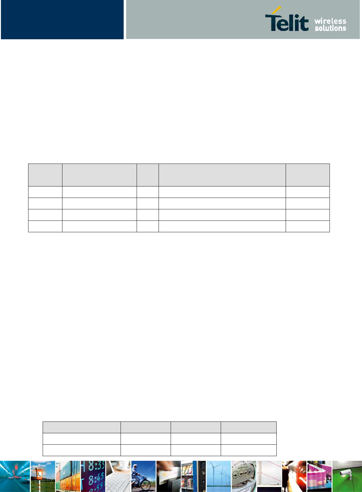
Pin
Number Name I/O Description Level
36 PCM_CLOCK I/O PCM_CLOCK CMOS 2.8V
63 TGPIO_10/PCM_TX I/O TGPIO10 Configurable GPIO/PCM_TX CMOS 2.8V
65 TGPIO_18/PCM_RX I/O TGPIO18 Configurable GPIO/PCM_RX CMOS 2.8V
71 TGPIO_17/PCM_SYNC I/O TGPIO17 Configurable GPIO/PCM_SYNC CMOS 2.8V
9. Miscellaneous signals
9.1. VAUX1
A regulated power supply output is provided in order to supply small devices from module. This
output is active when the module is ON and goes off when module is shut down. The operating
range characteristics of the supply are:
Operating Range – Vout power supply
Parameters Min Typ Max
Output voltage 2.75V 2.85V 2.95V
Output current 100mA
Telit CC864-Dual Hardware user manual
80pppSTzzzzza Rev. 0 , 12-Nov-07
Reproduction forbidden without Telit wireless Solutions – All Right reserved Page 36 of 39
Output bypass
capacitor
2.2uF
Care must be taken to avoid latch-up on the CC864-Dual and the use of this output line to power
electronic devices shall be considered with care, especially for devices that generate spikes and
noise such as level translators, digital ICs or microcontroller, failure in any of these condition can
severely compromise the CC864-Dual functionality.
9.2. VRTC
This pin is used to supply power to RTC(Real Time Clock) Module when CC864-Dual is off state.
RTC module can power up CC864-Dual at alarm time. Refer the “TGPIO_06/ALARM” part.
Connect Super capacitor at this pin. Super capacitor is charged when CC864-Dual is on and it
supply power to the RTC Module when CC864-Dual is off.
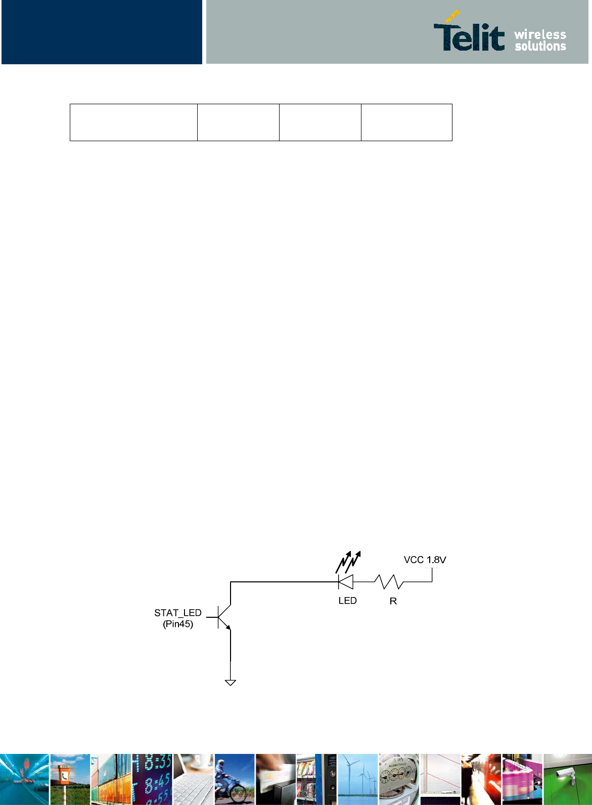
9.3. STAT_LED
This pin is a open collector output signal. It can be synchronized by Slot Cycle Index to make the
LED blinking. Turn On time is 50ms. If the modem is in no service area, the modem turns off the
LED. The LED is blinking in idle mode, and keeps Turn On in traffic mode.

Telit CC864-Dual Hardware user manual
80pppSTzzzzza Rev. 0 , 12-Nov-07
Reproduction forbidden without Telit wireless Solutions – All Right reserved Page 37 of 39
9.4. PWRMON
Its function is similar to ACTIVE. If the reset procedure or boot sequence is finished successfully,
PWRMON will be changed to High state.
9.5. AUDIO_AUX
This pin can be used for Handfree(earphone detection) switching. If the earphone is inserted to the
earjack connector, CC864-Dual will change the audio path to MIC_HF± and EAR_HF± from
MIC_MT± and EAR_MT±.

Telit CC864-Dual Hardware user manual
80pppSTzzzzza Rev. 0 , 12-Nov-07
Reproduction forbidden without Telit wireless Solutions – All Right reserved Page 38 of 39
10. Safety Recommendations
READ CAREFULLY
Be sure the use of this product is allowed in the country and in the environment required. The use
of this product may be dangerous and has to be avoided in the following areas :
Where it can interface with other electronic devices in environments such as hospitals, airports, air
crafts, etc
Where there is risk of explosion such as gasoline, oil refineries, etc
It is responsibility of the user to enforce the country regulation and the specific environment
regulation.
Do not disassemble the product; any mark of tampering will compromise the warranty validity.
We recommend following the instructions of the hardware user guides for a correct wiring of the
product. The product has to be supplied with a stabilized voltage source and the wiring has to be
conforming to the security and fire prevention regulations.
The product has to be handled with care, avoiding any contact with the pins because electrostatic
discharges may damage the product itself. Same cautions have to be taken for the R-UIM card,
checking carefully the instruction for its use. Do not insert or remove the R-UIM when the product
is in power saving mode.
The system integrator is responsible of the functioning of the final product; therefore, care has to
be taken to the external components of the module, as well as of any project or installation issue.
Should there be any doubt, please refer to the technical documentation and the regulation in force.
Every module has to be equipped with a proper antenna with specific characteristics. The antenna
has to be installed with care in order to avoid any interface with other electronic devices and has to
quarantine a minimum distance from the body(20Cm). In case of this requirement cannot be
satisfied, the system integrator has to assess the final product against the SAR regulation.

Telit CC864-Dual Hardware user manual
80pppSTzzzzza Rev. 0 , 12-Nov-07
Reproduction forbidden without Telit wireless Solutions – All Right reserved Page 39 of 39
11. Reference
y QSC6055TM, QSC6065TM, QSC6075TM and QSC6085TM Single ChipTM Device Specification
80-VC881-1
y QSC6055TM, QSC6065TM, QSC6075TM and QSC6085TM Qualcomm Single ChipTM User
Guide 80-VC881-3
12. Document Change Log
Revision Date Changes
Draft #0 12-Nov-07 Draft
FCC Compliance Information
This device complies with Part 15 of FCC Rules.
Operation is subject to the following two conditions:
(1) This device may not cause harmful interference, and
(2) This device must accept any interference received.
Including interference that may cause undesired operation.