Telit Communications S p A CC864-DUAL DUAL BAND CDMA/GPS Module User Manual
Telit Communications S.p.A. DUAL BAND CDMA/GPS Module Users Manual
Contents
- 1. User MAnual
- 2. Users Manual
- 3. User Manual
- 4. user manual
Users Manual

CC864-DUAL Hardware User Guide
80pppSTzzzzza Rev. 0.4 - dd/mm/yy

Notice
OEM integrators and installers are instructed that the phrase. This device contains
transmitter FCC ID: RI7CC864-DUAL must be placed on the outside of the host.
Warning: Exposure to Radio Frequency Radiation The radiated output
power of this device is far below the FCC radio frequency exposure
limits. Nevertheless, the device should be used in such a manner that
the potential for human contact during normal operation is minimized.
In order to avoid the possibility of exceeding the FCC radio
frequency exposure limits, human proximity to the antenna should
not be less than 20cm during normal operation. The gain of the
antenna for Cellular band must not exceed-2.0 dBi.
The gain of the antenna for PCS band must not exceed -3.0dBi.

CC864-DUAL Hardware User Guide
80pppSTzzzzza Rev. 0.4 - dd/mm/yy
Reproduction forbidden without Telit Communications S.p.A’s. written authorization - All Rights Reserved. Page 2 of 49
Disclaimer
The information contained in this document is the proprietary information of Telit
Communications S.p.A. and its affiliates (“TELIT”).
The contents are confidential and any disclosure to persons other than the officers,
employees, agents or subcontractors of the owner or licensee of this document,
without the prior written consent of Telit, is strictly prohibited.
Telit makes every effort to ensure the quality of the information it makes available.
Notwithstanding the foregoing, Telit does not make any warranty as to the
information contained herein, and does not accept any liability for any injury, loss or
damage of any kind incurred by use of or reliance upon the information.
Telit disclaims any and all responsibility for the application of the devices
characterized in this document, and notes that the application of the device must
comply with the safety standards of the applicable country, and where applicable,
with the relevant wiring rules.
Telit reserves the right to make modifications, additions and deletions to this
document due to typographical errors, inaccurate information, or improvements to
programs and/or equipment at any time and without notice.
Such changes will, nevertheless be incorporated into new editions of this document.
All rights reserved.
© 2007 Telit Communications S.p.A.
Printed in the US

CC864-DUAL Hardware User Guide
80pppSTzzzzza Rev. 0.4 - dd/mm/yy
Reproduction forbidden without Telit Communications S.p.A’s. written authorization - All Rights Reserved. Page 3 of 49
Contents
1. Introduction ................................................................................................................... 6
1.1. Scope ....................................................................................................................... 6
1.2. Audience .................................................................................................................. 6
1.3. Contact Information, Support ................................................................................... 6
1.4. Product Overview ..................................................................................................... 6
1.4.1. General Specifications .................................................................................................. 6
1.4.2. Receiver Specifications ................................................................................................. 7
1.4.3. Transmitter Specifications ............................................................................................. 7
1.4.4. gpsOne Receiver Specifications ................................................................................... 7
1.5. Safety Recommendations ........................................................................................ 7
1.5.1. Local regulations ........................................................................................................... 7
1.5.2. Wiring and Installation ................................................................................................... 8
1.5.3. Electrostatic Discharge .................................................................................................. 8
1.5.4. R-UIM Card ................................................................................................................... 8
1.5.5. Antennas ....................................................................................................................... 8
1.5.6. Disassembly .................................................................................................................. 8
1.6. Document Organization ........................................................................................... 8
1.7. Text Conventions ..................................................................................................... 9
1.8. Related Documents .................................................................................................. 9
1.9. Document History ..................................................................................................... 9
2. Mechanical Specifications ......................................................................................... 10
2.1. Module Dimensions ................................................................................................ 10
2.2. Interface Connector Specifications ......................................................................... 11
2.3. RF Connector Specifications .................................................................................. 12
2.4. Mounting ................................................................................................................ 13
3. Hardware Interface Description ................................................................................. 14
3.1. Overview ................................................................................................................ 14
3.2. Functions for Turning On and Off the Module ........................................................ 15
3.2.1. Turning On the CC864-Dual Module ........................................................................... 15
3.2.2. Turning Off the CC864-Dual Module ........................................................................... 16
3.2.2.1. Hardware Shutdown ............................................................................................. 16
3.2.2.2. Software Shutdown .............................................................................................. 16
3.2.3. Hardware Reset .......................................................................................................... 16

CC864-DUAL Hardware User Guide
80pppSTzzzzza Rev. 0.4 - dd/mm/yy
Reproduction forbidden without Telit Communications S.p.A’s. written authorization - All Rights Reserved. Page 4 of 49
3.3. Power Supply ......................................................................................................... 17
3.3.1. +5V Input Source Power Supply Design Guidelines ................................................... 18
3.3.2. +12V Input Source Power Supply Design Guidelines ................................................. 18
3.3.3. Battery Source Power Supply Design Guidelines ....................................................... 19
3.3.4. Battery Charge Control Circuitry Design Guideline ..................................................... 20
3.3.4.1. Trickle Charging ................................................................................................... 21
3.3.4.2. Constant Current Charging .................................................................................. 22
3.3.4.3. Constant Voltage Charging .................................................................................. 22
3.3.4.4. Pulse Charging ..................................................................................................... 22
3.3.5. Thermal Design Guidelines ......................................................................................... 23
3.3.6. Power Supply PCB Layout Guidelines ........................................................................ 23
3.4. Antenna Requirements .......................................................................................... 25
3.4.1. Antenna Installation Guideline ..................................................................................... 25
3.5. Logic level Specification ......................................................................................... 25
3.6. UART1 - Serial Interfaces ...................................................................................... 26
3.6.1. RS232C Interface and Level Translation .................................................................... 27
3.6.2. 5V UART Level Translation ......................................................................................... 28
3.7. External R-UIM Interface ........................................................................................ 29
3.7.1. R-UIM Design Guidelines ............................................................................................ 29
3.8. USB Interface ......................................................................................................... 30
3.9. Audio Interface ....................................................................................................... 30
3.9.1. General Design Rules ................................................................................................. 31
3.9.2. Handset Interface ........................................................................................................ 31
3.9.3. Headset Interface ........................................................................................................ 32
3.9.4. Car Kit Speakerphone Interface .................................................................................. 33
3.10. I2C Bus Interface ................................................................................................ 35
3.11. ADC/DAC Interface ............................................................................................. 35
3.11.1. ADC Converter ........................................................................................................ 35
3.11.1.1. Description ........................................................................................................... 35
3.11.1.2. Using ADC Converter ........................................................................................... 36
3.11.2. DAC Converter ........................................................................................................ 36
3.11.2.1. Description ........................................................................................................... 36
3.11.2.2. Enabling the DAC ................................................................................................. 36
3.11.2.3. Low Pass Filter Example ...................................................................................... 37
3.12. General Purpose I/O ........................................................................................... 37
3.12.1. Using a GPIO pin as Input ....................................................................................... 38
3.12.2. Using a GPIO pin as Output .................................................................................... 38
3.12.3. TGPIO_03/AUDIO MUTE ........................................................................................ 38

CC864-DUAL Hardware User Guide
80pppSTzzzzza Rev. 0.4 - dd/mm/yy
Reproduction forbidden without Telit Communications S.p.A’s. written authorization - All Rights Reserved. Page 5 of 49
3.12.4. TGPIO_04/RF Transmission Control ....................................................................... 38
3.12.5. TGPIO_05/RFTXMON ............................................................................................. 38
3.12.6. TGPIO_06/ALARM .................................................................................................. 39
3.12.7. TGPIO_07/BUZZER ................................................................................................ 39
3.12.8. TGPIO_08/POWER_SAVING ................................................................................. 40
3.12.9. TGPIO_11/VIBRATOR ............................................................................................ 40
3.12.10. TGPIO_12/CALL_KEY ............................................................................................ 40
3.12.11. TGPIO_13/ACTIVE .................................................................................................. 40
3.13. Miscellaneous Interface Signals ......................................................................... 41
3.13.1. VAUX1 ..................................................................................................................... 41
3.13.2. VRTC ....................................................................................................................... 41
3.13.3. STAT_LED ............................................................................................................... 42
3.13.4. PWRMON ................................................................................................................ 42
3.13.5. AXE .......................................................................................................................... 42
4. Development and Testing .......................................................................................... 44
5. Acronyms and Abbreviations .................................................................................... 45
6. Appendix: Pin Allocation ........................................................................................... 46
CC864-DUAL Hardware User Guide
80pppSTzzzzza Rev. 0.4 - dd/mm/yy
Reproduction forbidden without Telit Communications S.p.A’s. written authorization - All Rights Reserved. Page 6 of 49
1. Introduction
1.1. Scope
This document describes hardware solutions you can use to develop a product
containing the Telit CC864-Dual module, as follows:
• Describing the basic functions of the module
• Suggesting a proper hardware solution for each function
• Describing the wrong solutions and most common errors to be avoided
This document is not intended to provide an overall description of all hardware
solutions and all the products that may be designed.
The solutions suggested serve as a guide or starting point for you to be able to
correctly develop a product with the Telit CC864-Dual module.
However, avoiding the wrong solutions and most common errors described here
should be regarded as mandatory.
1.2. Audience
This manual is intended for hardware developers who design products that integrate
the CC864-DUAL module.
1.3. Contact Information, Support
For detailed information about where you can buy the Telit modules or for
recommendations on accessories and components visit http://www.telit.com
To register for product news and announcements or for product questions contact
Telit's Technical Support Center (TTSC).
1.4. Product Overview
The CC864-Dual module is a CDMA-1XRTT wireless module designed to have the
same form, fit and function as its GSM/GPRS counterpart product family, the GC864-
Dual.
This enables integrators and developers to design their applications once and take
advantage of the global coverage and service flexibility allowed by the combination of
the most prevalent cellular technologies worldwide.
With its ultra-compact design and extended operating temperature range, the Telit
CC864-Dual module is the perfect platform for m2m applications, mobile data and
computing devices. It also incorporates gpsOne capability for applications in mobile
environments such as telematics, personal and asset tracking.
1.4.1. General Specifications
Parameter Description
External access Code division multiple access
CC864-DUAL Hardware User Guide
80pppSTzzzzza Rev. 0.4 - dd/mm/yy
Reproduction forbidden without Telit Communications S.p.A’s. written authorization - All Rights Reserved. Page 7 of 49
CDMA protocol CDMA2000 1x Rel A and Rel B
Data Rate 153.6 Kb/s (full-duplex)
GPS SGPS / standalone
Vocoder EVRC, 13kQCELP, 4GV
Operating temperature -30° ~ +80°
1.4.2. Receiver Specifications
Parameters Descriptions
Frequency range Cellular: 869~894 MHz
PCS: 1930~1990 MHz
Channel number Cellular: 832
PCS: 1200
Sensitivity Better than -104 dBm
Input dynamic range -25dBm ~ -104 dBm
1.4.3. Transmitter Specifications
Parameters Descriptions
Frequency range Cellular: 824~849 MHz
PCS: 1850~1910 MHz
Channel number Cellular: 832
PCS: 1200
Power class Cellular: Class III
PCS: Class II
Power range 0.2 W (23 dBm) ~ 0.63 W (28 dBm)
Nominal power 0.27 W (24.31 dBm)
1.4.4. gpsOne Receiver Specifications
Parameters Descriptions
Frequency range L1, 1575.42 MHz
Receiver sensitivity -151 dBm
1.5. Safety Recommendations
1.5.1. Local regulations
Make sure that the use of this product is allowed in the country and in the
environment required.
The use of this product may be dangerous and thus must be avoided where:

CC864-DUAL Hardware User Guide
80pppSTzzzzza Rev. 0.4 - dd/mm/yy
Reproduction forbidden without Telit Communications S.p.A’s. written authorization - All Rights Reserved. Page 8 of 49
• It can interface with other electronic devices in environments such as
hospitals, airports, and so on.
• There is risk of explosion such as in the proximity of gasoline, oil refineries,
and so on.
You are responsible to enforce country and specific environment regulations on the
product. For further details refer to Chapter 1.7 for related documents.
1.5.2. Wiring and Installation
Always follow the instructions of this guide when wiring the product.
The product must be supplied with a stabilized voltage source, and the wiring must
conform to security and fire prevention regulations.
The installation of the external components of the module must be handled with care
in order to ensure the proper functioning of the product.
1.5.3. Electrostatic Discharge
The product must be handled with care, avoiding any contact with the pins because
electrostatic discharge can damage the product.
1.5.4. R-UIM Card
The R-UIM card must also be handled with care, always following the instructions for
its use.
Do not insert or remove the R-UIM when the product is in power saving mode.
1.5.5. Antennas
Every module must be equipped with a proper antenna with specific characteristics.
The antenna must be installed with care in order to avoid any interference with other
electronic devices, and it must also have a minimum distance of 20 cm from the body.
In case this requirement cannot be satisfied, the system integrator must assess the
final product against the applicable SAR regulations.
1.5.6. Disassembly
Do not disassemble the product.
Any evidence of tampering will void the warranty.
1.6. Document Organization
This manual contains the following chapters:
“Chapter 1: Introduction” provides a scope for this manual, target audience, contact
and support information, and text conventions.
CC864-DUAL Hardware User Guide
80pppSTzzzzza Rev. 0.4 - dd/mm/yy
Reproduction forbidden without Telit Communications S.p.A’s. written authorization - All Rights Reserved. Page 9 of 49
“Chapter 2: Mechanical Specifications” contains information on the dimensions of the
module, the interface connector and the RF connector, and on how to include the
module into external applications.
“Chapter 3: Hardware Interface Description” describes the hardware interfaces of the
product and provides guidelines for using the module in various applications.
“Chapter 4: Development and Testing” provides information on how to connect the
module to the Telit Evaluation Kit (EVK).
“Chapter 5: Acronyms and Abbreviations” provides definition for all the acronyms and
abbreviations used in this guide.
“Appendix: Pin Allocation” specifies the allocation of the pins on the connector that is
used for connecting the unit with external applications.
1.7. Text Conventions
Danger – This information MUST be followed or catastrophic equipment failure or
bodily injury may occur.
Caution or Warning – Alerts the user to important points about integrating the module,
if these points are not followed, the module and end user equipment may fail or
malfunction.
Tip or Information – Provides advice and suggestions that may be useful when
integrating the module.
1.8. Related Documents
The following documents are related to this user guide:
• CC864-DUAL Product Description – (Doc No)
• CC864-DUAL Software Description – (Doc No)
1.9. Document History
Doc rev # Date Changes Location in
Guide
0.3 01.03.2008 First version for Peer review
0.4 04.03.2008 Updates after review
CC864-DUAL Hardware User Guide
80pppSTzzzzza Rev. 0.4 - dd/mm/yy
Reproduction forbidden without Telit Communications S.p.A’s. written authorization - All Rights Reserved. Page 10 of 49
2. Mechanical Specifications
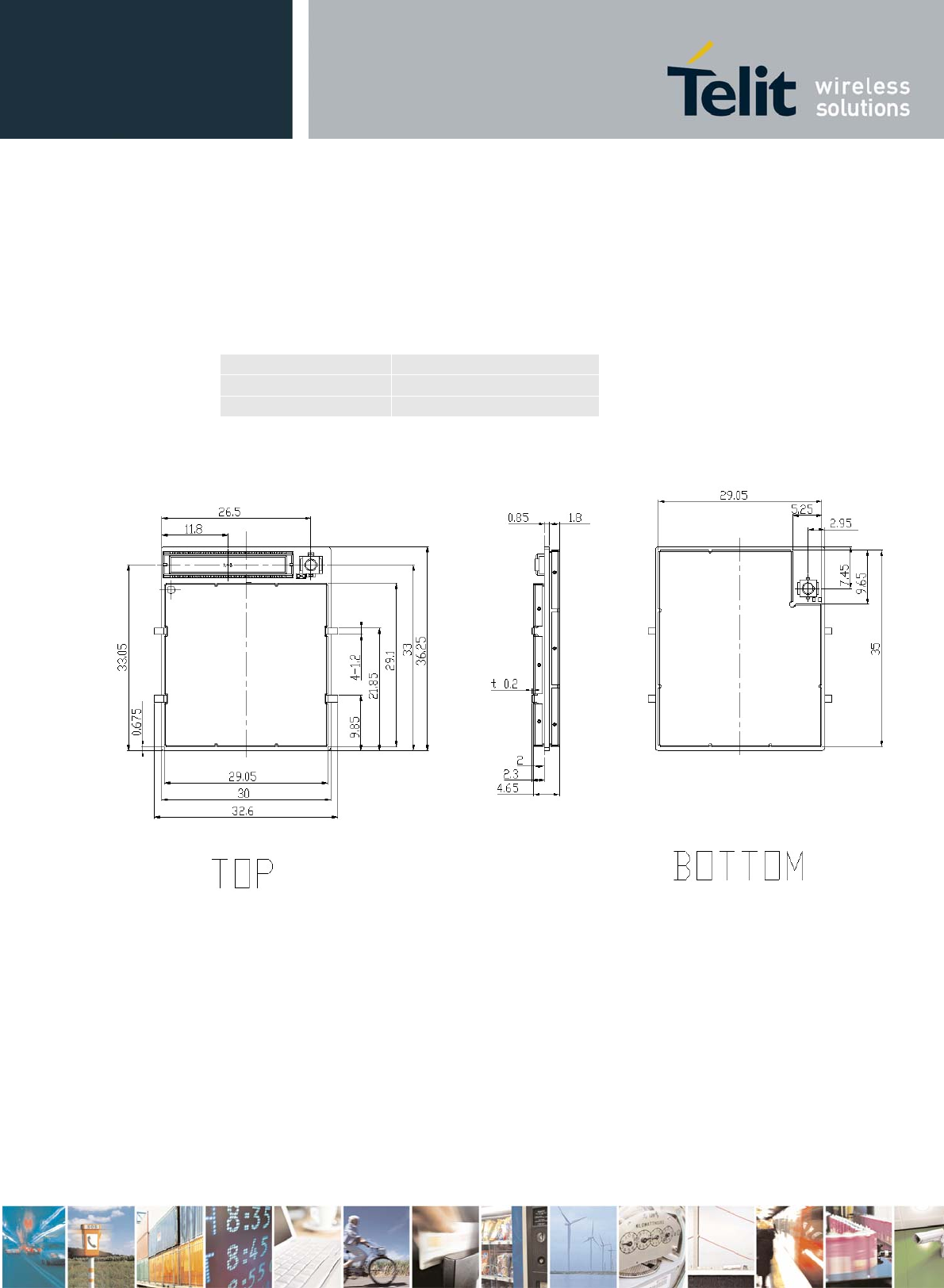
2.1. Module Dimensions
The CC864-DUAL overall dimensions are:
Length: 36.25 mm
Width: 30.00 mm*
Thickness: 4.65 mm*
*) Excluding solder pads.
CC864-DUAL Hardware User Guide
80pppSTzzzzza Rev. 0.4 - dd/mm/yy
Reproduction forbidden without Telit Communications S.p.A’s. written authorization - All Rights Reserved. Page 11 of 49
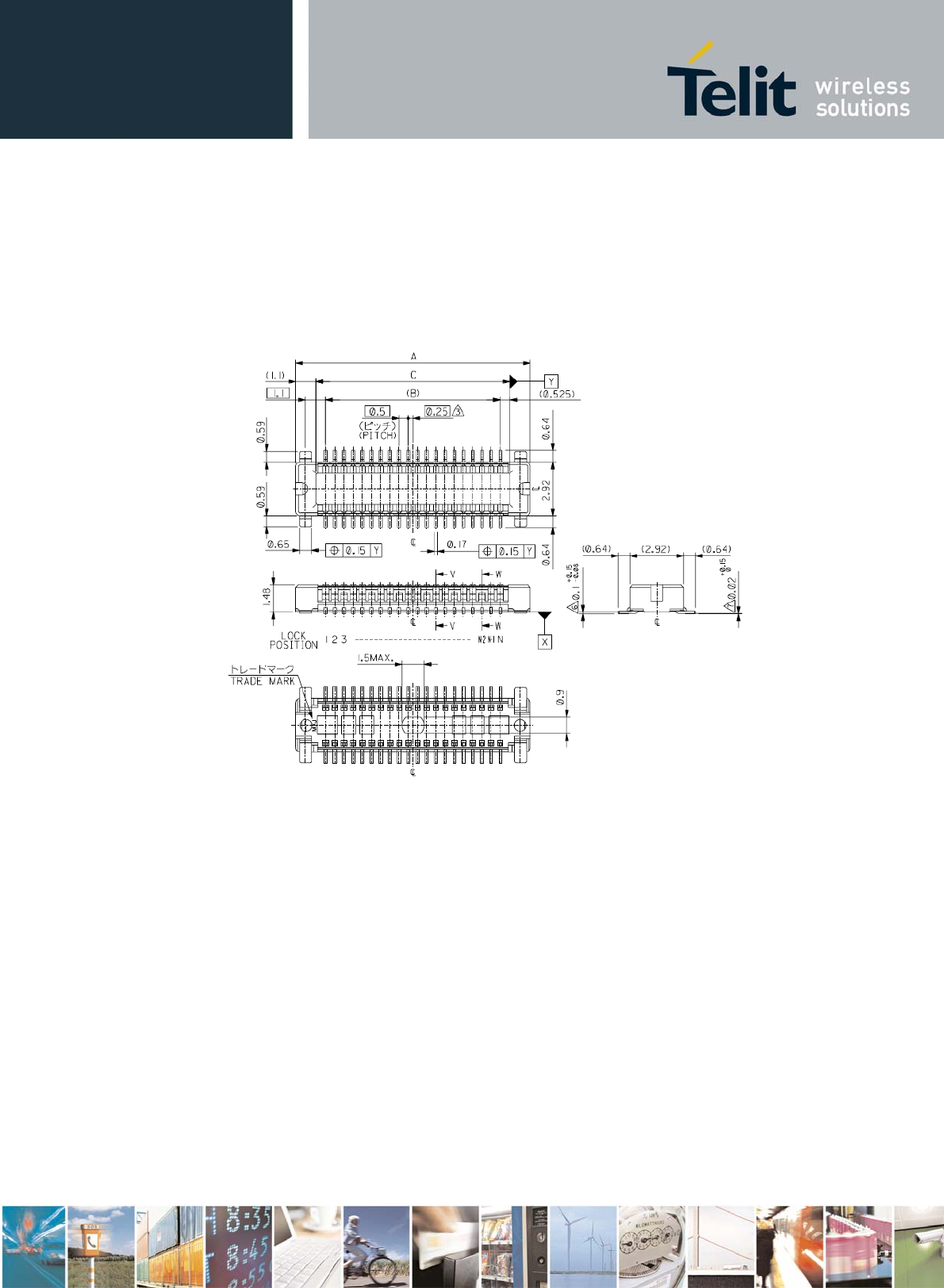
2.2. Interface Connector Specifications
The CC864-Dual module is equipped with a Molex 80-pin board-to-board connector
and P/N 0539490878 (male).
The mating part is Molex P/N 0541500878 (female).
CC864-DUAL Hardware User Guide
80pppSTzzzzza Rev. 0.4 - dd/mm/yy
Reproduction forbidden without Telit Communications S.p.A’s. written authorization - All Rights Reserved. Page 12 of 49
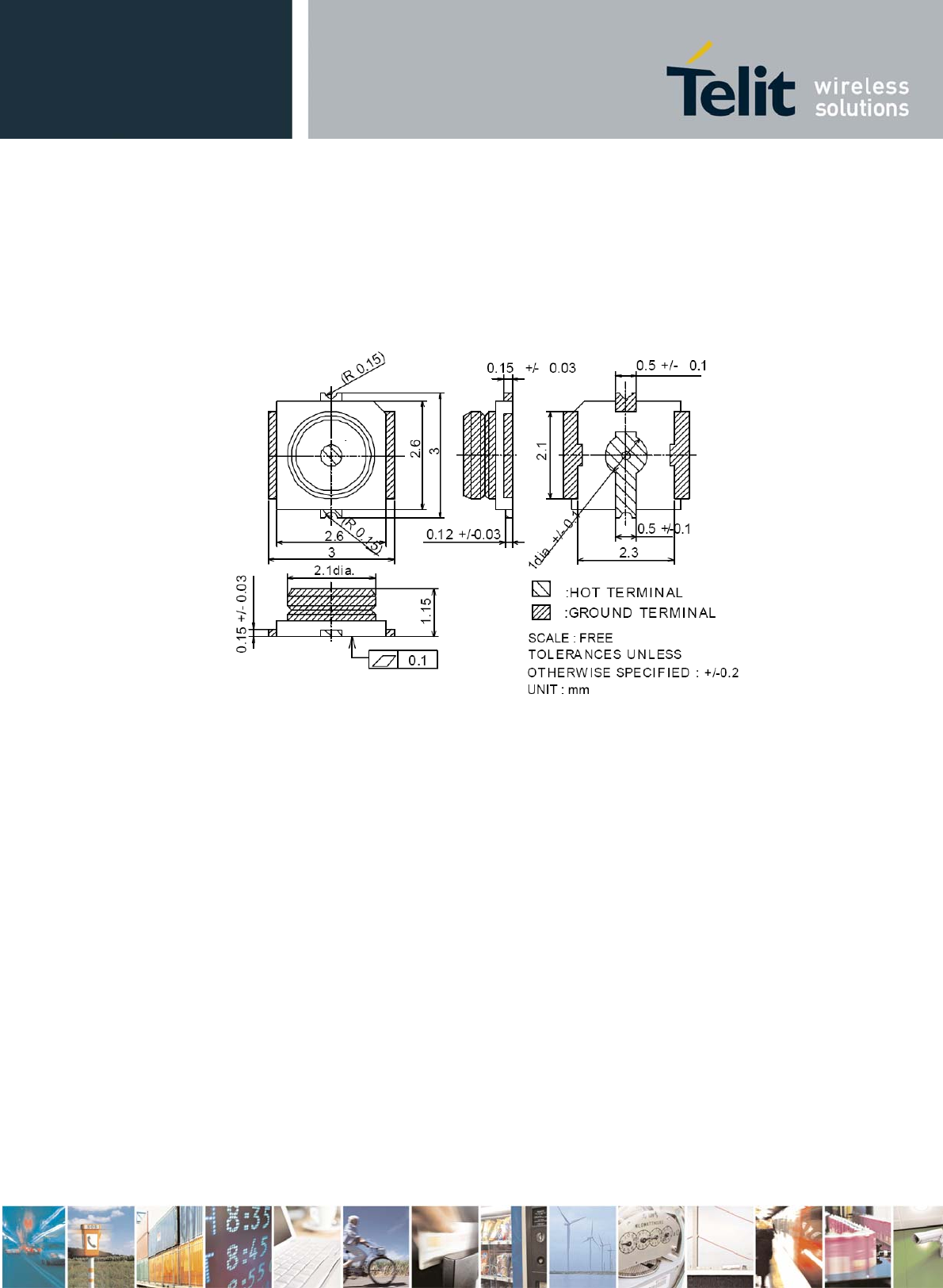
2.3. RF Connector Specifications
The CC864-Dual module is equipped with a Murata GSC type 50 Ohm RF connector,
and P/N MM9329-2700.
The suitable counterpart is Murata MXTK92 type or MXTK88 type connector.
CC864-DUAL Hardware User Guide
80pppSTzzzzza Rev. 0.4 - dd/mm/yy
Reproduction forbidden without Telit Communications S.p.A’s. written authorization - All Rights Reserved. Page 13 of 49
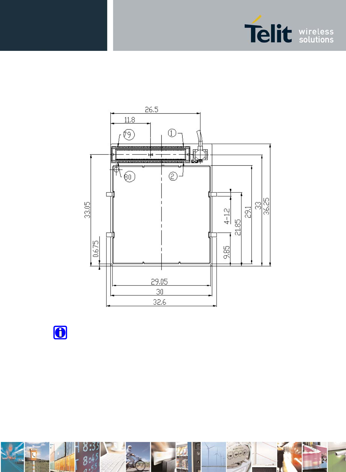
Mounting
The figure below shows the position of the Molex board-to-board connector and pin 1.
Tip: It is highly recommended to maintain a 1.5mm clearance from all wireless
modems to any components, including around the solder tabs.
CC864-DUAL Hardware User Guide
80pppSTzzzzza Rev. 0.4 - dd/mm/yy
Reproduction forbidden without Telit Communications S.p.A’s. written authorization - All Rights Reserved. Page 14 of 49
3. Hardware Interface Description
3.1. Overview
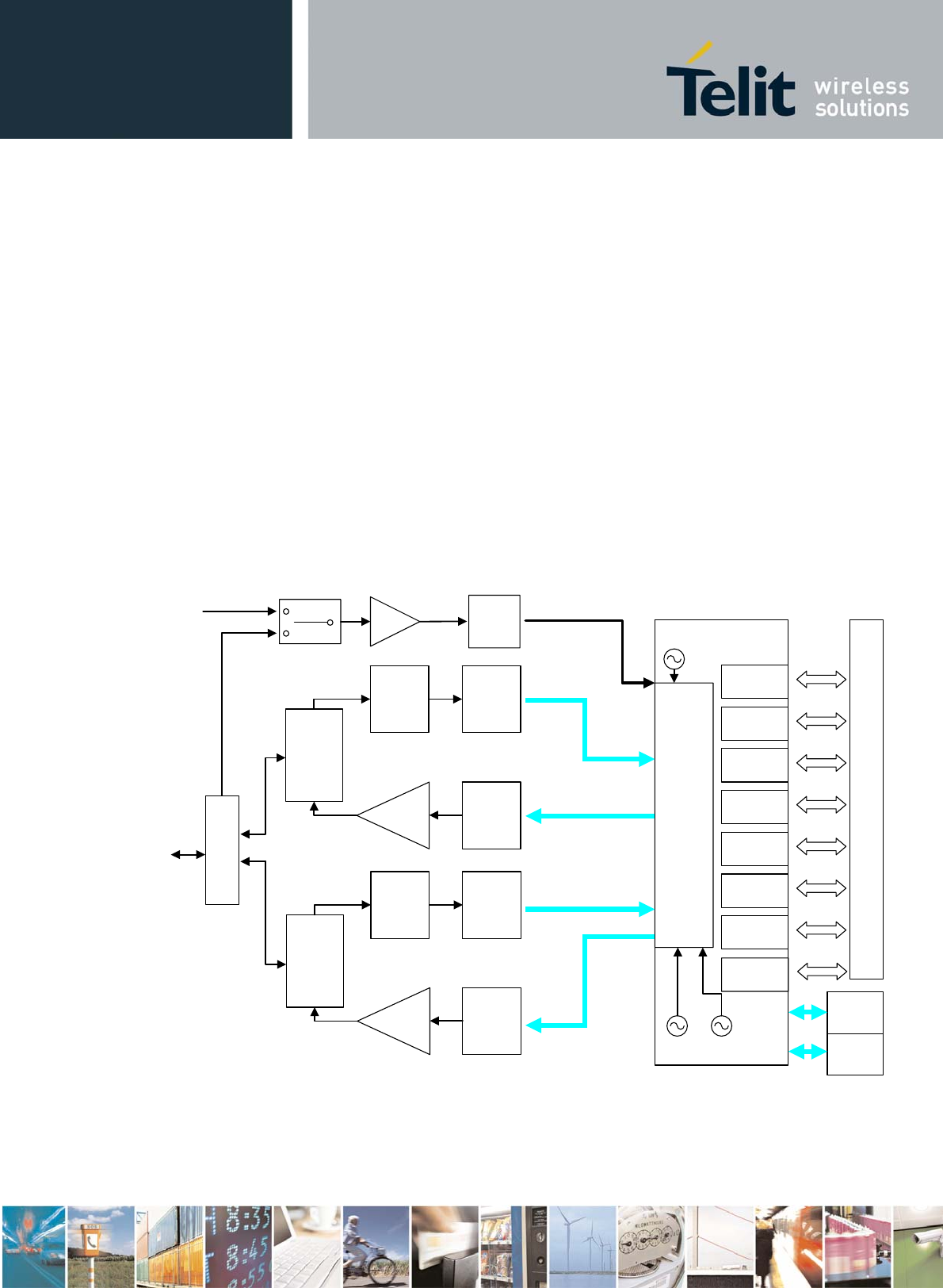
The CC864-Dual module has the following main interface function blocks:
• UART1 (used for AT commands)
• USB (used for diagnostic monitoring)
• R-UIM (UART2)
• GPIOs
• Audio (includes Analog I/O audio codecs and PCM interface)
• JTAG
• Miscellaneous pins (including I2C)
To
Antenna
QSC 6055
80 Pin Modem Interface Connector
RF Interface
US-PCS
Duplexer
RX
Filter
US
PCS
LNA
PAM TX
Filter
Cellular
Duplexer
RX
Filter
Cellular
LNA
PAM TX
Filter
Triplexer
USB
UART1
RUIM
GPIOs
CODEC
JTAG
Misc
To GPS
Dedicated
Antenna
ROM
RAM
CDMA Rx GPS
CDMA Tx
IIC
GPS
filter
LNA
GPS
Switch

CC864-DUAL Hardware User Guide
80pppSTzzzzza Rev. 0.4 - dd/mm/yy
Reproduction forbidden without Telit Communications S.p.A’s. written authorization - All Rights Reserved. Page 15 of 49
3.2. Functions for Turning On and Off the Module
3.2.1. Turning On the CC864-Dual Module
To turn on the module the ON/OFF Pin must be tied for at least one second, and
then released.
A Few Examples
1) Let's assume you need to drive the ON_OFF pin with a totem pole output of a +3/5
V microcontroller (uP_OUT1):
1s
CC864-DUAL Hardware User Guide
80pppSTzzzzza Rev. 0.4 - dd/mm/yy
Reproduction forbidden without Telit Communications S.p.A’s. written authorization - All Rights Reserved. Page 16 of 49
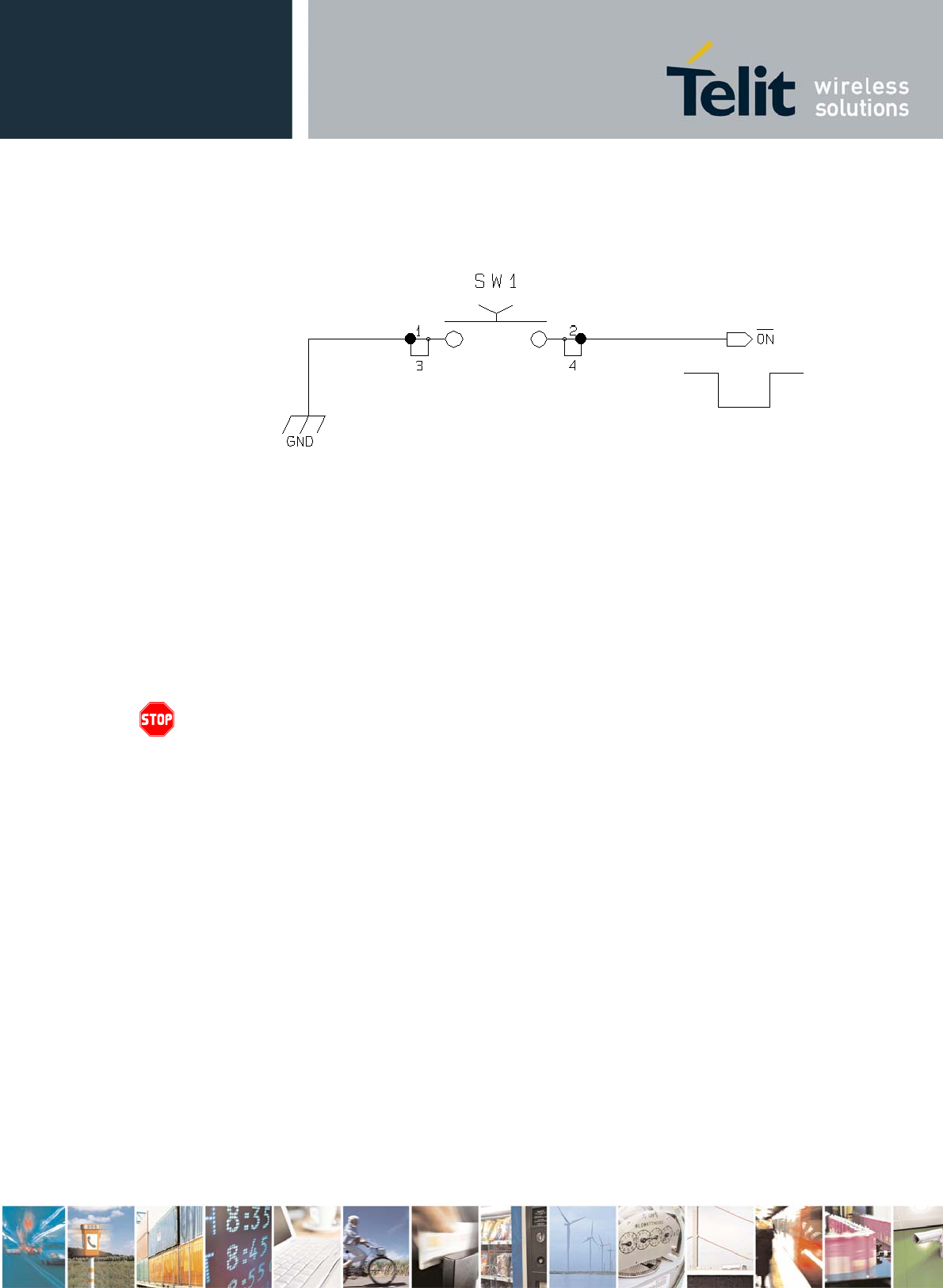
2) Let's assume you need to drive the ON_OFF pin directly with an ON/OFF
button:
3.2.2. Turning Off the CC864-Dual Module
You can turn off the device with either a software command or a hardware shutdown
circuit.
When the device is shut down either way, it issues to the network a detach request
with the information that the device is not reachable any more.
Warning: Never disconnect power before the power off procedure is completed. If
you do, this may cause severe damage the module primarily due to the possibility of
memory corruption that renders the module inoperable.
3.2.2.1. Hardware Shutdown
To turn off the CC864-Dual module the ON/OFF Pin must be tied for at least one
second, and then released.
The same circuitry and timing as for power on must be used for be used for powering
off the module.
The device shuts down after you release the ON_OFF Pin.
3.2.2.2. Software Shutdown
Please refer the “Software User Guide” for information on how to shut down the
module using AT-commands.
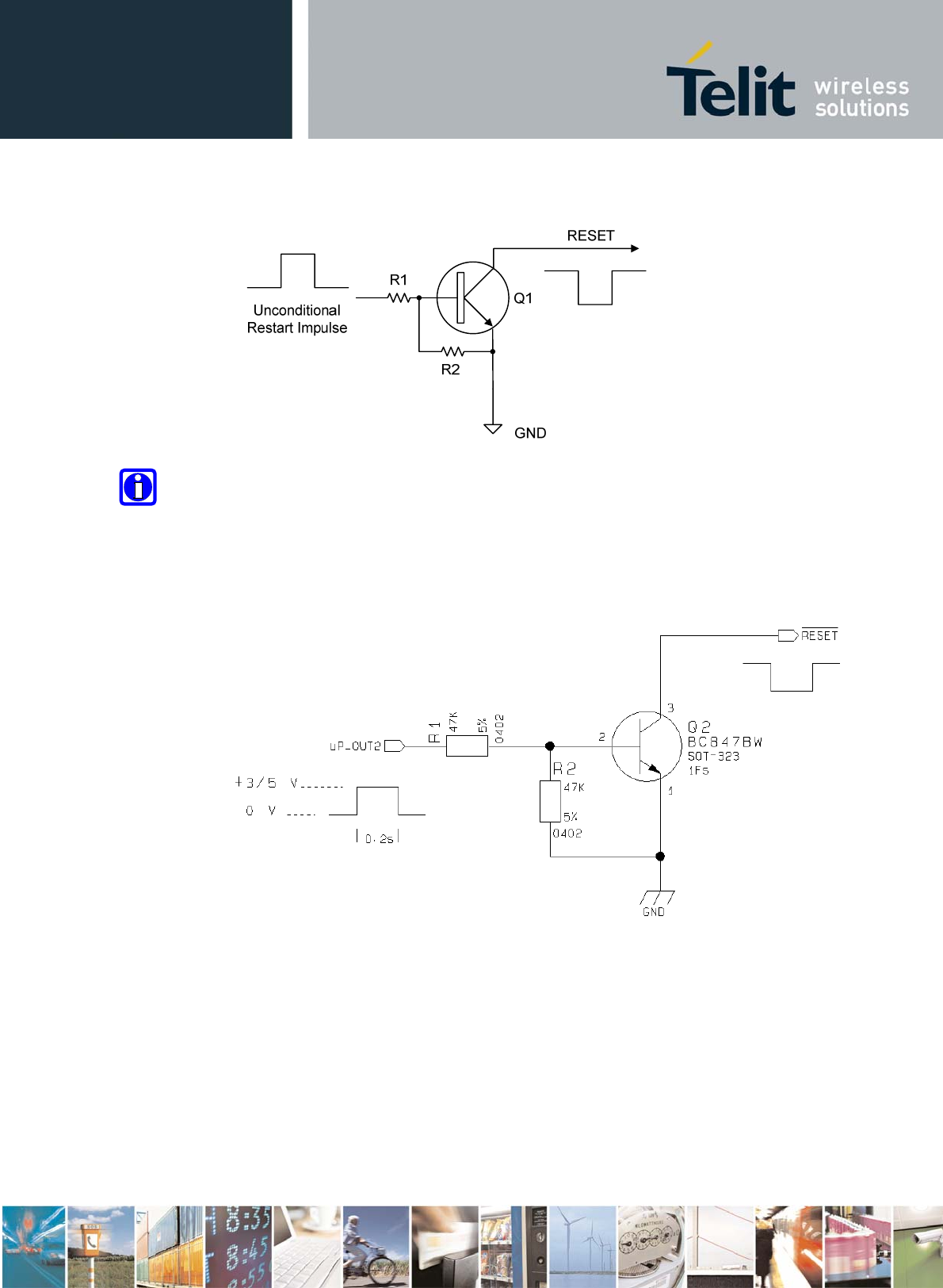
3.2.3. Hardware Reset
To perform hardware reset and reboot the module, the RESET pin must be tied low
for at least 200 milliseconds, and then released.
CC864-DUAL Hardware User Guide
80pppSTzzzzza Rev. 0.4 - dd/mm/yy
Reproduction forbidden without Telit Communications S.p.A’s. written authorization - All Rights Reserved. Page 17 of 49
The following figure shows a sample circuit to accomplish this operation:
TIP: A hardware reset circuit should be always implemented on the host board but
the host should use it as an emergency reset procedure only.
Example
Let's assume you need to drive the RESET# pad with a totem pole output of a +3/5 V
microcontroller (uP_OUT2):
3.3. Power Supply
The electrical design of the power supply strongly depends on the power source from
which the power is drained. We will discuss the following three common categories:
• +5V input source supply (typically PC internal regulator output)
• +12V input source supply (typically automotive)
• Battery source supply

CC864-DUAL Hardware User Guide
80pppSTzzzzza Rev. 0.4 - dd/mm/yy
Reproduction forbidden without Telit Communications S.p.A’s. written authorization - All Rights Reserved. Page 18 of 49
3.3.1. +5V Input Source Power Supply Design Guidelines
The desired output for the power supply is 3.8V, hence there’s not a big difference
between the input source and the desired output and a linear regulator can be used. .
When using a linear regulator, a proper heat sink may be required in order to
dissipate the heat.
A bypass low ESR capacitor of adequate capacity must be provided in order to cut
the current absorption peaks close to the CC864-Dual module, a 100µF tantalum (or
equivalent) capacitor is suited for this purpose.
Make sure the low ESR capacitor on the power supply output (usually a tantalum) is
rated at least 10V.
A protection diode should be inserted close to the power input, in order to protect the
module from power polarity inversion.
A typical example of a linear regulator with 5V input is:
3.3.2. +12V Input Source Power Supply Design Guidelines
The desired output for the power supply is 3.8V, and due to the large difference
between the input voltage and the desired output, a linear regulator is not well suited
and should not be used. A switching power supply is preferred because of its better
efficiency with the 2A peak current load drawn by the CC864-Dual module.
When using a switching regulator, a 500 KHz or more switching frequency regulator
is preferable because of its smaller inductor size and faster transient response. This
allows the regulator to respond quickly to current peaks.

CC864-DUAL Hardware User Guide
80pppSTzzzzza Rev. 0.4 - dd/mm/yy
Reproduction forbidden without Telit Communications S.p.A’s. written authorization - All Rights Reserved. Page 19 of 49
In any case the frequency and switching design selection is related to the application
to be developed due to the fact the switching frequency could also generate EMC
interferences and the application must also take this into account.
For a car PB battery the input voltage can rise up to about 16V and when choosing
components, all components in the power supply must withstand this voltage.
Power supplies for automotive use are complicated and have to take a number of
issues into account, such as: over voltage, reverse polarity, cranking, load dump
booster batteries, forced charging etc
A bypass low ESR capacitor of adequate capacity must be provided in order to cut
the current absorption peaks; a 100µF tantalum (or equivalent) capacitor is suitable
for this purpose.
Make sure the low ESR capacitor on the power supply output (usually a tantalum) is
rated at least 10V.
For car applications a spike protection diode must be inserted close to the power
input, in order to clean the supply from spikes and a specific automotive grade
regulator is recommended.
A protection diode (which can be the same diode as in spike protection) must be
inserted close to the power input in order to save the CC864-Dual module from
power polarity inversion.
A typical example of a switching regulator with 12V input is:
3.3.3. Battery Source Power Supply Design Guidelines
The desired nominal output for the power supply is 3.8V and the maximum voltage
allowed is 4.2V, so that a single 3.7V lithium-ion cell battery type is ideal to supply
the power to the module.
Three regular battery cells (Ni/Cd or Ni/MH 3.6V nom. battery types or 4V PB types)
must not be used directly because their maximum voltage can rise over the absolute
maximum voltage for the CC864-Dual module and damage it.
CC864-DUAL Hardware User Guide
80pppSTzzzzza Rev. 0.4 - dd/mm/yy
Reproduction forbidden without Telit Communications S.p.A’s. written authorization - All Rights Reserved. Page 20 of 49
Warning: DO NOT USE any Ni-Cd, Ni-MH or Pb battery types directly connected to
the module! Their use can lead to overvoltage and damage the module. USE ONLY
Li-Ion battery types.
A bypass low (usually a 100uF tantalum) ESR capacitor with adequate capacity must
be provided in order to cut the current absorption peaks. Make sure the low ESR
capacitor (usually a tantalum) is rated at least 10V.A protection diode must be
inserted close to the power input, in order to protect the module from voltage polarity
inversion.
The suggested battery capacity is from 500mAh to 1000mAh.
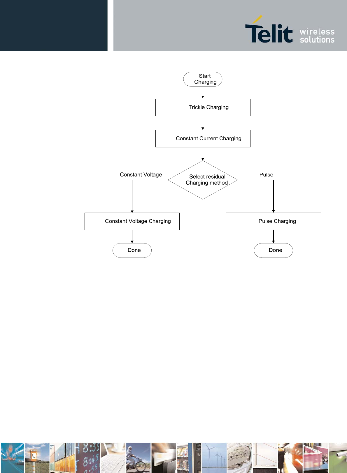
3.3.4. Battery Charge Control Circuitry Design Guideline
The CC864-Dual module provides support circuitry for charging a lithium-ion battery,
utilizing four firmware-controlled charging modes:
• Trickle charging
• Constant current charging
• Constant voltage charging
• Pulsed charging
Battery voltage, external supply voltage, and total detected current measurements
are available to the module firmware through the analog multiplexer, which allow the
module firmware to monitor charging parameters, make decisions, and control the
charging process.
Note: This process is completely transparent to the application and is controlled by
the module firmware; it is described below for completeness and battery selection
purposes only.
• Charging begins with trickle charging, which limits the current and avoids
pulling the VDD down.
• Once a minimum battery voltage is established using trickle charging,
constant current charging is enabled by the firmware in order to charge the
battery quickly (this mode is sometimes called fast charging).
• When the Li-ion battery approaches its target voltage (through constant
current charging), the charge is completed using either constant voltage or
pulse charging.
Further description of all charging modes is provided in the sections below.
The following figure illustrates the main battery charging sequence.
CC864-DUAL Hardware User Guide
80pppSTzzzzza Rev. 0.4 - dd/mm/yy
Reproduction forbidden without Telit Communications S.p.A’s. written authorization - All Rights Reserved. Page 21 of 49
3.3.4.1. Trickle Charging
The module firmware and power management circuitry provides trickle charging of
the main battery when powered from VDD.
This mode is used by the module to raise a severely depleted battery’s voltage to a
level sufficient to begin fast charging.
Attempting fast charging with a high-current supply on a deeply discharged battery,
would cause the battery do draw excessive current, pull the VDD voltage down, and
possibly cause a module malfunction or shutdown due to an under-voltage lockout
condition.
In order to avoid these problems, the module provides a constant, low-current
charging mode: trickle charging.
Trickle charging is used by the module firmware until the main battery reaches a
predefined desired threshold, which is usually about 3.0V for Li-ion batteries.
The threshold varies with battery type and application, so there is no predefined
value implemented in the detection circuits.
The firmware stops the trickle charging based on battery voltage measurements and
battery type.
CC864-DUAL Hardware User Guide
80pppSTzzzzza Rev. 0.4 - dd/mm/yy
Reproduction forbidden without Telit Communications S.p.A’s. written authorization - All Rights Reserved. Page 22 of 49
3.3.4.2. Constant Current Charging
The Module firmware supports constant current charging of the main battery.
During constant current charging the battery is charged with a constant current of
600mA.
As the battery voltage rises and approaches its desired value of 4.2V the charging
current begins to decrease, indicating the end of constant current charging and the
beginning of residual charging.
The charging firmware monitors the voltage and takes the appropriate action to
terminate the constant current charging mode. Charging continues with residual
charging (either constant voltage or pulsed).
Note: In this application the charging firmware limits the charging current to 600mA.
3.3.4.3. Constant Voltage Charging
Once constant current charging of the lithium-ion battery is finished, the charging
continues using either constant voltage or pulsed techniques.
Constant voltage charging is similar to the constant current mode:
The battery voltage is constant while the charging current decreases exponentially
for the remaining charging process.
The end of the constant voltage charging is typically detected by allowing voltage
operation for a pre-determined duration beyond crossing the VBATDET threshold in
the internal charger IC (lasting for one and a half or two hours).
The firmware limits the predetermined duration, not allowing charging to continue
indefinitely, because charging for too long can damage the battery.
3.3.4.4. Pulse Charging
Pulse charging is implemented by switching the pass transistor on the internal
charger IC on and off.
The module and external electronics must draw minimal current so the battery’s open
circuit voltage can be measured accurately during the off interval.
Pulse charging, compared to constant voltage charging:
• Provides better voltage accuracy
• Reaches full charge more quickly
• Dissipates less transistor power when switching from constant current
charging
Pulse charging is enabled through firmware control, and it uses the same hardware
as constant current or constant voltage charging, but repetitiously opens and closes
the pass transistor to deliver current pulses to the battery
One purpose of pulsed operation is to check and recheck the battery’s open circuit
voltage, confirming a full charger before terminating the process.
CC864-DUAL Hardware User Guide
80pppSTzzzzza Rev. 0.4 - dd/mm/yy
Reproduction forbidden without Telit Communications S.p.A’s. written authorization - All Rights Reserved. Page 23 of 49
3.3.5. Thermal Design Guidelines
The thermal design for the module and its power supply needs to take the following
parameters into account:
Average current consumption during transmission at
Max level (23~24dBm) Cellular : 500mA
PCS : 580mA
Average current consumption during transmission at
Min level (-50dBm) Cellular : 130mA
PCS : 140mA
Average current during Idle mode
(when receiver circuit is on, transmitter circuit is off) 100mA
Average current during sleep mode
when receiver/transmitter circuits are off, only baseband
circuit is on)
1mA
Average current during hibernation mode
(All circuits are off except alarm circuit) 2.6uA
NOTE: The average current consumption during transmissions depends on the
power level at which the device is requested to transmit by the network.
Hence, the average current consumption varies significantly.
Considering the very low current during idle and sleep time, especially when the
power saving function is enabled, from a thermal point of view ,it is possible to
estimate that the device only draws significant current during calls.
An Example
If the device stays in transmission for a few minutes and then remains idle for an
hour, the power supply always has the time to cool down between the calls. The heat
sink can then be smaller than the calculated 700mA maximum RMS current, or there
can be no heat sink (simple chip package).
In average network conditions, the device is requested to transmit at a lower power
level than the maximum, and thus the current consumption is less than 700mA.
For these reasons, the thermal design is rarely a concern and the using the ground
plane where the power supply chip is placed as the heat sink can be enough to
ensure good thermal conditions and avoid overheating.
The generated heat is primarily conducted to the ground plane under the module and
the ambient air by convection, so you must ensure that your application can dissipate
the heat as required.
3.3.6. Power Supply PCB Layout Guidelines
Telit recommends that the power supply for the CC864-DUAL module to be designed
to meet the higher demands of a GSM/UMTS module.
The power supply will be slightly over-dimensioned for a CDMA module, but will allow
for the easy transition to another technology, if need be (GSM/UMTS 2A vs. CDMA
1A peak current consumption).

CC864-DUAL Hardware User Guide
80pppSTzzzzza Rev. 0.4 - dd/mm/yy
Reproduction forbidden without Telit Communications S.p.A’s. written authorization - All Rights Reserved. Page 24 of 49
The power supply implementation must have a low ESR capacitor on the output to
smooth the current peaks and should include a protection diode on the power supply
input to protect the supply from spikes and polarity inversion.
The placement of these components is crucial for the correct operation of the circuitry
and application.
A misplaced component can be ineffective or even decrease the power supply
performance:
• The Bypass low ESR capacitor must be placed close to the module power
input pads or in the case the power supply is a switching type it can be placed
close to the inductor to cut the ripple provided the PCB trace from the
capacitor to the module is wide enough to ensure no voltage drops during the
transmission current peaks.
• The protection diode must be placed close to the input connector where the
power source is drained.
• The PCB traces from the input connector to the power regulator IC must be
wide enough to ensure no voltage drops occur during the transmission
current peaks.
(GSM/UMTS specific consideration) Note that this is not made in order to
save power loss but especially to avoid the voltage drops on the power line at
the current peaks frequency of 216 Hz that will reflect on all the components
connected to that supply, introducing a noise floor at the burst base frequency.
For this reason, while a voltage drop of 300-400 mV may be acceptable from
the power loss point of view, the same voltage drop may not be acceptable
from the noise point of view.
If your application doesn't have audio interface but only uses the data feature
of the GSM /UMTS Wireless Modem, then this noise may not be so disturbing
and power supply layout design can be more forgiving.
• The PCB traces to module and the Bypass capacitor must be wide enough to
ensure no significant voltage drops occur during the GSM 2A/CDMA 1A
current peaks.
This is for the same reason as the previous point. Try to keep this trace as
short as possible.
• The PCB traces connecting the Switching output to the inductor and the
switching diode must be kept as short as possible by placing the inductor and
the diode very close to the power switching IC (only for switching power
supply). This is done in order to reduce the radiated field (noise) at the
switching frequency (usually 100-500 kHz).
• The use of a good common ground plane is suggested.
• The placement of the power supply on the board should be done in such a
way to guarantee that the high current return paths in the ground plane are
not overlapped to any noise sensitive circuitry as the microphone
amplifier/buffer or earphone amplifier.
The power supply input cables/traces should be kept separate from noise sensitive
lines such as microphone/earphone cables/traces.
CC864-DUAL Hardware User Guide
80pppSTzzzzza Rev. 0.4 - dd/mm/yy
Reproduction forbidden without Telit Communications S.p.A’s. written authorization - All Rights Reserved. Page 25 of 49
3.4. Antenna Requirements
Parameter Descriptions
Frequency range (CDMA) Tx: 824MHz ~ 849Mhz,
Rx: 869Mhz ~ 894MHz
Frequency range (PCS) Tx: 1850MHz ~ 1910MHz,
Rx: 1930MHz ~ 1990MHz
Frequency range (GPS) 1575.42MHz
Impedance 50 Ohm
Recommended VSWR < 2
Radiation pattern Omni-directional
Polarization Vertical
Note: if the device is developed for the US and/or Canadian market, it must comply
with the FCC and/or IC approval requirements.
3.4.1. Antenna Installation Guideline
Install the antenna in a place covered by the CDMA signal.
The antenna must be installed to provide a separation distance of at least 20 cm from
all persons and must not be co-located or operating in conjunction with any other
antenna or transmitter.
The antenna must be installed according to the antenna manufacturer instructions.
Warning: The antenna must not be installed inside metal cases.
3.5. Logic level Specification
The CC864-Dual module serial port is the core of the interface between the module
and the host hardware.
Depending on the serial port type of the host hardware, a level translator circuit may
be needed for the system to function properly. The only configuration that does not
need a level translation is interfacing to a 2.8V UART.
On the CC864-Dual module there are two UART ports, one is for UART1 and the
other is for R-UIM/UART2. It differs from the standard PC RS232C in signal polarity
(where RS232 is reversed) and in levels.
Where not specifically stated, the interface circuits work at 2.8V CMOS logic levels.
The following tables show the logic level specifications for the CC864-Dual module
interface circuits:
Operating Range – Interface levels (2.8V CMOS)
CC864-DUAL Hardware User Guide
80pppSTzzzzza Rev. 0.4 - dd/mm/yy
Reproduction forbidden without Telit Communications S.p.A’s. written authorization - All Rights Reserved. Page 26 of 49
Parameter Min Max
VIH (input high level) 1.76 V 3.0 V
VIL (input low level) -0.3 V 0.95 V
VOH (output high level) 2.25 V 2.7 V
VOL (output low level) 0.0 V 0.45 V
Operating Range – Interface levels (1.8V CMOS)
Parameter Min Max
VIH (input high level) 1.2V 2.1V
VIL (input low level) -0.3V 0.63V
VOH (output high level) 1.35V 1.8V
VOL (output low level) 0.0V 0.45V
3.6. UART1 - Serial Interfaces
The CC864-Dual module is capable of providing up to two universal asynchronous
(UART) ports.
The UART can also be used as the module’s serial data port for test and debug, and
can support additional interface functions such as an external keypad or ringer.
The UART1 can also be used to load and/or upgrade system firmware (in addition to
the USB port).
Default setting is UART1 for the AT-commands and UART2 for R-UIM
The following table lists the signals of the CC864-Dual module serial port:
RS232
Pin Nr Signal PIN
Number Name Usage
1 C109/DCD 32 Data Carrier
Detect
Output from the CC864-Dual
that indicates the carrier
presence
2 C104/RXD 26 Transmit line Output transmit line of CC864-
Dual UART
3 C103/TXD 25 Receive line Input receive of the CC864-
Dual UART
4 C108/DTR 29 Data Terminal
Ready
Input to the CC864-Dual
controlling the DTE READY
condition
5 GND 5,6,7 Ground Ground
6 C107/DSR 27 Data Set Ready Output from the CC864-Dual
indicating the module is ready
7 C105/RTS 31 Request to
Send
Input to the CC864-Dual
controlling the hardware flow
8 C106/CTS 28 Clear to Send Output from the CC864-Dual
controlling the hardware flow
9 C125/RING 30 Ring Indicator Output from the CC864-Dual
CC864-DUAL Hardware User Guide
80pppSTzzzzza Rev. 0.4 - dd/mm/yy
Reproduction forbidden without Telit Communications S.p.A’s. written authorization - All Rights Reserved. Page 27 of 49
indicating the incoming call
condition
NOTE: According to V.24, the RXD and TXD signal names are referred to from the
application side, therefore, on the module side, these signals are referred to in the
opposite direction: TXD on the application side will be connected to the receive line
(here named TXD/Receive line) of the module’s serial port and vice versa for RXD.
TIP: For a minimum implementation, the TXD and RXD lines only can be connected,
the other lines can be left open, provided a software flow control is implemented.
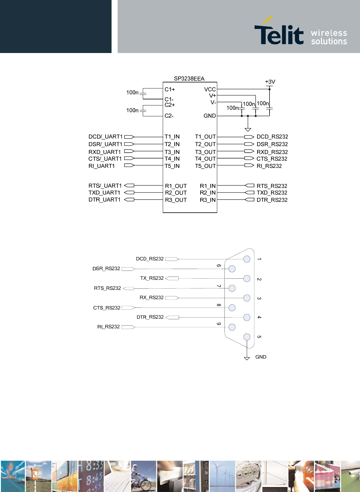
3.6.1. RS232C Interface and Level Translation
In order to interface the module with a PC com port or a RS232 (EIA/TIA-232)
application, a level translator is required.
The RS232 UART 16450, 16550, 16650 and 16750 chipsets accept signals with
lower levels on the RS232 side (EIA/TIA-562), allowing for a lower voltage-
multiplying ratio on the level translator.
Note that the negative signal voltage must be less than 0 V so that some form of
level translation is always required.
The simplest way to translate the levels and invert the signal is by using a single chip
level translator.
There are several of them, differing in the number of driver and receiver and in the
levels.
NOTE: Always make sure you use a true RS232 level translator and not a translator
for RS485 or any other standard.
By convention, the driver is the level translator from the 0-3V UART level to the
RS232 level, while the receiver is the translator from RS232 level to 0-3V UART.
In order to translate the whole set of control lines of the UART you need five drivers
and three receivers.
The figure below shows an example of level translation circuitry:
CC864-DUAL Hardware User Guide
80pppSTzzzzza Rev. 0.4 - dd/mm/yy
Reproduction forbidden without Telit Communications S.p.A’s. written authorization - All Rights Reserved. Page 28 of 49
The RS232 serial port lines are usually connected to a DB9 connector with the layout
shown in the following figure:
3.6.2. 5V UART Level Translation
If the host application uses a microcontroller with a serial port (UART) that works at a
voltage different from 2.8~3V, a circuitry must be provided to adapt the different
levels of the two signal sets.
As for the RS232 translation, there is a selection of single chip translators, but since
the translation requires very few components, a discrete design can also be used.
The following example shows a possible inexpensive translator circuit for a 5V
transmitter/receiver:
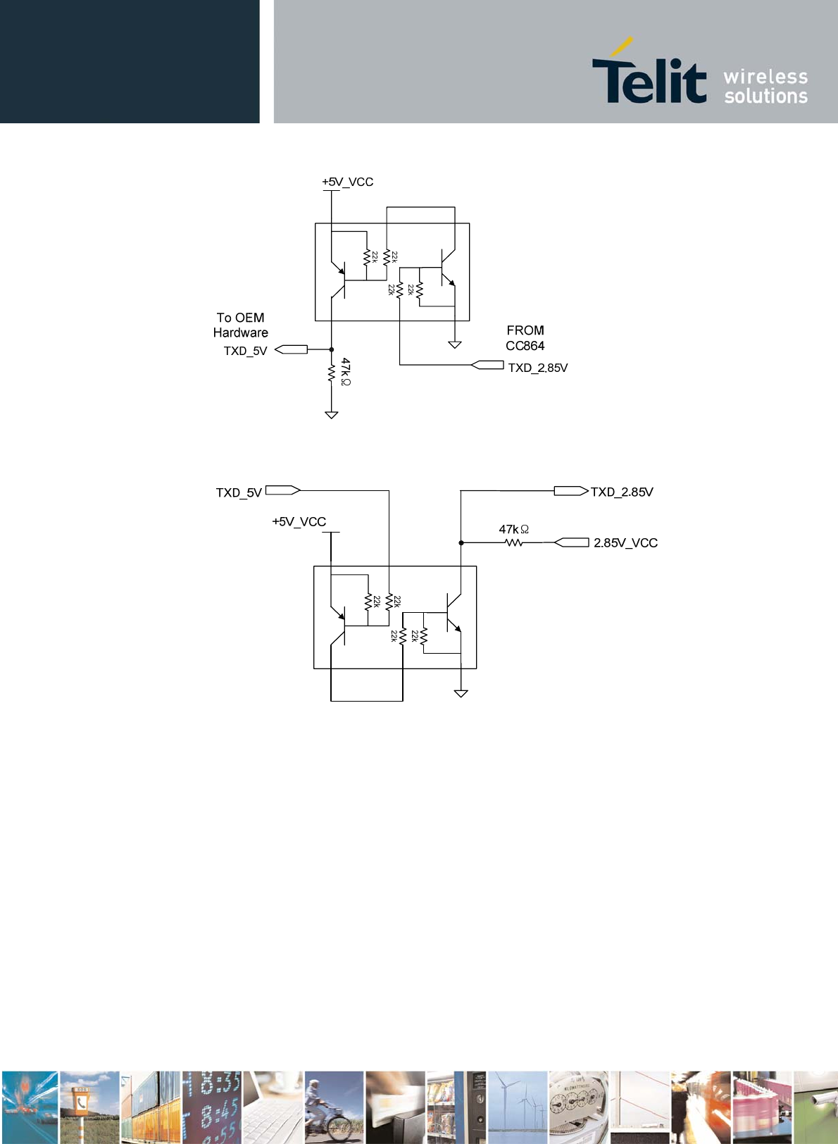
CC864-DUAL Hardware User Guide
80pppSTzzzzza Rev. 0.4 - dd/mm/yy
Reproduction forbidden without Telit Communications S.p.A’s. written authorization - All Rights Reserved. Page 29 of 49
The following example shows a possible inexpensive translator circuit for a 5V
receiver:
3.7. External R-UIM Interface
The Removable User Identify Module (R-UIM) is a smart card for CDMA cellular
applications, with the following features:
• It provides personal authentication information that allows the mobile station
or handset to be connected with the network
• It enables handset independence for the user
• It can be inserted into any CDMA R-UIM equipped handset, allowing the user
to receive or make calls, and also to receive other subscribed services from
any R-UIM equipped handset
The internal power management circuits, R-UIM circuits, and R-UIM pins allow for
2.85V cards via a direct connection.
3.7.1. R-UIM Design Guidelines
The table below contains the pin description of R-UIM holders.
CC864-DUAL Hardware User Guide
80pppSTzzzzza Rev. 0.4 - dd/mm/yy
Reproduction forbidden without Telit Communications S.p.A’s. written authorization - All Rights Reserved. Page 30 of 49
Pin No Signal Name Signal Description Direction
18 VREG_RUIM Power supply CC864-Dual R-UIM
19 UIM_RST Reset signal CC864-Dual R-UIM
20 UIM_DATA Serial data CC864-Dual R-UIM
21 UIM_IN(PWR_DIS) Power disable CC864-Dual R-UIM
22 UIM_CLK Clock CC864-Dual R-UIM
3.8. USB Interface
The CC864-Dual module includes a universal serial bus (USB) transceiver, which
operates at USB low-speed (1.5Mbits/sec) and USB full-speed (12Mbits/sec).
It is compliant with the USB 2.0 specification and can be used for diagnostic
monitoring, control and data transfers.
The table below describes the USB interface signals:
Pin No Signal Usage
35 USB_ID Analog input to detect the USB peripheral type. Left floating,
grounded, or resistor to ground by the peripheral
48 USB_VBUS
Power supply for the internal USB transceiver. This pin is
configured as an analog input or/and output depending on
the type of peripheral device connected
79 USB_D+ Plus(+) line of the differential, bi-directional USB signal
to/from the peripheral device
80 USB_D- Minus(+) line of the differential, bi-directional USB signal
to/from the peripheral device
3.9. Audio Interface
The CC864-DUAL contains two different bi-directional audio blocks:
• MT lines can be used for handset function
• HF lines can be used for hands-free function or earphone function
Only one of the blocks can be active at a time, selected by the AXE input pin or by an
AT-command.
There are three types of audio interface configurations:
• Handset configurations (low power, typically a handset)
• Hands-free configurations (low power, typically an earphone)
• Car kit speakerphone configurations (high power, typically a speaker)
CC864-DUAL Hardware User Guide
80pppSTzzzzza Rev. 0.4 - dd/mm/yy
Reproduction forbidden without Telit Communications S.p.A’s. written authorization - All Rights Reserved. Page 31 of 49
3.9.1. General Design Rules
There are several possible configurations for the audio paths, but the two main types
are balanced and unbalanced microphone configurations.
You are recommended to keep the whole microphone path balanced even if this
means having two wires connecting the microphone instead of one needed in the
unbalanced case.
NOTE: The balanced circuitry is preferred because of its good common mode noise
rejection.
TIP: Keep the analog microphone traces on the PCB and any wires as short as
possible and make sure that the microphone traces on the PCB do not cross or run
parallel to noisy traces (especially power traces).
TIP: If your application requires an unbalanced microphone, keep the traces on the
PCB balanced and unbalance the path as close as possible to the microphone or
wire connector.
TIP: Put a ground trace connected to the ground plane by several vias all around the
microphone lines in order to simulate a shielded trace on the PCB.
The module provides two audio paths in the receive section; only one of the paths
can be active at a time, selectable by the AXE input signal or with an A- command.
The table below lists the audio connections that can be used for the CC864-Dual
module.
Pin number Pin name Pin type Functional description
16 MIC_MT- AI Microphone #1 input (-)
15 MIC_MT+ AI Microphone #1 input (+)
14 MIC_HF- AI Microphone #2 input (-)
13 MIC_HF+ AI Microphone #2 input (+)
10 EAR_HF- AO Headphone output #1 (right side)
9 EAR_HF+ AO Headphone output #2 (left side)
12 EAR_MT+ AO Earphone amplifier output (+)
11 EAR_MT- AO Earphone amplifier output (-)
3.9.2. Handset Interface
The earpiece output pins are connected directly to the handset earpiece, each with
its own bypass capacitor.
The capacitor value is selected to optimize performance in each design, but a value
of 100pF or less is suggested.
The output power for the differential EAR1 output is typically 50mW for a full-scale
+3dBm sine wave into a 32 Ohm speaker.
Each microphone pin requires a 2.2K bias resistor. The positive microphone terminal
is connected to the Bias power (1.8V) through one of the 2.2K resistors. The 1.8V
output provides up to 1mA bias current for the microphone. In addition, each

CC864-DUAL Hardware User Guide
80pppSTzzzzza Rev. 0.4 - dd/mm/yy
Reproduction forbidden without Telit Communications S.p.A’s. written authorization - All Rights Reserved. Page 32 of 49
connection includes a bypass capacitor (27pF is used in the example below), and a
100pF capacitor is connected across the differential pair near the earpiece.
The following figure shows a typical “handset”-interface.
MIC_MT-
1.8V
1uF
Earpiece
32
100pF
100pF
100pF
MIC1
27pF
27pF
2.2KΩ
2.2KΩ
MIC_MT+
EAR_MT-
EAR_MT+
CC864-Dual
Module
Pin 15
Pin 16
Pin 12
Pin 11
3.9.3. Headset Interface
This configuration uses a standard mono single-ended microphone interface.
The positive input contains the signal and is AC-coupled directly to the microphone,
while the negative input is AC-coupled to ground. A 100pF capacitor is connected
across the two AC-coupling capacitors on the microphone side.
A 27pF capacitor bypasses the microphone output.
The positive microphone terminal is connected to the bias voltage (1.8V) through a
2.2 Ohm bias resistor. The 1.8V output provides up to 1 mA bias current for the
microphone.
The bias power is bypassed by a 0.1uF capacitor.
The figure below shows the basic “headset”-configuration.
CC864-DUAL Hardware User Guide
80pppSTzzzzza Rev. 0.4 - dd/mm/yy
Reproduction forbidden without Telit Communications S.p.A’s. written authorization - All Rights Reserved. Page 33 of 49
MIC_HF-
1.8V
1uF
HS earpiece
16
33uF
100pF
HS
MIC
27pF
2.2KΩ
MIC_HF+
EAR_HF-
EAR_HF+
CC864-Dual
Module
Pin 13
Pin 14
Pin 9
Pin 10
+
-
The module also supports a differential “headset” interface as shown in the figure
below.
MIC_HF-
1.8V
HS earpiece
32
100pF
HS
MIC
27pF
2.2KΩ
MIC_HF+
EAR_HF-
EAR_HF+
CC864-Dual
Module
Pin 13
Pin 14
Pin 9
Pin 10
27pF
27pF
3.9.4. Car Kit Speakerphone Interface
For the “car kit speaker phone”configuration, the power output requirement is usually
at least 4W; therefore an amplifier is required to boost the CC864-Dual audio output.
CC864-DUAL Hardware User Guide
80pppSTzzzzza Rev. 0.4 - dd/mm/yy
Reproduction forbidden without Telit Communications S.p.A’s. written authorization - All Rights Reserved. Page 34 of 49
The design of the amplifier should comply with the following guidelines:
• The input to the amplifier must be taken from the “EAR_HF” audio path of the
module.
• The amplifier must have a mute control to be used while not in conversation
to eliminate the background noise, and to save power.
• The power to the amplifier must be decoupled as much as possible from the
CC864-Dual module power supply, by either keeping separate wires or by
placing bypass capacitors of adequate value close to the amplifier power
input Pins.
• The biasing voltage of the amplifier must be stabilized with low ESR (for
example, a tantalum) capacitor of adequate value.
The figure below shows an example of car kit amplifier schematic.
3.10. PCM Interface
The CC864-Dual module can support PCM interface. It can runs at 128kHz ~
2.048Mhz. The PCM interface enables communication with an external CODEC to
support hands-free application. Linear, -law, and A-law CODECs are supported by
the PCM interface.
PCM interface can be configured and controlled by either direct register access
through the CODEC_CTL register, or by the aDSP CODEC configuration command.
To change CODEC_CTL register, use AT-command.

CC864-DUAL Hardware User Guide
80pppSTzzzzza Rev. 0.4 - dd/mm/yy
Reproduction forbidden without Telit Communications S.p.A’s. written authorization - All Rights Reserved. Page 35 of 49
AT-command is
AT#DVI=<mode>[,<dviport>,<clockmode>].
Pin
Number Name I/O Description Level
36 PCM_CLOCK I/O PCM_CLOCK CMOS 2.8V
63 TGPIO_10/PCM_TX I/O TGPIO10 Configurable
GPIO/PCM_TX
CMOS 2.8V
65 TGPIO_18/PCM_RX I/O TGPIO18 Configurable
GPIO/PCM_RX
CMOS 2.8V
71 TGPIO_17/PCM_SYN
C
I/O TGPIO17 Configurable
GPIO/PCM_SYNC
CMOS 2.8V
3.11. I2C Bus Interface
The I2C is a two-wire bus for Inter-IC communication widely supported by peripheral
components.
Two wires (or lines); serial data (SDA) and serial clock (SCL) carry information
between the connected devices.
Each device is recognized by a unique address (whether it’s a microcontroller,
memory, LCD driver, stereo DAC, or keyboard interface) and can operate as either a
transmitter or receiver, depending on the device function.
Pin No Name Description
33 SCL Serial BUS Clock
34 SDA Serial BUS Data
3.12. ADC/DAC Interface
The CC864-Dual module provides three ADC converters and one DAC converter.
Pin No Name Description
37 ADC_IN1 Analog/Digital converter input
38 ADC_IN2 Analog/Digital converter input
39 ADC_IN3 Analog/Digital converter input
40 DAC_OUT Digital/Analog converter output
3.12.1. ADC Converter
3.12.1.1. Description
The CC864-Dual module provides three on-board ADC converters.
CC864-DUAL Hardware User Guide
80pppSTzzzzza Rev. 0.4 - dd/mm/yy
Reproduction forbidden without Telit Communications S.p.A’s. written authorization - All Rights Reserved. Page 36 of 49
Parameter Min Max
Input Voltage Range 0V 2.5 V
Resolution 10 bit
Accuracy 8 bit
Clock rate 2.4Mhz
Analog measurement output or sensor output (battery voltage, temperature etc) can
be connected to the ADC pin with proper signal conditioning and be read by an AT-
command.
3.12.1.2. Using ADC Converter
An AT-command is available to use the ADC function
The command is
AT#ADC=1,2
The read value is expressed in mV
Refer to SW User Guide or AT Commands Reference Guide for the full description of
this function.
3.12.2. DAC Converter
3.12.2.1. Description
The CC864-Dual module provides a digital to analog converter (DAC).
Parameter Min Max
Input Voltage Range 0V 2.8 V
Resolution 8 bit
Clock rate 4.8Mhz
The precision is 8 bits so, if we consider that the maximum voltage is 2V, the
integrated voltage could be calculated with the following formula:
Integrated output voltage = (2 × value)/255
3.12.2.2. Enabling the DAC
An AT-command is available to use the DAC function
The command is
AT#DAC[=<enable>[,<value>]]
<value> - scale factor of the integrated output voltage(0…255 -8 bit precision) and
must be present if <enable>=1
Refer to the SW User Guide or AT commands Reference Guide for the full
description of this function.
CC864-DUAL Hardware User Guide
80pppSTzzzzza Rev. 0.4 - dd/mm/yy
Reproduction forbidden without Telit Communications S.p.A’s. written authorization - All Rights Reserved. Page 37 of 49
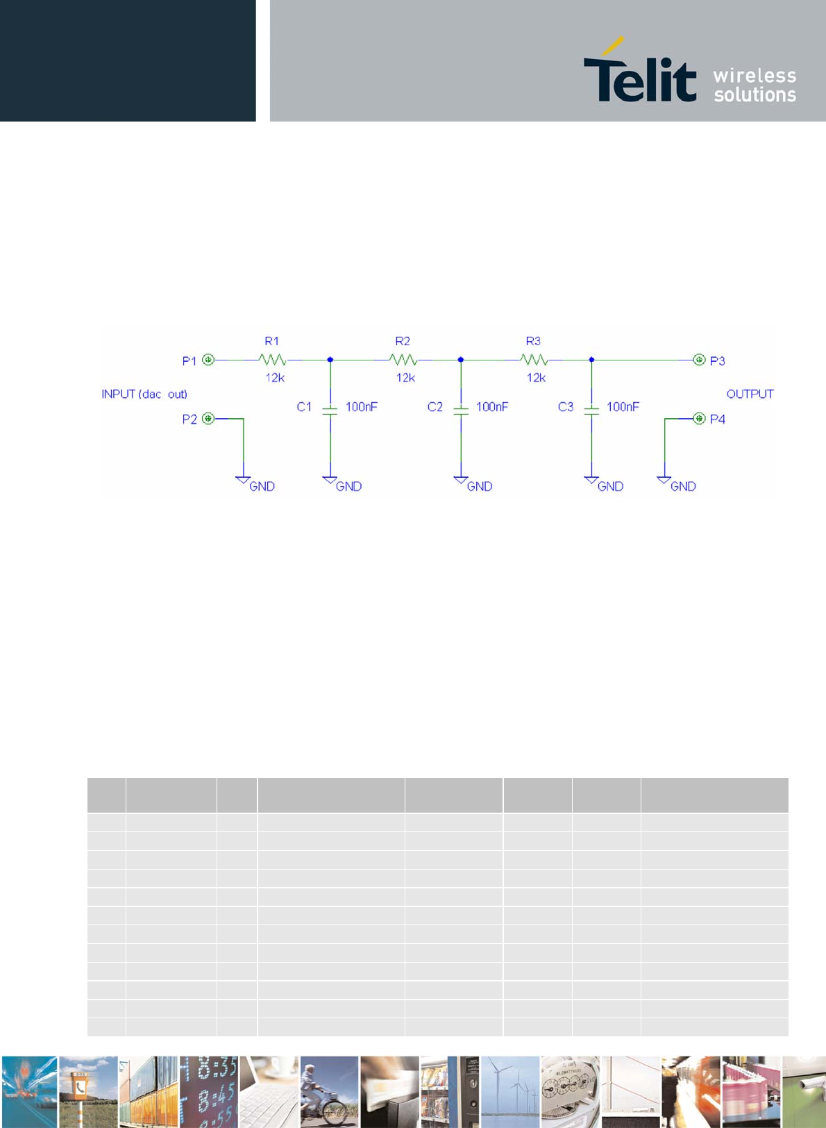
3.12.2.3. Low Pass Filter Example
The DAC pin drives out the PDM (Pulse Density Modulation) signal. It is a square
wave output.
The application needs an additional RC filter to convert the PDM output to an analog
signal.
The figure below shows an example of Low Pass filter. Final tuning is needed to find
the exact values of resistors and capacitors for the target application.
3.13. General Purpose I/O
The general purpose I/O Pins can be configured to act in three different ways:
• Input: Input Pins can only be read. They report the digital value (high or low)
present on the Pin at the read time.
• Output: output Pins can be written or queried. They can be used to set the
value of the Pin output.
• Alternate function (internally controlled): An alternate function pin is
internally controlled by the CC864-Dual firmware and acts depending on the
currently selected function.
Pin Signal I/O Function Type Default
state On_OF
F state Alternative
Function
70 TGPIO_01 I/O Configurable GPIO CMOS 2.8V Input Low
74 TGPIO_02 I/O Configurable GPIO CMOS 2.8V Input Low
66 TGPIO_03 I/O Configurable GPIO CMOS 2.8V Input Low AUDIO MUTE
59 TGPIO_04 I/O Configurable GPIO CMOS 2.8V Input Low CONVERSATION
78 TGPIO_05 I/O Configurable GPIO CMOS 2.8V Input Low RFTXMON
68 TGPIO_06 I/O Configurable GPIO CMOS 2.8V Input ALARM
73 TGPIO_07 I/O Configurable GPIO CMOS 2.8V Input Low BUZZER
67 TGPIO_08 I/O Configurable GPIO CMOS 2.8V Input Low POWER_SAVING
76 TGPIO_09 I/O Configurable GPIO CMOS 2.8V Input Low
63 TGPIO_10 I/O Configurable GPIO CMOS 2.8V Input Low PCM_TX
57 TGPIO_11 I/O Configurable GPIO CMOS 2.8V Input Low VIBRATOR
62 TGPIO_12 I/O Configurable GPIO CMOS 2.8V Input Low CALL_KEY
CC864-DUAL Hardware User Guide
80pppSTzzzzza Rev. 0.4 - dd/mm/yy
Reproduction forbidden without Telit Communications S.p.A’s. written authorization - All Rights Reserved. Page 38 of 49
77 TGPIO_13 I/O Configurable GPIO CMOS 2.8V Input Low ACTIVE
60 TGPIO_14 I/O Configurable GPIO CMOS 2.8V Input Low
61 TGPIO_15 I/O Configurable GPIO CMOS 2.8V Input Low
75 TGPIO_16 I/O Configurable GPIO CMOS 2.8V Input Low
71 TGPIO_17 I/O Configurable GPIO CMOS 2.8V Input Low PCM_SYNC
65 TGPIO_18 I/O Configurable GPIO CMOS 2.8V Input Low PCM_RX
56 TGPIO_19 I/O Configurable GPIO CMOS 2.8V Input Low
58 TGPIO_20 I/O Configurable GPIO CMOS 2.8V Input Low
72 TGPIO_21 I/O Configurable GPIO CMOS 2.8V Input High
64 TGPIO_22 I/O Configurable GPIO CMOS 1.8V Input Low
Warning: TGPIO_22 has 1.8V CMOS level tolerance. This is to be compatible with
the Telit Unified Form Factor.
3.13.1. Using a GPIO pin as Input
The GPIO pins, when used as input, can be connected to a digital output of another
device to report its status, provided this device has interface levels compatible with
the 2.8V CMOS levels of the GPIO.
3.13.2. Using a GPIO pin as Output
The GPIO pins, when used as outputs, can drive 2.8V CMOS digital devices or
compatible hardware.
When set as outputs, the pins have a push-pull output and therefore the pull-up
resistor can be omitted.
3.13.3. TGPIO_03/AUDIO MUTE
This pin can be used to mute audio e.g. when an external audio amplifier is used for
the car kit speaker function.
It is always desirable to have a mute control on the amplifier, in order to turn it off
while the device is not sending signal to the output, so that the amplifier background
noise which may be audible during idle condition is cut off.
3.13.4. TGPIO_04/RF Transmission Control
When configured as RF transmission controlinput, this pin permits disabling the
transmitter when the GPIO is set to low by the application.
3.13.5. TGPIO_05/RFTXMON
When configured as RFTMON output, this pin is controlled by the CC864-Dual only.
It is High when the transmitter is active, and Low when the transmitter activity is
completed.

CC864-DUAL Hardware User Guide
80pppSTzzzzza Rev. 0.4 - dd/mm/yy
Reproduction forbidden without Telit Communications S.p.A’s. written authorization - All Rights Reserved. Page 39 of 49
For example, if a call is started, the line is high during all of the conversation (RF
Transmit) and low after the call is hung up.
3.13.6. TGPIO_06/ALARM
This pin, when configured as alarm output, is controlled by the CC864-Dual.
It goes high when the alarm starts, and low again after the issue of a dedicated AT-
command.
You can use this output to power up the module itself or the external application at
the alarm time, giving you the possibility to program a timely system wake-up to
perform periodic actions while completely turning off either the application or the
module during sleep periods, considerably reducing power consumption.
Refer to SW User Guide or AT commands Reference Guide for the full description of
this function.
3.13.7. TGPIO_07/BUZZER
This pin, when configured as buzzer output, is controlled by the module.
It drives a buzzer driver with appropriate square waves, and permits your application
to easily implement the buzzer feature with ringing tones, melody played at the call
incoming, tone playing on SMS incoming, or simply playing a tone or melody when
needed by your application.
The following figure shows an example of the TGPIO_07/BUZZER configuration:
CC864-DUAL Hardware User Guide
80pppSTzzzzza Rev. 0.4 - dd/mm/yy
Reproduction forbidden without Telit Communications S.p.A’s. written authorization - All Rights Reserved. Page 40 of 49
3.13.8. TGPIO_08/POWER_SAVING
When configured as power saving, the host gives this signal to the module, setting
the module into power saving mode.
This signal is active low.
When the module enters power saving mode, every active items, including the UART
port is turned off, so that current consumption is considerably reduced.
3.13.9. TGPIO_11/VIBRATOR
When configured as vibrator output, this pin is controlled by the module and it starts
with appropriate square waves.
For a reference, see the Buzzer circuitry in section 3.13.7.
3.13.10. TGPIO_12/CALL_KEY
When configured as call key, this pin is used to connect outgoing call or to respond to
incoming call.
If automatic answer is disabled, the equivalent AT command is “ATA”.
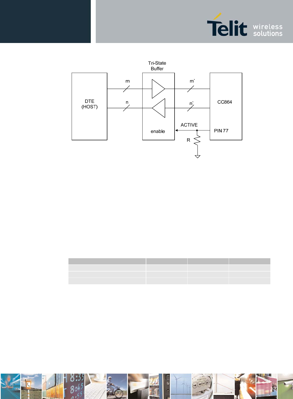
3.13.11. TGPIO_13/ACTIVE
When configured as active, this signal is used as a control signal to enable the buffer
between the module and the host.
When the reset procedure and boot sequence is successful, the module drives the
signal active high, and its output is low when the module is powered off.
Therefore, an external pull-down resistor is needed to define the state at power off if
this feature is used.
Note: Using buffers for most signals (except ON/OFF, RESET, STAT_LED) between
the module and the host to prevent leakage currents from the host (while powered
on) to the module (while powered off) is recommended. Leakage current can cause a
reset failure in the module.
CC864-DUAL Hardware User Guide
80pppSTzzzzza Rev. 0.4 - dd/mm/yy
Reproduction forbidden without Telit Communications S.p.A’s. written authorization - All Rights Reserved. Page 41 of 49
3.14. Miscellaneous Interface Signals
3.14.1. VAUX1
A regulated power supply output is provided in order to supply small devices from the
module itself.
This output is active when the module is on, and shuts off when the module is shut
down.
The operating range characteristics of the supply are listed in the table below:
Operating Range –VAUX1 Power supply
Parameters Min Typical Max
Output voltage 2.75V 2.85V 2.90V
Output current 150mA
Output bypass capacitor 1uF
3.14.2. VRTC
The VRTC pin brings out the real time clock supply, which is separated from the rest
of the module’s internal power supply, allowing the RTC to operate when all the other
parts of the devices are turned off.
A backup capacitor can be added to this pin.
The backup capacitor is charged when the module is on, and it supplies power to the
RTC circuit when the module is turned off.
CC864-DUAL Hardware User Guide
80pppSTzzzzza Rev. 0.4 - dd/mm/yy
Reproduction forbidden without Telit Communications S.p.A’s. written authorization - All Rights Reserved. Page 42 of 49
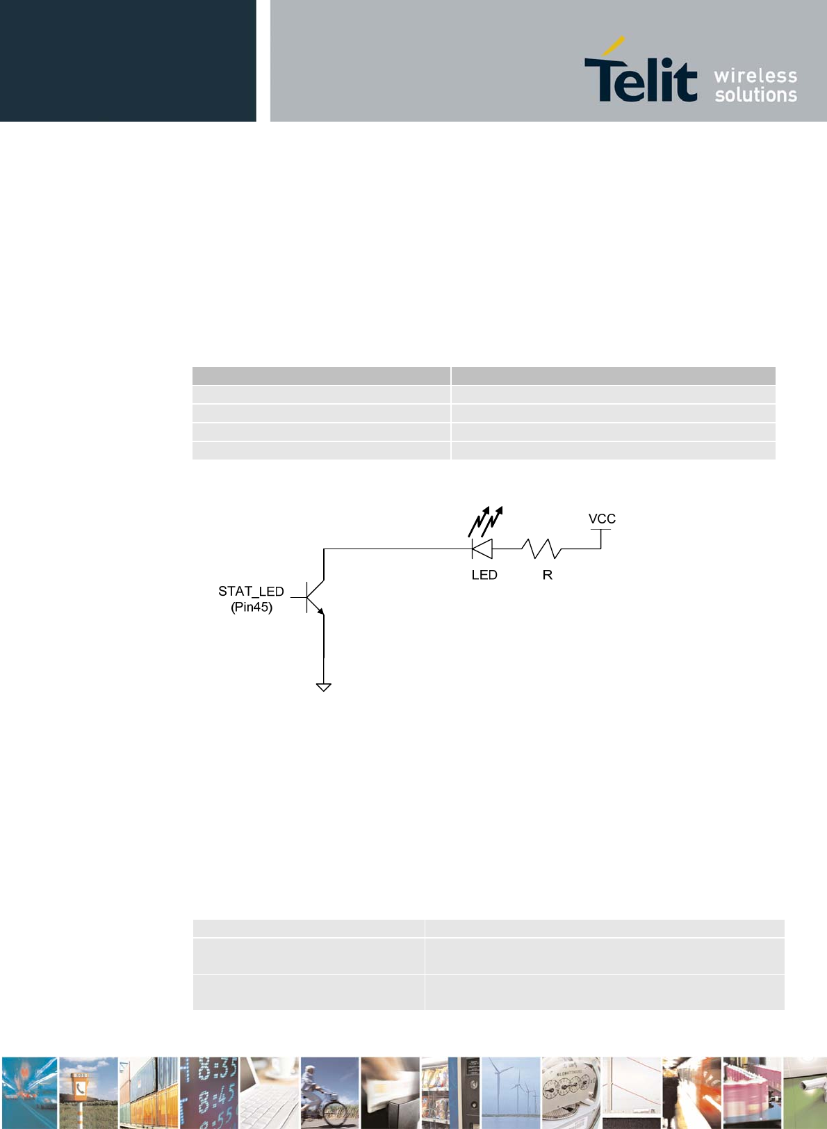
3.14.3. STAT_LED
This pin is an open collector output signal.
The STAT_LED pin status shows information on the network service availability and
Call status.
In the CC864-Dual module, the STAT_LED usually needs an external transistor to
drive an external LED.
Therefore, the status indicated in the following table is reversed with respect to the
pin status.
LED status Device Status
Permanently off Device off
Fast blinking(Period 1s, Ton 0.5s) Net search/Not registered/Turning off
Slow blinking(Period 3s, Ton 0.3s) Registered full service
Permanently on A call is active
3.14.4. PWRMON
This pin is internally connected to a power source of the internal interface voltage
corresponding to the 2.8V CMOS high level.
If the reset procedure or boot sequence is finished successfully, PWRMON is
changed to high state.
3.14.5. AXE
This pin can be used for audio path switching.
You can select the handset path or hand free path with this signal.
State Audio Path
Low Handset mode
(Tx: MIC_MT+/-, Rx:EAR_MT+/-)
High Hands free mode
(Tx:MIC_HF+/-, Rx:EAR_HF+/- or EAR_HF+)

CC864-DUAL Hardware User Guide
80pppSTzzzzza Rev. 0.4 - dd/mm/yy
Reproduction forbidden without Telit Communications S.p.A’s. written authorization - All Rights Reserved. Page 43 of 49
If this pin is set to a low state, the module uses the handset audio path. And if set to
a high state, the module changes the audio path to hands free mode from handset
mode.
CC864-DUAL Hardware User Guide
80pppSTzzzzza Rev. 0.4 - dd/mm/yy
Reproduction forbidden without Telit Communications S.p.A’s. written authorization - All Rights Reserved. Page 44 of 49
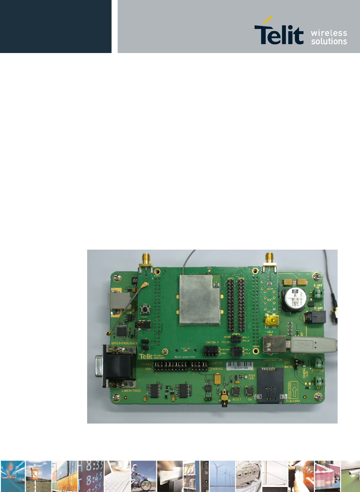
4. Development and Testing
In order to assist you with the development of your Telit CC864-Dual module based
application, Telit can supply the EVK2 Evaluation kit with appropriate power supply,
R-UIM card housing, RS232 serial port level translator, direct UART connection, USB
connection, Handset, Headset and Hands-free(car kit) audio and antenna.
The EVK2 provides a fully functional reference solution for a data/phone application.
The standard serial RS232 9-pin interface connector and USB interface provided on
the evaluation kit allow the connection of the EVK2 system to a PC or other DTE.
The development of the application utilizing the Telit CC864-Dual module must use
proper designs of all the interfaces to and from the module (for example, power
supply, audio paths, level translators), otherwise a decrease in the performance will
be introduced or, in the worst case, a faulty design can even lead to an operational
failure of the module.
In order to assist the hardware designer, the EVK2 board presents a series of
different solutions, which cover the most common design requirements on the market,
and which can be easily integrated in the OEM design as building blocks or can be
taken or can be taken as starting points to develop a specific solution.
CC864-DUAL Hardware User Guide
80pppSTzzzzza Rev. 0.4 - dd/mm/yy
Reproduction forbidden without Telit Communications S.p.A’s. written authorization - All Rights Reserved. Page 45 of 49
5. Acronyms and Abbreviations
Term Definition
ADC Analog-to-Digital Converter
CDMA Code Division Multiple Access
DAC Digital-to-Analog Converter
EVRC Enhanced Variable Rate CODEC
GPIO General Purpose Input / Output
GPS Global Positioning System
HF Hands-free
I2C Inter-Integrated Circuit
JDR Jammer Detector
JTAG Joint Test Action Group(ANSI/ICEEE Std. 1149.1-1990)
MT Micro Telephone or HandSet (MT or HS)
PCM Pulse Coded Modulation
PDM Pulse Density Modulation (in a DAC)
RTC Real Time Clock
R-UIM Removable User Identity Module
S-GPS Simultaneous-GPS
TGPIO Telit General Purpose Input / Output
UART Universal Asynchronous Receiver Transmitter
USB Universal Serial Bus
VAUX Voltage Auxiliary
ZIF Zero Intermediate Frequency
CC864-DUAL Hardware User Guide
80pppSTzzzzza Rev. 0.4 - dd/mm/yy
Reproduction forbidden without Telit Communications S.p.A’s. written authorization - All Rights Reserved. Page 46 of 49
6. Appendix: Pin Allocation
The table below lists the complete pin allocation on the system connector of the
CC864-DUAL.
Pin Signal I/O Function Internal
Pull up Type
Power Supply
1 VBATT - Main power supply Power
2 VBATT - Main power supply Power
3 VBATT - Main power supply Power
4 VBATT - Main power supply Power
5 GND - Ground Power
6 GND - Ground Power
7 GND - Ground Power
Audio
8 AXE I Hands free switching 100K CMOS
2.8V
9 EAR_HF+ AO Hands free ear output, phase+ Audio
10 EAR_HF- AO Hands free ear output, phase- Audio
11 EAR_MT+ AO Handset earphone signal output, phase+ Audio
12 EAR_MT- AO Handset earphone signal output, phase- Audio
13 MIC_HF+ AI Hands free microphone input ; phase+,
nominal level 3mVrms
Audio
14 MIC_HF- AI Hands free microphone input ; phase-,
nominal level 3mVrms
Audio
15 MIC_MT+ AI Handset microphone signal input ;
phase+, nominal level 50mVrms
Audio
16 MIC_MT- AI Handset microphone signal input ; phase-
, nominal level 50mVrms
Audio
R-UIM Card Interface
18 VREG_RUIM - Power supply for the UIM 2.8V
19 UIM_RST O Reset 2.8V
20 UIM_DATA I/O Data I/O 2.8V
21 UIM_IN I Presence(active low) 47K 2.8V
22 UIM_CLK O Clock 2.8V
QCOM Diagnostic Monitor
23 RX_TRACE I RX Data for debug monitor CMOS
2.8V
24 TX_TRACE O TX Data for debug monitor CMOS
2.8V
Program / Data + Hw Flow Control
25 C103/TXD I Serial data input (TXD) from DTE CMOS
2.8V
26 C104/RXD O Serial data output to DTE CMOS
2.8V
27 C107/DSR O Output for Data set ready signal (DSR) to CMOS

CC864-DUAL Hardware User Guide
80pppSTzzzzza Rev. 0.4 - dd/mm/yy
Reproduction forbidden without Telit Communications S.p.A’s. written authorization - All Rights Reserved. Page 47 of 49
DTE 2.8V
28 C106/CTS O Output for Clear to send signal (CTS) to
DTE
CMOS
2.8V
29 C108/DTR I Input for Data terminal ready signal (DTR)
from DTE
CMOS
2.8V
30 C125/RING O Output for Ring indicator signal (RI) to
DTE
CMOS
2.8V
31 C105/RTS I Input for Request to send signal (RTS)
from DTE
CMOS
2.8V
32 C109/DCD O Output for Data carrier detect signal
(DCD) to DTE
CMOS
2.8V
I2C
33 SCL I/O IIC Hardware interface CMOS
2.8V
34 SDA I/O IIC Hardware interface CMOS
2.8V
USB
35 USB_ID I USB_ID input 47K CMOS
2.8V
48 USB_VBUS AI/A
O
USB_VBUS power supply 5V
79 USB_D+ I/O USB Data(USB Internal Transceiver
In/Output)
2.8V~3.6V
80 USB_D- I/O USB Data(USB Internal Transceiver
In/Output)
2.8V~3.6V
DAC and ADC
37 ADC_IN1 AI Analog/Digital converter input A/D
38 ADC_IN2 AI Analog/Digital converter input A/D
39 ADC_IN3 AI Analog/Digital converter input A/D
40 DAC_OUT AO Digital/Analog converter output D/A(PWM)
PCM
36 PCM_CLOCK I/O Telit GPIO Configurable GPIO CMOS
2.8V
63 TGPIO_10/PCM_TX I/O Telit GPIO10 Configurable GPIO CMOS
2.8V
65 TGPIO_18/PCM_RX I/O Telit GPIO18 Configurable GPIO CMOS
2.8V
71 TGPIO_17/PCM_SY
NC
I/O Telit GPIO17 Configurable GPIO CMOS
2.8V
Miscellaneous Functions
45 STAT_LED O Status indicator led CMOS
1.8V
46 GND - Ground Ground
49 PWRMON O Power ON Monitor CMOS
2.8V
50 VAUX1 - Power output for external accessories (AT
command driven)
2.85V/
150mA
51 CHARGE AI Charger input Li-Ion Power
CC864-DUAL Hardware User Guide
80pppSTzzzzza Rev. 0.4 - dd/mm/yy
Reproduction forbidden without Telit Communications S.p.A’s. written authorization - All Rights Reserved. Page 48 of 49
52 CHARGE AI Charger input Li-Ion Power
53 ON/OFF* I Input command for switching power ON
or OFF (toggle command). The pulse to
be sent to the CC864-DUAL must be
equal or greater than 1 second.
47k Pull up to
VBTT
54 RESET* I Reset input
55 VRTC Power
Telit GPIO
56 TGPIO_19 I/O Telit GPIO19 Configurable GPIO CMOS
2.8V
57 TGPIO_11/VIBRATO
R
I/O Telit GPIO11 Configurable GPIO/Vibrator CMOS
2.8V
58 TGPIO_20 I/O Telit GPIO20 Configurable GPIO CMOS
2.8V
59 TGPIO_04/CONVER
SATION
I/O Telit GPIO4 Configurable GPIO/
Conversation
CMOS
2.8V
60 TGPIO_14 I/O Telit GPIO14 Configurable GPIO CMOS
2.8V
61 TGPIO_15 I/O Telit GPIO15 Configurable GPIO CMOS
2.8V
62 TGPIO_12/AUDIO
CALL BUTTON
I/O Telit GPIO12 Configurable GPIO/ Audio
Call Button
CMOS
2.8V
64 TGPIO_22 I/O Telit GPIO22 Configurable GPIO CMOS
1.8V
66 TGPIO_03/AUDIO
MUTE
I/O Telit GPIO03 Configurable GPIO/ Audio
Mute
CMOS
2.8V
67 TGPIO_08/POWER_
SAVING
I/O Telit GPIO08 Configurable GPIO/ Power
saving mode
CMOS
2.8V
68 TGPIO_06/ALARM I/O Telit GPIO06 Configurable GPIO/ Power
wakeup
CMOS
2.8V
70 TGPIO_01 I/O Telit GPIO01 Configurable GPIO CMOS
2.8V
72 TGPIO_21 I/O Telit GPIO21 Configurable GPIO CMOS
2.8V
73 TGPIO_07/BUZZER I/O Telit GPIO07 Configurable GPIO/ Buzzer CMOS
2.8V(PWM
)
74 TGPIO_02 I/O Telit GPIO02 Configurable GPIO CMOS
2.8V
75 TGPIO_16 I/O Telit GPIO16 Configurable GPIO CMOS
2.8V
76 TGPIO_09 I/O Telit GPIO09 Configurable GPIO CMOS
2.8V
77 TGPIO_13/ACTIVE I/O Telit GPIO13 Configurable GPIO/
ACTIVE pin to protect current leakage
CMOS
2.8V
78 TGPIO_05/RFTXMO
N
I/O Telit GPIO05 Configurable GPIO/
Transmitter ON monitor
CMOS
2.8V
Reserved

CC864-DUAL Hardware User Guide
80pppSTzzzzza Rev. 0.4 - dd/mm/yy
Reproduction forbidden without Telit Communications S.p.A’s. written authorization - All Rights Reserved. Page 49 of 49
17
41
42
43
44
47
69
80
Warning: All reserved pins must be left open and unconnected; they may not be
used for any routing purposes on the application PCB (NC/NR pins). They are
reserved for internal Telit use or future expansion.