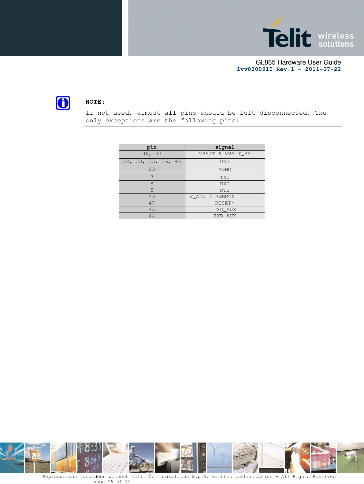
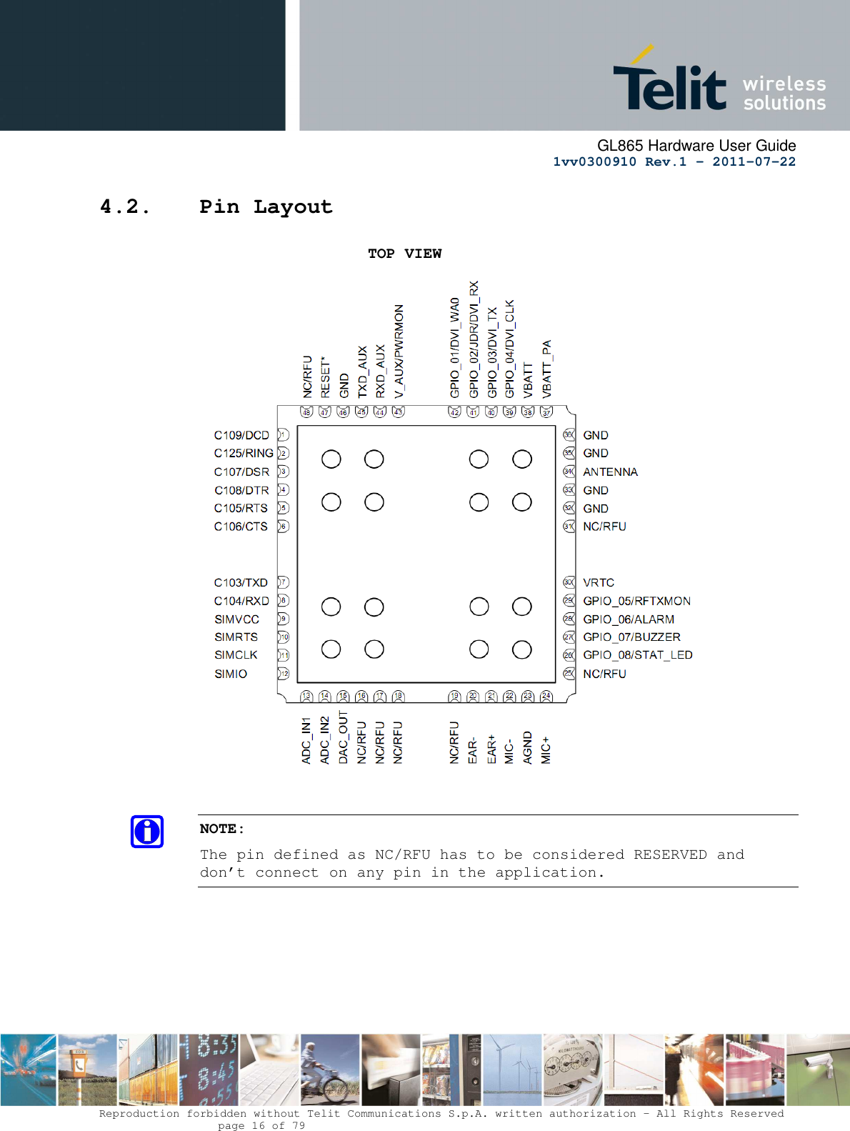
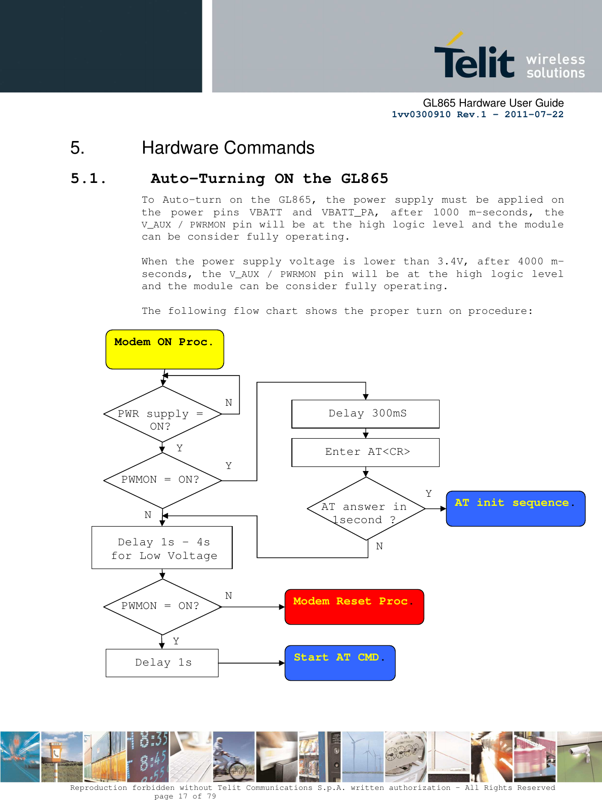
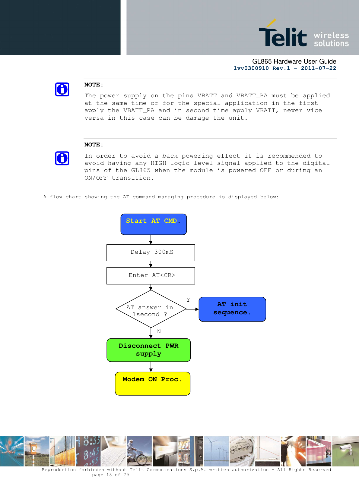
Telit Communications S p A GL865Q Quadband GSM/ GPRS Module User Manual 1vv0300910 GL865 Hardware User Guide r1
Telit Communications S.p.A. Quadband GSM/ GPRS Module 1vv0300910 GL865 Hardware User Guide r1
UserManual.wiki
>
Telit Communications S p A
>
GL865Q User Manual
User Manual
Navigation menu
Upload a User Manual
Namespaces
Wiki Guide
HTML
PDF
Info
Views
User Manual
Discussion / Help
Navigation


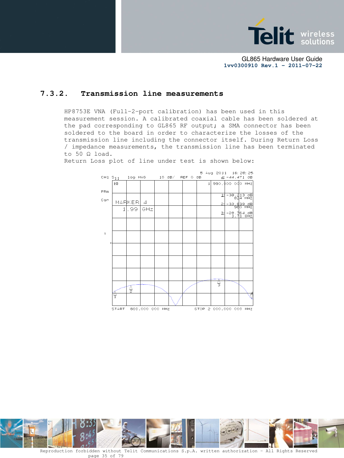
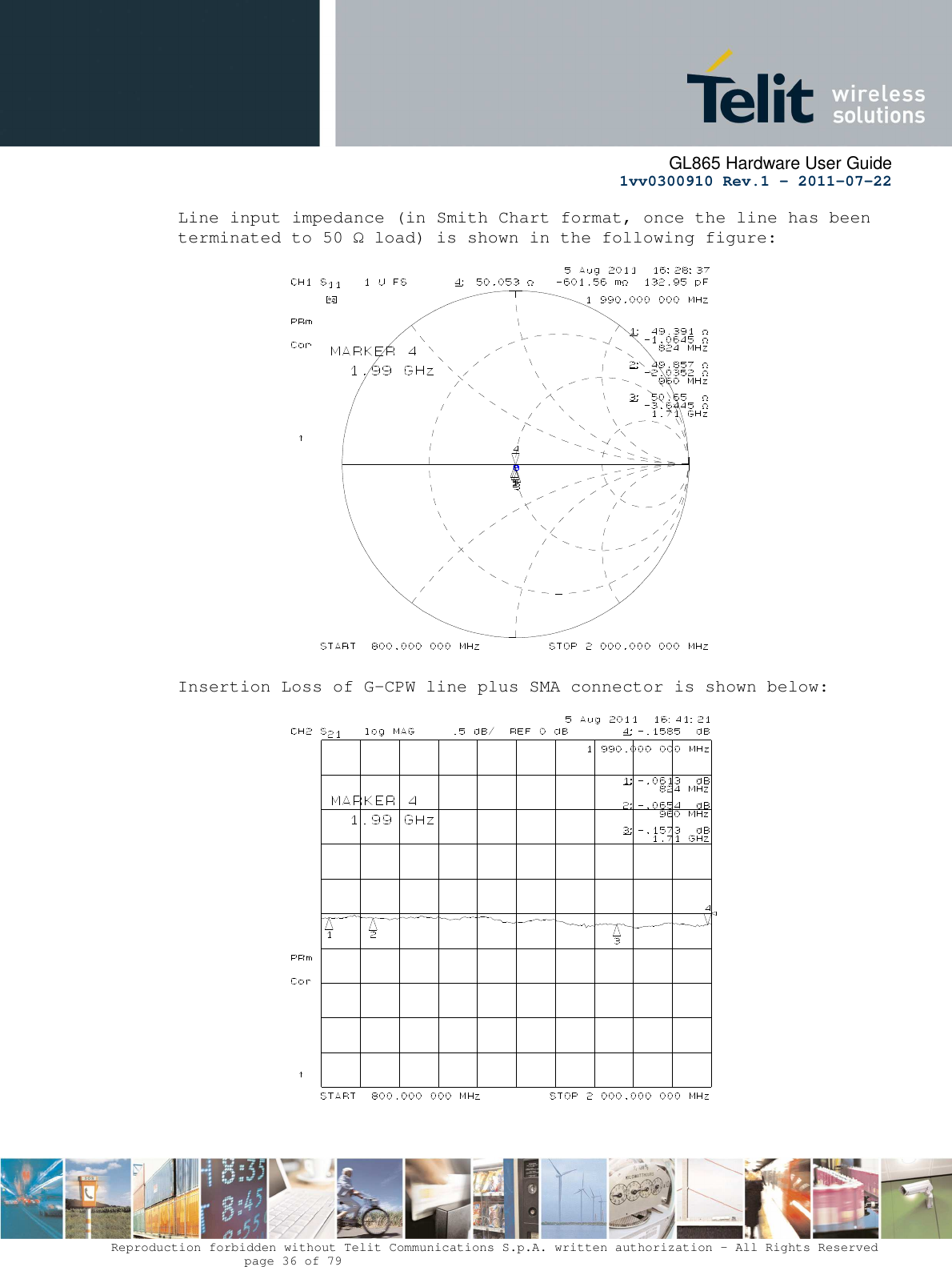


![GL865 Hardware User Guide 1vv0300910 Rev.1 – 2011-07-22 Reproduction forbidden without Telit Communications S.p.A. written authorization - All Rights Reserved page 66 of 79 12.1.2. Enabling DAC An AT command is available to use the DAC function. The command is: AT#DAC= [<enable> [, <value>]] <value> - scale factor of the integrated output voltage (0..1023 - 10 bit precision) it must be present if <enable>=1 Refer to SW User Guide or AT Commands Reference Guide for the full description of this function. NOTE: The DAC frequency is selected internally. D/A converter must not be used during POWERSAVING. 12.1.3. Low Pass Filter Example](https://usermanual.wiki/Telit-Communications-S-p-A/GL865Q/User-Guide-1522322-Page-66.png)