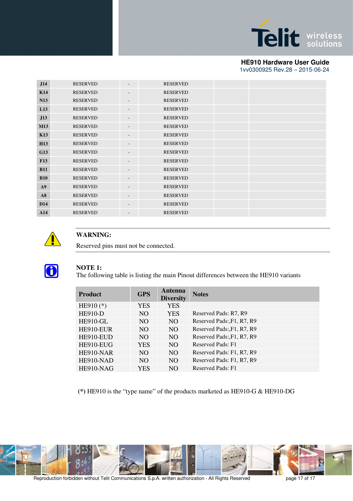
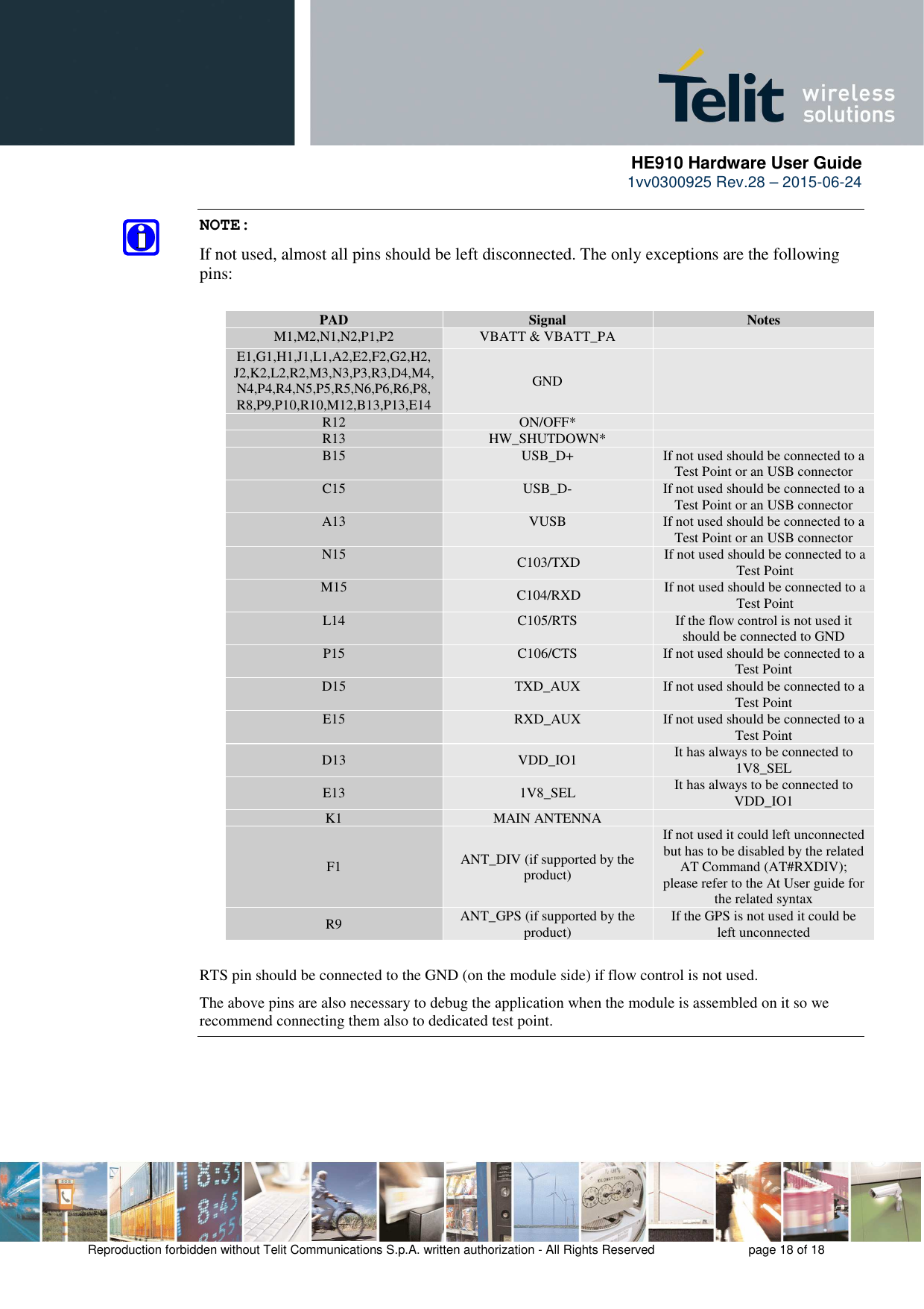
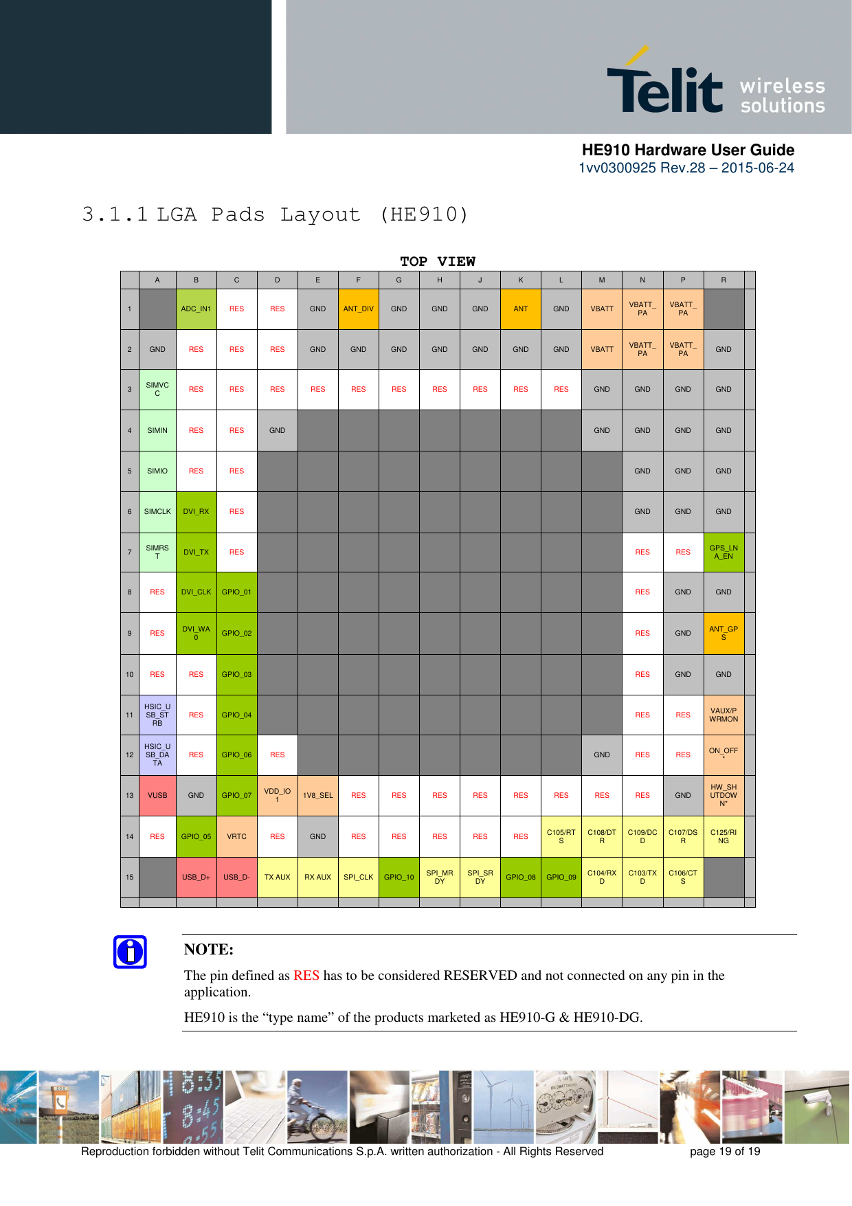
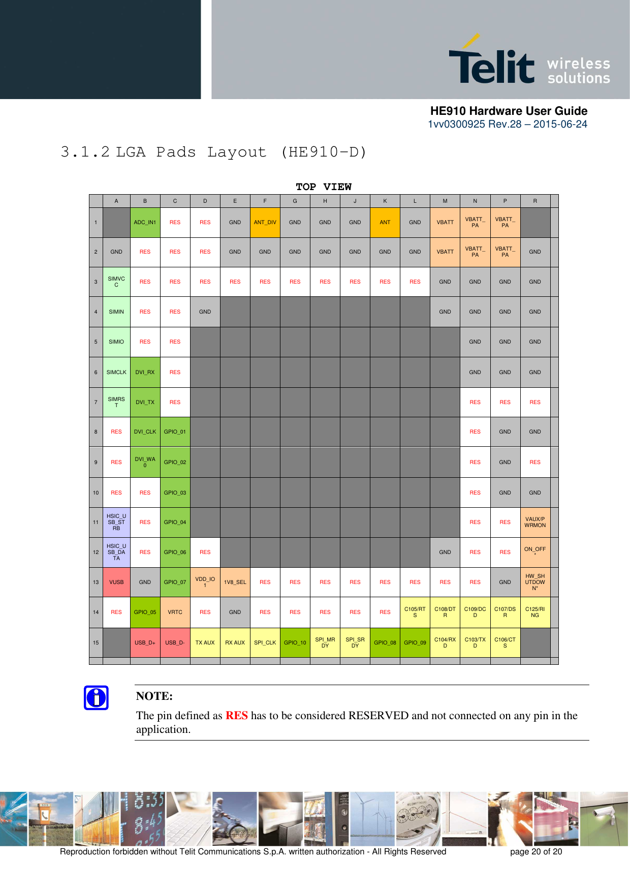
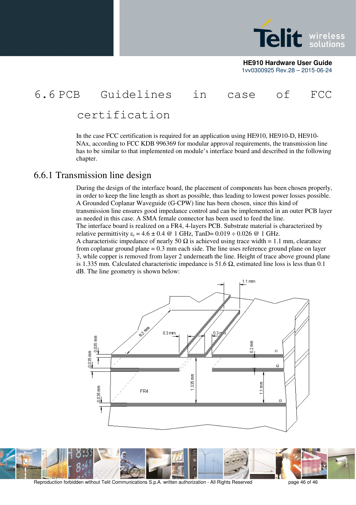
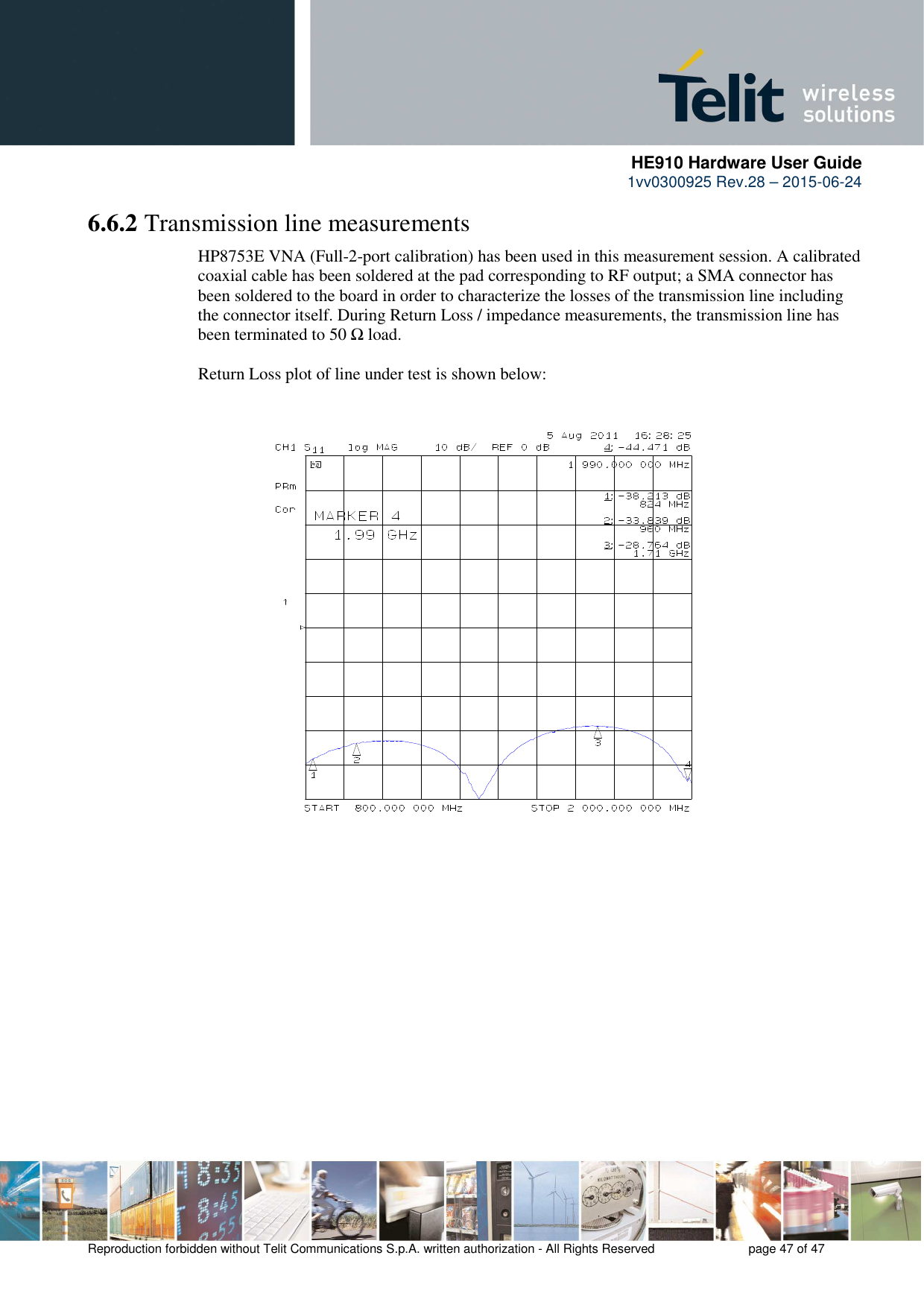
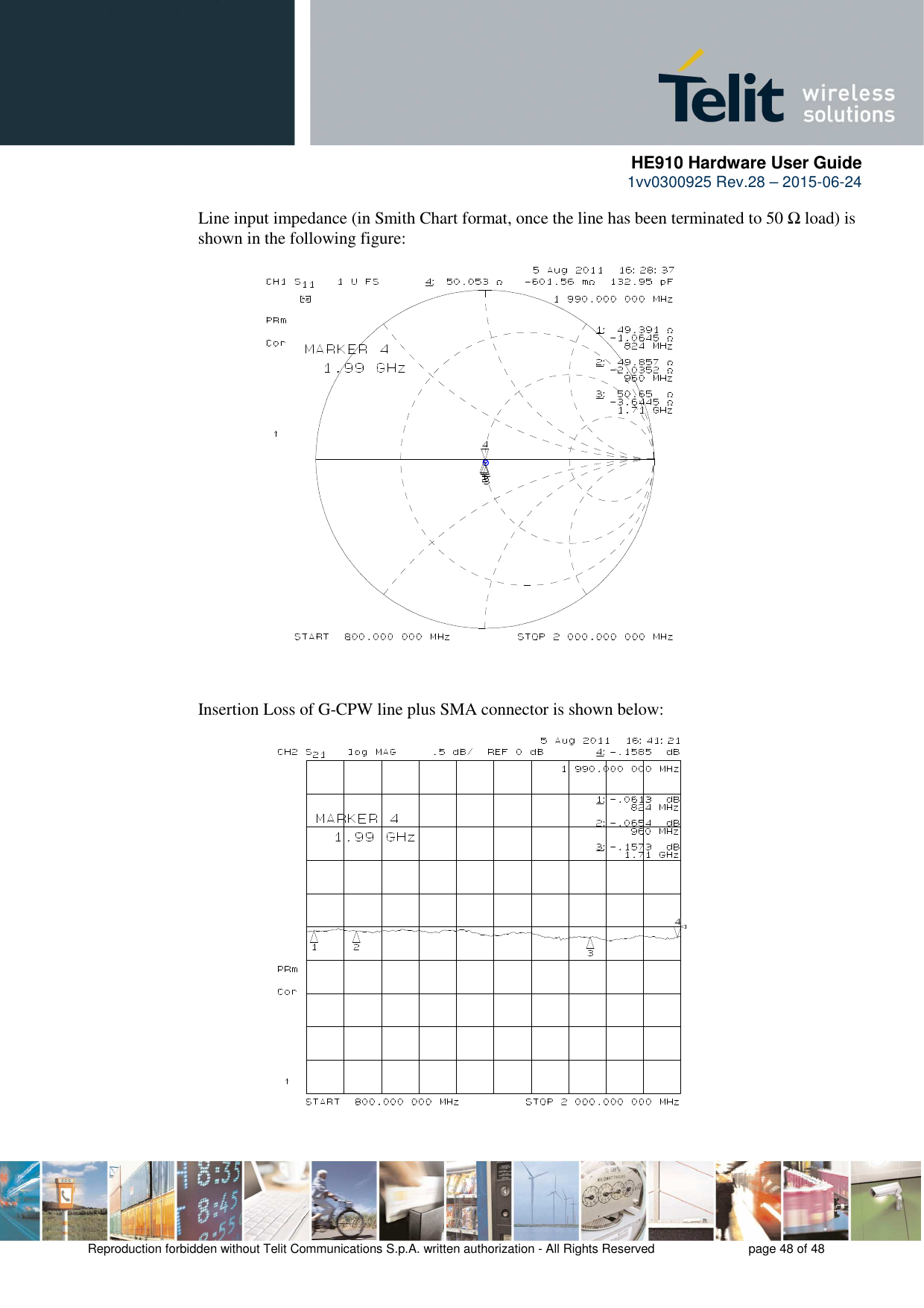
Telit Communications S p A HE910GL 2G/3.5G Module User Manual 1vv0300925 HE910 Hardware User Guide r28
Telit Communications S.p.A. 2G/3.5G Module 1vv0300925 HE910 Hardware User Guide r28
UserManual.wiki
>
Telit Communications S p A
>
HE910GL User Manual
User Manual
Navigation menu
Upload a User Manual
Namespaces
Wiki Guide
HTML
PDF
Info
Views
User Manual
Discussion / Help
Navigation


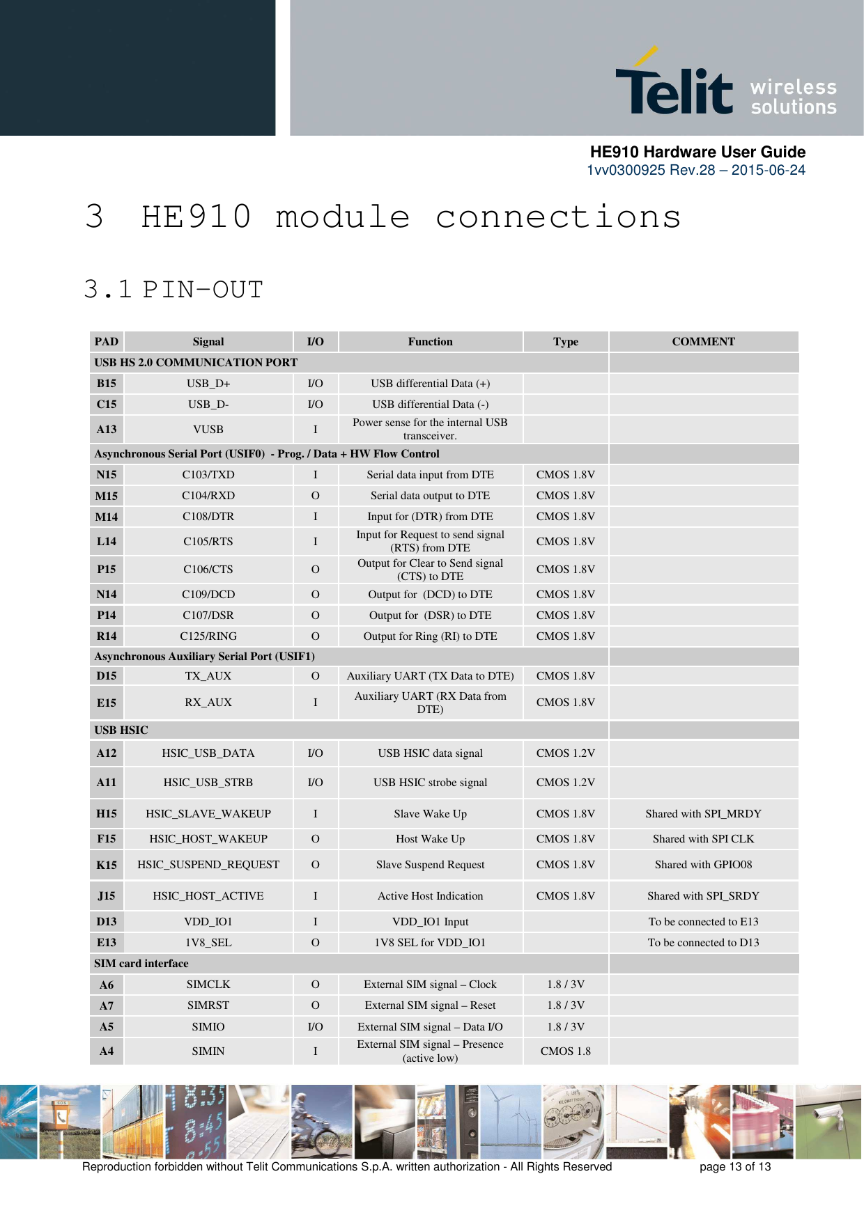
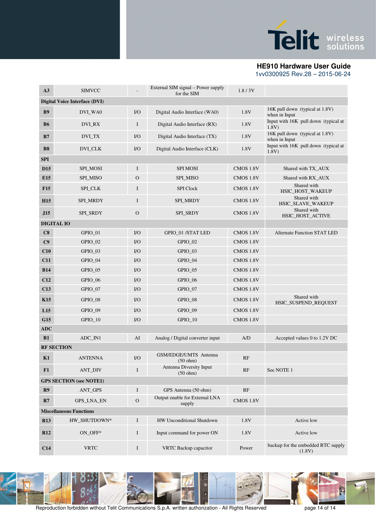
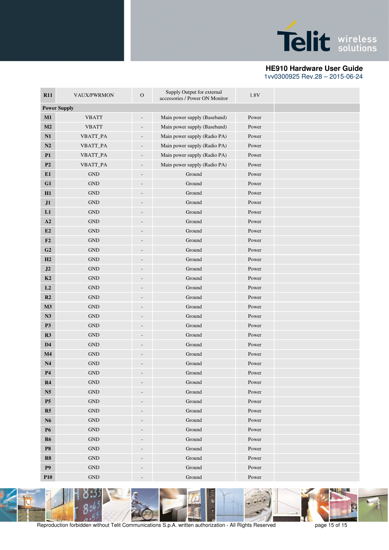
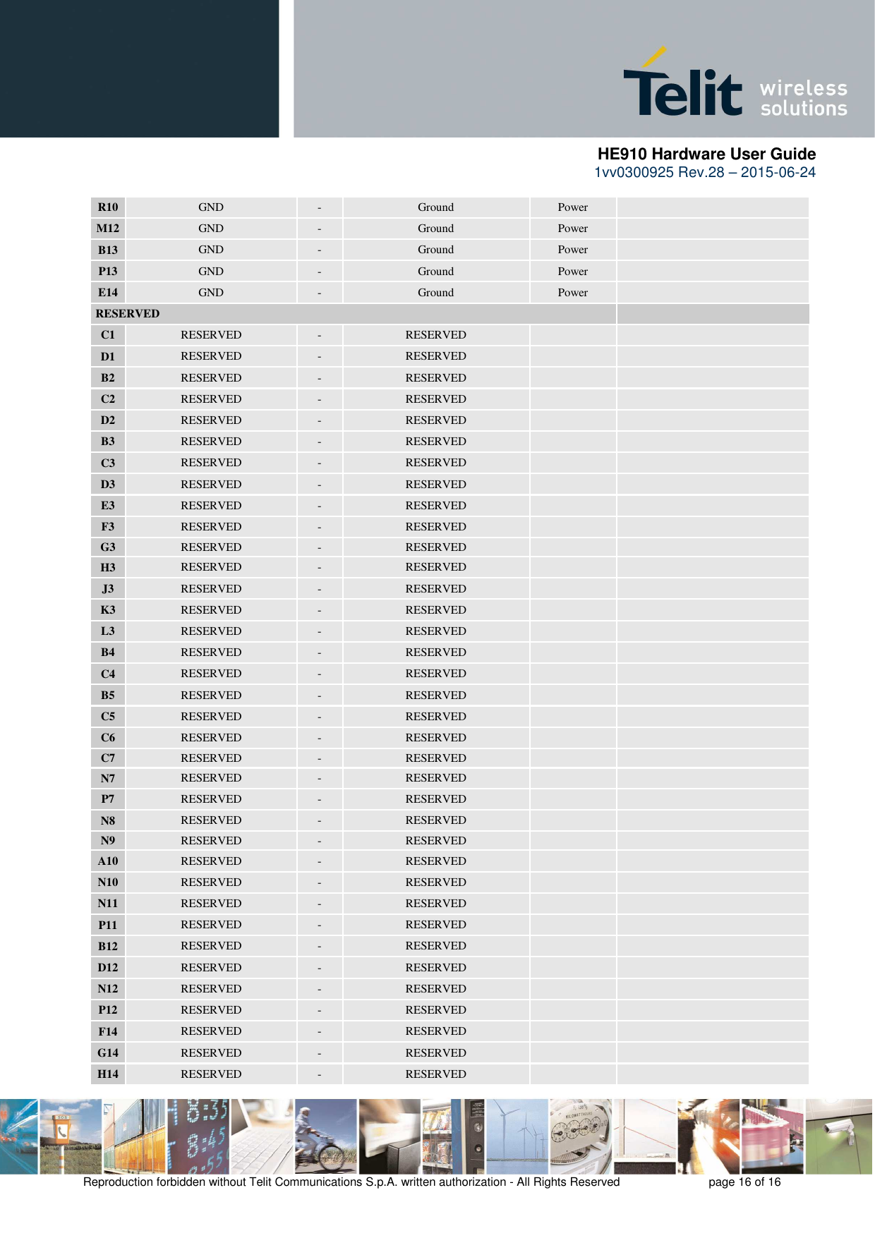


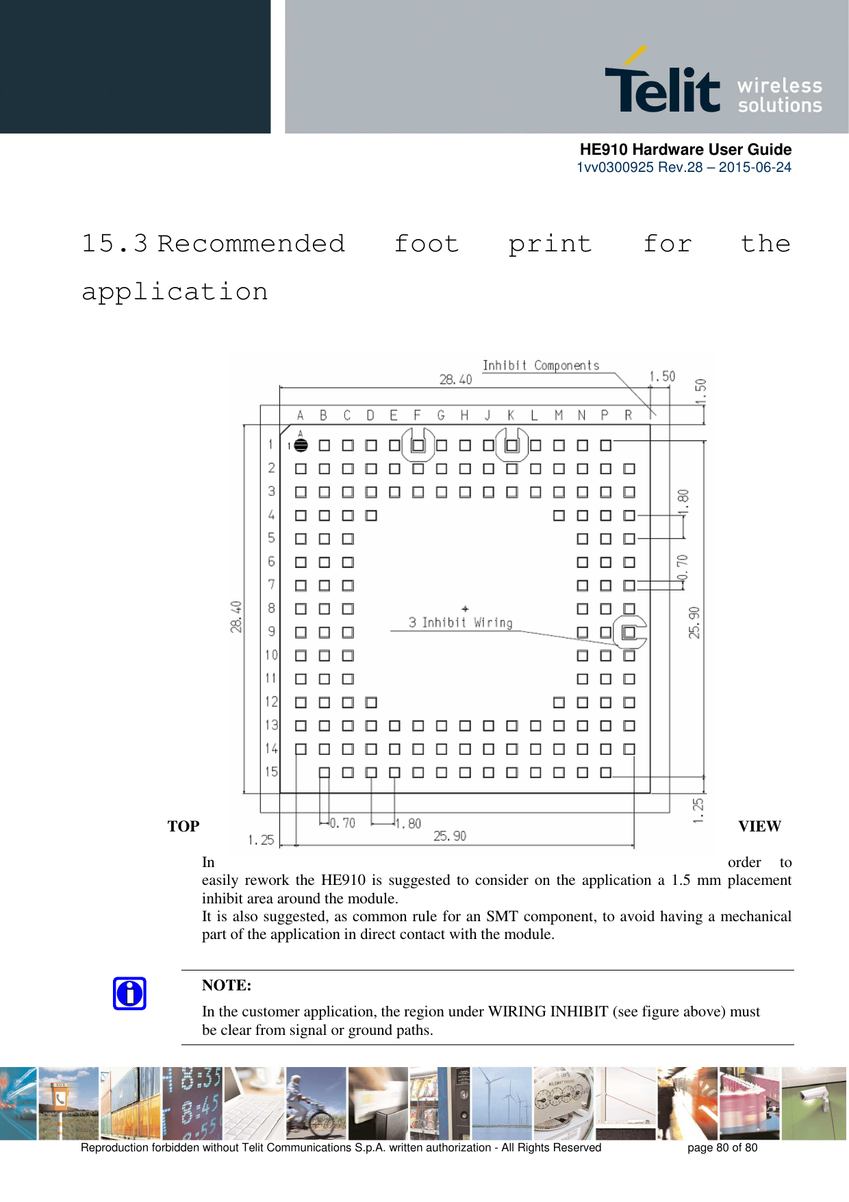
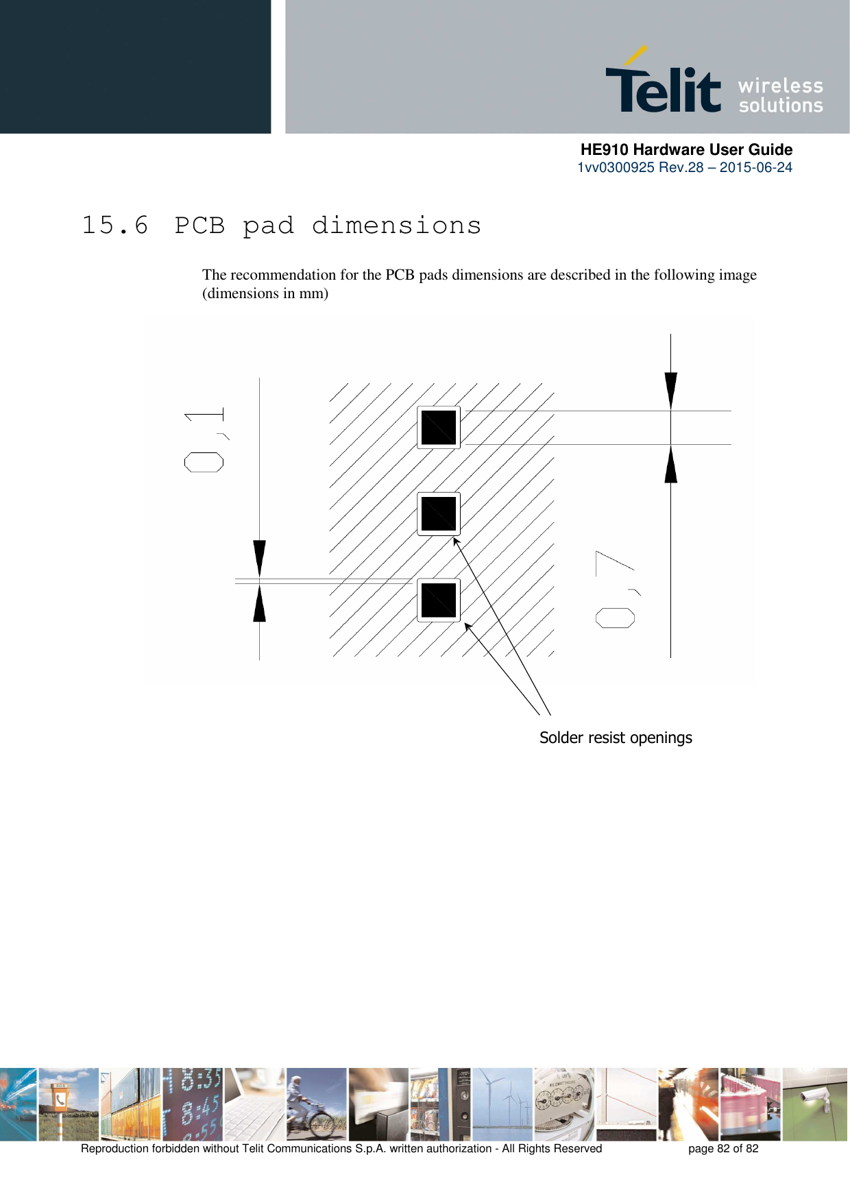
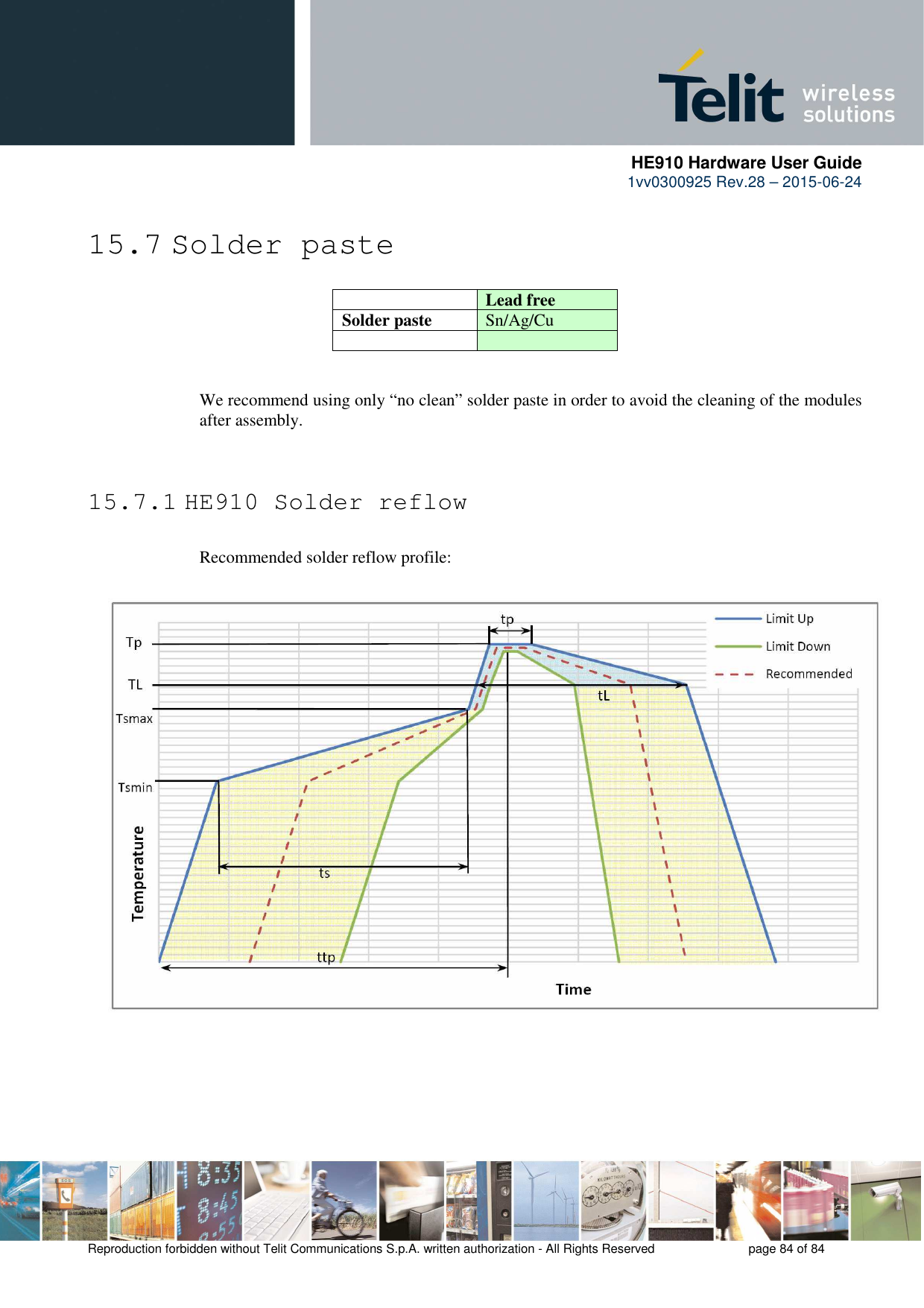
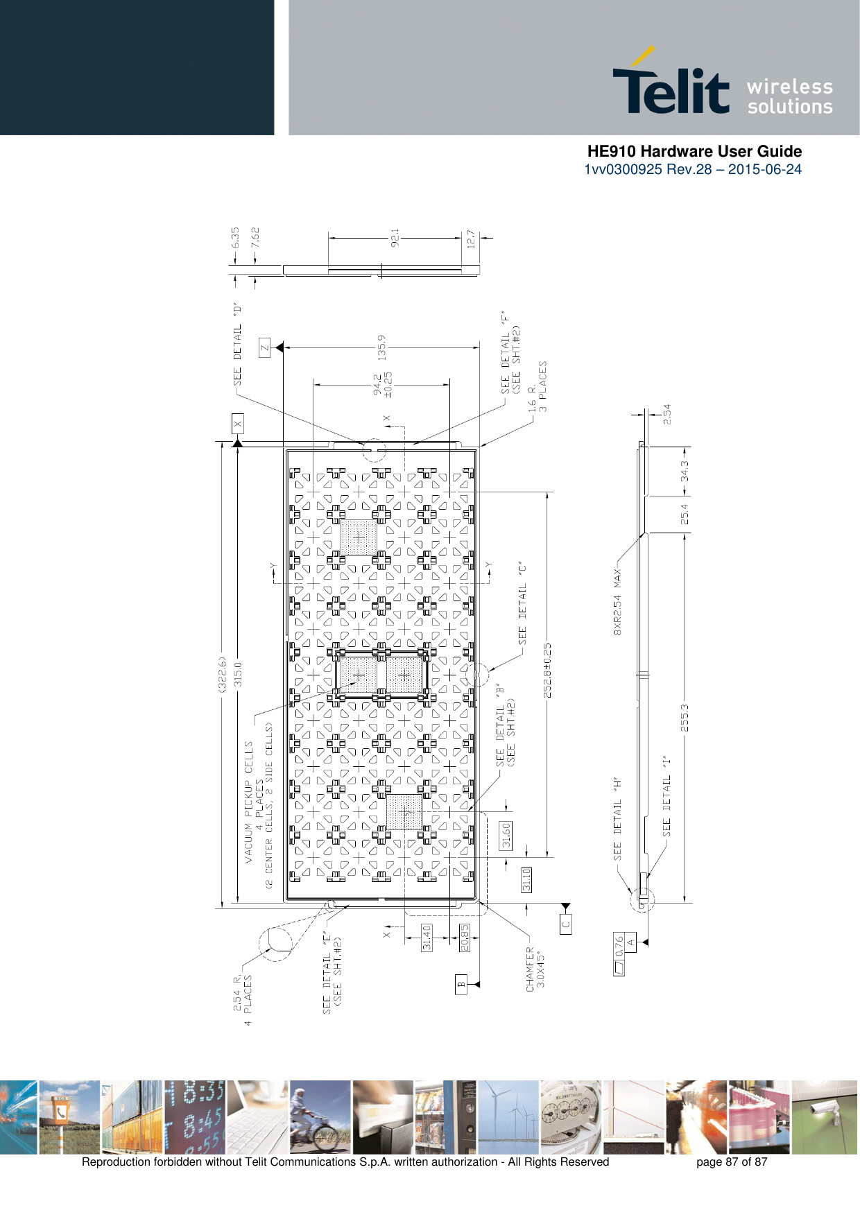
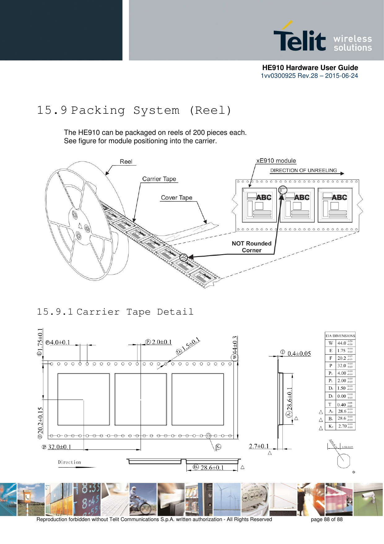
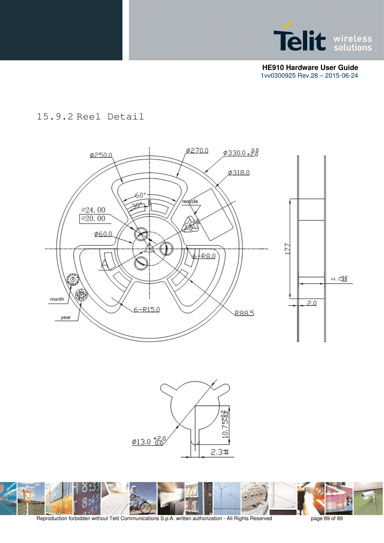
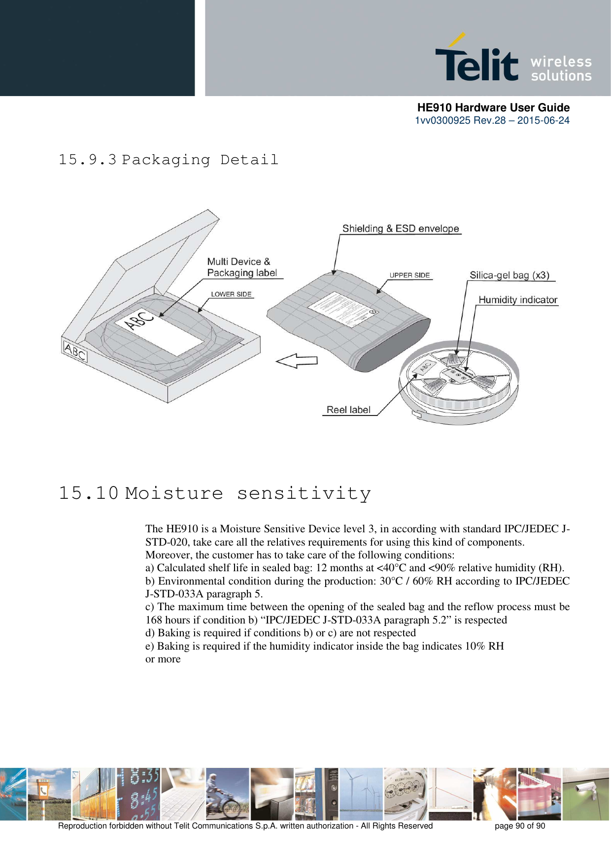
![HE910 Hardware User Guide 1vv0300925 Rev.28 – 2015-06-24 Reproduction forbidden without Telit Communications S.p.A. written authorization - All Rights Reserved page 83 of 83 It is not recommended to place via or micro-via not covered by solder resist in an area of 0,3 mm around the pads unless it carries the same signal of the pad itself (see following figure). Holes in pad are allowed only for blind holes and not for through holes. Recommendations for PCB pad surfaces: Finish Layer thickness [µm] Properties Electro-less Ni / Immersion Au 3 –7 / 0.05 – 0.15 good solder ability protection, high shear force values The PCB must be able to resist the higher temperatures which are occurring at the lead-free process. This issue should be discussed with the PCB-supplier. Generally, the wettability of tin-lead solder paste on the described surface plating is better compared to lead-free solder paste. It is not necessary to panel the application’s PCB, however in that case it is suggested to use milled contours and predrilled board breakouts; scoring or v-cut solutions are not recommended. Inhibit area for micro-via](https://usermanual.wiki/Telit-Communications-S-p-A/HE910GL/User-Guide-2667404-Page-83.png)