Telit Communications S p A HE910NAV2 2G/3.5G module, HE910-NAG V2, HE910-NA V2 User Manual HE910 V2 Hardware User Guide
Telit Communications S.p.A. 2G/3.5G module, HE910-NAG V2, HE910-NA V2 HE910 V2 Hardware User Guide
Contents
- 1. updated SW manual
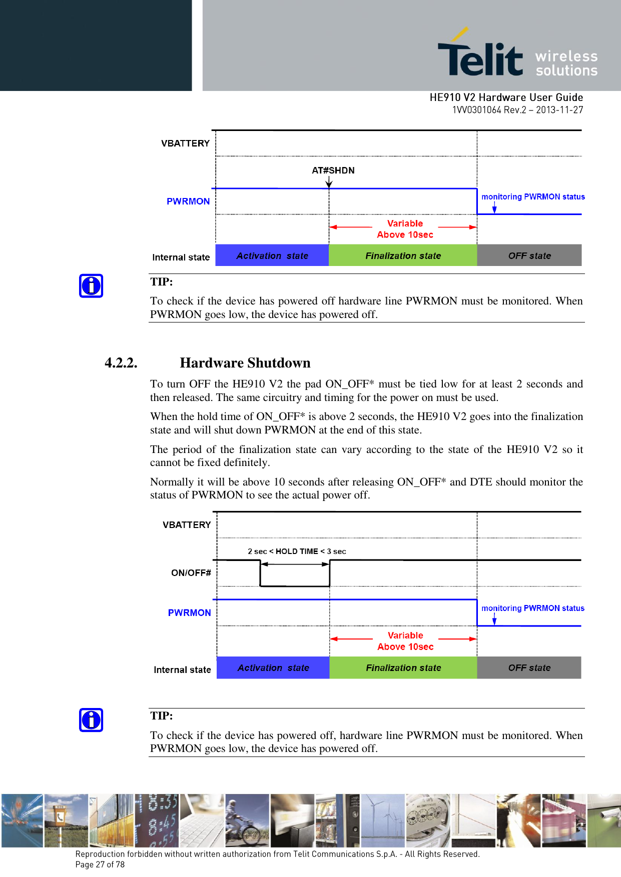
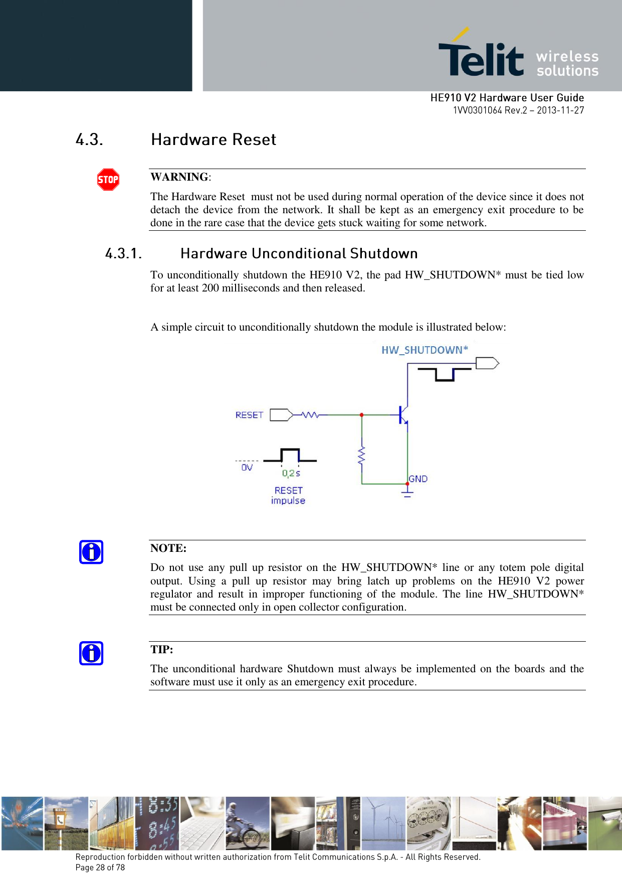
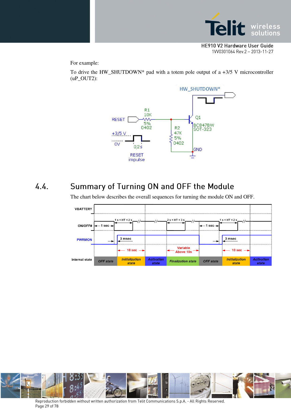
- 2. Updated Hardware manual
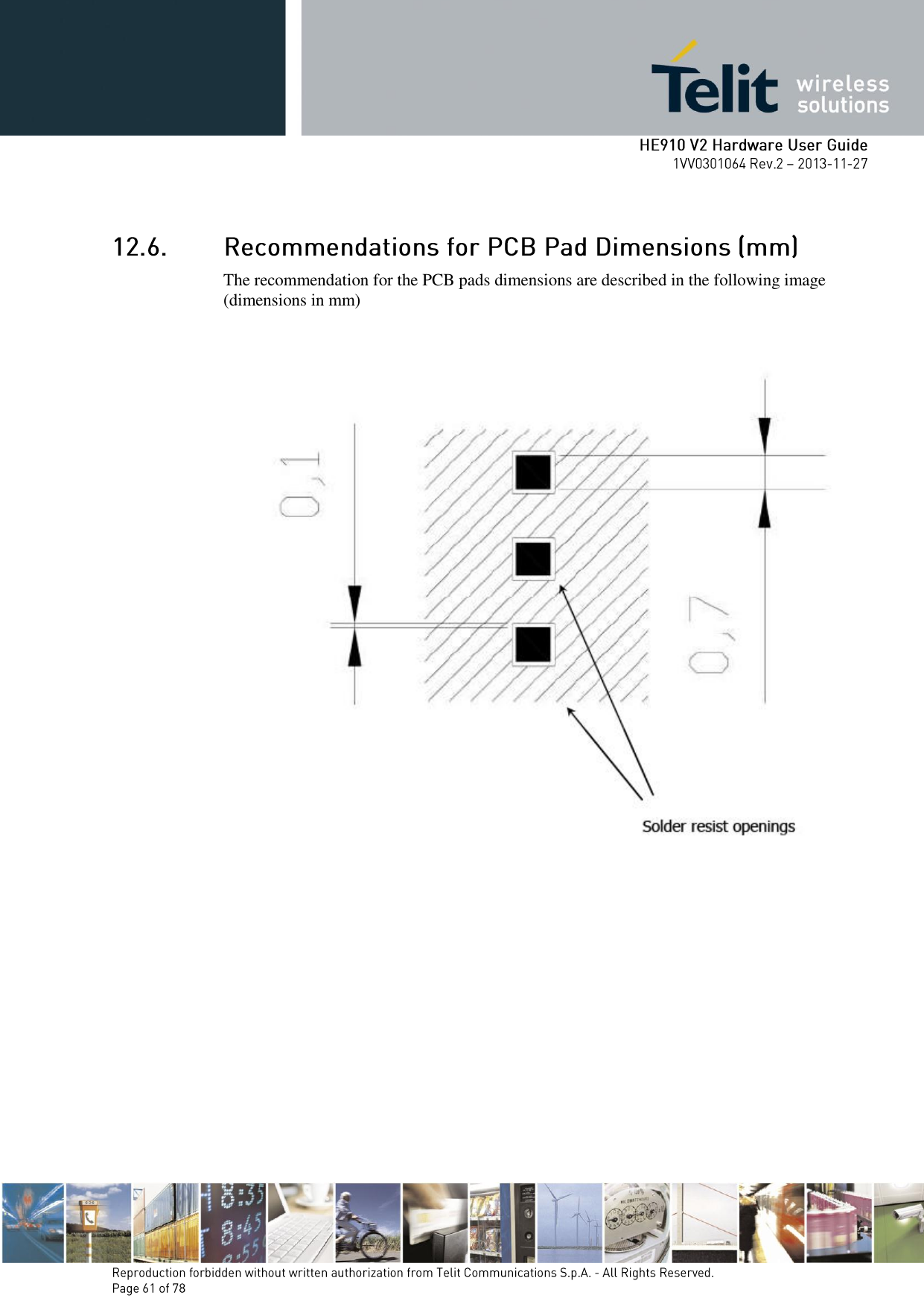
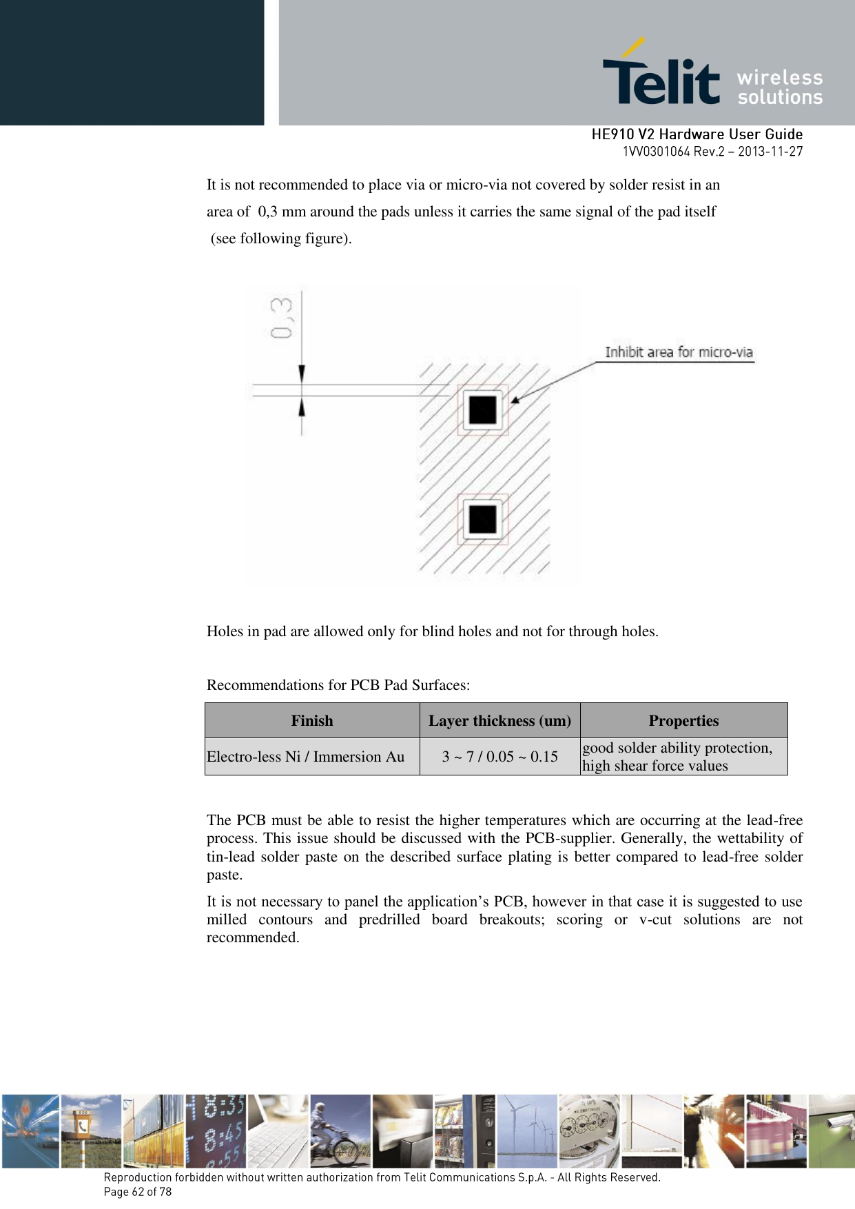
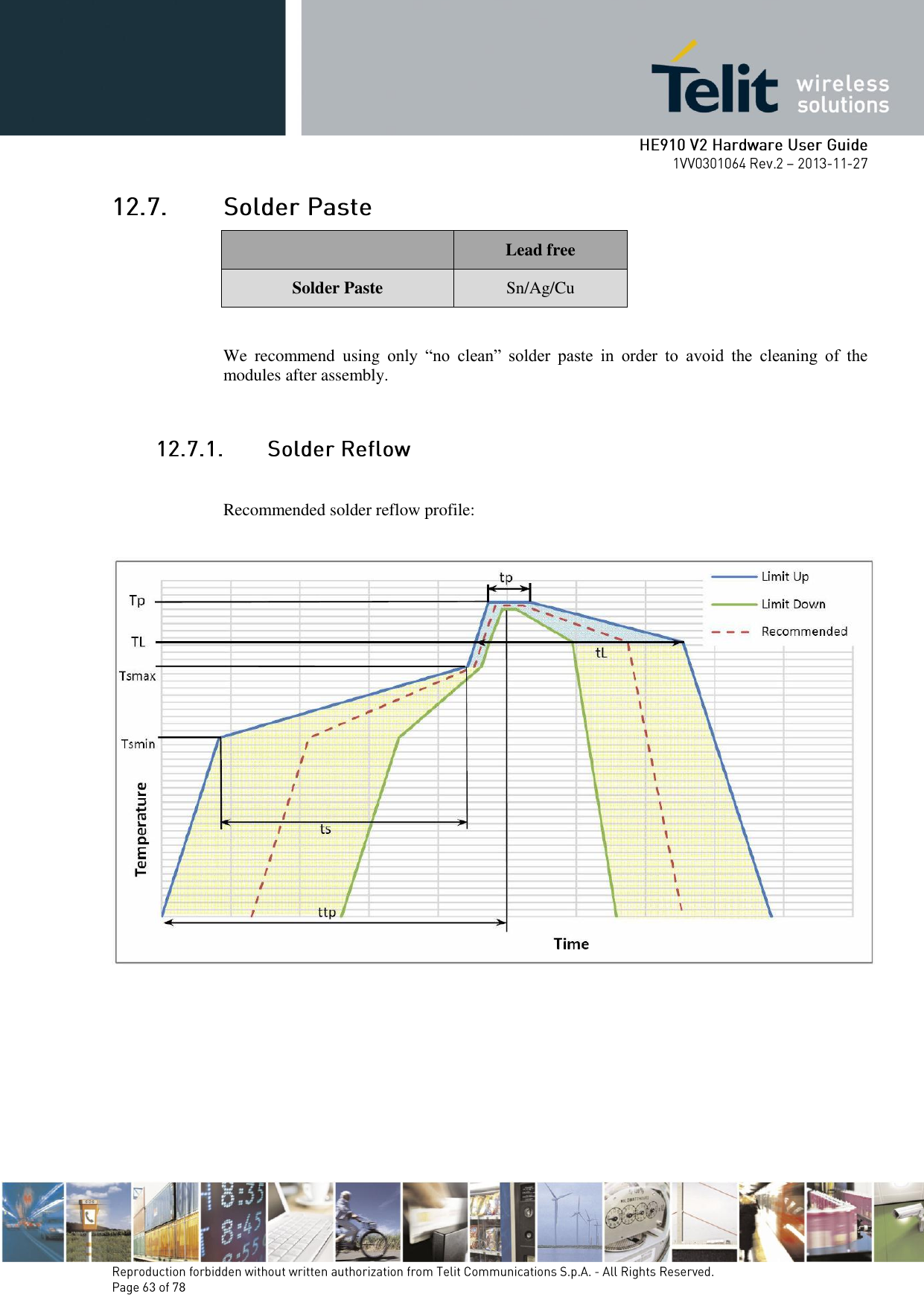
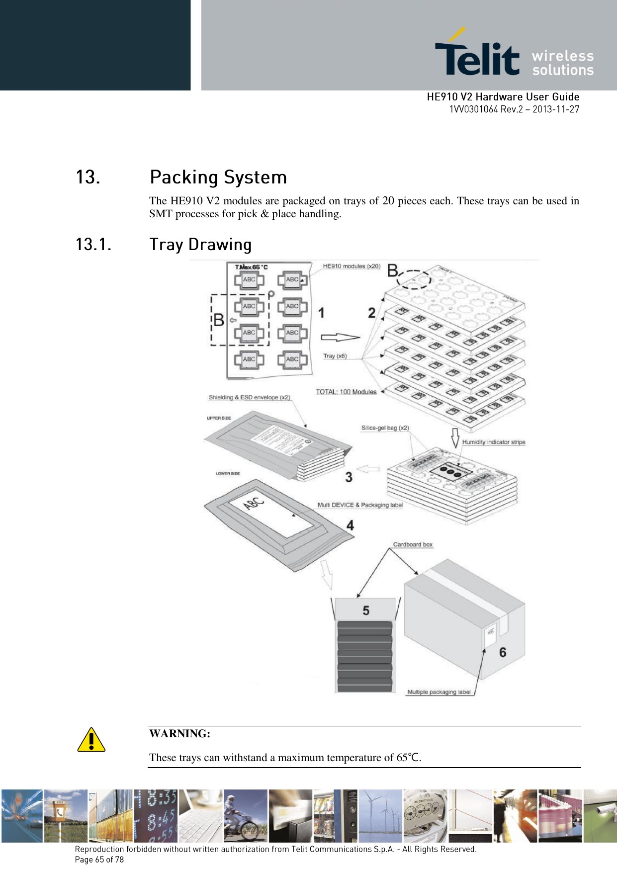
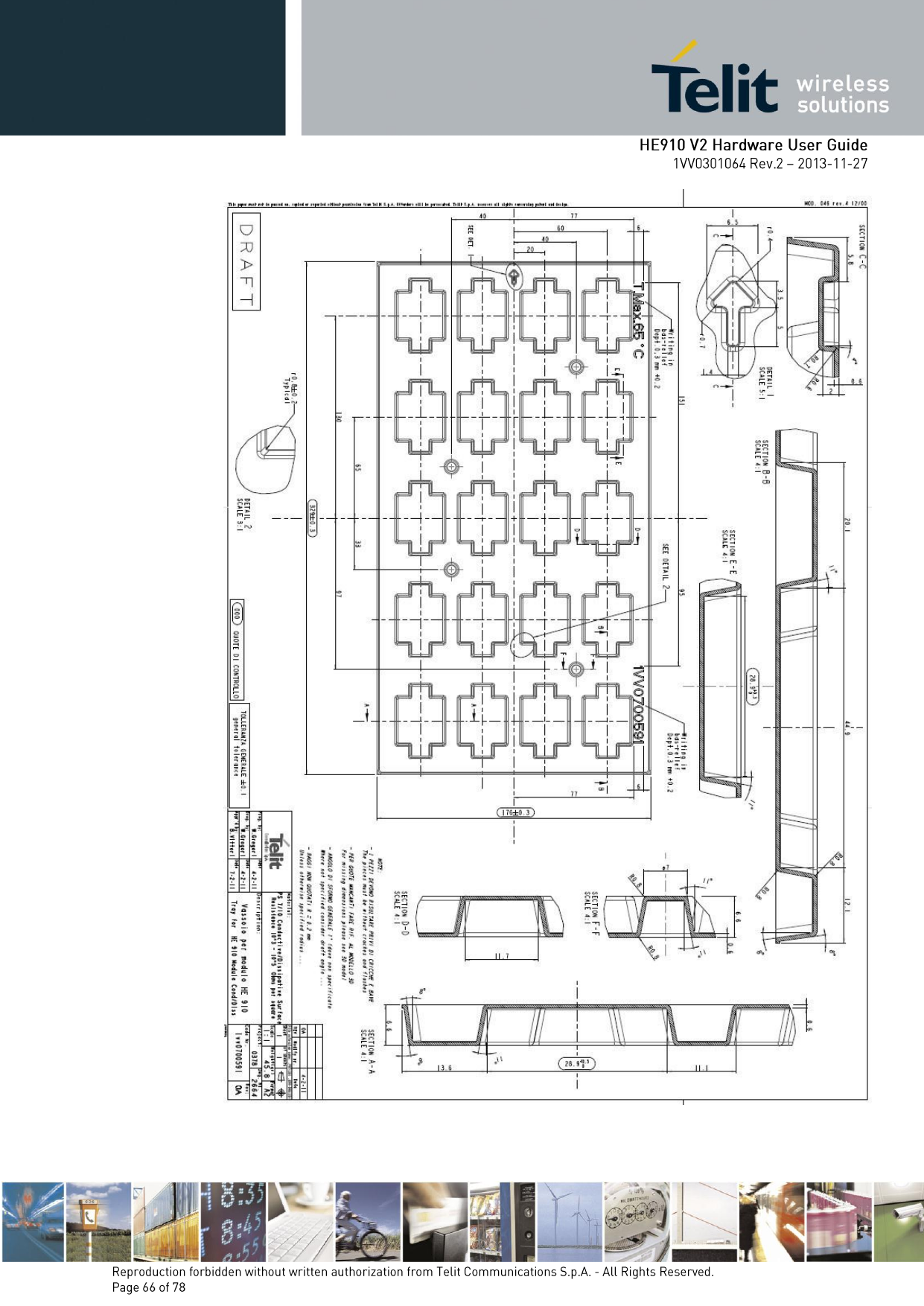
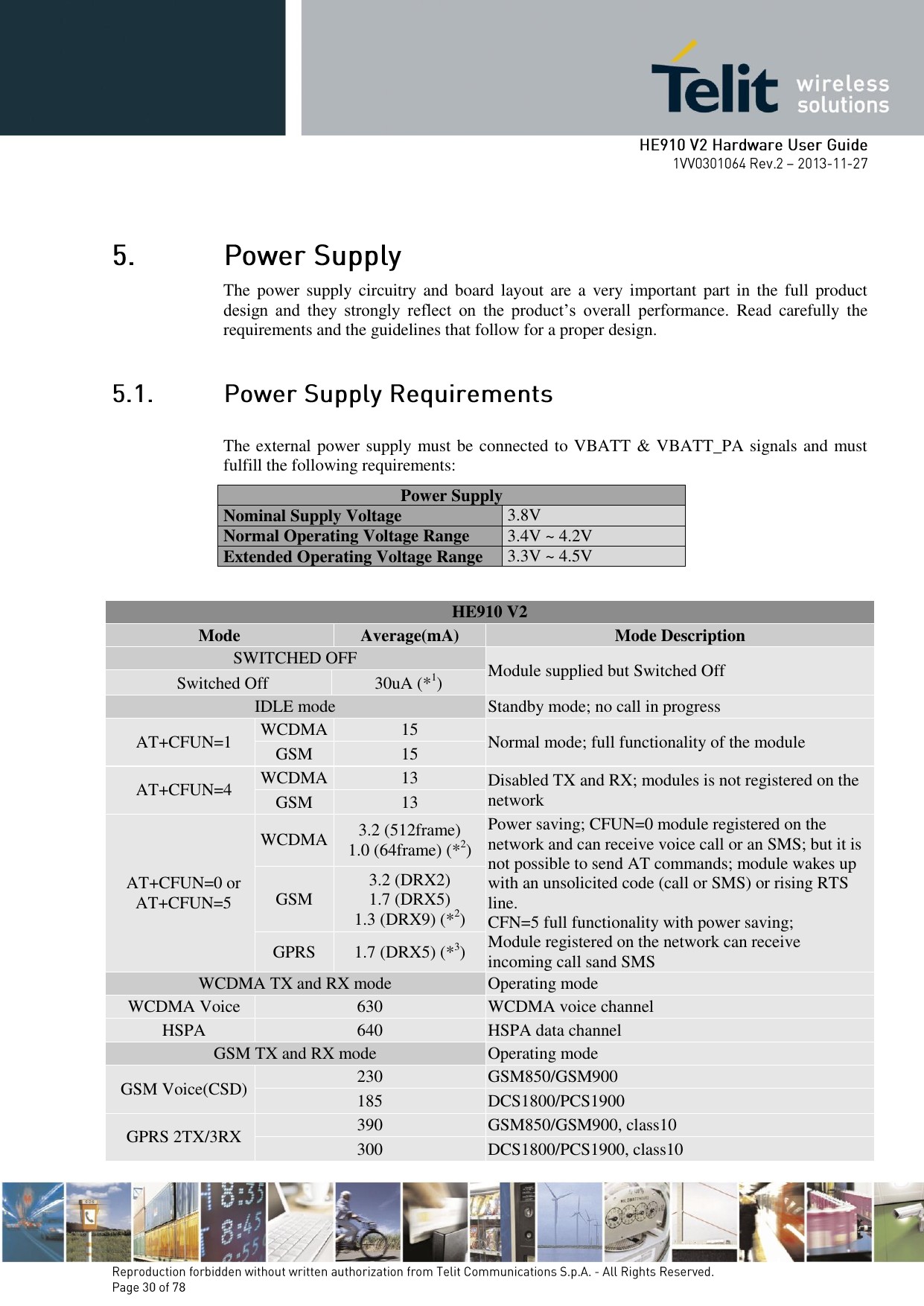
Updated Hardware manual


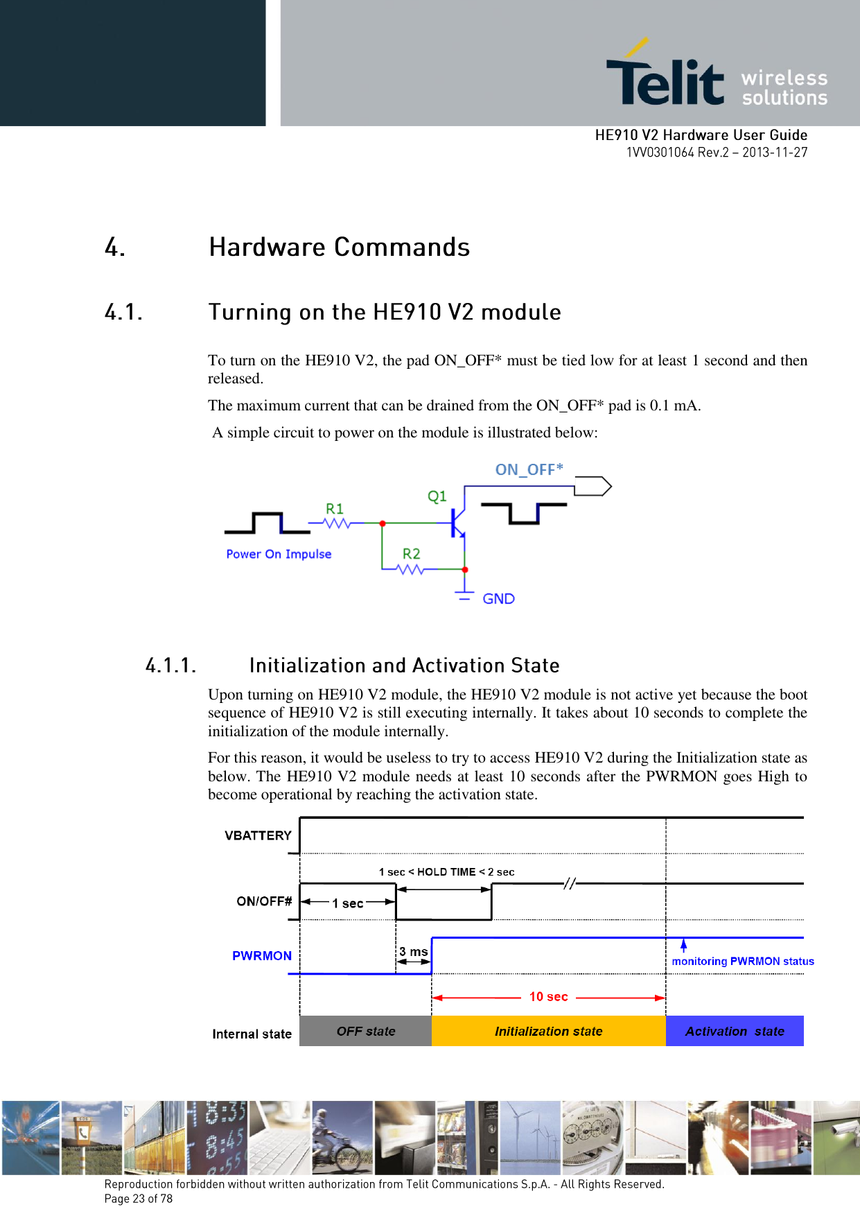
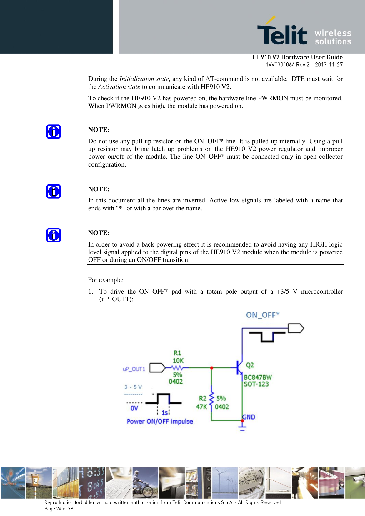
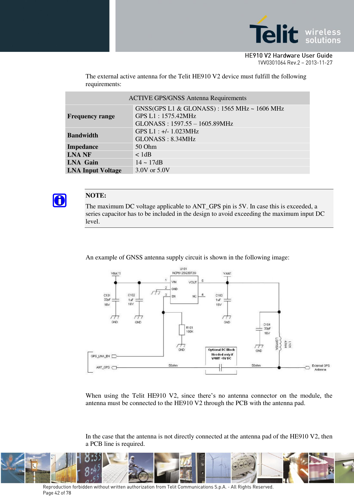

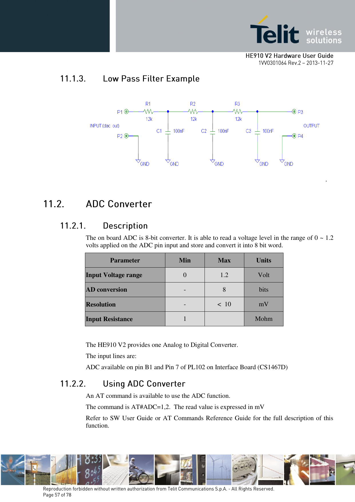
![The HE910 V2 module provides a Digital to Analog Converter. The signal (named DAC_OUT) is available on pin C13 of the HE910 V2 module and on pin 6 of PL302 on Interface Board (CS1467D). The on board DAC is in the range from 0 to 1023. However, an external low-pass filter is necessary. Parameter Min Max Units Voltage range (filtered) 0 1.8 Volt Range 0 1023 Steps The precision is 1023 steps, so since the maximum voltage is 2V, the integrated voltage could be calculated with the following formula: Integrated output voltage = 2 * value / 1023 DAC_OUT line must be integrated (for example with a low band pass filter) in order to obtain an analog voltage. An AT command is available to use the DAC function. The command is: AT#DAC[=<enable>[,<value>]] <value> - scale factor of the integrated output voltage (0..1023 ~ 10 bit precision) it must be present if <enable>=1 Refer to SW User Guide or AT Commands Reference Guide for the full description of this function. NOTE: The DAC frequency is selected internally. D/A converter must not be used during POWERSAVING.](https://usermanual.wiki/Telit-Communications-S-p-A/HE910NAV2.Updated-Hardware-manual/User-Guide-2159729-Page-56.png)