Telit Communications S p A LM940 LM940 User Manual User Guide
Telit Communications S.p.A. LM940 User Guide
UserManual.wiki
>
Telit Communications S p A
>
LM940 User Manual
User Guide
Navigation menu
Upload a User Manual
Namespaces
Wiki Guide
HTML
PDF
Info
Views
User Manual
Discussion / Help
Navigation
![[01.2017] Mod.0818 2017-01 Rev.0 LM940 HW Design Guide 1VV0301352 Rev. 2 –2017-07-19](https://usermanual.wiki/Telit-Communications-S-p-A/LM940/User-Guide-3476656-Page-1.png)
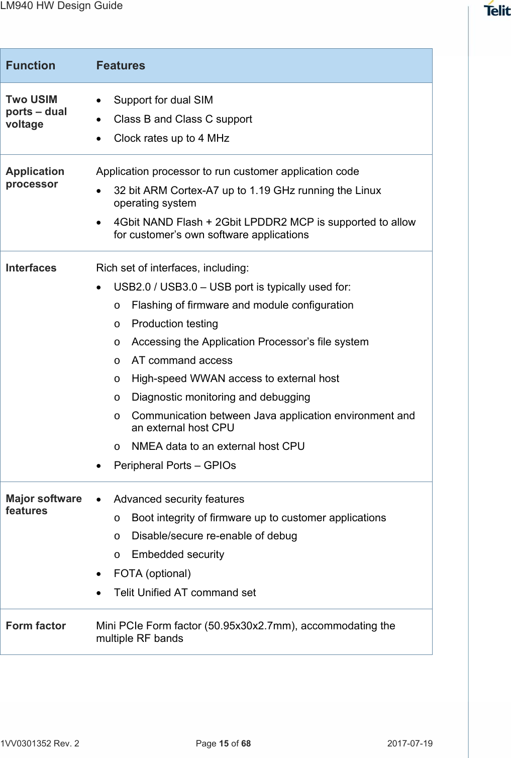
![LM940 HW Design Guide 1VV0301352 Rev. 2 Page 26 of 68 2017-07-19 4. POWER SUPPLY The power supply circuitry and board layout are very important parts of the full product design, with critical impact on the overall product performance. Read the following requirements and guidelines carefully to ensure a good and proper design. Power Supply Requirements The LM940 power requirements are as follows: Power Supply Requirements Nominal supply voltage 3.3V Supply voltage range 3.10V – 3.6V Maximum ripple on module input supply 30 mV Power Consumption Below table provides typical current consumption values of LM940 for various operation modes. LM940 Current Consumption Mode Average [Typ.] Mode Description IDLE Mode IDLE Mode 60.0 mA No call connection USB3.0 is connected to a host Operative Mode (LTE) LTE (22 dBm) 750 mA LTE data call (Non-CA BW 5MHz, RB=1) 1250 mA LTE data call (CA_3A+7A+20A, 20MHz+20MHz+20MHz, Full RB, 256QAM DL / 64QAM UL, FDD 600Mbps DL / 75Mbps UL) Operative Mode (WCDMA) WCDMA Voice 650 mA WCDMA voice call (Tx = 23 dBm)WCDMA HSPA (22 dBm) 650 mA WCDMA data call (DC-HSDPA up to 42 Mbps, Max Throughput) * Worst/best case current values depend on network configuration - not under module control. ** Applied MPR –2dB 16-QAM full RB *** 3.3 voltage / room temperature](https://usermanual.wiki/Telit-Communications-S-p-A/LM940/User-Guide-3476656-Page-26.png)
![LM940 HW Design Guide 1VV0301352 Rev. 2 Page 30 of 68 2017-07-19 Internal LDO for GNSS bias The LDO for GNSS bias is applied inside the LM940 model. The voltage supply come from LM940’s LDO to GNSS active antenna. This table lists the LDO for GNSS bias of LM940. LM940 Reference Voltage Symbol Parameter Min Typ Max Unit VGNSS DC bias Voltage of Internal LDO for GNSS bias 2.9 3.1 3.3 [V] IGNSS DC bias Current of Internal LDO for GNSS bias - - 50 [mA]](https://usermanual.wiki/Telit-Communications-S-p-A/LM940/User-Guide-3476656-Page-30.png)
![LM940 HW Design Guide 1VV0301352 Rev. 2 Page 31 of 68 2017-07-19 5. ELECTRICAL SPECIFICATIONS Absolute Maximum Ratings – Not Operational Caution – A deviation from the value ranges listed below may harm the LM940 module. Absolute Maximum Ratings – Not Operational Symbol Parameter Min Max Unit VBATT Battery supply voltage on pin VBATT -0.5 +4.0 [V] Recommended Operating Conditions Recommended Operating Conditions Symbol Parameter Min Typ Max Unit Tamb Ambient temperature -40 +25 +85 [°C] VBATT Battery supply voltage on pin VBATT 3.1 3.3 3.6 [V] IVBATT + IVBATT_PA Peak current to be used to dimension decoupling capacitors on pin VBATT - 80 2500 [mA]](https://usermanual.wiki/Telit-Communications-S-p-A/LM940/User-Guide-3476656-Page-31.png)
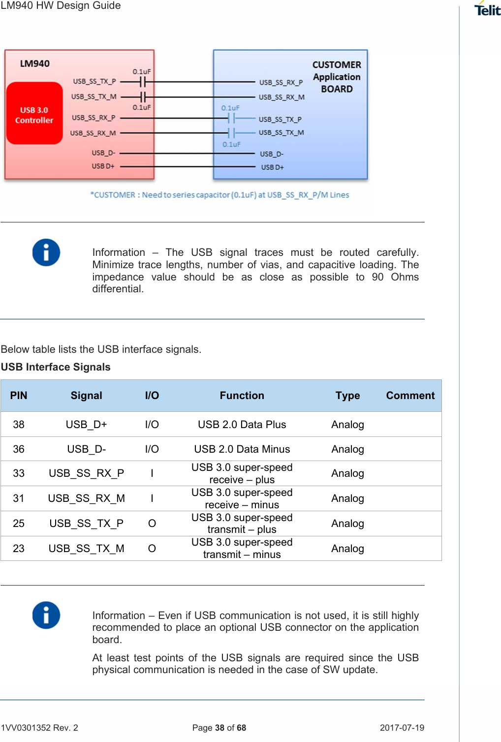
![LM940 HW Design Guide 1VV0301352 Rev. 2 Page 32 of 68 2017-07-19 6. DIGITAL SECTION Logic Levels Unless otherwise specified, all the interface circuits of the LM940 are 1.8V CMOS logic. Only USIM interfaces are capable of dual voltage I/O. The following tables show the logic level specifications used in the LM940 interface circuits. The data specified in the tables below is valid throughout all drive strengths and the entire temperature ranges. Caution – Do not connect LM940’s digital logic signal directly to OEM’s digital logic signal with a level higher than 2.3V for 1.8V CMOS signals. 6.1.1. 1.8V Pins – Absolute Maximum Ratings Absolute Maximum Ratings – Not Functional Parameter Min Max Input level on any digital pin when on -- +2.16V Input voltage on analog pins when on -- +2.16 V 6.1.2. 1.8V Standard GPIOs Operating Range – Interface Levels (1.8V CMOS) Parameter Min Max Unit Comment VIH Input high level 1.17V 2.1V [V] VIL Input low level -0.3V 0.63V [V] VOH Output high level 1.35V 1.8V [V] VOL Output low level 0V 0.45V [V] IIL Low-level input leakage current -1 -- [uA] No pull-up IIH High-level input leakage current -- 1 [uA] No pull-down IILPU Low-level input leakage current -97.5 -27.5 [uA] With pull-up](https://usermanual.wiki/Telit-Communications-S-p-A/LM940/User-Guide-3476656-Page-32.png)
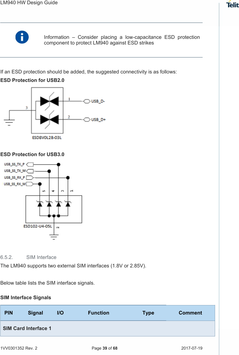
![LM940 HW Design Guide 1VV0301352 Rev. 2 Page 33 of 68 2017-07-19 Parameter Min Max Unit Comment IIHPD High-level input leakage current 27.5 97.5 [uA] With pull-down CI/o I/O capacitance -- 5 [pF] 6.1.3. 1.8V SIM Card Pins Operating Range – SIM Pins Working at 1.8V Parameter Min Max Unit Comment VIH Input high level 1.26V 2.1V [V] VIL Input low level -0.3V 0.36V [V] VOH Output high level 1.44V 1.8V [V] VOL Output low level 0V 0.4V [V] IIL Low-level input leakage current -- 1000 [uA] No pull-up IIH High-level input leakage current -20 20 [uA] No pull-down 6.1.4. 2.85V Pins – Absolute Maximum Ratings Absolute Maximum Ratings – Not Functional Parameter Min Max Input level on any digital pin when on -- +3.42V Input voltage on analog pins when on -- +3.42 V 6.1.5. SIM Card Pins @2.85V Operating Range – For SIM Pins Operating at 2.85V Parameter Min Max Unit Comment VIH Input high level 1.995V 3.15V [V] VIL Input low level -0.3V 0.57V [V] VOH Output high level 2.28V 2.85V [V] VOL Output low level 0V 0.4V [V]](https://usermanual.wiki/Telit-Communications-S-p-A/LM940/User-Guide-3476656-Page-33.png)
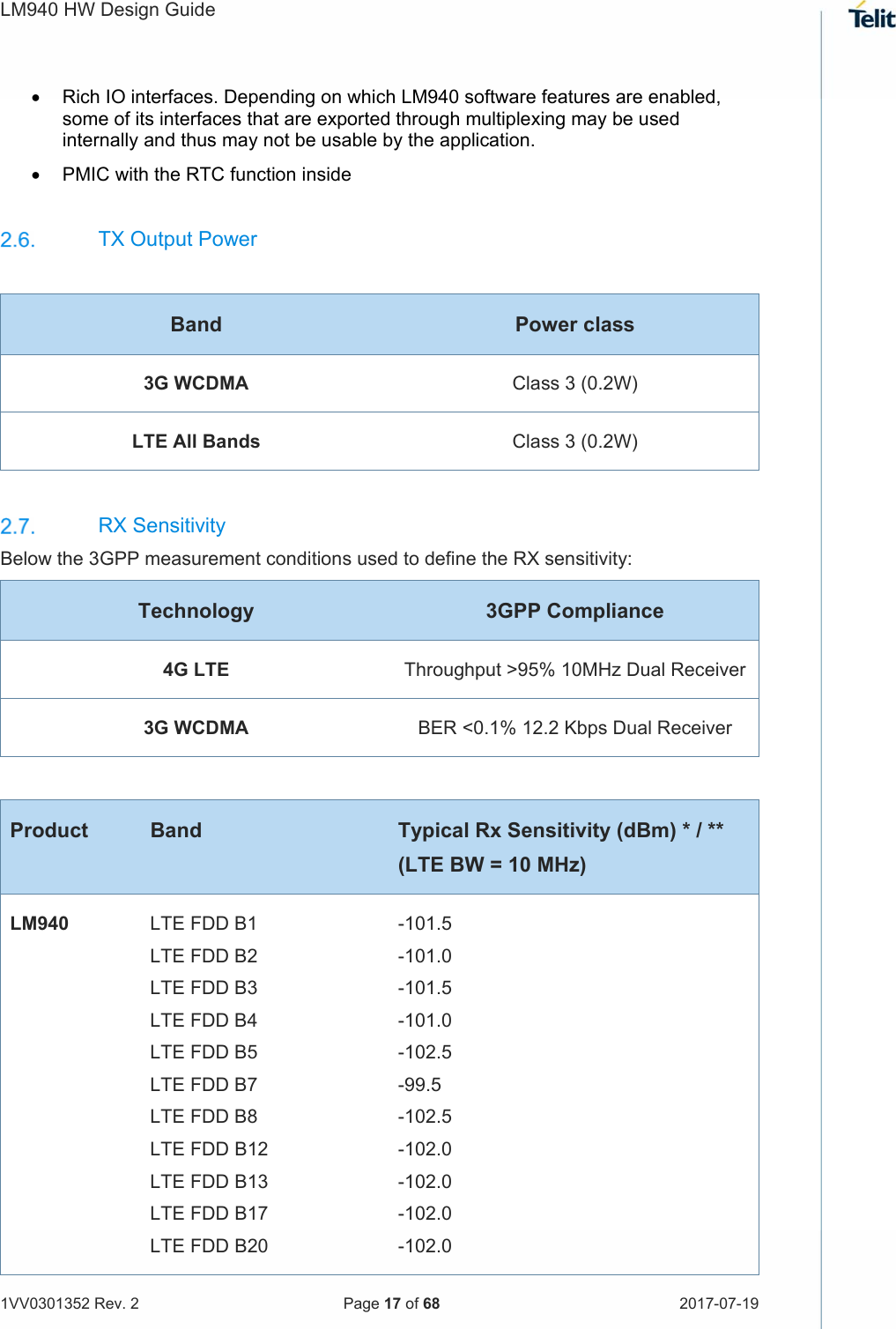
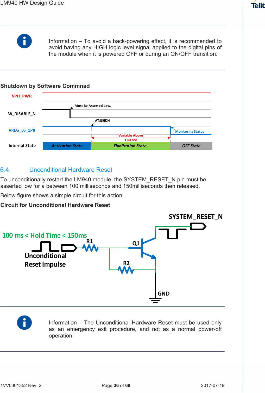
![LM940 HW Design Guide 1VV0301352 Rev. 2 Page 34 of 68 2017-07-19 Parameter Min Max Unit Comment IIL Low-level input leakage current -- 1000 [uA] No pull-up IIH High-level input leakage current -20 20 [uA] No pull-down Power On The LM940 is automatically turning on when the VBATT is supplied. Information – To turn on the LM940 module, the W_DISABLE_N pin must not be asserted low. 6.2.1. Initialization and Activation State After turning on the LM940 module, the LM940 is not yet activated because the SW initialization process of the LM940 module is still in process internally. It takes some time to fully complete the HW and SW initialization of the module. For this reason, it is impossible to access LM940 during the Initialization state. As shown in below figure, the LM940 becomes operational (in the Activation state) at least 15 seconds after the VBATT is supplied. LM940 Initialization and Activation InitializationState ActivationStateInternalStateVREG_L6_1P8W_DISABLE_NOFFStateTBDsecUSBDriverLoadedAllInterfacesAndPinsConfiguredVBATTTBDsec](https://usermanual.wiki/Telit-Communications-S-p-A/LM940/User-Guide-3476656-Page-34.png)
![[01.2017] Mod.0818 2017-01 Rev.0](https://usermanual.wiki/Telit-Communications-S-p-A/LM940/User-Guide-3476656-Page-68.png)