Telit Communications S p A LM940 LM940 User Manual User Guide
Telit Communications S.p.A. LM940 User Guide
User Guide

[01.2017]
Mod.0818 2017-01 Rev.0
LM940
HW Design Guide
1VV0301352 Rev. 2 –2017-07-19

LM940 HW Design Guide
1VV0301352 Rev. 2 Page 2 of 68 2017-07-19
SPECIFICATIONS ARE SUBJECT TO CHANGE WITHOUT NOTICE
NOTICE
While reasonable efforts have been made to assure the accuracy of this document, Telit
assumes no liability resulting from any inaccuracies or omissions in this document, or from
use of the information obtained herein. The information in this document has been carefully
checked and is believed to be reliable. However, no responsibility is assumed for
inaccuracies or omissions. Telit reserves the right to make changes to any products
described herein and reserves the right to revise this document and to make changes from
time to time in content hereof with no obligation to notify any person of revisions or changes.
Telit does not assume any liability arising out of the application or use of any product,
software, or circuit described herein; neither does it convey license under its patent rights
or the rights of others.
It is possible that this publication may contain references to, or information about Telit
products (machines and programs), programming, or services that are not announced in
your country. Such references or information must not be construed to mean that Telit
intends to announce such Telit products, programming, or services in your country.
COPYRIGHTS
This instruction manual and the Telit products described in this instruction manual may be,
include or describe copyrighted Telit material, such as computer programs stored in
semiconductor memories or other media. Laws in the Italy and other countries preserve for
Telit and its licensors certain exclusive rights for copyrighted material, including the
exclusive right to copy, reproduce in any form, distribute and make derivative works of the
copyrighted material. Accordingly, any copyrighted material of Telit and its licensors
contained herein or in the Telit products described in this instruction manual may not be
copied, reproduced, distributed, merged or modified in any manner without the express
written permission of Telit. Furthermore, the purchase of Telit products shall not be deemed
to grant either directly or by implication, estoppel, or otherwise, any license under the
copyrights, patents or patent applications of Telit, as arises by operation of law in the sale
of a product.
COMPUTER SOFTWARE COPYRIGHTS
The Telit and 3rd Party supplied Software (SW) products described in this instruction
manual may include copyrighted Telit and other 3rd Party supplied computer programs
stored in semiconductor memories or other media. Laws in the Italy and other countries
preserve for Telit and other 3rd Party supplied SW certain exclusive rights for copyrighted
computer programs, including the exclusive right to copy or reproduce in any form the
copyrighted computer program. Accordingly, any copyrighted Telit or other 3rd Party
supplied SW computer programs contained in the Telit products described in this instruction
manual may not be copied (reverse engineered) or reproduced in any manner without the
express written permission of Telit or the 3rd Party SW supplier. Furthermore, the purchase
of Telit products shall not be deemed to grant either directly or by implication, estoppel, or
otherwise, any license under the copyrights, patents or patent applications of Telit or other
3rd Party supplied SW, except for the normal non-exclusive, royalty free license to use that
arises by operation of law in the sale of a product.

LM940 HW Design Guide
1VV0301352 Rev. 2 Page 3 of 68 2017-07-19
USAGE AND DISCLOSURE RESTRICTIONS
I. License Agreements
The software described in this document is the property of Telit and its licensors. It is
furnished by express license agreement only and may be used only in accordance with the
terms of such an agreement.
II. Copyrighted Materials
Software and documentation are copyrighted materials. Making unauthorized copies is
prohibited by law. No part of the software or documentation may be reproduced,
transmitted, transcribed, stored in a retrieval system, or translated into any language or
computer language, in any form or by any means, without prior written permission of Telit
III. High Risk Materials
Components, units, or third-party products used in the product described herein are NOT
fault-tolerant and are NOT designed, manufactured, or intended for use as on-line control
equipment in the following hazardous environments requiring fail-safe controls: the
operation of Nuclear Facilities, Aircraft Navigation or Aircraft Communication Systems, Air
Traffic Control, Life Support, or Weapons Systems (High Risk Activities"). Telit and its
supplier(s) specifically disclaim any expressed or implied warranty of fitness for such High
Risk Activities.
IV. Trademarks
TELIT and the Stylized T Logo are registered in Trademark Office. All other product or
service names are the property of their respective owners.
V. Third Party Rights
The software may include Third Party Right software. In this case you agree to comply with
all terms and conditions imposed on you in respect of such separate software. In addition
to Third Party Terms, the disclaimer of warranty and limitation of liability provisions in this
License shall apply to the Third Party Right software.
TELIT HEREBY DISCLAIMS ANY AND ALL WARRANTIES EXPRESS OR IMPLIED
FROM ANY THIRD PARTIES REGARDING ANY SEPARATE FILES, ANY THIRD PARTY
MATERIALS INCLUDED IN THE SOFTWARE, ANY THIRD PARTY MATERIALS FROM
WHICH THE SOFTWARE IS DERIVED (COLLECTIVELY “OTHER CODE”), AND THE
USE OF ANY OR ALL THE OTHER CODE IN CONNECTION WITH THE SOFTWARE,
INCLUDING (WITHOUT LIMITATION) ANY WARRANTIES OF SATISFACTORY
QUALITY OR FITNESS FOR A PARTICULAR PURPOSE.
NO THIRD PARTY LICENSORS OF OTHER CODE SHALL HAVE ANY LIABILITY FOR
ANY DIRECT, INDIRECT, INCIDENTAL, SPECIAL, EXEMPLARY, OR CONSEQUENTIAL
DAMAGES (INCLUDING WITHOUT LIMITATION LOST PROFITS), HOWEVER CAUSED
AND WHETHER MADE UNDER CONTRACT, TORT OR OTHER LEGAL THEORY,
ARISING IN ANY WAY OUT OF THE USE OR DISTRIBUTION OF THE OTHER CODE
OR THE EXERCISE OF ANY RIGHTS GRANTED UNDER EITHER OR BOTH THIS
LICENSE AND THE LEGAL TERMS APPLICABLE TO ANY SEPARATE FILES, EVEN IF
ADVISED OF THE POSSIBILITY OF SUCH DAMAGES.

LM940 HW Design Guide
1VV0301352 Rev. 2 Page 4 of 68 2017-07-19
Applicability Table
PRODUCTS
LM940
LM940 HW Design Guide
1VV0301352 Rev. 2 Page 5 of 68 2017-07-19
Contents
NOTICE 2
COPYRIGHTS .................................................................................................. 2
COMPUTER SOFTWARE COPYRIGHTS ....................................................... 2
USAGE AND DISCLOSURE RESTRICTIONS ................................................ 3
APPLICABILITY TABLE .................................................................................. 4
CONTENTS ...................................................................................................... 5
1. INTRODUCTION ............................................................................ 9
Scope ............................................................................................. 9
Audience ........................................................................................ 9
Contact Information, Support ......................................................... 9
Text Conventions ......................................................................... 11
Related Documents ...................................................................... 12
2. GENERAL PRODUCT DESCRIPTION ........................................ 13
Overview ...................................................................................... 13
Product Variants and Frequency Bands ....................................... 13
2.2.1. RF Bands per Regional Variant .................................................... 13
Target market ............................................................................... 14
Main features ................................................................................ 14
Block Diagram .............................................................................. 16
TX Output Power .......................................................................... 17
RX Sensitivity ............................................................................... 17
Mechanical specifications ............................................................. 18
2.8.1. Dimensions ................................................................................... 18
2.8.2. Weight .......................................................................................... 18
Environmental Requirements ....................................................... 18
2.9.1. Temperature Range ..................................................................... 18
2.9.2. RoHS Compliance ........................................................................ 19
3. PINS ALLOCATION .................................................................... 20
Pin-out .......................................................................................... 20
LM940 Signals That Must Be Connected ..................................... 24
Pin Layout .................................................................................... 25
LM940 HW Design Guide
1VV0301352 Rev. 2 Page 6 of 68 2017-07-19
4. POWER SUPPLY ........................................................................ 26
Power Supply Requirements ........................................................ 26
Power Consumption ..................................................................... 26
General Design Rules .................................................................. 27
4.3.1. Electrical Design Guidelines ......................................................... 27
4.3.1.1. + 5V Input Source Power Supply – Design Guidelines ................ 27
4.3.2. Thermal Design Guidelines .......................................................... 27
4.3.3. Power Supply PCB layout Guidelines .......................................... 28
RTC .............................................................................................. 29
Reference Voltage ........................................................................ 29
Internal LDO for GNSS bias ......................................................... 30
5. ELECTRICAL SPECIFICATIONS ................................................ 31
Absolute Maximum Ratings – Not Operational ............................. 31
Recommended Operating Conditions .......................................... 31
6. DIGITAL SECTION ...................................................................... 32
Logic Levels ................................................................................. 32
6.1.1. 1.8V Pins – Absolute Maximum Ratings ...................................... 32
6.1.2. 1.8V Standard GPIOs ................................................................... 32
6.1.3. 1.8V SIM Card Pins ...................................................................... 33
6.1.4. 2.85V Pins – Absolute Maximum Ratings .................................... 33
6.1.5. SIM Card Pins @2.85V ................................................................ 33
Power On ..................................................................................... 34
6.2.1. Initialization and Activation State .................................................. 34
Power Off ..................................................................................... 35
Unconditional Hardware Reset ..................................................... 36
Communication ports ................................................................... 37
6.5.1. USB Interface ............................................................................... 37
6.5.2. SIM Interface ................................................................................ 39
6.5.2.1. SIM Schematic Example .............................................................. 40
6.5.3. Control Signals ............................................................................. 41
6.5.3.1. W_DISABLE_N ............................................................................ 41
6.5.3.2. WAKE_N ...................................................................................... 41
6.5.3.3. WAN_LED_N ............................................................................... 42
6.5.4. General Purpose I/O .................................................................... 42
6.5.4.1. Using a GPIO Pin as Input ........................................................... 43
6.5.4.2. Using a GPIO Pin as Output ........................................................ 43
6.5.5. I2C – Inter-integrated circuit ......................................................... 43
LM940 HW Design Guide
1VV0301352 Rev. 2 Page 7 of 68 2017-07-19
Using the Temperature Monitor Function ..................................... 44
7. RF SECTION ................................................................................ 45
Antenna requirements .................................................................. 45
Main Antenna Requirements ........................................................ 45
Antenna Diversity Requirements .................................................. 45
GNSS Receiver ............................................................................ 46
7.4.1. GNSS RF Front End Design......................................................... 46
Antenna connection ...................................................................... 47
7.5.1. Antenna Connector ...................................................................... 47
7.5.2. Antenna Cable .............................................................................. 48
7.5.3. Antenna Installation Guidelines .................................................... 48
8. AUDIO SECTION ......................................................................... 50
Audio Interface ............................................................................. 50
Digital Audio ................................................................................. 50
9. MECHANICAL DESIGN............................................................... 51
General ......................................................................................... 51
Finishing & Dimensions ................................................................ 51
Drawing ........................................................................................ 51
10. APPLICATION GUIDE ................................................................. 52
Debug of the LM940 Module in Production .................................. 52
Bypass Capacitor on Power Supplies .......................................... 52
EMC Recommendations .............................................................. 53
11. PACKAGING ............................................................................... 56
Tray .............................................................................................. 56
12. CONFORMITY ASSESSMENT ISSUES ..................................... 58
Approvals ..................................................................................... 58
Declaration of Conformity ............................................................. 58
FCC certificates ............................................................................ 58
IC certificates ................................................................................ 58
FCC/IC Regulatory notices ........................................................... 58
13. SAFETY RECOMMENDATIONS ................................................. 62
READ CAREFULLY ..................................................................... 62
14. REFERENCE TABLE OF RF BANDS CHARACTERISTICS ..... 63
15. ACRONYMS ................................................................................ 65

LM940 HW Design Guide
1VV0301352 Rev. 2 Page 8 of 68 2017-07-19
16. DOCUMENT HISTORY ................................................................ 67

LM940 HW Design Guide
1VV0301352 Rev. 2 Page 9 of 68 2017-07-19
1. INTRODUCTION
Scope
This document introduces the Telit LM940 module and presents possible and
recommended hardware solutions for developing a product based on the LM940 module.
All the features and solutions detailed in this document are applicable to all LM940 variants,
where “LM940” refers to the variants listed in the Applicability Table.
If a specific feature is applicable to a specific product only, it will be clearly marked.
Information – LM940 refers to all modules listed in the Applicability
Table.
This document takes into account all the basic functions of a wireless module; a valid
hardware solution is suggested for each function, and incorrect solutions and common
errors to be avoided are pointed out.
Obviously, this document cannot embrace every hardware solution or every product that
can be designed. Where the suggested hardware configurations need not be considered
mandatory, the information given should be used as a guide and a starting point for properly
developing your product with the Telit LM940 module.
Information – The integration of the WCDMA/HSPA+/LTE LM940
cellular module within a user application must be done according to
the design rules described in this manual.
Audience
This document is intended for Telit customers, especially system integrators, about to
implement their applications using the Telit LM940 module.
Contact Information, Support
For general contact, technical support services, technical questions and report
documentation errors contact Telit Technical Support at:
TS-EMEA@telit.com
TS-AMERICAS@telit.com
TS-APAC@telit.com
TS-SRD@telit.com

LM940 HW Design Guide
1VV0301352 Rev. 2 Page 10 of 68 2017-07-19
Alternatively, use:
http://www.telit.com/en/products/technical-support-center/contact.php
For detailed information about where you can buy the Telit modules or for recommendations
on accessories and components visit:
http://www.telit.com
To register for product news and announcements or for product questions contact Telit’s
Technical Support Center (TTSC).
Our aim is to make this guide as helpful as possible. Keep us informed of your comments
and suggestions for improvements.
Telit appreciates feedback from the users of our information.
LM940 HW Design Guide
1VV0301352 Rev. 2 Page 11 of 68 2017-07-19
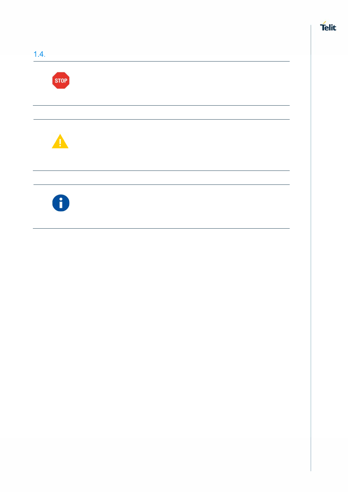
Text Conventions
Danger – This information MUST be followed or catastrophic
equipment failure or bodily injury may occur.
Caution or Warning – Alerts the user to important points about
integrating the module, if these points are not followed, the module and
end user equipment may fail or malfunction.
Tip or Information – Provides advice and suggestions that may be
useful when integrating the module.
All dates are in ISO 8601 format, i.e. YYYY-MM-DD.

LM940 HW Design Guide
1VV0301352 Rev. 2 Page 12 of 68 2017-07-19
Related Documents
LM940 SW User Guide, 1VV0301343
LM940 AT Commands Reference Guide, 80545ST10791A
Generic EVB HW User Guide, 1VV0301249
LM940 Interface Board HW User Guide, 1VV0301384
SIM Integration Design Guide Application Note Rev10, 80000NT10001A
Antenna Detection Application Note, 80000NT10002A

LM940 HW Design Guide
1VV0301352 Rev. 2 Page 13 of 68 2017-07-19
2. GENERAL PRODUCT DESCRIPTION
Overview
The aim of this document is to present possible and recommended hardware solutions
useful for developing a product with the Telit LM940 Mini PCIe module.
LM940 is Telit’s platform for Mini PCIe module for applications, such as M2M applications,
industrial mobile router and table PC, based on the following technologies:
LTE / WCDMA networks for data communication
Designed for industrial grade quality
In its most basic use case, LM940 can be applied as a wireless communication front-end
for mobile router products, offering mobile communication features to an external host
CPU through its rich interfaces.
LM940 can further support customer software applications and security features. LM940
provides a software application development environment with sufficient system resources
for creating rich on-board applications. Thanks to a dedicated application processor and
embedded security resources, product developers and manufacturers can create products
that guarantee fraud prevention and tamper evidence without extra effort for additional
security precautions.
LM940 is available in hardware variants as listed in Applicability Table
The designated RF band sets per each variant are detailed in Section 2.2, Product
Variants and Frequency Bands.
Product Variants and Frequency Bands
The operating frequencies in LTE & WCDMA modes conform to the 3GPP specifications.
2.2.1. RF Bands per Regional Variant
This table summarizes the LM940, showing the supported band sets and the supported
band pairs and triple for carrier aggregation.
RF Bands and Carrier Aggregation
LTE FDD LTE TDD HSPA+
Bands 1, 2, 3, 4, 5, 7, 8, 12, 13, 17, 20, 25, 26, 28, 29,
30, 66
38, 40, 41 1, 2, 4, 5, 8
GNSS GPS, GLONASS, BeiDou, Galileo
LTE 2DL carrier aggregation combinations
North
America
B2+B2, B2+B4, B2+B5, B2+B12, B2+B13, B2+B17, B2+B29, B2+B30,
B4+B4, B4+B5, B4+B7, B4+B12, B4+B13, B4+B17, B4+B29, B4+B30,
B5+B30, B12+B12, B12+B30, B25+B25, B25+B26, B25+B41, B26+B41,
B29+B30, B41+B41
Europe B1+B20, B3+B3, B3+B7, B3+B20, B3+B38, B7+B7, B7+B8, B7+B20,
B38+B38

LM940 HW Design Guide
1VV0301352 Rev. 2 Page 14 of 68 2017-07-19
Australia B1+B3, B1+B7, B1+B28, B3+B8, B3+B28, B5+B7, B5+B40, B7+B8,
B7+B20
LTE 3DL carrier aggregation combinations
North
America
B2+B2+B12/17, B2+B2+B13, B2+B2+B4, B2+B4+B5, B2+B4+B12,
B2+B4+B13, B2+B4+B29, B2+B5+B30, B2+B12+B12, B2+B12+B30,
B2+B29+B30, B4+B4+B5, B4+B4+B7, B4+B4+B12, B4+B4+B13,
B4+B5+B30, B4+B12+B12, B4+B12+B30, B4+B29+B30, B25+B26+B41,
B25+B41+B41, B26+B41+B41, B41+B41+B41
Europe B1+B3+B20, B1+B7+B20, B3+B3+B7, B3+B3+B20, B3+B7+B20,
B3+B7+B7, B3+B20+B38, B3+B38+B38
Australia B3+B3+B5, B3+B3+B8, B3+B7+B7, B3+B7+B28, B7+B7+B28,
B28+B40+B40, B40+B40+B40
Refer to Chapter 13 for details information about frequencies and bands.
Target market
LM940 can be used for telematics applications where tamper-resistance, confidentiality,
integrity, and authenticity of end-user information are required, for example:
Mobile router
Industrial equipment
Home network
Internet connectivity
Main features
The LM940 family of industrial grade cellular modules features LTE and multi-RAT module
together with an on-chip powerful application processor and a rich set of interfaces.
The major functions and features are listed below.
Main Features
Function Features
Module Multi-RAT cellular module for data communication
o LTE FDD/TDD Cat11(600/75 Mbps DL/UL)
o WCDMA up to DC HSPA+, Rel.9
Support for GPS, GLONASS, BeiDou, Galileo
Audio
subsystem
Support digital audio interface (optional)

LM940 HW Design Guide
1VV0301352 Rev. 2 Page 15 of 68 2017-07-19
Function Features
Two USIM
ports – dual
voltage
Support for dual SIM
Class B and Class C support
Clock rates up to 4 MHz
Application
processor
Application processor to run customer application code
32 bit ARM Cortex-A7 up to 1.19 GHz running the Linux
operating system
4Gbit NAND Flash + 2Gbit LPDDR2 MCP is supported to allow
for customer’s own software applications
Interfaces Rich set of interfaces, including:
USB2.0 / USB3.0 – USB port is typically used for:
o Flashing of firmware and module configuration
o Production testing
o Accessing the Application Processor’s file system
o AT command access
o High-speed WWAN access to external host
o Diagnostic monitoring and debugging
o Communication between Java application environment and
an external host CPU
o NMEA data to an external host CPU
Peripheral Ports – GPIOs
Major software
features
Advanced security features
o Boot integrity of firmware up to customer applications
o Disable/secure re-enable of debug
o Embedded security
FOTA (optional)
Telit Unified AT command set
Form factor Mini PCIe Form factor (50.95x30x2.7mm), accommodating the
multiple RF bands
LM940 HW Design Guide
1VV0301352 Rev. 2 Page 16 of 68 2017-07-19
Function Features
Environment
and quality
requirements
The entire module is designed and qualified by Telit for satisfying the
environment and quality requirements for use in applications
1
.
Single supply
module
The module generates all its internal supply voltages.
RTC The real-time clock is supported.
Operating
temperature
Range -40 °C to +85 °C
(conditions as defined in Section 2.9.1, Temperature Range)
Block Diagram
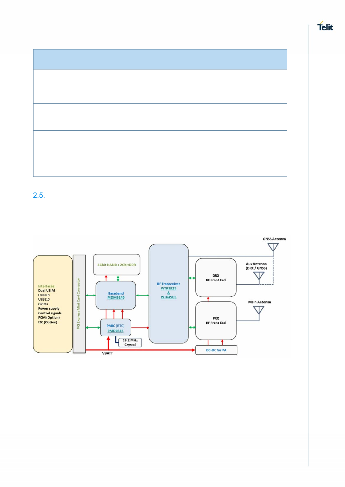
Below figure shows an overview of the internal architecture of the LM940 module.
LM940 Block Diagram
It includes the following sub-functions:
Application processor, Module subsystem and Location processing with their
external interfaces. These three functions are contained in a single SOC.
RF front end
1
InaccordancewithTelit’sRobustnessValidation,usingAEC‐Q100‐definedqualificationtests

LM940 HW Design Guide
1VV0301352 Rev. 2 Page 17 of 68 2017-07-19
Rich IO interfaces. Depending on which LM940 software features are enabled,
some of its interfaces that are exported through multiplexing may be used
internally and thus may not be usable by the application.
PMIC with the RTC function inside
TX Output Power
Band Power class
3G WCDMA Class 3 (0.2W)
LTE All Bands Class 3 (0.2W)
RX Sensitivity
Below the 3GPP measurement conditions used to define the RX sensitivity:
Technology 3GPP Compliance
4G LTE Throughput >95% 10MHz Dual Receiver
3G WCDMA BER <0.1% 12.2 Kbps Dual Receiver
Product Band Typical Rx Sensitivity (dBm) * / **
(LTE BW = 10 MHz)
LM940
LTE FDD B1
LTE FDD B2
LTE FDD B3
LTE FDD B4
LTE FDD B5
LTE FDD B7
LTE FDD B8
LTE FDD B12
LTE FDD B13
LTE FDD B17
LTE FDD B20
-101.5
-101.0
-101.5
-101.0
-102.5
-99.5
-102.5
-102.0
-102.0
-102.0
-102.0

LM940 HW Design Guide
1VV0301352 Rev. 2 Page 18 of 68 2017-07-19
LTE FDD B25
LTE FDD B26
LTE FDD B28
LTE FDD B30
LTE FDD B66
LTE TDD B38
LTE TDD B40
LTE TDD B41
-101.0
-102.0
-102.0
-100.5
-101.0
-100.0
-100.0
-99.5
LM940 WCDMA FDD B1
WCDMA FDD B2
WCDMA FDD B4
WCDMA FDD B5
WCDMA FDD B8
-108.5
-108.5
-108.5
-109.5
-109.5
* LTE Rx Sensitivity shall be verified by using both (all) antenna ports simultaneously.
** 3.3 Voltage / Room temperature
Mechanical specifications
2.8.1. Dimensions
The LM940 module’s overall dimensions are:
Length: 50.95 mm, +/- 0.15 mm tolerance
Width: 30.00 mm, +/- 0.15 mm tolerance
Thickness: 2.70 mm, +/- 0.15 mm tolerance
2.8.2. Weight
The nominal weight of the LM940 module is 9.6 gram.
Environmental Requirements
2.9.1. Temperature Range
Note
Operating
Temperature Range
–20°C ~ +55°C This range is defined by 3GPP (the global
standard for wireless mobile communication).
Telit guarantees its modules to comply with all
the 3GPP requirements and to have full
functionality of the module with in this range.

LM940 HW Design Guide
1VV0301352 Rev. 2 Page 19 of 68 2017-07-19
Note
–40°C ~ +85°C Telit guarantees full functionality within this
range as well. However, there may possibly
be some performance deviations in this
extended range relative to 3GPP
requirements, which means that some RF
parameters may deviate from the 3GPP
specification in the order of a few dB. For
example: receiver sensitivity or maximum
output power may be slightly degraded.
Even so, all the functionalities, such as call
connection, SMS, USB communication,
UART activation etc., will be maintained, and
the effect of such degradations will not lead to
malfunction.
Storage and non-
operating
Temperature Range
–40°C ~ +85°C
2.9.2. RoHS Compliance
As a part of the Telit corporate policy of environmental protection, the LM940 complies
with the RoHS (Restriction of Hazardous Substances) directive of the European Union
(EU directive 2011/65/EU).

LM940 HW Design Guide
1VV0301352 Rev. 2 Page 20 of 68 2017-07-19
3. PINS ALLOCATION
Pin-out
LM940 Pin-out
Pin Signal I/O Function Type Comment
USB HS 2.0 Communication Port
38 USB_D+ I/O USB 2.0 Data Plus Analog
36 USB_D- I/O USB 2.0 Data Minus Analog
USB SS 3.0 Communication Port
25 USB_SS_TX_P O USB 3.0 super-
speed transmit –
plus
Analog
23 USB_SS_TX_M O USB 3.0 super-
speed transmit –
minus
Analog
33 USB_SS_RX_P I USB 3.0 super-
speed receive – plus
Analog
31 USB_SS_RX_M I USB 3.0 super-
speed receive –
minus
Analog
SIM Card Interface 1
8 SIMVCC1 O Supply output for an
external UIM1 card
1.8V /
2.85V
Power
10 SIMIO1 I/O Data connection with
an external UIM1
card
1.8V /
2.85V
12 SIMCLK1 O Clock output to an
external UIM1 card
1.8V /
2.85V
14 SIMRST1 O Reset output to an
external UIM1 card
1.8V /
2.85V

LM940 HW Design Guide
1VV0301352 Rev. 2 Page 21 of 68 2017-07-19
SIM Card Interface 2
13 SIMVCC2 O Supply output for an
external UIM2 card
1.8 / 2.85V Power
19 SIMIO2 I/O Data connection with
an external UIM2
card
1.8 / 2.85V
17 SIMCLK2 O Clock output to an
external UIM2 card
1.8 / 2.85V
7 SIMRST2 O Reset output to an
external UIM2 card
1.8 / 2.85V
Digital I/O (GPIOs)
3 GPIO_01 I/O General purpose
I/O, SIMIN1
depending on
product
1.8V
5 GPIO_02 I/O General purpose
I/O, SIMIN2
depending on
product
1.8V
44 GPIO_03 I/O General purpose I/O 1.8V
46 GPIO_04 I/O General purpose I/O 1.8V
Control Signal
1 WAKE_N O Host wake-up 1.8V
20 W_DISABLE_N I RF disable 1.8V
42 WAN_LED_N O LED control 1.8V
Miscellaneous Functions
11 VREG_L6_1P8 O Reference Voltage 1.8V Power

LM940 HW Design Guide
1VV0301352 Rev. 2 Page 22 of 68 2017-07-19
22 SYSTEM_RESET_N I Reset Input 1.8V
Digital Audio Interface
45 DVI _CLK O PCM Clock 1.8V
47 DVI _TX O PCM Data Out 1.8V
49 DVI _RX I PCM Data In 1.8V
51 DVI _WAO O PCM Frame Sync 1.8V
I2C Interface
30 I2C_SCL O I2C Clock 1.8V
32 I2C_SDA I/O I2C Data 1.8V
Power Supply
2 VBATT I Power supply Power
24 VBATT I Power supply Power
39 VBATT I Power supply Power
41 VBATT I Power supply Power
52 VBATT I Power supply Power
GROUND
4 GND - Ground Ground
9 GND - Ground Ground
15 GND - Ground Ground
18 GND - Ground Ground

LM940 HW Design Guide
1VV0301352 Rev. 2 Page 23 of 68 2017-07-19
Information – If the DVI and I2C interface are not used, the signals can
be left floating.
21 GND - Ground Ground
26 GND - Ground Ground
27 GND - Ground Ground
29 GND - Ground Ground
34 GND - Ground Ground
35 GND - Ground Ground
37 GND - Ground Ground
40 GND - Ground Ground
43 GND - Ground Ground
50 GND - Ground Ground
Reserved
6 Reserved - Reserved (NC)
16 Reserved - Reserved (NC)
28 Reserved - Reserved (NC)
48 Reserved - Reserved (NC)
LM940 HW Design Guide
1VV0301352 Rev. 2 Page 24 of 68 2017-07-19
Information – Unless otherwise specified, RESERVED pins must be
left unconnected (Floating).
LM940 Signals That Must Be Connected
Below table specifies the LM940 signals that must be connected for a debugging purpose
even if not used by the end application:
Mandatory Signals
Pin Signal Notes
2, 24, 39, 41, 52 VBATT
4, 9, 15, 18, 21, 26, 27, 29, 34, 35, 37, 40, 43,
50
GND
38 USB_D+ If not used, connect to a test
point or an USB connector
36 USB_D- If not used, connect to a test
point or an USB connector
LM940 HW Design Guide
1VV0301352 Rev. 2 Page 25 of 68 2017-07-19
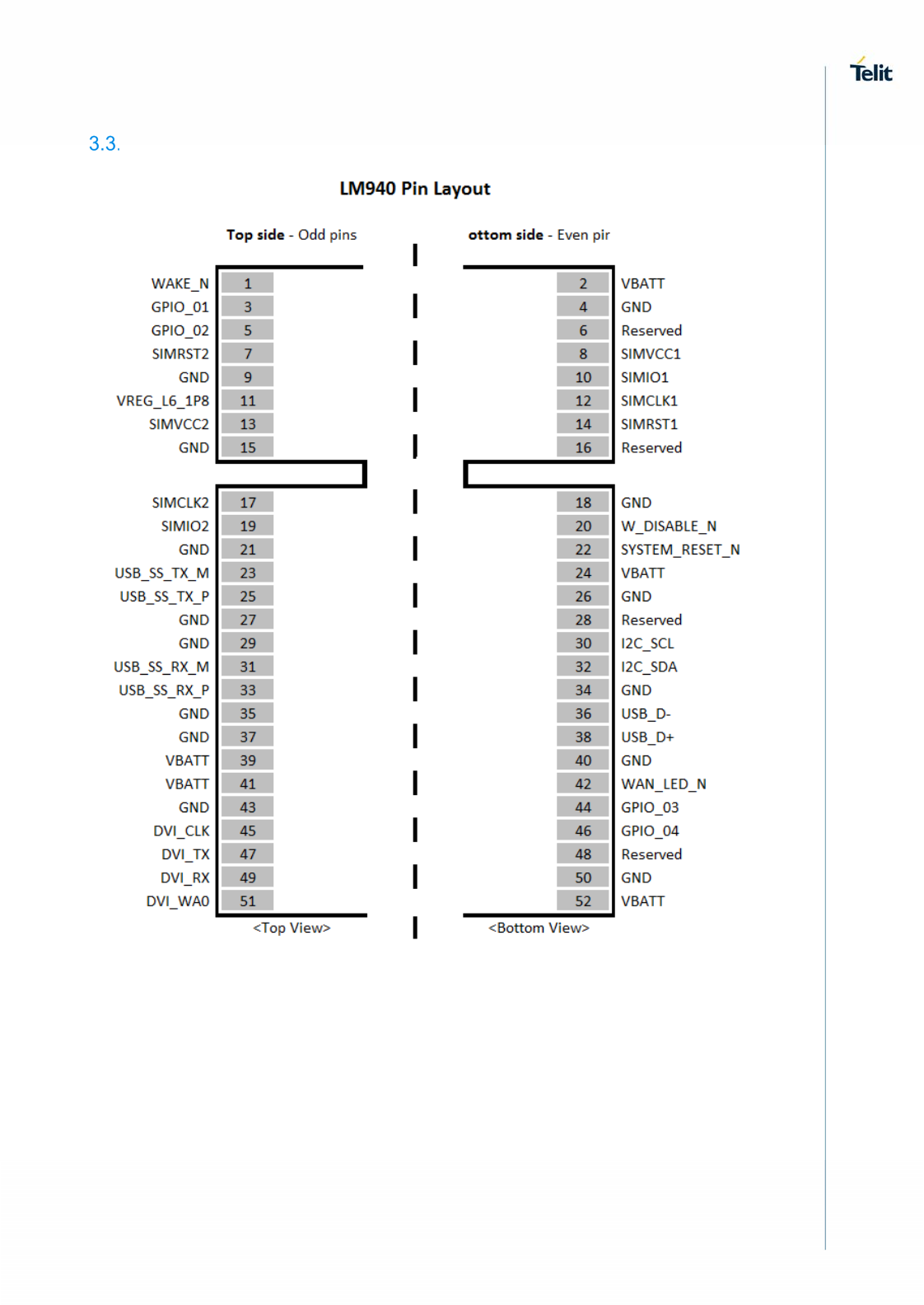
Pin Layout
LM940 HW Design Guide
1VV0301352 Rev. 2 Page 26 of 68 2017-07-19
4. POWER SUPPLY
The power supply circuitry and board layout are very important parts of the full product
design, with critical impact on the overall product performance. Read the following
requirements and guidelines carefully to ensure a good and proper design.
Power Supply Requirements
The LM940 power requirements are as follows:
Power Supply Requirements
Nominal supply voltage 3.3V
Supply voltage range 3.10V – 3.6V
Maximum ripple on module input supply 30 mV
Power Consumption
Below table provides typical current consumption values of LM940 for various operation
modes.
LM940 Current Consumption
Mode Average [Typ.] Mode Description
IDLE Mode
IDLE Mode 60.0 mA No call connection
USB3.0 is connected to a host
Operative Mode (LTE)
LTE (22 dBm) 750 mA LTE data call (Non-CA BW 5MHz, RB=1)
1250 mA
LTE data call (CA_3A+7A+20A,
20MHz+20MHz+20MHz, Full RB, 256QAM
DL / 64QAM UL, FDD 600Mbps DL /
75Mbps UL)
Operative Mode (WCDMA)
WCDMA Voice 650 mA WCDMA voice call (Tx = 23 dBm)
WCDMA HSPA
(22 dBm) 650 mA WCDMA data call (DC-HSDPA up to 42
Mbps, Max Throughput)
* Worst/best case current values depend on network configuration - not under module
control.
** Applied MPR –2dB 16-QAM full RB
*** 3.3 voltage / room temperature
LM940 HW Design Guide
1VV0301352 Rev. 2 Page 27 of 68 2017-07-19
Information – The electrical design for the power supply must ensure
a peak current output of at least 2A.
General Design Rules
The principal guidelines for the Power Supply Design embrace three different design
steps:
Electrical design
Thermal design
PCB layout
4.3.1. Electrical Design Guidelines
The electrical design of the power supply depends strongly on the power source where
this power is drained.
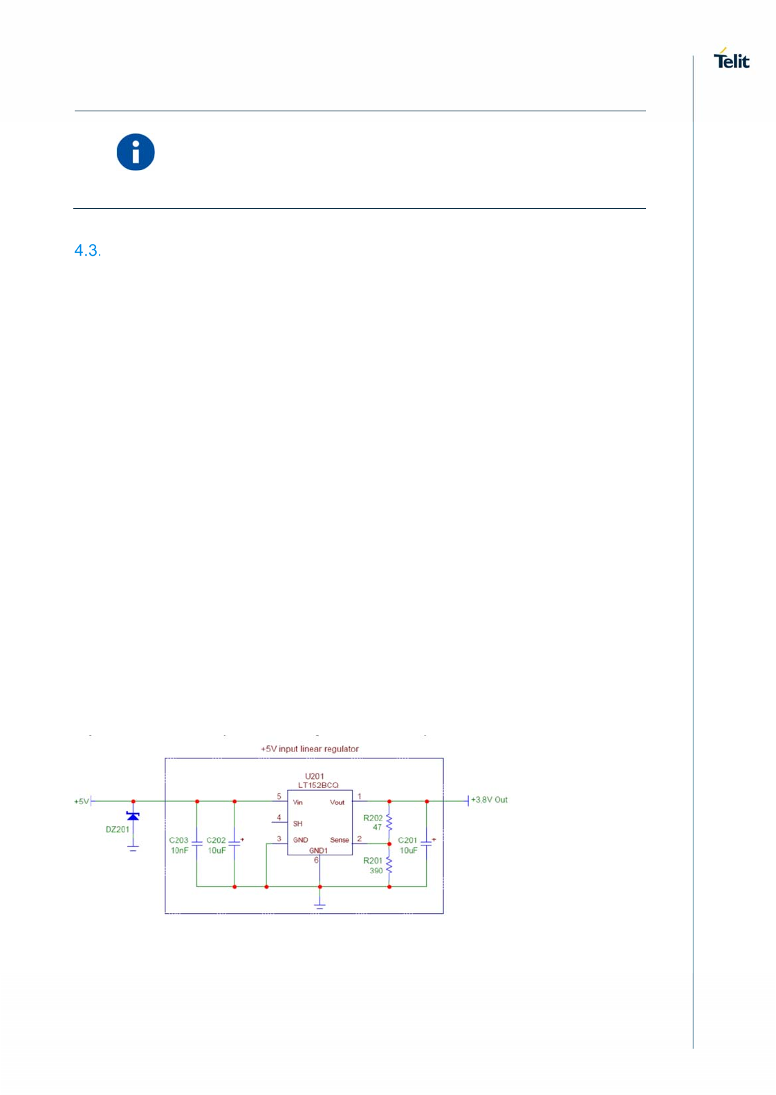
4.3.1.1. + 5V Input Source Power Supply – Design Guidelines
The desired output for the power supply is 3.8V. So, the difference between the
input source and the desired output is not big, and therefore a linear regulator can
be used. A switching power supply is preferred to reduce power consumption.
When using a linear regulator, a proper heat sink must be provided to dissipate the
power generated.
A bypass low ESR capacitor of adequate capacity must be provided to cut the
current absorption peaks close to the LE925A4 module. A 100 μF tantalum
capacitor is usually suitable (on both VPH_PWR and VPH_PWR_RF together).
Make sure that the low ESR capacitor on the power supply output (usually a
tantalum one) is rated at least 10V.
A protection diode must be inserted close to the power input to protect the
LE925A4 module from power polarity inversion.
Figure shows an example of linear regulator with 5V input.
4.3.2. Thermal Design Guidelines
The thermal design for the power supply heat sink must be done with the following
specifications:

LM940 HW Design Guide
1VV0301352 Rev. 2 Page 28 of 68 2017-07-19
Average current consumption during RF transmission @PWR level max in LM940
as shown in Section 4.2, Power Consumption table.
Information – The average consumption during transmission depends
on the power level at which the device is requested to transmit via the
network.
Therefore, the average current consumption varies significantly.
Information – The thermal design for the power supply must be made
keeping an average consumption at the maximum transmitting level
during calls of LTE/HSPA.
Considering the very low current during Idle, especially if the Power Saving function is
enabled, it is possible to consider from the thermal point of view that the device absorbs
significant current only during Data session.
In LTE/WCDMA/HSPA mode, the LM940 emits RF signals continuously during
transmission. Therefore, you must pay special attention how to dissipate the heat
generated.
While designing the application board, the designer must make sure that the LM940
module is located on a large ground area of the application board for effective heat
dissipation.
Information – The LM940 must be connected to the ground and metal
chassis of the host board for best RF performance and thermal
dispersion as well as to have module fixed.
The two holes at the top of the module and the main ground
of the host board must be fastened together.
The shield cover of the module and the main board of the host
board or the metal chassis of the host device should be
connected with conductive materials.
4.3.3. Power Supply PCB layout Guidelines
As seen in the electrical design guidelines, the power supply must have a low ESR
capacitor on the output to cut the current peaks and a protection diode on the input to
protect the supply from spikes and polarity inversion. The placement of these components

LM940 HW Design Guide
1VV0301352 Rev. 2 Page 29 of 68 2017-07-19
is crucial for the correct operation of the circuitry. A misplaced component can be useless
or can even decrease the power supply performances.
The bypass low ESR capacitor must be placed close to the LM940 power input
pins, or if the power supply is of a switching type, it can be placed close to the
inductor to cut the ripple, as long as the PCB trace from the capacitor to LM940 is
wide enough to ensure a drop-less connection even during the 2A current peaks.
The protection diode must be placed close to the input connector where the power
source is drained.
The PCB traces from the input connector to the power regulator IC must be wide
enough to ensure that no voltage drops occur during the 2A current peaks.
The PCB traces to LM940 and the bypass capacitor must be wide enough to
ensure that no significant voltage drops occur when the 2A current peaks are
absorbed. This is needed for the same above-mentioned reasons. Try to keep
these traces as short as possible.
The PCB traces connecting the switching output to the inductor and the switching
diode must be kept as short as possible by placing the inductor and the diode very
close to the power switching IC (only for the switching power supply). This is done
to reduce the radiated field (noise) at the switching frequency (usually 100-
500 kHz).
Use a good common ground plane.
Place the power supply on the board in a way to guarantee that the high current
return paths in the ground plane do not overlap any noise sensitive circuitry, such
as the microphone amplifier/buffer or earphone amplifier.
The power supply input cables must be kept separate from noise sensitive lines,
such as microphone/earphone cables.
RTC
The RTC within the LM940 module does not have a dedicated RTC supply pin. The RTC
block is supplied by the VBATT supply.
If VBATT power is removed, RTC is not maintained so if maintaining an internal RTC is
needed, VBATT must be supplied continuously.
Reference Voltage
1.8V regulated power supply output is provided as the reference voltage to a host board.
This output is active when the module is ON and goes OFF when the module is shut
down.
This table lists the VREG_L6_IP8 signal of LM940.
LM940 Reference Voltage
PIN Signal I/O Function Type Comment
11 VREG_L6_1P8 O Reference Voltage power 1.8V

LM940 HW Design Guide
1VV0301352 Rev. 2 Page 30 of 68 2017-07-19
Internal LDO for GNSS bias
The LDO for GNSS bias is applied inside the LM940 model.
The voltage supply come from LM940’s LDO to GNSS active antenna.
This table lists the LDO for GNSS bias of LM940.
LM940 Reference Voltage
Symbol Parameter Min Typ Max Unit
V
GNSS DC bias
Voltage of Internal LDO for GNSS bias 2.9 3.1 3.3 [V]
I
GNSS DC bias
Current of Internal LDO for GNSS bias - - 50 [mA]
LM940 HW Design Guide
1VV0301352 Rev. 2 Page 31 of 68 2017-07-19
5. ELECTRICAL SPECIFICATIONS
Absolute Maximum Ratings – Not Operational
Caution – A deviation from the value ranges listed below may
harm the LM940 module.
Absolute Maximum Ratings – Not Operational
Symbol Parameter Min Max Unit
VBATT Battery supply voltage on pin VBATT -0.5 +4.0 [V]
Recommended Operating Conditions
Recommended Operating Conditions
Symbol Parameter Min Typ Max Unit
T
amb
Ambient temperature -40 +25 +85 [°C]
VBATT Battery supply voltage on pin VBATT 3.1 3.3 3.6 [V]
I
VBATT +
I
VBATT_PA
Peak current to be used to dimension
decoupling capacitors on pin VBATT - 80 2500 [mA]
LM940 HW Design Guide
1VV0301352 Rev. 2 Page 32 of 68 2017-07-19
6. DIGITAL SECTION
Logic Levels
Unless otherwise specified, all the interface circuits of the LM940 are 1.8V CMOS logic.
Only USIM interfaces are capable of dual voltage I/O.
The following tables show the logic level specifications used in the LM940 interface
circuits. The data specified in the tables below is valid throughout all drive strengths and
the entire temperature ranges.
Caution – Do not connect LM940’s digital logic signal directly to
OEM’s digital logic signal with a level higher than 2.3V for 1.8V
CMOS signals.
6.1.1. 1.8V Pins – Absolute Maximum Ratings
Absolute Maximum Ratings – Not Functional
Parameter Min Max
Input level on any digital pin when on -- +2.16V
Input voltage on analog pins when on -- +2.16 V
6.1.2. 1.8V Standard GPIOs
Operating Range – Interface Levels (1.8V CMOS)
Parameter Min Max Unit Comment
VIH Input high level 1.17V 2.1V [V]
VIL Input low level -0.3V 0.63V [V]
VOH Output high level 1.35V 1.8V [V]
VOL Output low level 0V 0.45V [V]
IIL Low-level input leakage
current
-1 -- [uA] No pull-up
IIH High-level input leakage
current
-- 1 [uA] No pull-down
IILPU Low-level input leakage
current
-97.5 -27.5 [uA] With pull-up
LM940 HW Design Guide
1VV0301352 Rev. 2 Page 33 of 68 2017-07-19
Parameter Min Max Unit Comment
IIHPD High-level input leakage
current
27.5 97.5 [uA] With pull-down
CI/o I/O capacitance -- 5 [pF]
6.1.3. 1.8V SIM Card Pins
Operating Range – SIM Pins Working at 1.8V
Parameter Min Max Unit Comment
VIH Input high level 1.26V 2.1V [V]
VIL Input low level -0.3V 0.36V [V]
VOH Output high level 1.44V 1.8V [V]
VOL Output low level 0V 0.4V [V]
IIL Low-level input leakage
current
-- 1000 [uA] No pull-up
IIH High-level input leakage
current
-20 20 [uA] No pull-down
6.1.4. 2.85V Pins – Absolute Maximum Ratings
Absolute Maximum Ratings – Not Functional
Parameter Min Max
Input level on any digital pin when on -- +3.42V
Input voltage on analog pins when on -- +3.42 V
6.1.5. SIM Card Pins @2.85V
Operating Range – For SIM Pins Operating at 2.85V
Parameter Min Max Unit Comment
VIH Input high level 1.995V 3.15V [V]
VIL Input low level -0.3V 0.57V [V]
VOH Output high level 2.28V 2.85V [V]
VOL Output low level 0V 0.4V [V]
LM940 HW Design Guide
1VV0301352 Rev. 2 Page 34 of 68 2017-07-19
Parameter Min Max Unit Comment
IIL Low-level input leakage
current
-- 1000 [uA] No pull-up
IIH High-level input leakage
current
-20 20 [uA] No pull-down
Power On
The LM940 is automatically turning on when the VBATT is supplied.
Information – To turn on the LM940 module, the W_DISABLE_N pin
must not be asserted low.
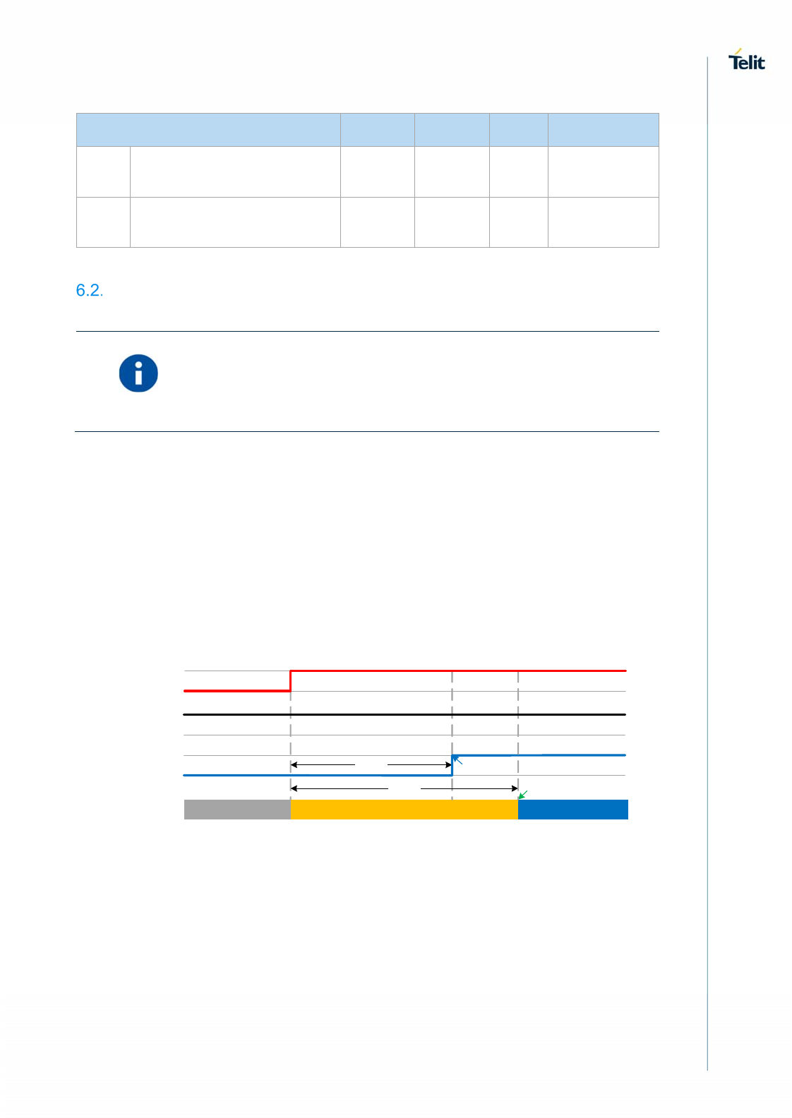
6.2.1. Initialization and Activation State
After turning on the LM940 module, the LM940 is not yet activated because the SW
initialization process of the LM940 module is still in process internally. It takes some time
to fully complete the HW and SW initialization of the module.
For this reason, it is impossible to access LM940 during the Initialization state.
As shown in below figure, the LM940 becomes operational (in the Activation state) at least
15 seconds after the VBATT is supplied.
LM940 Initialization and Activation
InitializationState ActivationState
InternalState
VREG_L6_1P8
W_DISABLE_N
OFFState
TBDsec
USBDriverLoaded
AllInterfacesAndPinsConfigured
VBATT
TBDsec

LM940 HW Design Guide
1VV0301352 Rev. 2 Page 35 of 68 2017-07-19
Information – To check if the LM940 has completely powered on,
LM940 and the host must be connected via USB. When USB driver
completely loaded, the module has completely powered on and is
ready to accept AT commands.
Information – During SW initialization of the LM940, the SW configures
all pins and interfaces to their desired mode. When VREG_L6_1P8
goes high, this indicates that the initialization of all I/O pins is
completed.
Information – Active low signals are labeled with a name that ends with
“_N”
Information – To avoid a back-powering effect, it is recommended to
avoid having any HIGH logic level signal applied to the digital pins of
the module when it is powered OFF or during an ON/OFF transition.
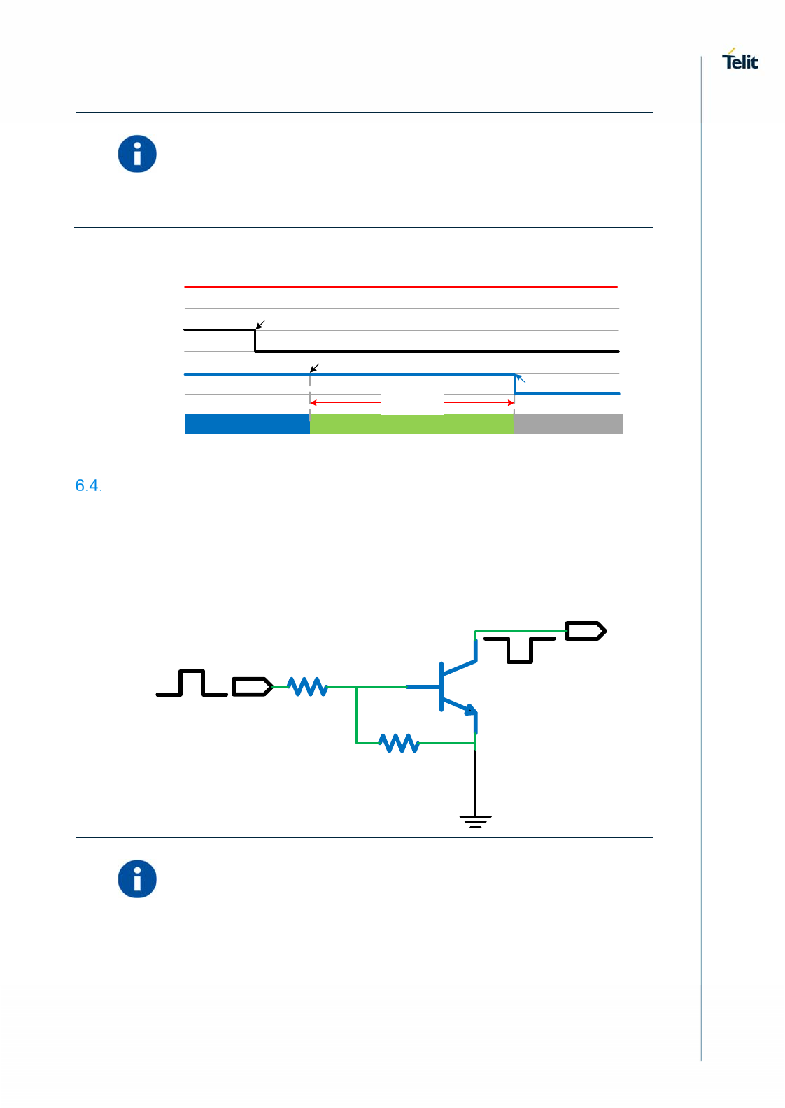
Power Off
The LM940 module can be shut down by a software command.
When a shutdown command is sent, LM940 goes into the Finalization state and at the end
of the finalization process shuts down VREG_L6_1P8. The duration of the finalization
state can differ according to the current situation of the module, so a value cannot be
defined.
Usually, it will take more than 12 seconds from sending a shutdown command until
reaching a complete shutdown. The DTE should monitor the status of VREG_L6_1P8 to
observe the actual power-off.
Information – To completely shut down the LM940 module, the
W_DISABLE_N pin must be asserted low.
Otherwise, the LM940 will turn on again after shut down.
LM940 HW Design Guide
1VV0301352 Rev. 2 Page 36 of 68 2017-07-19
Information – To avoid a back-powering effect, it is recommended to
avoid having any HIGH logic level signal applied to the digital pins of
the module when it is powered OFF or during an ON/OFF transition.
Shutdown by Software Commnad
FinalizationState OFFState
InternalState
VREG_L6_1P8
VPH_PWR
ActivationState
AT#SHDN
VariableAbove
TBDsec
MonitoringStatus
W_DISABLE_N
MustBeAssertedLow.
Unconditional Hardware Reset
To unconditionally restart the LM940 module, the SYSTEM_RESET_N pin must be
asserted low for a between 100 milliseconds and 150milliseconds then released.
Below figure shows a simple circuit for this action.
Circuit for Unconditional Hardware Reset
GND
R1
R2
Q1
Unconditional
ResetImpulse
100 ms<HoldTime<150ms
SYSTEM_RESET_N
Information – The Unconditional Hardware Reset must be used only
as an emergency exit procedure, and not as a normal power-off
operation.
LM940 HW Design Guide
1VV0301352 Rev. 2 Page 37 of 68 2017-07-19
Information – Do not use any pull-up resistor on the RESET_N line or
any totem pole digital output. Using a pull-up resistor may cause latch-
up problems on the LM940 power regulator and improper functioning
of the module. The RESET_N line must be connected only in an open-
collector configuration.
Communication ports
Below table summarizes all the hardware interfaces of the LM940 module.
LM940 Hardware Interfaces
6.5.1. USB Interface
The LM940 module includes super-speed USB3.0 with high-speed USB2.0 backward
compatibility. It is compliant with Universal Serial Bus Specification, Revision 3.0 and can
be used for control and data transfers as well as for diagnostic monitoring and firmware
update.
The USB port is typically the main interface between the LM940 module and OEM
hardware.
USB 3.0 needs series capacitors on the TX lines in both directions for AC coupling. In
order to interface USB3.0 with an application board of customer, 0.1uF capacitors should
be installed on USB_SS_RX_P/M lines of the LM940. There are already series capacitors
on USB_SS_TX_P/M lines inside LM940 module.
The USB interface suggested connection is the following:
Connection for USB Interface
Interface LM940
USB Super-speed USB3.0 with high-speed USB2.0
USIM x2, dual voltage each (1.8V/2.85V)
Control Signals W_DISABLE_N, WAKE_N, WAN_LED_N
GPIO X4, GPIO
I2C I2C (optional)
Audio I/F PCM (optional)
Antenna ports 2 for Cellular, 1 for GNSS
LM940 HW Design Guide
1VV0301352 Rev. 2 Page 38 of 68 2017-07-19
Information – The USB signal traces must be routed carefully.
Minimize trace lengths, number of vias, and capacitive loading. The
impedance value should be as close as possible to 90 Ohms
differential.
Below table lists the USB interface signals.
USB Interface Signals
PIN Signal I/O Function Type Comment
38 USB_D+ I/O USB 2.0 Data Plus Analog
36 USB_D- I/O USB 2.0 Data Minus Analog
33 USB_SS_RX_P I USB 3.0 super-speed
receive – plus Analog
31 USB_SS_RX_M I USB 3.0 super-speed
receive – minus Analog
25 USB_SS_TX_P O USB 3.0 super-speed
transmit – plus Analog
23 USB_SS_TX_M O USB 3.0 super-speed
transmit – minus Analog
Information – Even if USB communication is not used, it is still highly
recommended to place an optional USB connector on the application
board.
At least test points of the USB signals are required since the USB
physical communication is needed in the case of SW update.
LM940 HW Design Guide
1VV0301352 Rev. 2 Page 39 of 68 2017-07-19
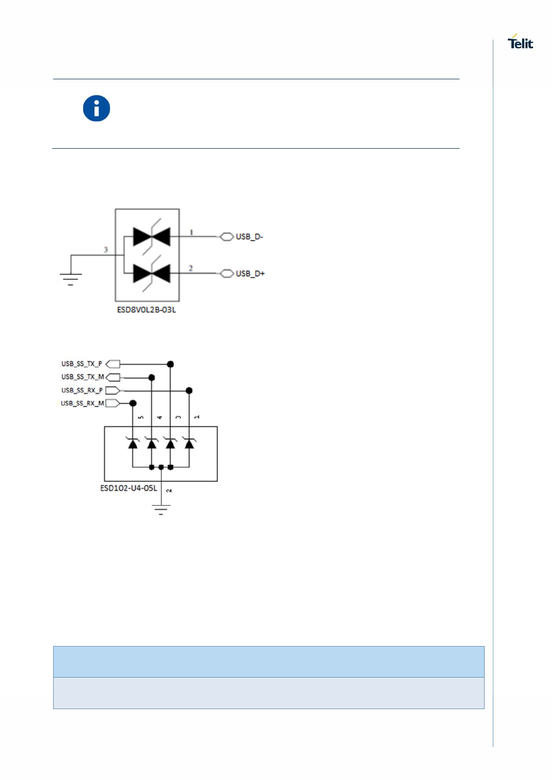
Information – Consider placing a low-capacitance ESD protection
component to protect LM940 against ESD strikes
If an ESD protection should be added, the suggested connectivity is as follows:
ESD Protection for USB2.0
ESD Protection for USB3.0
6.5.2. SIM Interface
The LM940 supports two external SIM interfaces (1.8V or 2.85V).
Below table lists the SIM interface signals.
SIM Interface Signals
PIN Signal I/O Function Type Comment
SIM Card Interface 1
LM940 HW Design Guide
1VV0301352 Rev. 2 Page 40 of 68 2017-07-19
6.5.2.1. SIM Schematic Example
The following Figures illustrate in particular how the application side should be designed.
SIM Schematics
SIM_CARD
LM940
SIMIO
SIMCLK
SIMRST
SIMVCC C1
C2
C3
C5
C6
C7
1
2
3
4
5
6
78
C1
C2
C3
C4
...
33pF
(DNI)
33pF
(DNI)
33pF
(DNI)
100nF
.
SIMIN
8 SIMVCC1 O Supply output for an
external UIM1 card
1.8V / 2.85V Power
10 SIMIO1 I/O Data connection with an
external UIM1 card
1.8V / 2.85V
12 SIMCLK1 O Clock output to an
external UIM1 card
1.8V / 2.85V
14 SIMRST1 O Reset output to an
external UIM1 card
1.8V / 2.85V
SIM Card Interface 2
13 SIMVCC2 O Supply output for an
external UIM2 card
1.8 / 2.85V Power
19 SIMIO2 I/O Data connection with an
external UIM2 card
1.8 / 2.85V
17 SIMCLK2 O Clock output to an
external UIM2 card
1.8 / 2.85V
7 SIMRST2 O Reset output to an
external UIM2 card
1.8 / 2.85V
Digital I/O (GPIOs)
3 GPIO_01 I UIM1 Card Present
Detect
1.8V GPIO_01 can be
used as SIMIN1
5 GPIO_02 I UIM2 Card Present
Detect
1.8V GPIO_02 can be
used as SIMIN2
LM940 HW Design Guide
1VV0301352 Rev. 2 Page 41 of 68 2017-07-19
Information – LM940 contains an internal pull-up resistor on SIMIO. It
is not necessary to install external pull – up resistor.
6.5.3. Control Signals
The LM940 supports the following control signals:
W_DISABLE_N
WAKE_N
WAN_LED_N
Below table lists the control signals of LM940.
Module Control Signal
PIN Signal I/O Function Type Comment
20 W_DISABLE_N I RF disable (airplane mode) 1.8V
1 WAKE_N O Host wake-up 1.8V
42 WAN_LED_N O LED control 1.8V
6.5.3.1. W_DISABLE_N
The W_DISABLE_N signal is provided to make the LM940 goes into the airplane mode:
Enter into the airplane mode: Low
Normal operating mode: High or Leave the W_DISABLE_N not connected
The W_DISABLE_N should be controlled when the LM940 to either turn on or off.
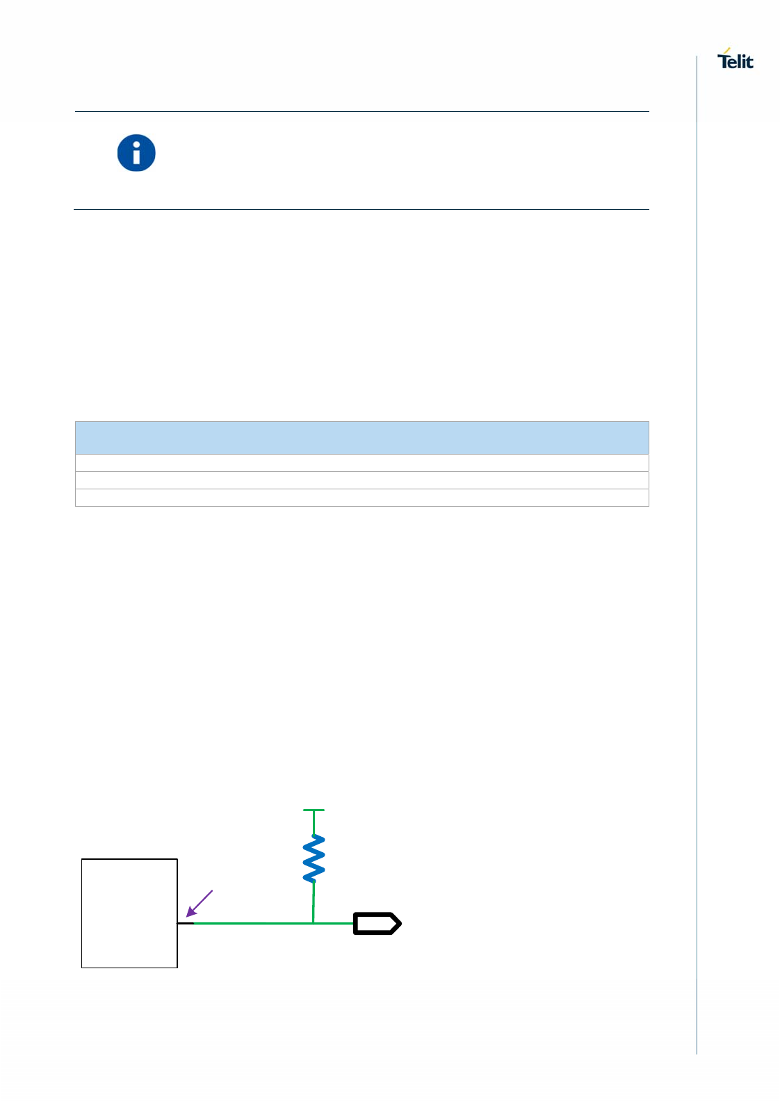
6.5.3.2. WAKE_N
The WAKE_N signal wakes the host when specific events occur.
Recommended WAKE_N connection is the following:
Recommended WAKE_N connection
LM940
WAKE_N
Opencollector
HostInput
R1
VCC
LM940 HW Design Guide
1VV0301352 Rev. 2 Page 42 of 68 2017-07-19
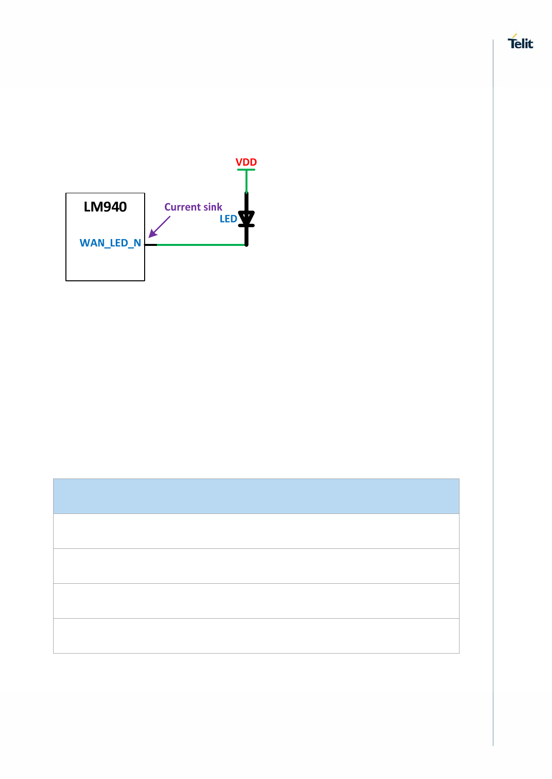
6.5.3.3. WAN_LED_N
The WAN_LED_N signal drives the LED output.
The recommended WAN_LED_N connection is the following:
Recommended WAN_LED_N connection
6.5.4. General Purpose I/O
The general-purpose I/O pins can be configured to act in three different ways:
Input
Output
Dedicate Function (Customer Requirement)
Input pins can only be read and report digital values (high or low) present on the pin at the
read time. Output pins can only be written or queried and set the value of the pin output.
The following GPIOs are always available as a primary function on the LM940.
Below table lists the GPIO signals of LM940.
GPIOs
Pin no. Signal I/O Function Type Drive
Strength
3 GPIO_01 I/O Configurable
GPIO
CMOS
1.8V
2-16 mA
5 GPIO_02 I/O Configurable
GPIO
CMOS
1.8V
2-16 mA
44 GPIO_03 I/O Configurable
GPIO
CMOS
1.8V
2-16 mA
46 GPIO_04 I/O Configurable
GPIO
CMOS
1.8V
2-16 mA
LM940 HW Design Guide
1VV0301352 Rev. 2 Page 43 of 68 2017-07-19
6.5.4.1. Using a GPIO Pin as Input
GPIO pins, when used as inputs, can be tied to a digital output of another device and
report its status, provided the device interface levels are compatible with the GPIO 1.8V
CMOS levels.
If a digital output of a device is tied to GPIO input, the pin has interface levels different
than 1.8V CMOS. It can be buffered with an open collector transistor with a 47 kΩ pull-up
resistor to 1.8V.
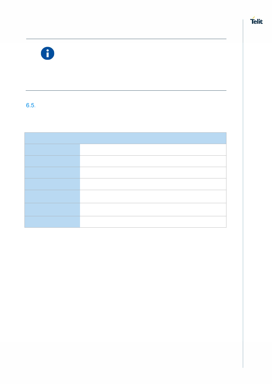
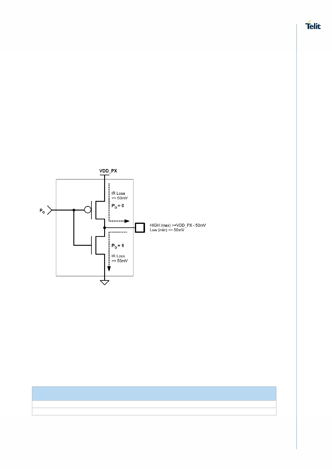
6.5.4.2. Using a GPIO Pin as Output
GPIO pins, when used as outputs, can drive 1.8V CMOS digital devices or compatible
hardware. When set as outputs, the pins have a push-pull output, and therefore the pull-
up resistor can be omitted.
GPIO Output Pin Equivalent Circuit
6.5.5. I2C – Inter-integrated circuit
The LM940 supports an I2C interface on the following pins:
Below table lists the I2C signals of LM940.
Module I2C Signal
PIN Signal I/O Function Type Comment
30 I2C_SCL O I2C Clock CMOS 1.8V
32 I2C_SDA I/O I2C Data CMOS 1.8V
The I2C interface is used for controlling peripherals inside the module (such as codec,
etc.).

LM940 HW Design Guide
1VV0301352 Rev. 2 Page 44 of 68 2017-07-19
Information – I2C is supported only on from Modem side as SW
emulation of I2C on GPIO lines.
Please contact us if you use it.
Information – If the I2C interface is not used, the signals can be left
floating.
Using the Temperature Monitor Function
The Temperature Monitor permits to monitor the module’s internal temperature and, if
properly set (see the #TEMPSENS command in LM940 AT Commands Reference Guide
), raises a GPIO to High Logic level when the maximum temperature is reached.

LM940 HW Design Guide
1VV0301352 Rev. 2 Page 45 of 68 2017-07-19
7. RF SECTION
Antenna requirements
The antenna connection is one of the most important aspect in the full product design as it
strongly affects the product overall performance. Hence read carefully and follow the
requirements and the guidelines for a proper design.
The LM940 is provided with three RF connectors.
The available connectors are:
Main RF antenna: TX/RX path
Auxiliary RF antenna: Combined Diversity and GNSS
GNSS RF antenna: Dedicated GNSS
Main Antenna Requirements
The antenna for the LM940 device must meet the following requirements:
WCDMA / LTE Antenna Requirements
Frequency range Depending by frequency band(s) provided by the network
operator, the customer shall use the most suitable antenna for
that/those band(s)
The bands supported by the LM940 is provided in Section 2.2,
Product Variants and Frequency Bands.
Impedance 50 Ohm
Input power > 24 dBm average power in WCDMA & LTE
VSWR absolute max <= 10:1
VSWR recommended <= 2:1
Antenna Diversity Requirements
This product includes an input for a second Rx antenna to improve radio sensitivity. The
function is called Antenna Diversity.
Antenna Diversity Requirements
Frequency range Depending by frequency band(s) provided by the network
operator, the customer shall use the most suitable antenna for
that/those band(s)
The bands supported by the LM940 is provided in Section 2.2,
Product Variants and Frequency Bands.
Impedance 50Ω
VSWR recommended ≤ 2:1

LM940 HW Design Guide
1VV0301352 Rev. 2 Page 46 of 68 2017-07-19
The second Rx antenna should not be located in the close vicinity of main antenna. In
order to improve Diversity Gain, Isolation and reduce mutual interaction, the two antennas
should be located at the maximum reciprocal distance possible, taking into consideration
the available space into the application. For the same reason, the Rx antenna should also
be cross-polarized with respect to the main antenna.
Isolation between main antenna and Rx antenna must be at least 10 dB in all uplink
frequency bands.
Envelope Correlation Coefficient (ECC) value should be as close as possible to zero, for
best diversity performance. ECC values below 0.5 on all frequency bands are
recommended.
GNSS Receiver
The LM940 integrates a GNSS receiver that could be used in Standalone mode and in A-
GPS (assisted GPS), according to the different configurations.
LM940 supports an active antenna.
Frequency range • Wide-band GNSS:
1560–1606 MHz recommended
• Narrow-band GPS:
1575.42 MHz ± 2 MHz minimum
• Narrow-band Galileo:
1575.42 MHz ± 2 MHz minimum
• Narrow-band BeiDou:
1561.098 MHz ± 2 MHz minimum
• Narrow-band GLONASS:
1601.72 MHz ± 4.2 MHz minimum.
Gain 1.5 dBi < Gain < 3 dBi
Impedance 50 Ohm
Amplification 18 dB < Gain < 21 dB
Supply Voltage 3.1 V
Current consumption 20 mA Typical
7.4.1. GNSS RF Front End Design
The LM940 contains an integrated LNA and pre-select SAW filter.
This allows the module to work well with a passive GNSS antenna. If the antenna cannot
be located near the LM940, then an active antenna (that is, an antenna with a low noise
amplifier built in) can be used with an external dedicated power supply circuit.
GNSS rescive path uses either the dedicated GNSS connector or the shared AUX
connector.
LM940 HW Design Guide
1VV0301352 Rev. 2 Page 47 of 68 2017-07-19
NOTE – Please refer to the LM940 AT Commands Reference Guide,
80545ST10791A for detailed information about GNSS operating
modes and GNSS Antenna selection.
Antenna connection
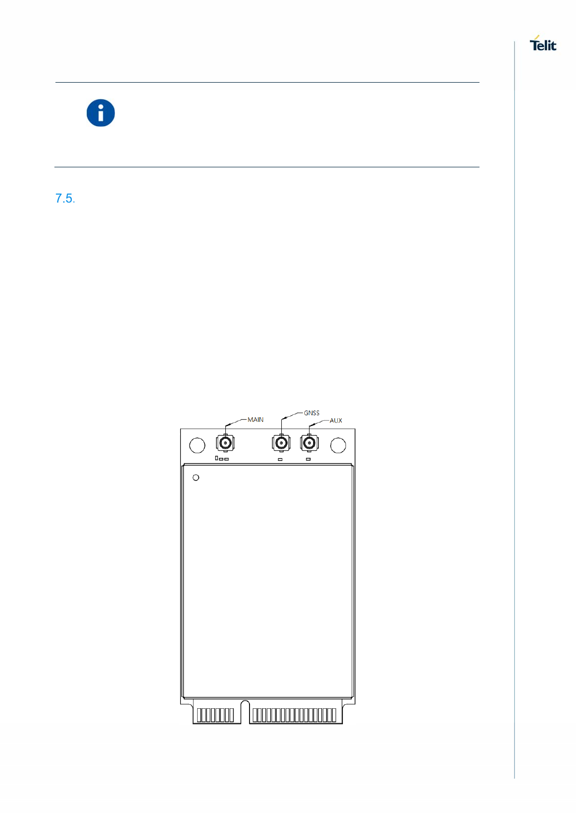
7.5.1. Antenna Connector
The LM940 is equipped with a set of 50 Ω RF U.FL. connectors from Hirose U.FL-R-SMT-
1(10).
The available connectors are:
Main RF antenna: TX/RX path
Auxiliary RF antenna: Combined Diversity and GNSS
GNSS RF antenna: Dedicated GNSS
See the picture on the below for their position on the interface.
LM940 HW Design Guide
1VV0301352 Rev. 2 Page 48 of 68 2017-07-19
For more information about mating connectors visit the website http://www.hirose-
connectors.com/
7.5.2. Antenna Cable
Connecting cables between the module and the antenna must have 50 Ω impedance.
If the impedance of the module is mismatched, RF performance is reduced significantly.
If the host device is not designed to use the module’s diversity or GNSS antenna,
terminate the interface with a 50Ω load.
Minimize Antenna Cable Requirements
Impedance 50 Ohm
Max cable loss 0.5 dB
Avoid coupling with other signals.
7.5.3. Antenna Installation Guidelines
Install the antenna in a location with access to the network radio signal.
The antenna must be installed such that it provides a separation distance of at
least 20 cm from all persons and must not be co-located or operating in
conjunction with any other antenna or transmitter.
The antenna must not be installed inside metal cases.
The antenna must be installed according to the antenna manufacturer’s
instructions.
Furthermore, if the device is developed for the US and/or Canada market, it must comply
with the FCC and/or IC approval requirements.
Information
This device is to be used only for mobile and fixed application. The
antenna(s) used for this transmitter must be installed to provide a
separation distance of at least 20 cm from all persons and must not be
co-located or operating in conjunction with any other antenna or
transmitter. End-Users must be provided with transmitter operation
conditions for satisfying RF exposure compliance. OEM integrators
must ensure that the end user has no manual instructions to remove
or install the LM940 module. Antennas used for this OEM module must
not exceed gain of below table for mobile and fixed operating
configurations.
In the event that these conditions cannot be met (for example certain
laptop configurations or co-location with another transmitter), then the
FCC/IC authorization is no longer considered valid and the FCC/IC ID
cannot be used on the final product. In these circumstances, the OEM
integrator will be responsible for re-evaluating the end product
(including the transmitter) and obtaining a separate FCC/IC
authorization.

LM940 HW Design Guide
1VV0301352 Rev. 2 Page 49 of 68 2017-07-19
Manual Information to the End User
The OEM integrator has to be aware not to provide information to the
end user regarding how to install or remove this RF module in the
user’s manual of the end product which integrates this module. The
end user manual shall include all required regulatory
information/warning as show in this manual.
LM940 HW Design Guide
1VV0301352 Rev. 2 Page 50 of 68 2017-07-19
8. AUDIO SECTION
Audio Interface
The LM940 module supports digital audio interfaces.
Digital Audio
The LM940 module can be connected to an external codec through the digital interface.
The product provides a single Digital Audio Interface on the following pins:
Digital Audio Interface Signals
Pin no. Signal I/O Function Type COMMENT
51 DVI_WAO O PCM Frame
Sync B-PD 1.8V
49 DVI_RX I PCM Data In B-PD 1.8V
47 DVI _TX O PCM Data Out B-PD 1.8V
45 DVI _CLK O PCM Clock B-PD 1.8V
LM940 PCM has the following characteristics:
PCM Master mode using short or long frame sync modes
16 bit linear PCM format
PCM clock rates of 256 kHz, 512 kHz, 1024 kHz and 2048 kHz (Default)
Frame size of 8, 16, 32, 64, 128 & 256 bits per frame
Sample rates of 8 kHz and 16 kHz
NOTE – If the Digital Audio Interface is not used, the signals can be
left floating.
LM940 HW Design Guide
1VV0301352 Rev. 2 Page 51 of 68 2017-07-19
9. MECHANICAL DESIGN
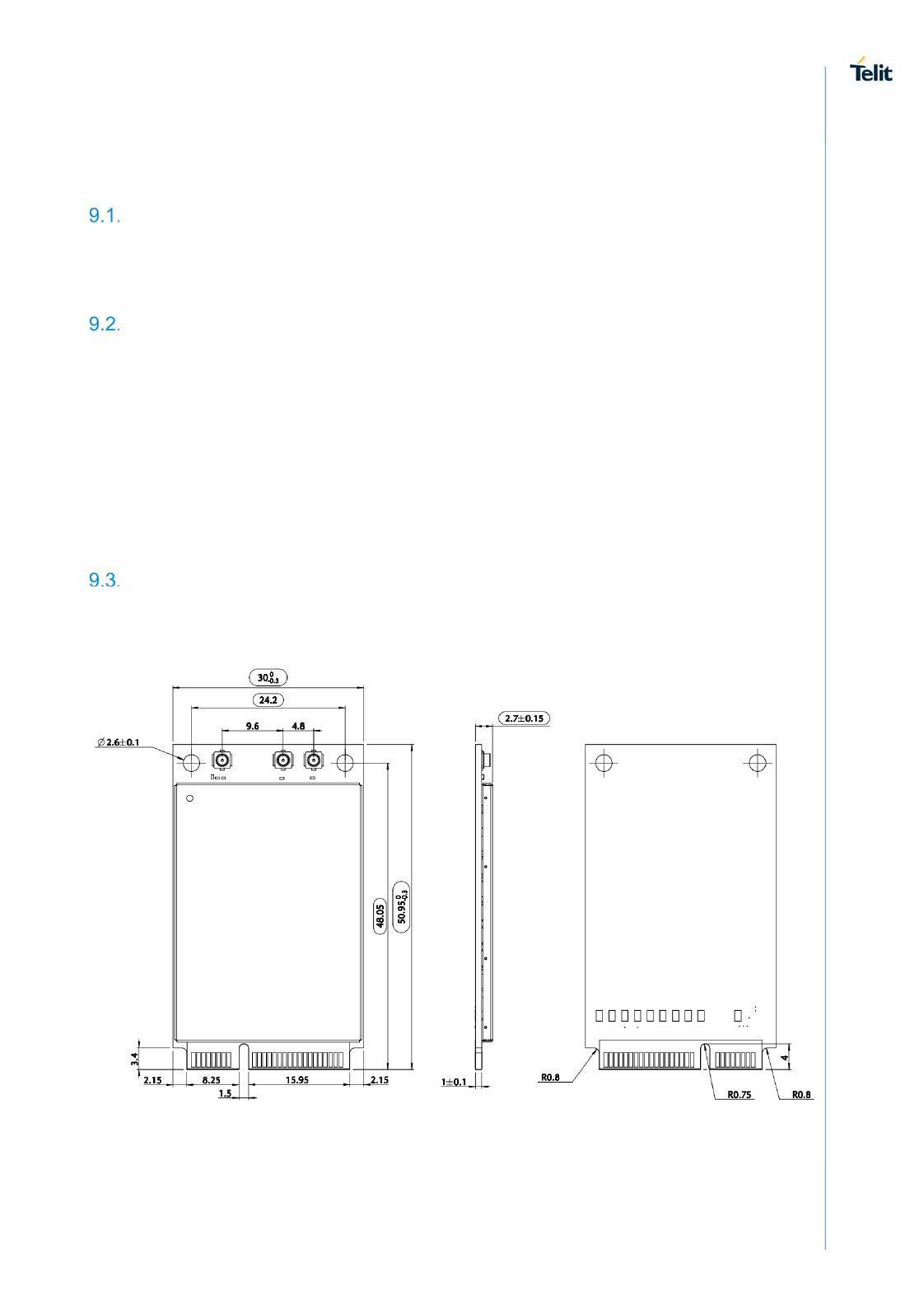
General
The LM940 module was designed to be compliant with a standard lead-free SMT process.
Moreover, it is compatible with the Mini PCIe card 52-pin card edge-type connector.
Finishing & Dimensions
The LM940 module’s overall dimensions are:
Length: 50.95 mm
Width: 30.00 mm
Thickness: 2.70 mm
The module complies with the standard dimensions specified in the PCI Express Mini
Card Electromechanical Specification Revision 1.1
Drawing
This figure shows the mechanical dimensions of the LM940 module.

LM940 HW Design Guide
1VV0301352 Rev. 2 Page 52 of 68 2017-07-19
10. APPLICATION GUIDE
Debug of the LM940 Module in Production
To test and debug the mounting of the LM940 module, we strongly recommend to add
several test pins on the host PCB for the following purposes:
Checking the connection between the LM940 itself and the application
Testing the performance of the module by connecting it with an external computer
Depending on the customer application, these test pins include, but are not limited to the
following signals:
SYSTEM_RESET_N, W_DISABLE_N, WAKE_N
VBATT, GND
VREG_L6_1P8
USB_D-, USB_D+
USB_SS_TX_M, USB_SS_TX_P, USB_SS_RX_M, USB_SS_RX_P
In addition, the following signals are also recommended (but not mandatory):
WAN_LED_N
GPIO_01, GPIO_02, GPIO_03, GPIO_04
Bypass Capacitor on Power Supplies
When a sudden voltage step is asserted to or a cut from the power supplies, the steep
transition causes some reactions such as overshoot and undershoot. This abrupt voltage
transition can affect the device causing it to not operate or to malfunction.
Bypass capacitors are needed to alleviate this behavior. The behavior can appear
differently depending on the various applications. Customers must pay special attention to
this issue when they design their application board.
The length and width of the power lines must be considered carefully, and the capacitance
of the capacitors must be selected accordingly.
The capacitor will also prevent ripple of the power supplies and the switching noise
caused in TDMA systems such as GSM.
Especially, a suitable bypass capacitor must be mounted on the following lines on the
application board:
VBATT
Recommended values are:
100uF for VBATT
Customers must still consider that the capacitance mainly depends on the conditions of
their application board.
Generally, more capacitance is required when the power line is longer.
And if customers use the fast power down function, then more bypass capacitors should be
mounted on the application board.

LM940 HW Design Guide
1VV0301352 Rev. 2 Page 53 of 68 2017-07-19
EMC Recommendations
EMC protection on the pins in the table below should be designed by application side
according to the customer’s requirement.
EMC Recommendations
Pin Signal I/O Function Type Comment
USB HS 2.0 Communication Port
38 USB_D+ I/O USB 2.0 Data Plus Analog
36 USB_D- I/O USB 2.0 Data Minus Analog
USB SS 3.0 Communication Port
33 USB_SS_RX_P I USB 3.0 super-
speed receive – plus
Analog
31 USB_SS_RX_M I USB 3.0 super-
speed receive –
minus
Analog
25 USB_SS_TX_P O USB 3.0 super-
speed transmit –
plus
Analog
23 USB_SS_TX_M O USB 3.0 super-
speed transmit –
minus
Analog
SIM Card Interface 1
14 SIMRST1 O Reset output to an
external UIM1 card
1.8 / 2.85V
12 SIMCLK1 O Clock output to an
external UIM1 card
1.8 / 2.85V
10 SIMIO1 I/O Data connection with
an external UIM1
card
1.8 / 2.85V

LM940 HW Design Guide
1VV0301352 Rev. 2 Page 54 of 68 2017-07-19
8 SIMVCC1 O Supply output for an
external UIM1 card
1.8 / 2.85V Power
SIM Card Interface 2
7 SIMRST2 O Reset output to an
external UIM2 card
1.8 / 2.85V
17 SIMCLK2 O Clock output to an
external UIM2 card
1.8 / 2.85V
19 SIMIO2 I/O Data connection with
an external UIM2
card
1.8 / 2.85V
13 SIMVCC2 O Supply output for an
external UIM2 card
1.8 / 2.85V Power
Digital I/O (GPIOs)
3 GPIO_01 I/O General purpose I/O 1.8V
5 GPIO_02 I/O General purpose I/O 1.8V
44 GPIO_03 I/O General purpose I/O 1.8V
46 GPIO_04 I/O General purpose I/O 1.8V
1 WAKE_N O Host wake-up 1.8V Active Low
42 WAN_LED_N O LED control 1.8V
Power ON/OFF Reset IN/OUT
20 W_DISABLE_N I Module & RF
ON/OFF Control
1.8V Active Low
22 SYSTEM_RESET_N I Reset Input 1.8V Active Low
1.8V Voltage Regulator
11 VREG_L6_1P8 O LDO out for 1.8V Power

LM940 HW Design Guide
1VV0301352 Rev. 2 Page 55 of 68 2017-07-19
All other pins have the following characteristics:
Human Body Model (HBM): ± 1000 V
Charged Device Model (CDM) JESD22-C101-C: ± 250 V
All Antenna pins up to ± 4 kV
Warning – Do not touch without proper electrostatic protective
equipment. The product must be handled with care, avoiding any
contact with the pins because electrostatic discharge may damage the
product itself.
LM940 HW Design Guide
1VV0301352 Rev. 2 Page 56 of 68 2017-07-19
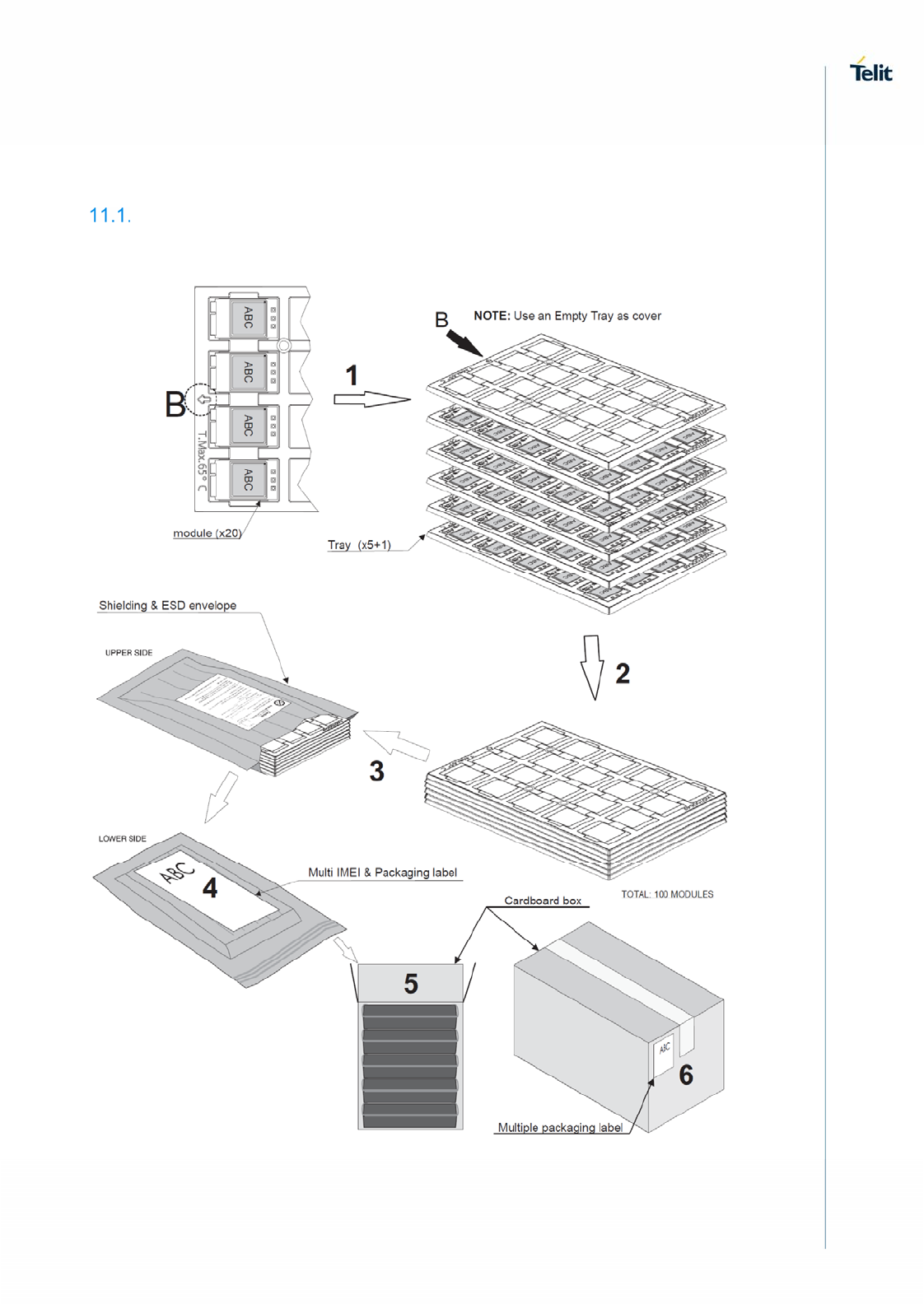
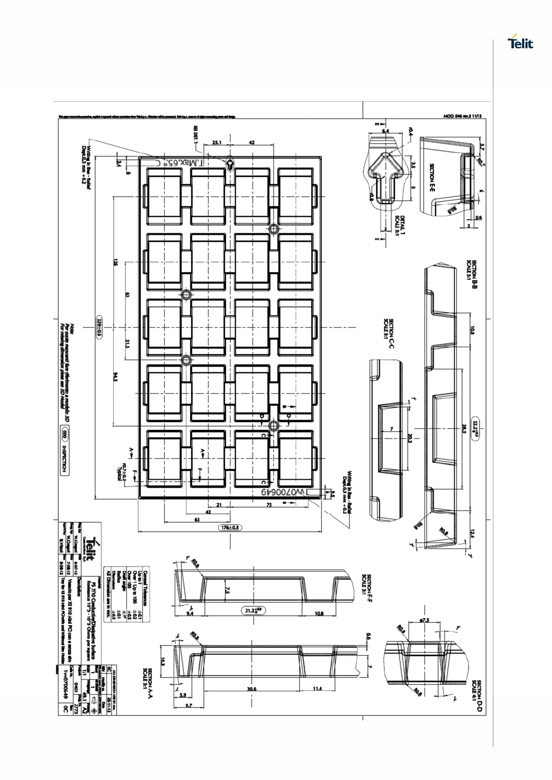
11. PACKAGING
Tray
The LM940 modules are packaged on trays of 20 pieces each. These trays can be used
in SMT processes for pick & place handling.
LM940 HW Design Guide
1VV0301352 Rev. 2 Page 57 of 68 2017-07-19

LM940 HW Design Guide
1VV0301352 Rev. 2 Page 58 of 68 2017-07-19
12. CONFORMITY ASSESSMENT ISSUES
Approvals
Fully type approved confirming with R&TTE directive
CE, GCF
FCC, IC, PTCRB
RoHS and REACH
Approvals for major Mobile Network Operators
Declaration of Conformity
The DoC is available here: www.telit.com/RED/
FCC certificates
The FCC Certifcate is available here: www.fcc.gov/oet/ea/fccid
IC certificates
The IC Certifcate is available here:
https://sms-sgs.ic.gc.ca/equipmentSearch/searchRadioEquipments?execution=e1s1&lang=en
FCC/IC Regulatory notices
Modification statement
Telit has not approved any changes or modifications to this device by the user. Any changes
or modifications could void the user’s authority to operate the equipment.
Telit n’approuve aucune modification apportée à l’appareil par l’utilisateur, quelle qu’en soit
la nature. Tout changement ou modification peuvent annuler le droit d’utilisation de
l’appareil par l’utilisateur.
Interference statement
This device complies with Part 15 of the FCC Rules and Industry Canada licence-exempt
RSS standard(s). Operation is subject to the following two conditions: (1) this device may
not cause interference, and (2) this device must accept any interference, including
interference that may cause undesired operation of the device.
Le présent appareil est conforme aux CNR d'Industrie Canada applicables aux appareils
radio exempts de licence. L'exploitation est autorisée aux deux conditions suivantes : (1)
l'appareil ne doit pas produire de brouillage, et (2) l'utilisateur de l'appareil doit accepter tout

LM940 HW Design Guide
1VV0301352 Rev. 2 Page 59 of 68 2017-07-19
brouillage radioélectrique subi, même si le brouillage est susceptible d'en compromettre le
fonctionnement.
RF exposure
This equipment complies with FCC and ISED radiation exposure limits set forth for an
uncontrolled environment. The antenna should be installed and operated with minimum
distance of 20 cm between the radiator and your body. Antenna gain must be below:
Cet appareil est conforme aux limites d'exposition aux rayonnements de l’ISED pour un
environnement non contrôlé. L'antenne doit être installé de façon à garder une distance
minimale de 20 centimètres entre la source de rayonnements et votre corps. Gain de
l'antenne doit être ci-dessous:
WCDMA / LTE Antenna (except Band 30)
Brand : HNS (HANKOOK Network Solution)
Model Number : WE14-LF-07
Type : Dipole Antenna
LTE Antenna for Band 30
Brand : SAE HAN ANTENNA CO.,LTD
Model Number : DH-23T-ANT
Type : Dipole Antenna
Mode Band Antenna Gain (dBi)
LTE FDD 2100 – B1
FDD 1900 PCS – B2
FDD 1800+ – B3
FDD 1800 AWS-1 – B4
FDD 850 – B5
FDD 2600 – B7
FDD 900 – B8
FDD 700a – B12
FDD 700c – B13
FDD 700b – B17
FDD 800 – B20
3.5
3.5
3.5
3.5
3.0
4.0
3.0
3.0
3.0
3.0
3.0

LM940 HW Design Guide
1VV0301352 Rev. 2 Page 60 of 68 2017-07-19
FDD 1900+ – B25
FDD 850+ – B26
FDD 700 APT – B28
FDD 700d – B29
FDD 2300 WCS – B30
FDD AWS-3 – B66
TDD 2600 – B38
TDD 2300 – B40
TDD 2500 – B41
3.5
3.0
3.0
3.0
1.5
3.5
4.0
4.0
4.0
WCDMA 2100 – B1
1900 PCS – B2
1800 AWS-1 – B4
850 – B5
900 – B8
3.5
3.5
3.5
3.0
3.0
This transmitter must not be co-located or operating in conjunction with any other antenna
or transmitter.
L'émetteur ne doit pas être colocalisé ni fonctionner conjointement avec à autre antenne
ou autre émetteur.
FCC Class B digital device notice
This equipment has been tested and found to comply with the limits for a Class B digital
device, pursuant to part 15 of the FCC Rules. These limits are designed to provide
reasonable protection against harmful interference in a residential installation. This
equipment generates, uses and can radiate radio frequency energy and, if not installed and
used in accordance with the instructions, may cause harmful interference to radio
communications. However, there is no guarantee that interference will not occur in a
particular installation. If this equipment does cause harmful interference to radio or
television reception, which can be determined by turning the equipment off and on, the user
is encouraged to try to correct the interference by one or more of the following measures:
Reorient or relocate the receiving antenna.
Increase the separation between the equipment and receiver.
Connect the equipment into an outlet on a circuit different from that to which the
receiver is connected.

LM940 HW Design Guide
1VV0301352 Rev. 2 Page 61 of 68 2017-07-19
Consult the dealer or an experienced radio/TV technician for help.
Labelling Requirements for the Host device
The host device shall be properly labelled to identify the modules within the host device.
The certification label of the module shall be clearly visible at all times when installed in the
host device, otherwise the host device must be labelled to display the FCC ID and ISED of
the module, preceded by the words "Contains transmitter module", or the word "Contains",
or similar wording expressing the same meaning, as follows:
L'appareil hôte doit être étiqueté comme il faut pour permettre l'identification des modules
qui s'y trouvent. L'étiquette de certification du module donné doit être posée sur l'appareil
hôte à un endroit bien en vue en tout temps. En l'absence d'étiquette, l'appareil hôte doit
porter une étiquette donnant le FCC ID et l’ISED du module, précédé des mots « Contient
un module d'émission », du mot « Contient » ou d'une formulation similaire exprimant le
même sens, comme suit :
LM940
Contains FCC ID: RI7LM940
Contains IC: 5131A-LM940
CAN ICES-3 (B) / NMB-3 (B)
This Class B digital apparatus complies with Canadian ICES-003.
Cet appareil numérique de classe B est conforme à la norme canadienne ICES-003.

LM940 HW Design Guide
1VV0301352 Rev. 2 Page 62 of 68 2017-07-19
13. SAFETY RECOMMENDATIONS
READ CAREFULLY
Be sure the use of this product is allowed in the country and in the environment required.
The use of this product may be dangerous and has to be avoided in the following areas:
Where it can interfere with other electronic devices in environments such as
hospitals, airports, aircrafts, etc.
Where there is risk of explosion such as gasoline stations, oil refineries, etc. It is the
responsibility of the user to enforce the country regulation and the specific
environment regulation.
Do not disassemble the product; any mark of tampering will compromise the warranty
validity. We recommend following the instructions of the hardware user guides for correct
wiring of the product. The product has to be supplied with a stabilized voltage source and
the wiring has to be conformed to the security and fire prevention regulations. The product
has to be handled with care, avoiding any contact with the pins because electrostatic
discharges may damage the product itself. Same cautions have to be taken for the SIM,
checking carefully the instruction for its use. Do not insert or remove the SIM when the
product is in power saving mode.
The system integrator is responsible for the functioning of the final product; therefore, care
has to be taken to the external components of the module, as well as any project or
installation issue, because the risk of disturbing the GSM network or external devices or
having impact on the security. Should there be any doubt, please refer to the technical
documentation and the regulations in force. Every module has to be equipped with a proper
antenna with specific characteristics. The antenna has to be installed with care in order to
avoid any interference with other electronic devices and has to guarantee a minimum
distance from the body (20 cm). In case this requirement cannot be satisfied, the system
integrator has to assess the final product against the SAR regulation.
The European Community provides some Directives for the electronic equipment
introduced on the market. All of the relevant information is available on the European
Community website:
http://europa.eu.int/comm/enterprise/rtte/dir99-5.htm
The text of the Directive 99/05 regarding telecommunication equipment is available,
while the applicable Directives (Low Voltage and EMC) are available at:
http://europa.eu.int/comm/enterprise/rtte/dir99-5.htm

LM940 HW Design Guide
1VV0301352 Rev. 2 Page 63 of 68 2017-07-19
14. REFERENCE TABLE OF RF BANDS CHARACTERISTICS
RF Bands Characteristics
Mode Freq. Tx
(MHz)
Freq. Rx
(MHz)
Channels Tx-Rx
Offset
WCDMA 2100 –
B1
1920 ~ 1980 2110 ~ 2170 Tx: 9612 ~ 9888
Rx: 10562 ~ 10838
190 MHz
WCDMA 1900 –
B2
1850 ~ 1910 1930 ~ 1990 Tx: 9262 ~ 9538
Rx: 9662 ~ 9938
80 MHz
WCDMA AWS –
B4
1710 ~ 1755 2110 ~ 2155 Tx: 1537 ~ 1738
Rx: 1312 ~ 1513
400 MHz
WCDMA 850 – B5 824 ~ 849 869 ~ 894 Tx: 4132 ~ 4233
Rx: 4357 ~ 4458
45 MHz
WCDMA 900 – B8 880 ~ 915 925 ~ 960 Tx: 2712 ~ 2863
Rx: 2937 ~ 3088
45 MHz
LTE 2100 – B1 1920 ~ 1980 2110 ~ 2170 Tx: 18000 ~ 18599
Rx: 0 ~ 599
190 MHz
LTE 1900 – B2 1850 ~ 1910 1930 ~ 1990 Tx: 18600 ~ 19199
Rx: 600 ~ 1199
80 MHz
LTE 1800+ – B3 1710 ~ 1785 1805 ~ 1880 Tx: 19200 ~ 19949
Rx: 1200 ~ 1949
95 MHz
LTE AWS-1 – B4 1710 ~ 1755 2110 ~ 2155 Tx: 19950 ~ 20399
Rx: 1950 ~ 2399
400 MHz
LTE 850 – B5 824 ~ 849 869 ~ 894 Tx: 20400 ~ 20649
Rx: 2400 ~ 2649
45 MHz
LTE 2600 – B7 2500 ~ 2570 2620 ~ 2690 Tx: 20750 ~ 21449
Rx: 2750 ~ 3449
120 MHz
LTE 900 – B8 880 ~ 915 925 ~ 960 Tx: 21450 ~ 21799
Rx: 3450 ~ 3799
45 MHz
LTE 700a – B12 699 ~ 716 729 ~ 746 Tx : 23010 ~ 23179
Rx : 5010 ~ 5179
30 MHz
LTE 700c – B13 777 ~ 787 746 ~ 756 Tx : 27210 ~ 27659
Rx : 9210 ~ 9659
-31 MHz

LM940 HW Design Guide
1VV0301352 Rev. 2 Page 64 of 68 2017-07-19
Mode Freq. Tx
(MHz)
Freq. Rx
(MHz)
Channels Tx-Rx
Offset
LTE 700b – B17 704 ~ 716 734 ~ 746 Tx: 23730 ~ 23849
Rx: 5730 ~ 5849
30 MHz
LTE 800 – B20 832 ~ 862 791 ~ 821 Tx: 24150 ~ 24449
Rx: 6150 ~ 6449
-41 MHz
LTE 1900+ – B25 1850 ~ 1915 1930 ~ 1995 Tx: 8040 ~ 8689
Rx: 26040 ~ 26689
80 MHz
LTE 850+ – B26 814 ~ 849 859 ~ 894 Tx: 8690 ~ 9039
Rx: 26690 ~ 27039
45 MHz
LTE 700 APT –
B28
703 ~ 748 758 ~ 803 Tx: 9210 ~ 9659
Rx: 27210 ~ 27659
55 MHz
LTE 700 d – B29 Downlink
only
717 ~ 728 Rx: 9660 ~ 9769 –
LTE 2300 WCS –
B30
2305 ~ 2315 2350 ~ 2360 Tx: 9770 ~ 9869
Rx: 27660 ~ 27759
45 MHz
LTE AWS-3 – B66 1710 ~ 1780 2110 ~ 2200 Tx: 66436 ~ 67335
Rx: 131972 ~
132671
400 MHz
LTE TDD 2600 –
B38
2570 ~ 2620 2570 ~ 2620 Tx: 37750 ~ 38250
Rx: 37750 ~ 38250
0 MHz
LTE TDD 2300 –
B40
2300 ~ 2400 2300 ~ 2400 Tx: 38650 ~ 39650
Rx: 38650 ~ 39650
0 MHz
LTE TDD 2500 –
B41
2496 ~ 2690 2496 ~ 2690 Tx: 39650 ~ 41589
Rx: 39650 ~ 41589
0 MHz

LM940 HW Design Guide
1VV0301352 Rev. 2 Page 65 of 68 2017-07-19
15. ACRONYMS
TTSC Telit Technical Support Centre
USB Universal Serial Bus
HS High Speed
DTE Data Terminal Equipment
UMTS Universal Mobile Telecommunication System
WCDMA Wideband Code Division Multiple Access
HSDPA High Speed Downlink Packet Access
HSUPA High Speed Uplink Packet Access
UART Universal Asynchronous Receiver Transmitter
HSIC High Speed Inter Chip
SIM Subscriber Identification Module
SPI Serial Peripheral Interface
ADC Analog – Digital Converter
DAC Digital – Analog Converter
I/O Input Output
GPIO General Purpose Input Output
CMOS Complementary Metal – Oxide Semiconductor
MOSI Master Output – Slave Input
MISO Master Input – Slave Output
CLK Clock
MRDY Master Ready

LM940 HW Design Guide
1VV0301352 Rev. 2 Page 66 of 68 2017-07-19
SRDY Slave Ready
CS Chip Select
RTC Real Time Clock
PCB Printed Circuit Board
ESR Equivalent Series Resistance
VSWR Voltage Standing Wave Radio
VNA Vector Network Analyzer
FDD Frequency division duplex
I2C Inter-integrated circuit
LTE Long term evolution
SOC System-on-Chip

LM940 HW Design Guide
1VV0301352 Rev. 2 Page 67 of 68 2017-07-19
16. DOCUMENT HISTORY
Revision Date Changes
0 2017-01-17 First Draft
1 2017-06-23 Changed document form
2 2017-07-19 Updated 7. RF section
Updated 12.5 RF exposure

[01.2017]
Mod.0818 2017-01 Rev.0