Telit Communications S p A WE865D Wi-Fi 802.11 b/g Module User Manual Gxzzz Product Description
Telit Communications S.p.A. Wi-Fi 802.11 b/g Module Gxzzz Product Description
UserManual.wiki
>
Telit Communications S p A
>
WE865D User Manual
>
Hardware Manual
Contents
1.
Hardware Manual
2.
Software Manual
Hardware Manual
Navigation menu
Upload a User Manual
Namespaces
Wiki Guide
HTML
PDF
Info
Views
User Manual
Discussion / Help
Navigation
![WE865-DUAL HW User Guide 1vv0300787 Rev. 1 - 03/10/08 Reproduction forbidden without Telit Communications S.p.A. written authorization - All Rights Reserved page 7 of 48 1.1 Related documents The following documents are related to this user guide: [1] Telit WE865-DUAL Product Description 80312ST10046A [2] Telit WE865-DUAL Software User Guide 1vv0300788 [3] Telit GE863-PRO³ Hardware User Guide 1vv0300773a [4] Telit GE863-PRO³ Software User Guide 1vv0300788 [5] Telit GE863PRO3 EVK User Guide 1vv0300776 [6] Telit GE863PRO3 Linux SW User Guide 1vv0300781 [7] Telit GE863PRO3Linux Development Environment User Guide1vv0300780 All documentation can be downloaded from Telit’s official web site www.telit.com if not otherwise indicated.](https://usermanual.wiki/Telit-Communications-S-p-A/WE865D.Hardware-Manual/User-Guide-1022522-Page-7.png)
![WE865-DUAL HW User Guide 1vv0300787 Rev. 1 - 03/10/08 Reproduction forbidden without Telit Communications S.p.A. written authorization - All Rights Reserved page 10 of 48 3 Pin-out 3.1 Pin table Ball Signal I/O Function Internal PULL UP/DOWN Type SDIO A1 SDIO[0] I/O SDIO DATA[0] (or SPI MISO) 10KOhm pull-up SDIO (or SPI) B2 SDIO[1] I/O SDIO DATA[1] (or SPI INTERRUPT) 10KOhm pull-up SDIO (or SPI) A2 SDIO[2] I/O SDIO DATA[2] 10KOhm pull-up SDIO B3 SDIO[3] I/O SDIO DATA[3] (or SPI CHIP SELECT) 10KOhm pull-up SDIO (or SPI) A3 SDIO_CLK I/O SDIO CLOCK (or SPI CLOCK) - SDIO (or SPI) A4 SDIO_CMD I/O SDIO CMD (or SPI MOSI ) 10KOhm pull-up SDIO (or SPI) Testing and Certification C3 TEST_1 O Test line n. 1 - TEST C4 TEST_2 I Test line n. 2 - TEST C5 TEST_3 I Test line n. 3 - TEST D5 TEST_4 I Test line n. 4 - TEST Miscellaneous Functions B1 EN_A* I Enable/shut-down 10KOhm pull-up control C1 MR_RESET* I Manual reset 100KOhm pull-up control D1 EN_B* I Enable/shut-down 10KOhm pull-up control D2 RESET I Reset for host processor 47KOhm pull-down control H5 RF_ANT RF RF output - antenna Power Supply E1 VDD PWR Power input pin - power supply E2 VDD PWR Power input pin - power supply F1 VCC_A PWR Power input pin - power supply F2 VCC_A PWR Power input pin - power supply F3 VCC_A PWR Power input pin - power supply RESERVED1 A5 N.C. A6 N.C. 1 All the reserved pins must be kept not connected (N.C.)](https://usermanual.wiki/Telit-Communications-S-p-A/WE865D.Hardware-Manual/User-Guide-1022522-Page-10.png)
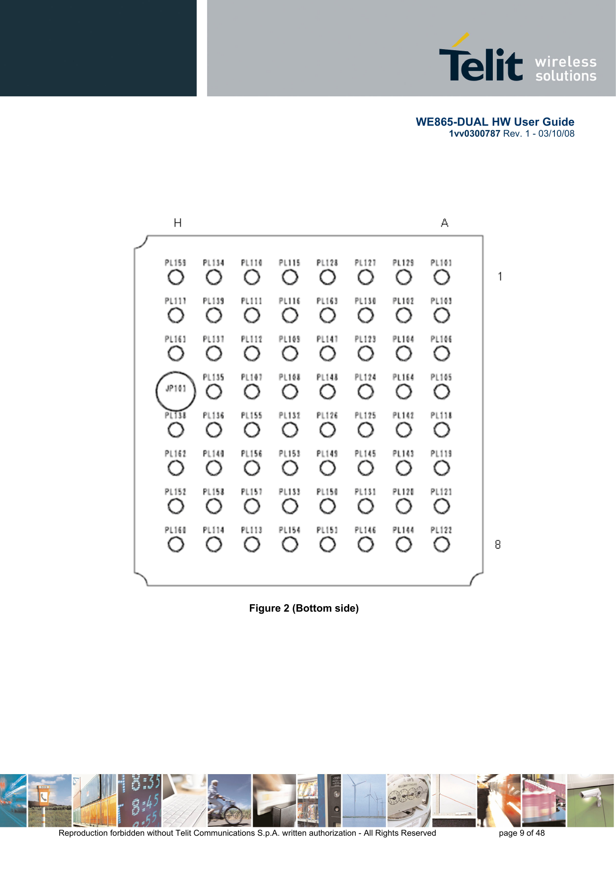
![WE865-DUAL HW User Guide 1vv0300787 Rev. 1 - 03/10/08 Reproduction forbidden without Telit Communications S.p.A. written authorization - All Rights Reserved page 12 of 48 3.2 Ball grid A B C D E F G H 1 SDIO[0] EN_A* MR_RESET* EN_B* VDD VCC_A GND NC 2 SDIO[2] SDIO[1] GND RESET VDD VCC_A NC NC 3 SDIO_CLK SDIO[3] TEST_1 NC NC VCC_A GND GND 4 SDIO_CMD NC TEST_2 NC NC NC GND NC 5 NC NC TEST_3 TEST_4 GND NC GND RF_ANT 6 NC NC NC NC NC NC NC GND 7 NC NC GND NC GND NC NC NC 8 NC NC NC NC NC NC NC NC Table 2 NOTE: The drawing above is a top view.](https://usermanual.wiki/Telit-Communications-S-p-A/WE865D.Hardware-Manual/User-Guide-1022522-Page-12.png)
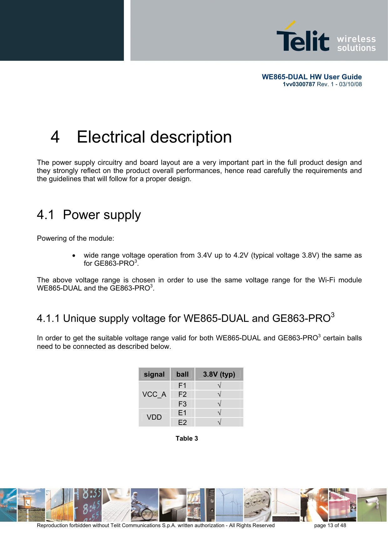
![WE865-DUAL HW User Guide 1vv0300787 Rev. 1 - 03/10/08 Reproduction forbidden without Telit Communications S.p.A. written authorization - All Rights Reserved page 14 of 48 Figure 3 The table below shows the operating and absolute voltage ranges. VOLTAGE RANGES @ 25 °C Min [V] Typ [V] Max [V] Operating range 3.4 3.8 4.2 Table 4 VCC_A (F1)VCC_A (F2)VCC_A (F3)3.8 V (typ) VDD (E1)VDD (E2)WE865-DUAL](https://usermanual.wiki/Telit-Communications-S-p-A/WE865D.Hardware-Manual/User-Guide-1022522-Page-14.png)
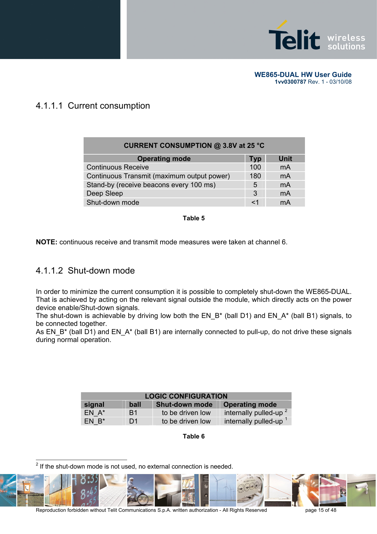
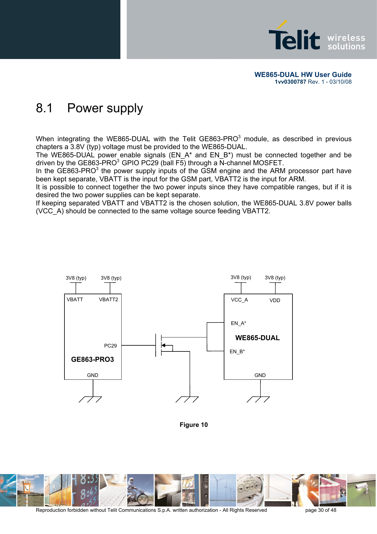
![WE865-DUAL HW User Guide 1vv0300787 Rev. 1 - 03/10/08 Reproduction forbidden without Telit Communications S.p.A. written authorization - All Rights Reserved page 16 of 48 VOLTAGE LEVELS @ 25 °C VIL SIGNAL Min [V] Max [V] EN_A*, EN_B* 0 0.20 Table 7 Figure 4 4.2 Power supply design guidelines The power supply circuitry is a very important part in the full product design and it strongly affects the product overall performances, hence read carefully the requirements and the guidelines that will follow for a proper design. The table below shows the WE865-DUAL operating voltage range: VOLTAGE RANGE Nominal Supply Voltage 3.8V Minimum Supply Voltage 3.4V Max Supply Voltage 4.2V Table 8 The electrical design of the power supply strongly depends on the power source the current is drained from. Please refer to electrical design guidelines in the GE863-PRO3 Hardware User Guide for further information. WE865-DUAL EN_B* EN_A*](https://usermanual.wiki/Telit-Communications-S-p-A/WE865D.Hardware-Manual/User-Guide-1022522-Page-16.png)
![WE865-DUAL HW User Guide 1vv0300787 Rev. 1 - 03/10/08 Reproduction forbidden without Telit Communications S.p.A. written authorization - All Rights Reserved page 21 of 48 4.3.1 Reset An active high host reset (RESET, ball D2), allowing the WE865-DUAL to be reset by an external device (host). This pin is internally pulled-down, do not drive the signal during normal operation. The signal must be asserted for a period greater than 1ms. VOLTAGE LEVELS @ 25 °C Min [V] Max [V] Remark VIH 2,0 3,0 - Table 9 Figure 7 WE865-DUAL RESET](https://usermanual.wiki/Telit-Communications-S-p-A/WE865D.Hardware-Manual/User-Guide-1022522-Page-21.png)
![WE865-DUAL HW User Guide 1vv0300787 Rev. 1 - 03/10/08 Reproduction forbidden without Telit Communications S.p.A. written authorization - All Rights Reserved page 22 of 48 4.3.2 Manual reset An active low manual reset (MR_RESET*, ball C1), see the table below for the allowed voltage levels. As the pin is internally pulled-up, do not drive the signal during normal operation. The signal must be asserted for a period greater than 1ms. VOLTAGE LEVELS @ 25 °C Min [V] Max [V] Remark VIL -0,3 0,825 Table 10 Figure 8 WE865-DUAL MR_RESET*](https://usermanual.wiki/Telit-Communications-S-p-A/WE865D.Hardware-Manual/User-Guide-1022522-Page-22.png)
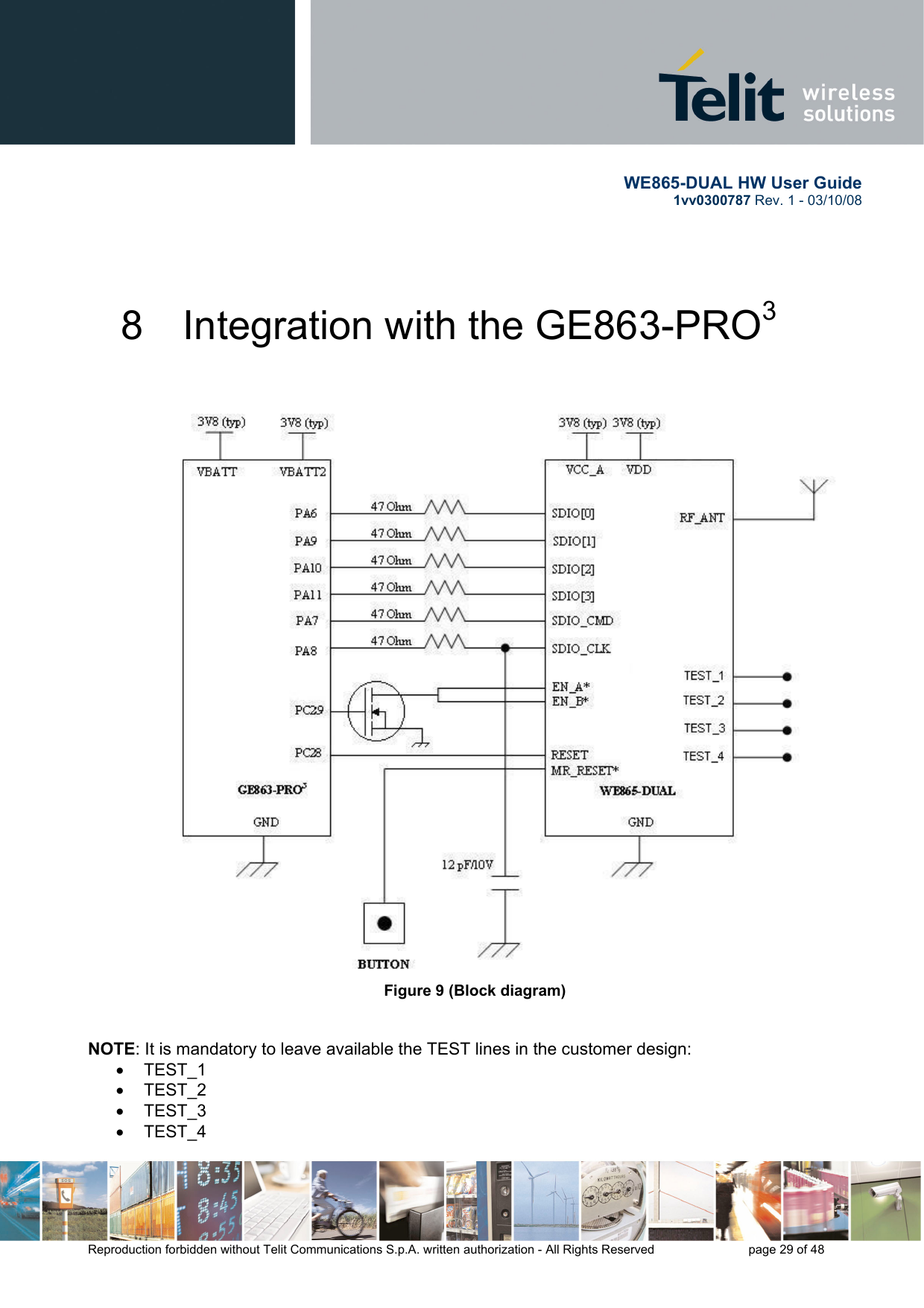
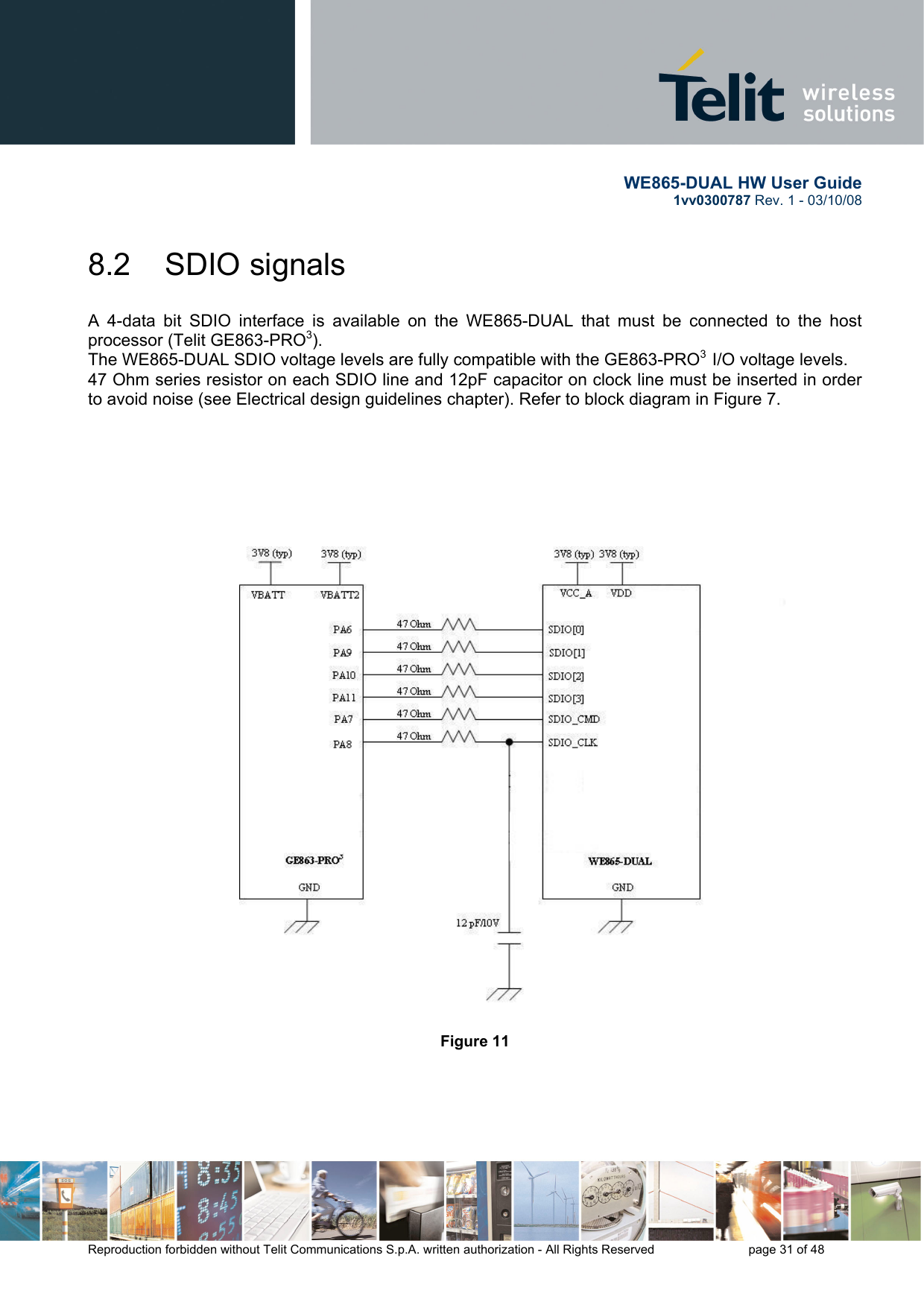
![WE865-DUAL HW User Guide 1vv0300787 Rev. 1 - 03/10/08 Reproduction forbidden without Telit Communications S.p.A. written authorization - All Rights Reserved page 23 of 48 4.4 SDIO signals A 4-data bit SDIO interface is available on the WE865-DUAL that must be connected to the host processor (Telit GE863-PRO3). WE865-DUAL SDIO voltage levels are fully compatible with the GE863-PRO3 I/O voltage levels. 47 Ohm series resistor on each SDIO line and 12pF capacitor on clock line must be inserted in order to avoid noise (see Electrical design guidelines chapter). Refer to §8.2. Voltage levels for all the SDIO pins are reported in the table: VOLTAGE LEVELS @ 25 °C Min [V] Max [V] Remark VIL -0,3 0,825 VIH 2,0625 3,6 VOL 0 0,125 I = 4mA VOH 2,475 3,3 I = 4mA Table 11](https://usermanual.wiki/Telit-Communications-S-p-A/WE865D.Hardware-Manual/User-Guide-1022522-Page-23.png)
![WE865-DUAL HW User Guide 1vv0300787 Rev. 1 - 03/10/08 Reproduction forbidden without Telit Communications S.p.A. written authorization - All Rights Reserved page 26 of 48 7 Antenna The antenna connection and board layout design are the most important part in the full product design and they strongly reflect on the product overall performances, hence read carefully and follow the requirements and the guidelines for a proper design. 7.1 Wi-Fi antenna guidelines General guidelines for an antenna and antenna line on PCB for a Telit WE865-DUAL device ANTENNA REQUIREMENTS Frequency range [MHz] 2400-2500 Gain [dBi] ≤ 2 Impedance [Ohm] 50 Maximum Input Power [mW] >100 VSWR recommended ≤2 Table 12 Frequency range indicated in order to support 14 Wi-Fi channels. Smaller ranges are allowed or requested for application over 11 or 13 channels. Please refer to IEEE specifications and to the proper regulatory body directives about 802.11 channels and antenna specifications in different countries. When using the Telit WE865-DUAL, since there's no antenna connector on the module, the antenna must be connected to the WE865-DUAL through the PCB with the antenna pad. Please consider that antenna design and choice is dependent on the specific application.](https://usermanual.wiki/Telit-Communications-S-p-A/WE865D.Hardware-Manual/User-Guide-1022522-Page-26.png)
![WE865-DUAL HW User Guide 1vv0300787 Rev. 1 - 03/10/08 Reproduction forbidden without Telit Communications S.p.A. written authorization - All Rights Reserved page 27 of 48 This transmission line shall fulfill the following requirements: ANTENNA LINE ON PCB REQUIREMENTS Impedance [Ohm] 50 Maximum Attenuation [dB] 0.3 Coupling with other signals is not allowed Table 13 7.2 Wi-Fi antenna PCB trace guidelines • Ensure that the antenna line impedance is 50 ohm. • Keep the antenna line on the PCB as short as possible in order to limit losses. • Antenna line must have uniform characteristics, constant cross section, avoid meanders and abrupt curves. • Keep, if possible, one layer of the PCB used only for the Ground plane. • Surround (on the sides, over and under) the antenna line on PCB with Ground, avoid having other signal tracks facing directly the antenna line track. • The ground around the antenna line on PCB has to be strictly connected to the Ground Plane by placing vias once per 2mm at least. • Place EM noisy devices as far as possible from WE865-DUAL antenna line. • Keep the antenna line far away from the WE865-DUAL power supply lines. • If you have EM noisy devices around the PCB hosting the WE865-DUAL, such as fast switching ICs, take care of the shielding of the antenna line by burying it inside the layers of PCB and surround it with Ground planes, or shield it with a metal frame cover. • If you don't have EM noisy devices around the PCB of WE865-DUAL, by using a strip-line on the superficial copper layer for the antenna line, the line attenuation will be lower than a buried one.](https://usermanual.wiki/Telit-Communications-S-p-A/WE865D.Hardware-Manual/User-Guide-1022522-Page-27.png)
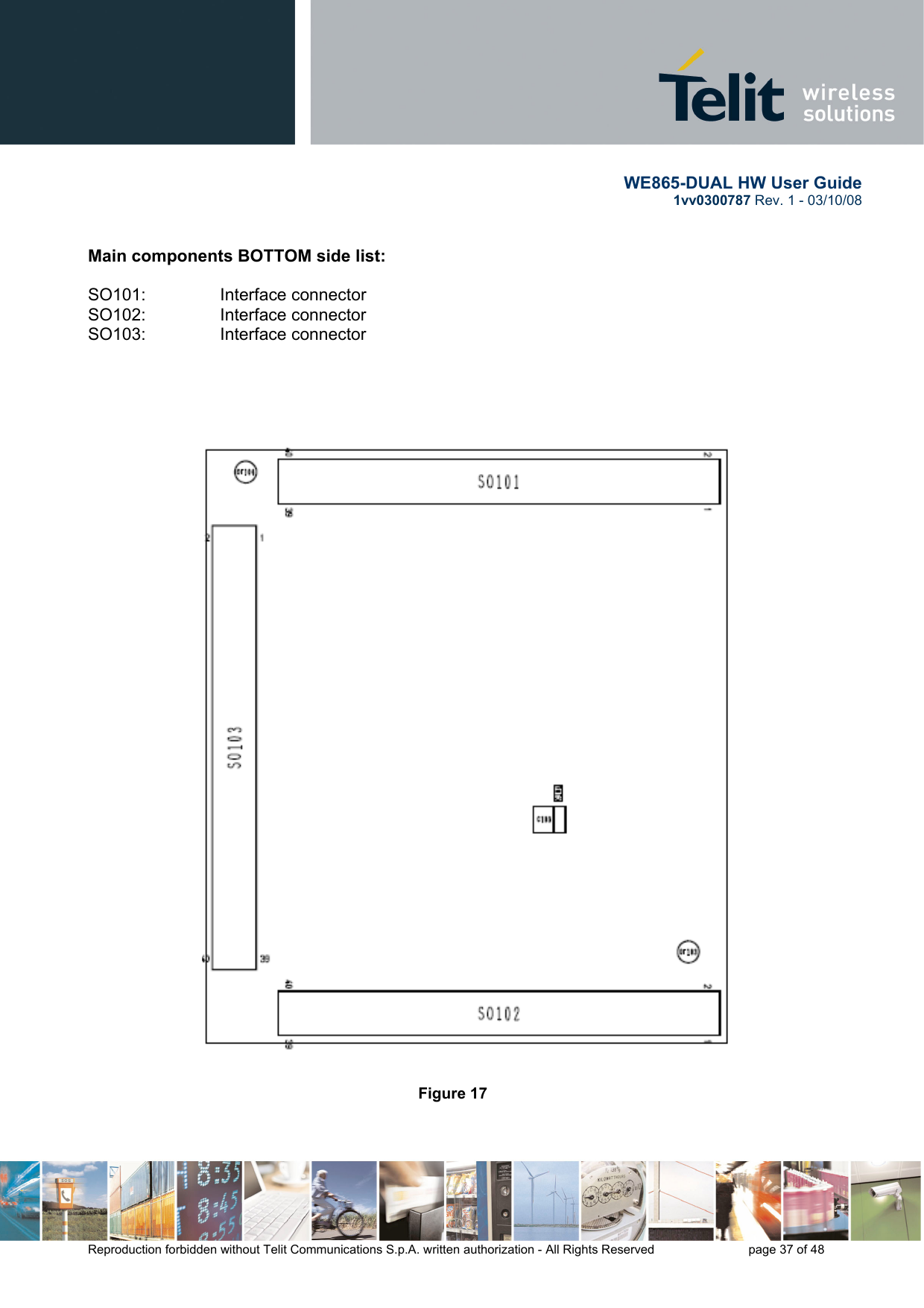
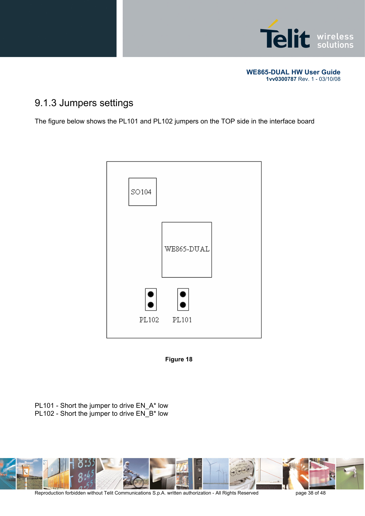
![WE865-DUAL HW User Guide 1vv0300787 Rev. 1 - 03/10/08 Reproduction forbidden without Telit Communications S.p.A. written authorization - All Rights Reserved page 39 of 48 9.1.4 Pin table SO101 SO102 SO103 PL103 Pin n. Signal name Signal name Signal name Signal name 1 RESERVED RESERVED RESERVED TEST_1 2 RESERVED RESERVED RESERVED TEST_2 3 RESERVED RESERVED RESERVED TEST_3 4 RESERVED RESERVED RESERVED TEST_4 5 RESERVED RESERVED RESERVED GND 6 RESERVED RESERVED RESERVED - 7 SDIO[0] RESERVED RESERVED - 8 SDIO_CMD RESERVED RESERVED - 9 SDIO_CLK RESERVED RESERVED - 10 SDIO[1] RESERVED RESERVED - 11 SDIO[2] RESERVED RESERVED - 12 SDIO[3] RESERVED RESERVED - 13 RESERVED RESERVED RESERVED - 14 RESERVED RESERVED RESERVED - 15 RESERVED RESERVED RESERVED - 16 RESERVED RESERVED RESERVED - 17 RESERVED RESERVED RESERVED - 18 RESERVED RESERVED RESERVED - 19 RESERVED RESERVED RESERVED - 20 RESERVED RESERVED RESERVED - 21 RESERVED RESERVED RESERVED - 22 RESERVED RESERVED RESERVED - 23 RESERVED RESERVED RESERVED - 24 RESERVED RESERVED RESERVED - 25 RESERVED RESERVED RESERVED - 26 RESERVED RESERVED RESERVED - 27 RESERVED RESERVED RESERVED - 28 RESERVED RESERVED RESERVED - 29 RESERVED RESERVED RESET - 30 RESERVED RESERVED RESERVED - 31 RESERVED RESERVED RESERVED - 32 RESERVED RESERVED RESERVED - 33 RESERVED RESERVED RESERVED - 34 RESERVED RESERVED RESERVED - 35 RESERVED RESERVED RESERVED - 36 VBATT RESERVED RESERVED - 37 RESERVED RESERVED GND - 38 RESERVED RESERVED RESERVED - 39 GND GND GND - 40 GND GND RESERVED - Table 14](https://usermanual.wiki/Telit-Communications-S-p-A/WE865D.Hardware-Manual/User-Guide-1022522-Page-39.png)
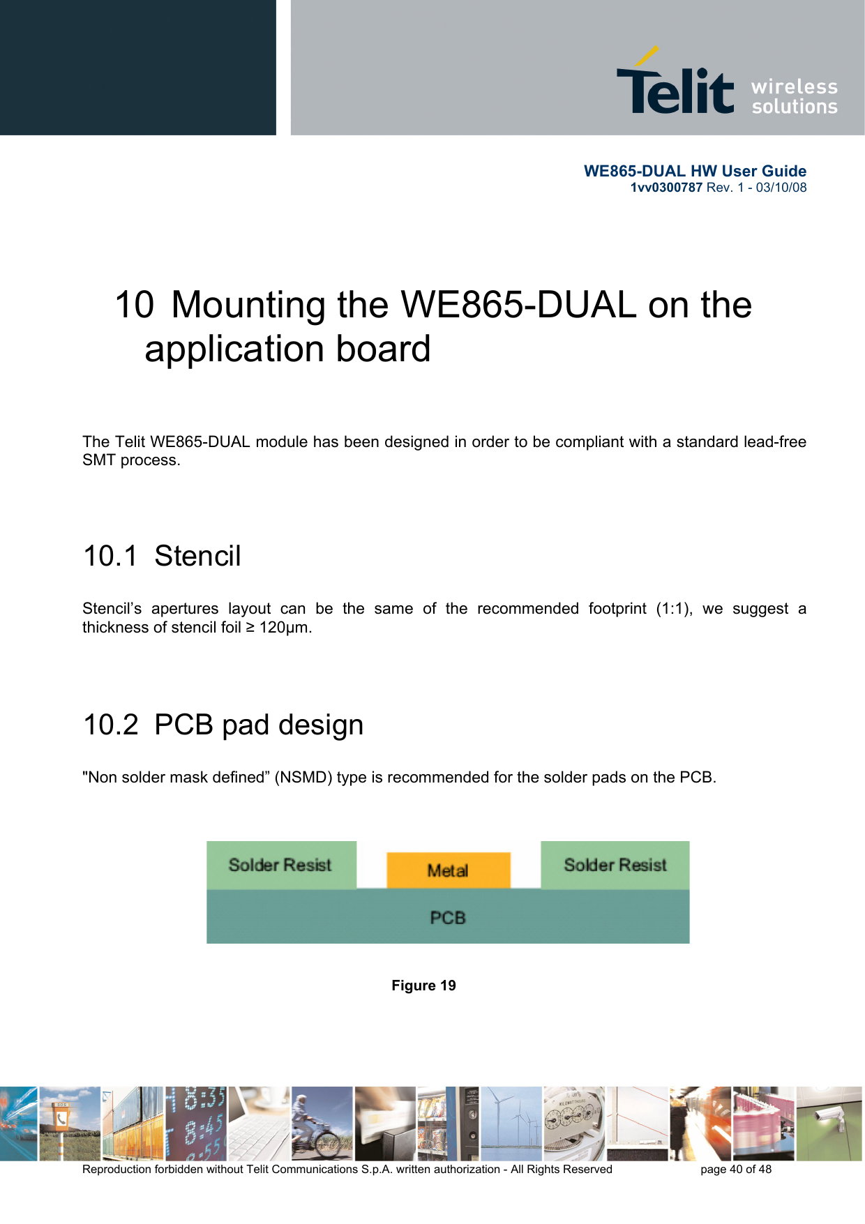
![WE865-DUAL HW User Guide 1vv0300787 Rev. 1 - 03/10/08 Reproduction forbidden without Telit Communications S.p.A. written authorization - All Rights Reserved page 41 of 48 Figure 20 Recommendations for PCB pad dimensions Dimension Value [mm] Ball pitch 2 Solder resist opening diameter A 1,150 Metal PAD diameter B 1 +/- 0,05 Table 15 Placement of microvias not covered by solder resist is not recommended inside the “Solder resist Opening”,unless the microvia carry the same signal of the pad itself.](https://usermanual.wiki/Telit-Communications-S-p-A/WE865D.Hardware-Manual/User-Guide-1022522-Page-41.png)
![WE865-DUAL HW User Guide 1vv0300787 Rev. 1 - 03/10/08 Reproduction forbidden without Telit Communications S.p.A. written authorization - All Rights Reserved page 42 of 48 Figure 21 Holes in pad are allowed only for blind holes and not for through holes. Recommendations for PCB pad surfaces: Finish Layer tickness [um] Properties Electro-less Ni / Immersion Au 3-7 / 0,05-0,15 good solder ability protection, high shear force values Table 16 The PCB must be able to resist the higher temperatures, which are occurring at the lead-free process. This issue should be discussed with the PCB-supplier. Generally, the wet-ability of tin-lead solder paste on the described surface plating is better compared to lead-free solder paste.](https://usermanual.wiki/Telit-Communications-S-p-A/WE865D.Hardware-Manual/User-Guide-1022522-Page-42.png)