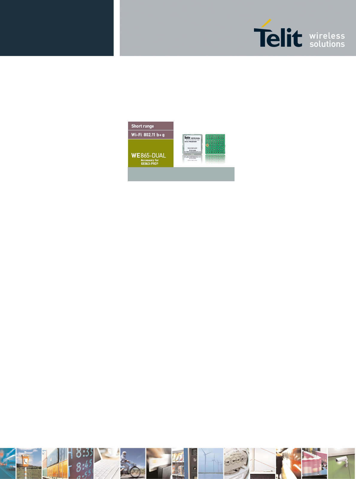
Telit Communications S p A WE865D Wi-Fi 802.11 b/g Module User Manual Gxzzz Product Description
Telit Communications S.p.A. Wi-Fi 802.11 b/g Module Gxzzz Product Description
Contents
- 1. Hardware Manual
- 2. Software Manual
Hardware Manual

WE865-DUAL Hardware User Guide
1vv0300787 Rev. 1 - 03/10/08
WE865-DUAL HW User Guide
1vv0300787 Rev. 1 - 03/10/08
Reproduction forbidden without Telit Communications S.p.A. written authorization - All Rights Reserved page 2 of 48
This document is relating to the following products:
WE865DUA000-001

WE865-DUAL HW User Guide
1vv0300787 Rev. 1 - 03/10/08
Reproduction forbidden without Telit Communications S.p.A. written authorization - All Rights Reserved page 3 of 48
Contents
1Overview ...........................................................................................................................6
1.1Related documents ................................................................................................................7
2Mechanical description....................................................................................................8
3Pin-out.............................................................................................................................10
3.1Pin table.................................................................................................................................10
3.2Ball grid .................................................................................................................................12
4Electrical description .....................................................................................................13
4.1Power supply ........................................................................................................................13
4.1.1Unique supply voltage for WE865-DUAL and GE863-PRO3......................................................... 13
4.1.1.1Current consumption ................................................................................................................. 15
4.1.1.2Shut-down mode........................................................................................................................ 15
4.2Power supply design guidelines.........................................................................................16
4.2.1+5V input source............................................................................................................................ 17
4.2.2+12V input source.......................................................................................................................... 18
4.2.3Battery source................................................................................................................................ 20
4.3Reset signals ........................................................................................................................20
4.3.1Reset.............................................................................................................................................. 21
4.3.2Manual reset .................................................................................................................................. 22
4.4SDIO signals .........................................................................................................................23
5Thermal design guidelines ............................................................................................24
6PCB layout design guidelines.......................................................................................25
7Antenna...........................................................................................................................26
7.1Wi-Fi antenna guidelines .....................................................................................................26
7.2Wi-Fi antenna PCB trace guidelines ...................................................................................27
7.3Wi-Fi antenna installation guidelines .................................................................................28
8Integration with the GE863-PRO3..................................................................................29
8.1Power supply ........................................................................................................................30
8.2SDIO signals .........................................................................................................................31
9WE865-DUAL - Evaluation kit........................................................................................32
9.1WE865-DUAL Interface board..............................................................................................35
9.1.1Mechanical description .................................................................................................................. 35
9.1.2Main components .......................................................................................................................... 36
9.1.3Jumpers settings............................................................................................................................ 38

WE865-DUAL HW User Guide
1vv0300787 Rev. 1 - 03/10/08
Reproduction forbidden without Telit Communications S.p.A. written authorization - All Rights Reserved page 4 of 48
9.1.4Pin table ......................................................................................................................................... 39
10Mounting the WE865-DUAL on the application board ................................................40
10.1Stencil....................................................................................................................................40
10.2PCB pad design ....................................................................................................................40
10.3Solder paste ..........................................................................................................................43
10.4Solder reflow.........................................................................................................................43
11Moisture sensitivity........................................................................................................45
12Conformity assessment issues ....................................................................................46
13Safety recommendations...............................................................................................47
14Document change log....................................................................................................48

WE865-DUAL HW User Guide
1vv0300787 Rev. 1 - 03/10/08
Reproduction forbidden without Telit Communications S.p.A. written authorization - All Rights Reserved page 5 of 48
DISCLAIMER
The information contained in this document is proprietary information of Telit Communications S.p.A.
including its affiliates (“TELIT”). The contents are confidential and any disclosure to persons other than
the Officers, employees, agents or subcontractors of the owner or licensee of this document, without
the prior written consent of Telit, is strictly prohibited.
Telit makes every effort to ensure the quality of the information it makes available. Notwithstanding the
foregoing, Telit does not make any warranty as to the information contained herein, and does not
accept any liability for any injury, loss or damage of any kind incurred by use of or reliance upon the
information.
Telit disclaims any and all responsibility for the application of the devices characterized in this
document, and notes that the application of the device must comply with the safety standards of the
applicable country, and where applicable, with the relevant wiring rules.
Telit reserves the right to make modifications, additions and deletions to this document due to
typographical errors, inaccurate information, or improvements to programs and/or equipment at any
time without a notice. Such changes will, nevertheless be incorporated into new editions of this
document.
All rights reserved.
© 2008 Telit Communications S.p.A.

WE865-DUAL HW User Guide
1vv0300787 Rev. 1 - 03/10/08
Reproduction forbidden without Telit Communications S.p.A. written authorization - All Rights Reserved page 6 of 48
1 Overview
This document is a user guide for developing a wireless application which integrates the Telit WE865-
DUAL with the GE863-PRO3 GSM/GPRS module creating a unique solution for a short and long
range.
This document cannot embrace the whole hardware solutions and products that may be designed.
The information given is a guide line and a starting point for properly developing products with the Telit
WE865-DUAL module.
For further hardware details please refer to the Telit “WE865-DUAL Product Description” document.
NOTICE
(EN) The integration of the Wi-Fi WE865-DUAL module within user application shall be done according
to the design rules described in this manual.
(IT) L’integrazione del modulo Wi-Fi WE865-DUAL all’interno dell’applicazione dell’utente dovrà
rispettare le indicazioni progettuali descritte in questo manuale.
(DE) Die integration des Wi-Fi WE865-DUAL Moduls in ein Gerät muß gemäß der in diesem Dokument
beschriebenen Kunstruktionsregeln erfolgen.
(SL) Integracija Wi-Fi WE865-DUAL modula v uporabniški aplikaciji bo morala upoštevati
projektna navodila, opisana v tem piročniku.
(SP) La utilización del modulo Wi-Fi WE865-DUAL debe ser conforme a los usos para los cuales ha
sido deseñado descritos en este manual del usuario.
(FR) L’intégration du module Wi-Fi WE865-DUAL dans l’application de l’utilisateur
sera faite selon les règles de conception décri tes dans ce manuel.
ה םדומ לש היצרגטניאה ךילהתהב הז ךמסמב תוטרופמה תויחנהה תא םשייל שקבתמ רוטרגטניאה– Wi-Fi WE865-DUAL
רצומה םע
The information presented in this document is believed to be accurate and reliable. However, no responsibility is
Assumed by Telit Communications S.p.A. for its use, nor any infringement of patents or other rights of third
parties which may result from its use. No license is granted by implication or otherwise under any patent rights of
Telit Communications S.p.A. other than for circuitry embodied in Telit products. This document is subject to
change without notice.

WE865-DUAL HW User Guide
1vv0300787 Rev. 1 - 03/10/08
Reproduction forbidden without Telit Communications S.p.A. written authorization - All Rights Reserved page 7 of 48
1.1 Related documents
The following documents are related to this user guide:
[1] Telit WE865-DUAL Product Description 80312ST10046A
[2] Telit WE865-DUAL Software User Guide 1vv0300788
[3] Telit GE863-PRO³ Hardware User Guide 1vv0300773a
[4] Telit GE863-PRO³ Software User Guide 1vv0300788
[5] Telit GE863PRO3 EVK User Guide 1vv0300776
[6] Telit GE863PRO3 Linux SW User Guide 1vv0300781
[7] Telit GE863PRO3Linux Development Environment User Guide1vv0300780
All documentation can be downloaded from Telit’s official web site www.telit.com if not otherwise
indicated.
WE865-DUAL HW User Guide
1vv0300787 Rev. 1 - 03/10/08
Reproduction forbidden without Telit Communications S.p.A. written authorization - All Rights Reserved page 8 of 48
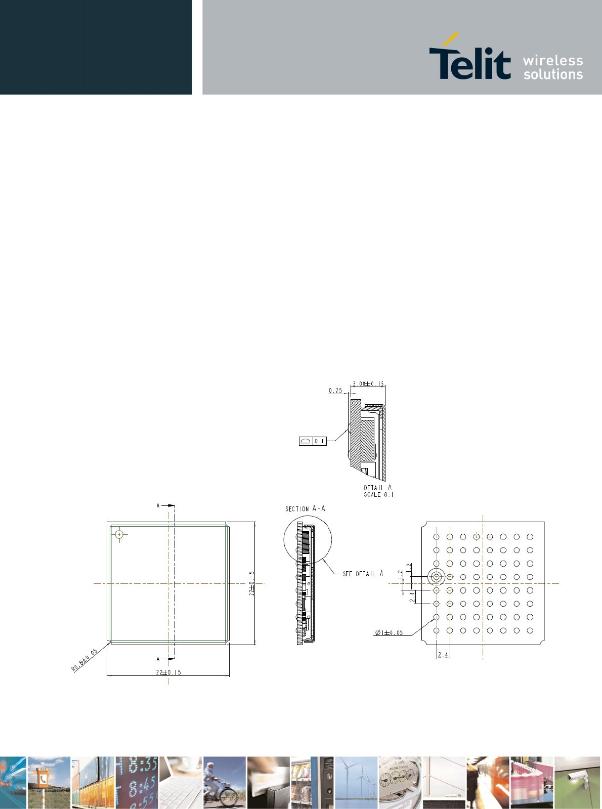
2 Mechanical description
The Telit WE865-DUAL module overall dimensions are:
• Length: 22.15 mm (max)
• Width: 22.15 mm (max)
• Thickness: 3.48 mm (max)
• Weight 3.5 g
Figure 1
WE865-DUAL HW User Guide
1vv0300787 Rev. 1 - 03/10/08
Reproduction forbidden without Telit Communications S.p.A. written authorization - All Rights Reserved page 9 of 48
Figure 2 (Bottom side)
WE865-DUAL HW User Guide
1vv0300787 Rev. 1 - 03/10/08
Reproduction forbidden without Telit Communications S.p.A. written authorization - All Rights Reserved page 10 of 48
3 Pin-out
3.1 Pin table
Ball Signal I/O Function Internal PULL
UP/DOWN Type
SDIO
A1 SDIO[0] I/O SDIO DATA[0] (or SPI MISO) 10KOhm pull-up SDIO (or SPI)
B2 SDIO[1]
I/O SDIO DATA[1]
(or SPI INTERRUPT) 10KOhm pull-up SDIO (or SPI)
A2 SDIO[2] I/O SDIO DATA[2] 10KOhm pull-up SDIO
B3 SDIO[3]
I/O SDIO DATA[3]
(or SPI CHIP SELECT) 10KOhm pull-up SDIO (or SPI)
A3 SDIO_CLK
I/O SDIO CLOCK
(or SPI CLOCK) - SDIO (or SPI)
A4 SDIO_CMD I/O SDIO CMD (or SPI MOSI ) 10KOhm pull-up SDIO (or SPI)
Testing and Certification
C3 TEST_1 O Test line n. 1 - TEST
C4 TEST_2 I Test line n. 2 - TEST
C5 TEST_3 I Test line n. 3 - TEST
D5 TEST_4 I Test line n. 4 - TEST
Miscellaneous Functions
B1 EN_A* I Enable/shut-down 10KOhm pull-up control
C1 MR_RESET* I Manual reset
100KOhm pull-
up control
D1 EN_B* I Enable/shut-down 10KOhm pull-up control
D2 RESET I Reset for host processor
47KOhm pull-
down control
H5 RF_ANT RF RF output - antenna
Power Supply
E1 VDD PWR Power input pin - power supply
E2 VDD PWR Power input pin - power supply
F1 VCC_A PWR Power input pin - power supply
F2 VCC_A PWR Power input pin - power supply
F3 VCC_A PWR Power input pin - power supply
RESERVED1
A5 N.C.
A6 N.C.
1 All the reserved pins must be kept not connected (N.C.)
WE865-DUAL HW User Guide
1vv0300787 Rev. 1 - 03/10/08
Reproduction forbidden without Telit Communications S.p.A. written authorization - All Rights Reserved page 11 of 48
Ball Signal I/O Function Internal PULL
UP/DOWN Type
A7 N.C.
A8 N.C.
B4 N.C.
B5 N.C.
B6 N.C.
B7 N.C.
B8 N.C.
C5 N.C.
C6 N.C.
C8 N.C.
D3 N.C.
D4 N.C.
D6 N.C.
D7 N.C.
D8 N.C.
E3 N.C.
E4 N.C.
E6 N.C.
E8 N.C.
F4 N.C.
F5 N.C.
F6 N.C.
F7 N.C.
F8 N.C.
G2 N.C.
G6 N.C.
G7 N.C.
G8 N.C.
H1 N.C.
H2 N.C.
H4 N.C.
H7 N.C.
H8 N.C.
Table 1
WE865-DUAL HW User Guide
1vv0300787 Rev. 1 - 03/10/08
Reproduction forbidden without Telit Communications S.p.A. written authorization - All Rights Reserved page 12 of 48
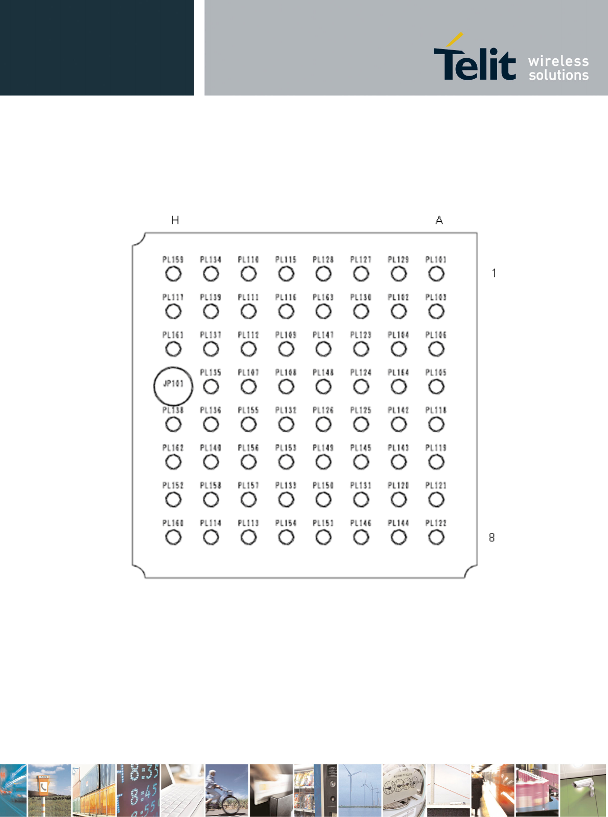
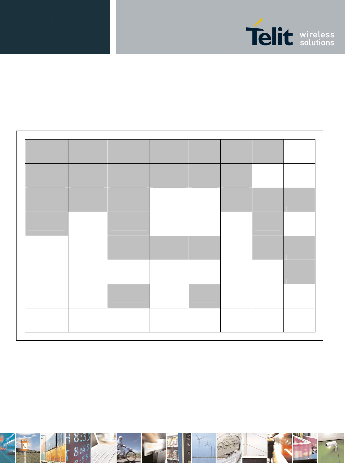
3.2 Ball grid
A B C D E F G H
1 SDIO[0] EN_A* MR_RESET* EN_B* VDD VCC_A GND NC
2 SDIO[2] SDIO[1] GND RESET VDD VCC_A NC NC
3 SDIO_CLK SDIO[3] TEST_1 NC NC VCC_A GND GND
4 SDIO_CMD NC TEST_2 NC NC NC GND NC
5 NC NC TEST_3 TEST_4 GND NC GND RF_ANT
6 NC NC NC NC NC NC NC GND
7 NC NC GND NC GND NC NC NC
8 NC NC NC NC NC NC NC NC
Table 2
NOTE: The drawing above is a top view.

WE865-DUAL HW User Guide
1vv0300787 Rev. 1 - 03/10/08
Reproduction forbidden without Telit Communications S.p.A. written authorization - All Rights Reserved page 13 of 48
4 Electrical description
The power supply circuitry and board layout are a very important part in the full product design and
they strongly reflect on the product overall performances, hence read carefully the requirements and
the guidelines that will follow for a proper design.
4.1 Power supply
Powering of the module:
• wide range voltage operation from 3.4V up to 4.2V (typical voltage 3.8V) the same as
for GE863-PRO3.
The above voltage range is chosen in order to use the same voltage range for the Wi-Fi module
WE865-DUAL and the GE863-PRO3.
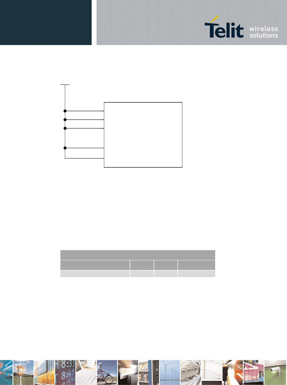
4.1.1 Unique supply voltage for WE865-DUAL and GE863-PRO3
In order to get the suitable voltage range valid for both WE865-DUAL and GE863-PRO3 certain balls
need to be connected as described below.
signal ball 3.8V (typ)
F1 √
F2 √
VCC_A
F3 √
E1 √
VDD E2 √
Table 3
WE865-DUAL HW User Guide
1vv0300787 Rev. 1 - 03/10/08
Reproduction forbidden without Telit Communications S.p.A. written authorization - All Rights Reserved page 14 of 48
Figure 3
The table below shows the operating and absolute voltage ranges.
VOLTAGE RANGES @ 25 °C
Min [V] Typ [V] Max [V]
Operating range 3.4 3.8 4.2
Table 4
VCC_A
(
F1
)
VCC
_
A
(
F2
)
VCC
_
A
(
F3
)
3.8 V (typ)
VDD
(
E1
)
VDD
(
E2
)
WE865-DUAL
WE865-DUAL HW User Guide
1vv0300787 Rev. 1 - 03/10/08
Reproduction forbidden without Telit Communications S.p.A. written authorization - All Rights Reserved page 15 of 48
4.1.1.1 Current consumption
CURRENT CONSUMPTION @ 3.8V at 25 °C
Operating mode Typ Unit
Continuous Receive 100 mA
Continuous Transmit (maximum output power) 180 mA
Stand-by (receive beacons every 100 ms) 5 mA
Deep Sleep 3 mA
Shut-down mode <1 mA
Table 5
NOTE: continuous receive and transmit mode measures were taken at channel 6.
4.1.1.2 Shut-down mode
In order to minimize the current consumption it is possible to completely shut-down the WE865-DUAL.
That is achieved by acting on the relevant signal outside the module, which directly acts on the power
device enable/Shut-down signals.
The shut-down is achievable by driving low both the EN_B* (ball D1) and EN_A* (ball B1) signals, to
be connected together.
As EN_B* (ball D1) and EN_A* (ball B1) are internally connected to pull-up, do not drive these signals
during normal operation.
LOGIC CONFIGURATION
signal ball Shut-down mode Operating mode
EN_A* B1 to be driven low internally pulled-up 2
EN_B* D1 to be driven low internally pulled-up 1
Table 6
2 If the shut-down mode is not used, no external connection is needed.
WE865-DUAL HW User Guide
1vv0300787 Rev. 1 - 03/10/08
Reproduction forbidden without Telit Communications S.p.A. written authorization - All Rights Reserved page 16 of 48
VOLTAGE LEVELS @ 25 °C
VIL
SIGNAL Min [V] Max [V]
EN_A*, EN_B* 0 0.20
Table 7
Figure 4
4.2 Power supply design guidelines
The power supply circuitry is a very important part in the full product design and it strongly affects the
product overall performances, hence read carefully the requirements and the guidelines that will follow
for a proper design.
The table below shows the WE865-DUAL operating voltage range:
VOLTAGE RANGE
Nominal Supply Voltage 3.8V
Minimum Supply Voltage 3.4V
Max Supply Voltage 4.2V
Table 8
The electrical design of the power supply strongly depends on the power source the current is drained
from. Please refer to electrical design guidelines in the GE863-PRO3 Hardware User Guide for further
information.
WE865-DUAL
EN_B*
EN_A*
WE865-DUAL HW User Guide
1vv0300787 Rev. 1 - 03/10/08
Reproduction forbidden without Telit Communications S.p.A. written authorization - All Rights Reserved page 17 of 48
4.2.1 +5V input source
A linear regulator can be used to generate the 3.8V output voltage. When using a linear regulator, a
proper heat sink shall be provided in order to dissipate the generated power. A protection diode should
be inserted close to the power input, in order to save the WE865-DUAL from power polarity inversion.
This can be the same diode as for spike protection.
The figure below shows a possible solution for the switching power supply. It must be taken into
account that the power supply performance strongly depends on the layout design.
Figure 5

WE865-DUAL HW User Guide
1vv0300787 Rev. 1 - 03/10/08
Reproduction forbidden without Telit Communications S.p.A. written authorization - All Rights Reserved page 18 of 48
4.2.2 +12V input source
Due to the big difference between the input source and the desired output voltage, a linear voltage
regulator is not suited and not recommended. A switching power supply will be preferable because of
its better efficiency especially in presence of peak current load.
When using a switching regulator, 500 kHz switching frequency (or more) is preferable because of its
smaller inductor size and its faster transient response. This allows the regulator to respond quickly to
any current peak absorption.
A protection diode should be inserted close to the power input, in order to save the WE865-DUAL from
power polarity inversion. This can be the same diode as for spike protection.
The figure below shows a possible solution for the switching power supply. It must be taken into
consideration that the switching power supply performances strongly depend on the layout design.
WE865-DUAL HW User Guide
1vv0300787 Rev. 1 - 03/10/08
Reproduction forbidden without Telit Communications S.p.A. written authorization - All Rights Reserved page 19 of 48
Figure 6

WE865-DUAL HW User Guide
1vv0300787 Rev. 1 - 03/10/08
Reproduction forbidden without Telit Communications S.p.A. written authorization - All Rights Reserved page 20 of 48
4.2.3 Battery source
The desired nominal output for the power supply is 3.8V and the maximum voltage allowed is 4.2V,
thus a single 3.7V Li-Ion cell battery type is suited for supplying the power to the WE865-DUAL
module.
Please refer to GE863-PRO3 electrical design guidelines for further information regarding type
and battery usage.
A protection diode should be inserted close to the power input, in order to save the WE865-DUAL from
power polarity inversion. Otherwise the battery connector should be done in a way to avoid polarity
inversions when connecting the battery.
When integrating the GE863-PRO3 with the WE865-DUAL modules together in the user application,
take into account that battery charger control circuitry is embedded inside the GE863-PRO3 (please
refer to GE863-PRO3 Hardware User Guide for more details) and can be used with Li-ION batteries
only. Using other type of batteries, an external charger will be needed.
The battery capacity should be suitable chosen dependently on the customer’s application current
consumption and the battery life requirements. When integrating the GE863-PRO3 with the WE865-
DUAL modules together in the user application, the battery capacity must be at least 800mAh in order
to withstand any current peak (please refer to GE863-PRO3 Hardware User Guide for more details).
4.3 Reset signals
The WE865-DUAL has a power-on-reset (POR) circuit inside, so no specific reset is required in the
initialization phase.
Two signals are available to reset the module:
• an active high host reset (RESET)
• an active low manual reset (MR_RESET*)
In addition to the active high RESET signal issued by the host system (GE863-PRO3), a reset button
can be integrated in the customer application.
Even if it is not mandatory to drive the available reset lines in the module, it is recommended to
employ those signals to prevent critical situations.
When resetting during normal operation, after the release of the reset the module is unconditionally
shut down, without doing any detach operation from the network where it is associated.
WE865-DUAL HW User Guide
1vv0300787 Rev. 1 - 03/10/08
Reproduction forbidden without Telit Communications S.p.A. written authorization - All Rights Reserved page 21 of 48
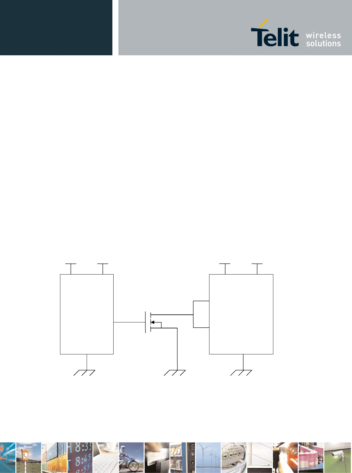
4.3.1 Reset
An active high host reset (RESET, ball D2), allowing the WE865-DUAL to be reset by an external
device (host).
This pin is internally pulled-down, do not drive the signal during normal operation.
The signal must be asserted for a period greater than 1ms.
VOLTAGE LEVELS @ 25 °C
Min [V] Max [V] Remark
VIH 2,0 3,0 -
Table 9
Figure 7
WE865-DUAL
RESET
WE865-DUAL HW User Guide
1vv0300787 Rev. 1 - 03/10/08
Reproduction forbidden without Telit Communications S.p.A. written authorization - All Rights Reserved page 22 of 48
4.3.2 Manual reset
An active low manual reset (MR_RESET*, ball C1), see the table below for the allowed voltage levels.
As the pin is internally pulled-up, do not drive the signal during normal operation.
The signal must be asserted for a period greater than 1ms.
VOLTAGE LEVELS @ 25 °C
Min [V] Max [V] Remark
VIL -0,3 0,825
Table 10
Figure 8
WE865-DUAL
MR_RESET*
WE865-DUAL HW User Guide
1vv0300787 Rev. 1 - 03/10/08
Reproduction forbidden without Telit Communications S.p.A. written authorization - All Rights Reserved page 23 of 48
4.4 SDIO signals
A 4-data bit SDIO interface is available on the WE865-DUAL that must be connected to the host
processor (Telit GE863-PRO3).
WE865-DUAL SDIO voltage levels are fully compatible with the GE863-PRO3 I/O voltage levels.
47 Ohm series resistor on each SDIO line and 12pF capacitor on clock line must be inserted in order
to avoid noise (see Electrical design guidelines chapter). Refer to §8.2.
Voltage levels for all the SDIO pins are reported in the table:
VOLTAGE LEVELS @ 25 °C
Min [V] Max [V] Remark
VIL -0,3 0,825
VIH 2,0625 3,6
VOL 0 0,125 I = 4mA
VOH 2,475 3,3 I = 4mA
Table 11

WE865-DUAL HW User Guide
1vv0300787 Rev. 1 - 03/10/08
Reproduction forbidden without Telit Communications S.p.A. written authorization - All Rights Reserved page 24 of 48
5 Thermal design guidelines
The thermal design for the power supply heat sink should be done taking into account the current
consumption involved in the appropriate power supply configuration. Please refer to §4.1.1.1 for
detailed information on the current consumption.

WE865-DUAL HW User Guide
1vv0300787 Rev. 1 - 03/10/08
Reproduction forbidden without Telit Communications S.p.A. written authorization - All Rights Reserved page 25 of 48
6 PCB layout design guidelines
In case of implementing the input power supply circuitry as described in the previous §4.2.2, the PCB
traces connecting the switching output to the inductor and the switching diode must be as short as
possible. It is recommended to place the inductor and the diode very close to the power switching IC.
This is done in order to reduce the radiated field (noise) of the switching frequency (100-500 kHz
usually).
The use of a good common ground plane is generally suggested.
The placement of the power supply on the board should be done in such a way to guarantee that the
high current return paths in the ground plane are not overlapped to any noise sensitive lines.
The power supply input cables should be kept separate from noise sensitive lines.
WE865-DUAL HW User Guide
1vv0300787 Rev. 1 - 03/10/08
Reproduction forbidden without Telit Communications S.p.A. written authorization - All Rights Reserved page 26 of 48
7 Antenna
The antenna connection and board layout design are the most important part in the full product design
and they strongly reflect on the product overall performances, hence read carefully and follow the
requirements and the guidelines for a proper design.
7.1 Wi-Fi antenna guidelines
General guidelines for an antenna and antenna line on PCB for a Telit WE865-DUAL device
ANTENNA REQUIREMENTS
Frequency range [MHz] 2400-2500
Gain [dBi] ≤ 2
Impedance [Ohm] 50
Maximum Input Power [mW] >100
VSWR recommended ≤2
Table 12
Frequency range indicated in order to support 14 Wi-Fi channels. Smaller ranges are allowed or
requested for application over 11 or 13 channels.
Please refer to IEEE specifications and to the proper regulatory body directives about 802.11
channels and antenna specifications in different countries.
When using the Telit WE865-DUAL, since there's no antenna connector on the module, the antenna
must be connected to the WE865-DUAL through the PCB with the antenna pad.
Please consider that antenna design and choice is dependent on the specific application.

WE865-DUAL HW User Guide
1vv0300787 Rev. 1 - 03/10/08
Reproduction forbidden without Telit Communications S.p.A. written authorization - All Rights Reserved page 27 of 48
This transmission line shall fulfill the following requirements:
ANTENNA LINE ON PCB REQUIREMENTS
Impedance [Ohm] 50
Maximum Attenuation [dB] 0.3
Coupling with other signals is not allowed
Table 13
7.2 Wi-Fi antenna PCB trace guidelines
• Ensure that the antenna line impedance is 50 ohm.
• Keep the antenna line on the PCB as short as possible in order to limit losses.
• Antenna line must have uniform characteristics, constant cross section, avoid meanders
and abrupt curves.
• Keep, if possible, one layer of the PCB used only for the Ground plane.
• Surround (on the sides, over and under) the antenna line on PCB with Ground, avoid
having other signal tracks facing directly the antenna line track.
• The ground around the antenna line on PCB has to be strictly connected to the Ground
Plane by placing vias once per 2mm at least.
• Place EM noisy devices as far as possible from WE865-DUAL antenna line.
• Keep the antenna line far away from the WE865-DUAL power supply lines.
• If you have EM noisy devices around the PCB hosting the WE865-DUAL, such as fast
switching ICs, take care of the shielding of the antenna line by burying it inside the layers
of PCB and surround it with Ground planes, or shield it with a metal frame cover.
• If you don't have EM noisy devices around the PCB of WE865-DUAL, by using a strip-line
on the superficial copper layer for the antenna line, the line attenuation will be lower than
a buried one.

WE865-DUAL HW User Guide
1vv0300787 Rev. 1 - 03/10/08
Reproduction forbidden without Telit Communications S.p.A. written authorization - All Rights Reserved page 28 of 48
7.3 Wi-Fi antenna installation guidelines
• Install the antenna in a place covered by the Wi-Fi signal.
• The antenna must be installed to provide a separation distance of at least 20 cm
from all persons and must not be co-located or operating in conjunction with any
other antenna or transmitter.
• Antenna shall not be installed inside metal cases.
• Antenna shall be installed also according Antenna manufacturer instructions.
WE865-DUAL HW User Guide
1vv0300787 Rev. 1 - 03/10/08
Reproduction forbidden without Telit Communications S.p.A. written authorization - All Rights Reserved page 29 of 48
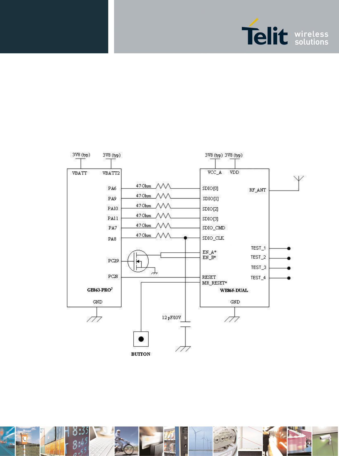
8 Integration with the GE863-PRO3
Figure 9 (Block diagram)
NOTE: It is mandatory to leave available the TEST lines in the customer design:
• TEST_1
• TEST_2
• TEST_3
• TEST_4
WE865-DUAL HW User Guide
1vv0300787 Rev. 1 - 03/10/08
Reproduction forbidden without Telit Communications S.p.A. written authorization - All Rights Reserved page 30 of 48
8.1 Power supply
When integrating the WE865-DUAL with the Telit GE863-PRO3 module, as described in previous
chapters a 3.8V (typ) voltage must be provided to the WE865-DUAL.
The WE865-DUAL power enable signals (EN_A* and EN_B*) must be connected together and be
driven by the GE863-PRO3 GPIO PC29 (ball F5) through a N-channel MOSFET.
In the GE863-PRO3 the power supply inputs of the GSM engine and the ARM processor part have
been kept separate, VBATT is the input for the GSM part, VBATT2 is the input for ARM.
It is possible to connect together the two power inputs since they have compatible ranges, but if it is
desired the two power supplies can be kept separate.
If keeping separated VBATT and VBATT2 is the chosen solution, the WE865-DUAL 3.8V power balls
(VCC_A) should be connected to the same voltage source feeding VBATT2.
Figure 10
WE865-DUAL
EN_B*
EN_A*
GE863-PRO3
PC29
3V8 (typ) 3V8 (typ)
VBATT VBATT2
3V8 (typ) 3V8 (typ)
GND GND
VCC_A VDD

WE865-DUAL HW User Guide
1vv0300787 Rev. 1 - 03/10/08
Reproduction forbidden without Telit Communications S.p.A. written authorization - All Rights Reserved page 31 of 48
8.2 SDIO signals
A 4-data bit SDIO interface is available on the WE865-DUAL that must be connected to the host
processor (Telit GE863-PRO3).
The WE865-DUAL SDIO voltage levels are fully compatible with the GE863-PRO3 I/O voltage levels.
47 Ohm series resistor on each SDIO line and 12pF capacitor on clock line must be inserted in order
to avoid noise (see Electrical design guidelines chapter). Refer to block diagram in Figure 7.
Figure 11

WE865-DUAL HW User Guide
1vv0300787 Rev. 1 - 03/10/08
Reproduction forbidden without Telit Communications S.p.A. written authorization - All Rights Reserved page 32 of 48
9 WE865-DUAL - Evaluation kit
The WE865-DUAL can be provided with an evaluation/testing kit.
The kit consists of:
• EVK-PRO3 evaluation kit for GE863-PRO3 module
(EVK-PRO3 main board + GE863-PRO3 interface board)
• WE865-DUAL interface board
In such a case, the WE865-DUAL module is directly soldered on its interface board. The figure below
shows how the boards must be assembled in order to allow the system working.
Figure 12
All the boards are connected each other via 40-pins connectors.
The core of the evaluation system is the EVK-PRO3 EVALUATION KIT, which can be split into several
functional blocks depending on the implemented function. Refer to the “EVK-PRO3 User Guide” for
additional information on the EVK-PRO3 description and usage.
EVK-PRO3 main board
GE863-PRO3 interface board
WE865-DUAL interface board
WE865-DUAL HW User Guide
1vv0300787 Rev. 1 - 03/10/08
Reproduction forbidden without Telit Communications S.p.A. written authorization - All Rights Reserved page 33 of 48
Figure 13
WE865-DUAL
interface board
WE865-DUAL
EVK-PRO3
GE863-PRO3
WE865-DUAL HW User Guide
1vv0300787 Rev. 1 - 03/10/08
Reproduction forbidden without Telit Communications S.p.A. written authorization - All Rights Reserved page 34 of 48
Figure 14
EVK-PRO3
WE865-DUAL
interface board
WE865-DUAL
GE863-PRO3

WE865-DUAL HW User Guide
1vv0300787 Rev. 1 - 03/10/08
Reproduction forbidden without Telit Communications S.p.A. written authorization - All Rights Reserved page 35 of 48
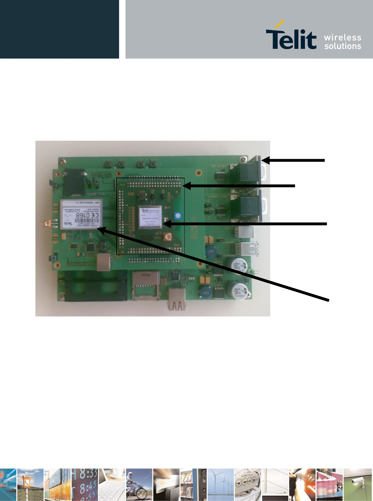
9.1 WE865-DUAL Interface board
9.1.1 Mechanical description
Figure 15
WE865-DUAL HW User Guide
1vv0300787 Rev. 1 - 03/10/08
Reproduction forbidden without Telit Communications S.p.A. written authorization - All Rights Reserved page 36 of 48
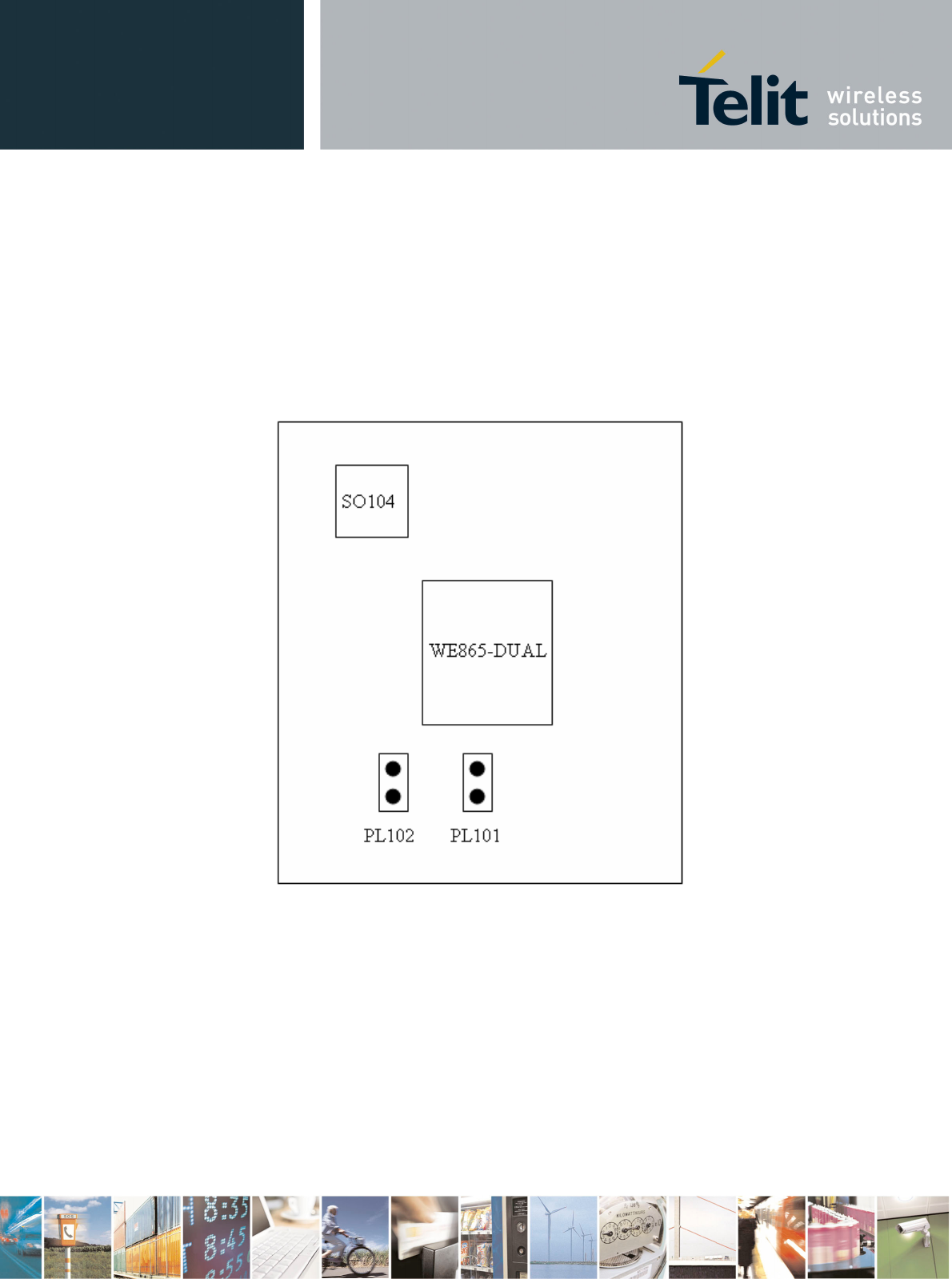
9.1.2 Main components
Main components TOP side list:
WE865-DUAL module
PL101: 2 pin jumper
PL102: 2 pin jumper
SW101: Reset button – Push to drive MR_RESET* low)
SO104: RF connector (alternative to AT101)
PL103: 5 pin header - SPI for test
Figure 16
WE865-DUAL HW User Guide
1vv0300787 Rev. 1 - 03/10/08
Reproduction forbidden without Telit Communications S.p.A. written authorization - All Rights Reserved page 37 of 48
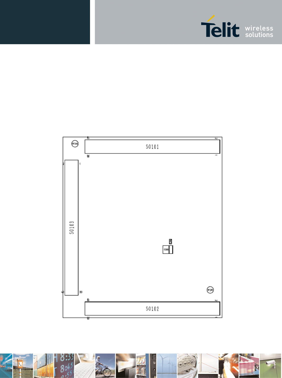
Main components BOTTOM side list:
SO101: Interface connector
SO102: Interface connector
SO103: Interface connector
Figure 17
WE865-DUAL HW User Guide
1vv0300787 Rev. 1 - 03/10/08
Reproduction forbidden without Telit Communications S.p.A. written authorization - All Rights Reserved page 38 of 48
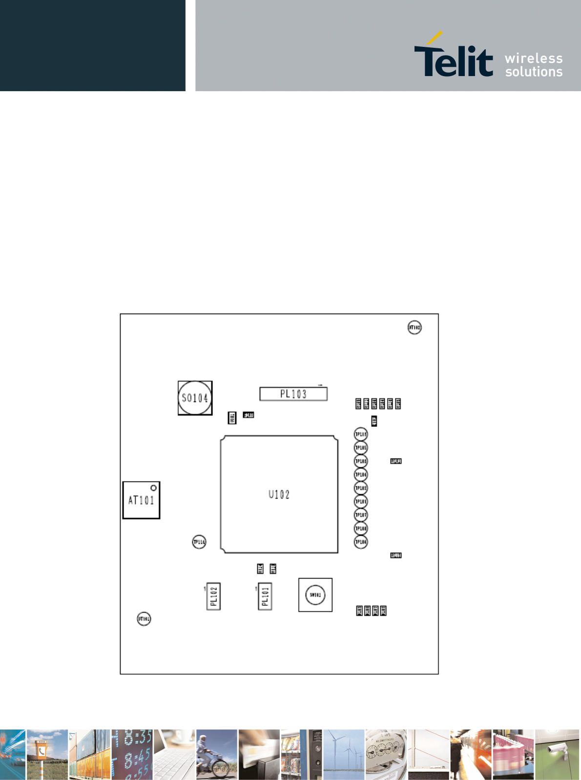
9.1.3 Jumpers settings
The figure below shows the PL101 and PL102 jumpers on the TOP side in the interface board
Figure 18
PL101 - Short the jumper to drive EN_A* low
PL102 - Short the jumper to drive EN_B* low
WE865-DUAL HW User Guide
1vv0300787 Rev. 1 - 03/10/08
Reproduction forbidden without Telit Communications S.p.A. written authorization - All Rights Reserved page 39 of 48
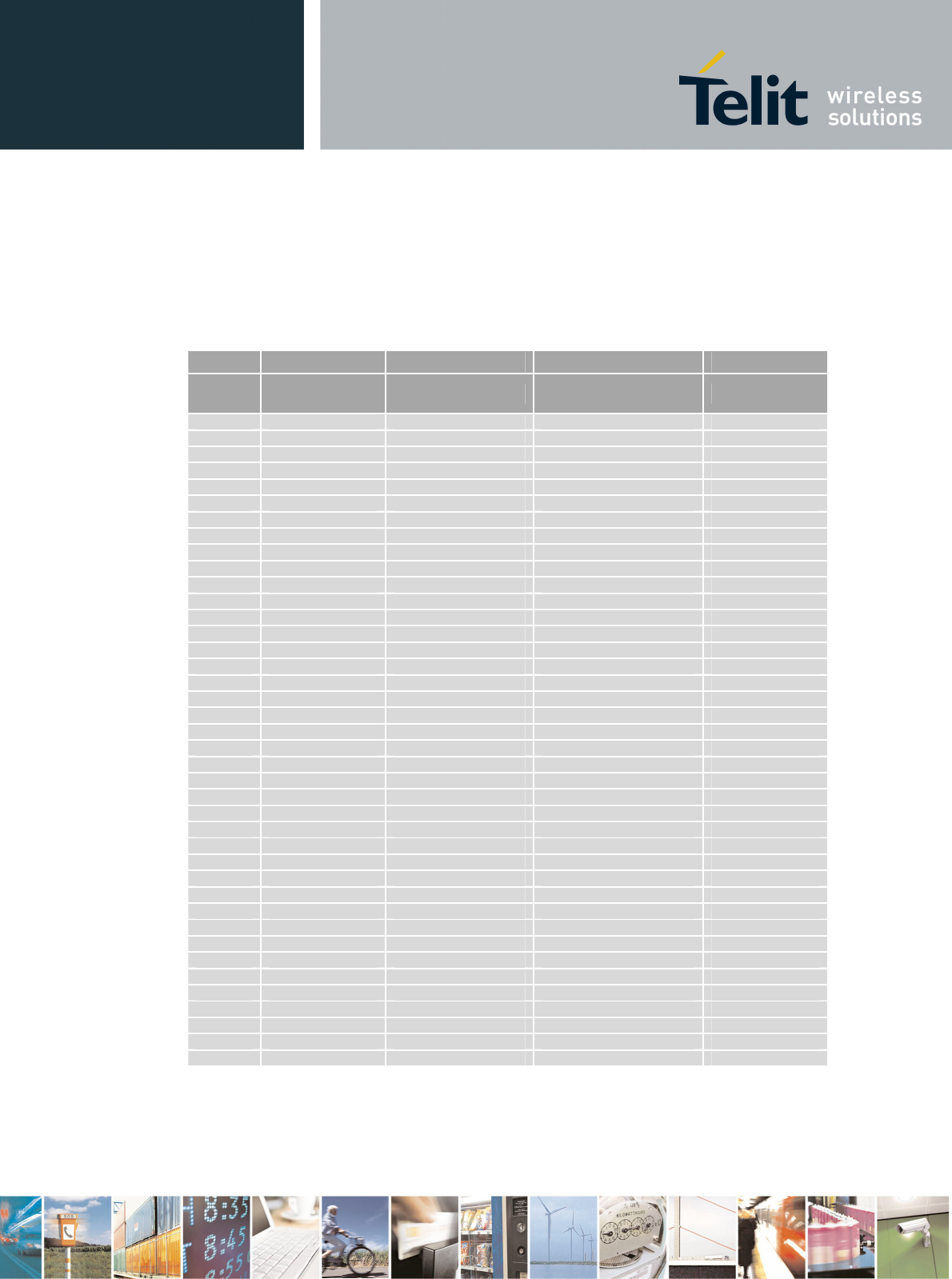
9.1.4 Pin table
SO101 SO102 SO103 PL103
Pin n. Signal name Signal name Signal name Signal name
1 RESERVED RESERVED RESERVED TEST_1
2 RESERVED RESERVED RESERVED TEST_2
3 RESERVED RESERVED RESERVED TEST_3
4 RESERVED RESERVED RESERVED TEST_4
5 RESERVED RESERVED RESERVED GND
6 RESERVED RESERVED RESERVED -
7 SDIO[0] RESERVED RESERVED -
8 SDIO_CMD RESERVED RESERVED -
9 SDIO_CLK RESERVED RESERVED -
10 SDIO[1] RESERVED RESERVED -
11 SDIO[2] RESERVED RESERVED -
12 SDIO[3] RESERVED RESERVED -
13 RESERVED RESERVED RESERVED -
14 RESERVED RESERVED RESERVED -
15 RESERVED RESERVED RESERVED -
16 RESERVED RESERVED RESERVED -
17 RESERVED RESERVED RESERVED -
18 RESERVED RESERVED RESERVED -
19 RESERVED RESERVED RESERVED -
20 RESERVED RESERVED RESERVED -
21 RESERVED RESERVED RESERVED -
22 RESERVED RESERVED RESERVED -
23 RESERVED RESERVED RESERVED -
24 RESERVED RESERVED RESERVED -
25 RESERVED RESERVED RESERVED -
26 RESERVED RESERVED RESERVED -
27 RESERVED RESERVED RESERVED -
28 RESERVED RESERVED RESERVED -
29 RESERVED RESERVED RESET -
30 RESERVED RESERVED RESERVED -
31 RESERVED RESERVED RESERVED -
32 RESERVED RESERVED RESERVED -
33 RESERVED RESERVED RESERVED -
34 RESERVED RESERVED RESERVED -
35 RESERVED RESERVED RESERVED -
36 VBATT RESERVED RESERVED -
37 RESERVED RESERVED GND -
38 RESERVED RESERVED RESERVED -
39 GND GND GND -
40 GND GND RESERVED -
Table 14
WE865-DUAL HW User Guide
1vv0300787 Rev. 1 - 03/10/08
Reproduction forbidden without Telit Communications S.p.A. written authorization - All Rights Reserved page 40 of 48
10 Mounting the WE865-DUAL on the
application board
The Telit WE865-DUAL module has been designed in order to be compliant with a standard lead-free
SMT process.
10.1 Stencil
Stencil’s apertures layout can be the same of the recommended footprint (1:1), we suggest a
thickness of stencil foil ≥ 120μm.
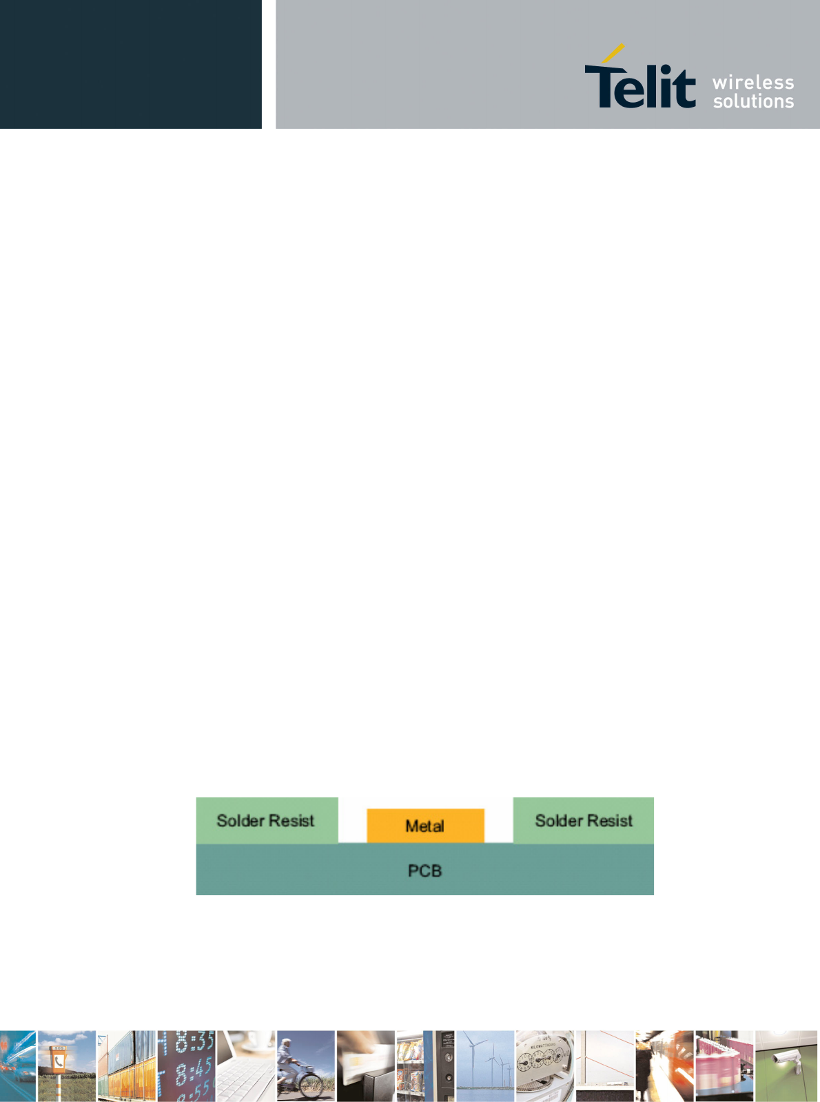
10.2 PCB pad design
"Non solder mask defined” (NSMD) type is recommended for the solder pads on the PCB.
Figure 19
WE865-DUAL HW User Guide
1vv0300787 Rev. 1 - 03/10/08
Reproduction forbidden without Telit Communications S.p.A. written authorization - All Rights Reserved page 41 of 48
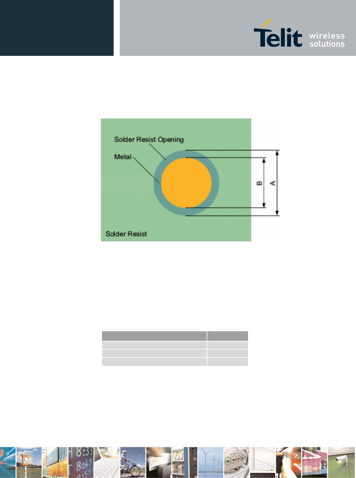
Figure 20
Recommendations for PCB pad dimensions
Dimension Value [mm]
Ball pitch 2
Solder resist opening diameter A 1,150
Metal PAD diameter B 1 +/- 0,05
Table 15
Placement of microvias not covered by solder resist is not recommended inside the “Solder resist
Opening”,unless the microvia carry the same signal of the pad itself.
WE865-DUAL HW User Guide
1vv0300787 Rev. 1 - 03/10/08
Reproduction forbidden without Telit Communications S.p.A. written authorization - All Rights Reserved page 42 of 48
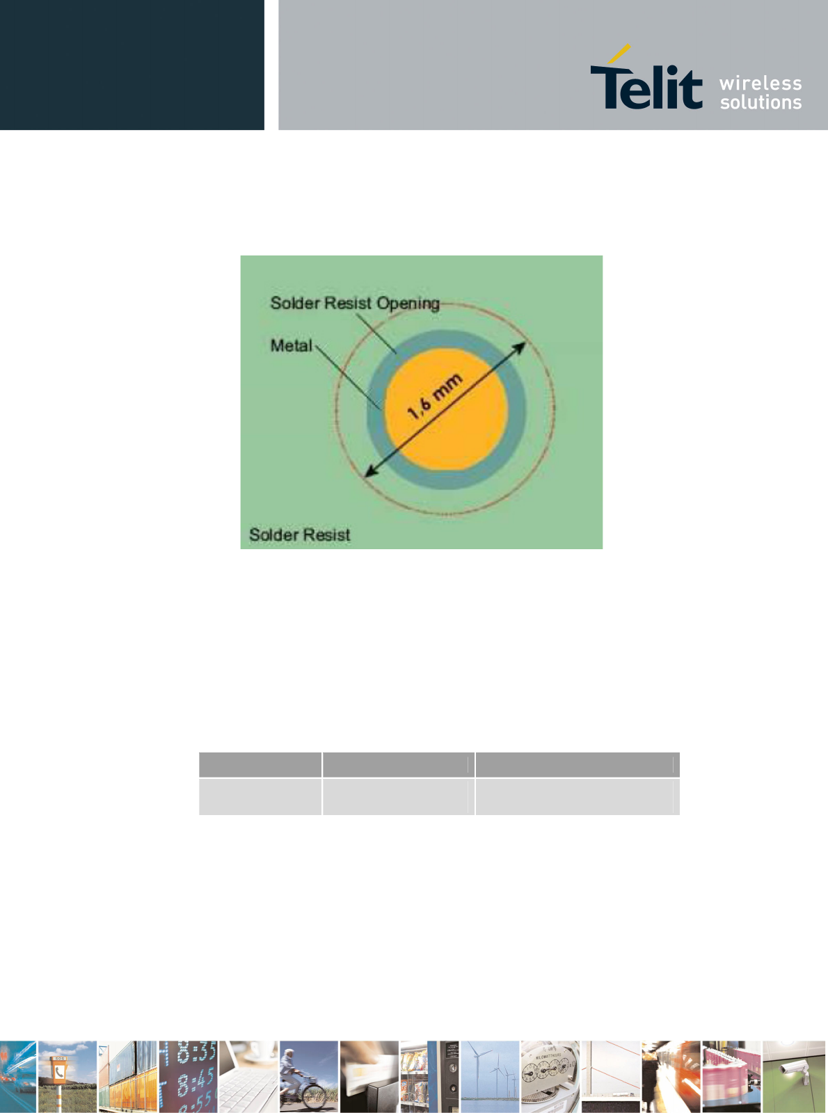
Figure 21
Holes in pad are allowed only for blind holes and not for through holes.
Recommendations for PCB pad surfaces:
Finish Layer tickness [um] Properties
Electro-less Ni /
Immersion Au
3-7 /
0,05-0,15
good solder ability protection,
high shear force values
Table 16
The PCB must be able to resist the higher temperatures, which are occurring at the lead-free process.
This issue should be discussed with the PCB-supplier. Generally, the wet-ability of tin-lead solder
paste on the described surface plating is better compared to lead-free solder paste.
WE865-DUAL HW User Guide
1vv0300787 Rev. 1 - 03/10/08
Reproduction forbidden without Telit Communications S.p.A. written authorization - All Rights Reserved page 43 of 48
10.3 Solder paste
Lead free
Solder paste Sn / Ag / Cu
Table 17
10.4 Solder reflow
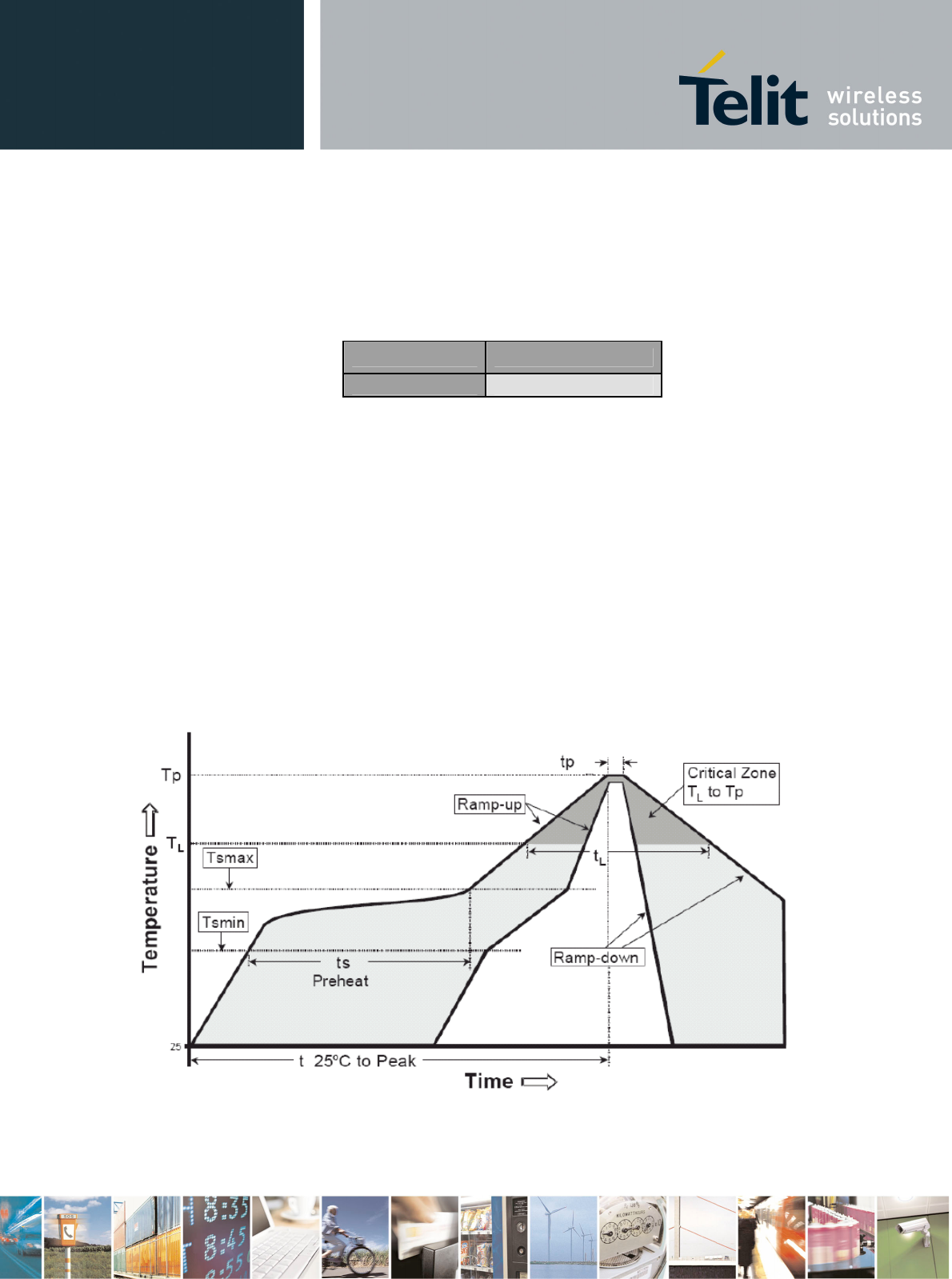
The following is the recommended solder reflow profile
Figure 22
WE865-DUAL HW User Guide
1vv0300787 Rev. 1 - 03/10/08
Reproduction forbidden without Telit Communications S.p.A. written authorization - All Rights Reserved page 44 of 48
Profile Feature Pb-Free
Assembly
Average ramp-up rate (TL to TP)
3 °C / second
max
Preheat:
- Temperature Min (Tsmin)
- Temperature Max (Tsmax)
- Time (min to max) (ts)
150 °C
200 °C
60-180
seconds
Tsmax to TL:
- Ramp-up rate
3 °C / second
max
Time maintaned above:
- Temperature (TL)
- Time (tL)
217 °C
60-150
seconds
Peak Temperature (Tp): 245 + 0/-5 °C
Time within 5 °C of actual Peak
Temperature (tp) 10-30 seconds
Ramp-down rate
6 °C/second
max
Time 25 °C to Peak Temperature 8 minutes max
Table 18
NOTE: All temperatures refer to topside of the package, measured on the package body surface.
IMPORTANT: WE865-DUAL module can accept only one reflow process

WE865-DUAL HW User Guide
1vv0300787 Rev. 1 - 03/10/08
Reproduction forbidden without Telit Communications S.p.A. written authorization - All Rights Reserved page 45 of 48
11 Moisture sensitivity
The level of moisture sensibility of Telit WE865-DUAL modules is “3”, according with standard
IPC/JEDEC J-STD-020, take care of all the relative requirements for using this kind of components.
Moreover, the customer has to take care of the following conditions:
• The shelf life of WE865 inside of the dry bag shall be 12 month from the bag seal date, when
stored in a non-condensing atmospheric environment of <40°C / 90% RH
• Environmental condition during the production: ≤ 30°C / 60% RH according to IPC/JEDEC J-
STD-033A paragraph 5
• The maximum time between the opening of the sealed bag and the reflow process shall be 168
• Hours if the condition b) “IPC/JEDEC J-STD-033A paragraph 5.2” is respected
• A baking is required if conditions b) or c) are not respected
• A baking is required if the humidity indicator inside the bag indicates 10% RH or more

WE865-DUAL HW User Guide
1vv0300787 Rev. 1 - 03/10/08
Reproduction forbidden without Telit Communications S.p.A. written authorization - All Rights Reserved page 46 of 48
12 Conformity assessment issues
Assessment of the final product must be made against the Essential requirements of the R&TTE
Directive Articles 3.1(a) and (b), safety and EMC respectively, and any relevant Article 3.3
requirements.
The WE865-DUAL module is conform with the following European Union Directives:
• R&TTE Directive 1999/5/EC (Radio Equipment & Telecommunications Terminal Equipments)
• Low Voltage Directive 73/23/EEC and product safety
• Directive 89/336/EEC for conformity for EMC
In order to satisfy the essential requisite of the R&TTE 99/5/EC directive, the WE865-DUAL module is
compliant with the following standards:
• Use of RF Spectrum. Standard: EN 300 328 v1.7.1 (2006-10)
• EMC (Electromagnetic Compatibility). Standards: EN 301 489-1 and EN 301 489-17
• LVD (Low Voltage Directive) Standards: EN 60 950
The WE865-DUAL module is conform with the following US Directives:
• Use of RF Spectrum. Standards: FCC 47 Part 15
• EMC (Electromagnetic Compatibility). Standards: FCC 47 Part 15
To meet the FCC's RF exposure rules and regulations:
- The system antenna(s) used for this transmitter must be installed to provide a separation
distance of at least 20 cm from all the persons and must not be co-located or operating in
conjunction with any other antenna or transmitter.
- The system antenna(s) used for this module must not exceed 2 dBi for all operating
configurations.
- Users and installers must be provided with antenna installation instructions and transmitter
operating conditions for satisfying RF exposure compliance.
Manufacturers of mobile, fixed or portable devices incorporating this module are advised to clarify
any regulatory questions and to have their complete product tested and approved for FCC
compliance.

WE865-DUAL HW User Guide
1vv0300787 Rev. 1 - 03/10/08
Reproduction forbidden without Telit Communications S.p.A. written authorization - All Rights Reserved page 47 of 48
13 Safety recommendations
READ CAREFULLY
Be sure the use of this product is allowed in the country and in the environment required. The use of
this product may be dangerous and has to be avoided in the following areas:
Where it can interfere with other electronic devices in environments such as hospitals, airports,
aircrafts, etc
Where there is risk of explosion such as gasoline stations, oil refineries, etc
It is responsibility of the user to enforce the country regulation and the specific environment regulation.
Do not disassemble the product; any mark of tampering will compromise the warranty validity.
We recommend following the instructions of the hardware user guides for a correct wiring of the
product. The product has to be supplied with a stabilized voltage source and the wiring has to be
conforming to the security and fire prevention regulations.
The product has to be handled with care, avoiding any contact with the pins because electrostatic
discharges may damage the product itself.
The system integrator is responsible of the functioning of the final product; therefore, care has to be
taken to the external components of the module, as well as of any project or installation issue,
because the risk of disturbing the external networks or devices or having impact on the security.
Should there be any doubt, please refer to the technical documentation and the regulations in force.
Every module has to be equipped with a proper antenna with specific characteristics. The antenna has
to be installed with care in order to avoid any interference with other electronic devices and has to
guarantee a minimum distance from the body (20 cm). In case of this requirement cannot be satisfied,
the system integrator has to assess the final product against the SAR regulation EN 50360.
The European Community provides some Directives for the electronic equipments introduced on the
market. All the relevant information’s are available on the European Community website:
http://europa.eu.int/comm/enterprise/rtte/dir99-5.htm
The text of the Directive 99/05 regarding telecommunication equipments is available, while the
applicable Directives (Low Voltage and EMC) are available at:
http://europa.eu.int/comm/enterprise/electr_equipment/index_en.htm
WE865-DUAL HW User Guide
1vv0300787 Rev. 1 - 03/10/08
Reproduction forbidden without Telit Communications S.p.A. written authorization - All Rights Reserved page 48 of 48
14 Document change log
R
Re
ev
vi
is
si
io
on
n
D
Da
at
te
e
C
Ch
ha
an
ng
ge
es
s
ISSUE#0 20/08/08 Preliminary Release
ISSUE#1 03/10/08 Updated mechanical dimensions
Updated pin-out and ball grid
Updated power configuration section
Added current consumption
Updated reset section
Updated antenna section
Updated integration section with GE863-PRO3
Updated evaluation kit section
Added conformity assessment issues section
Added safety recommendations section