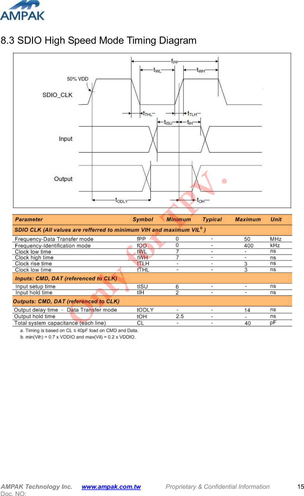
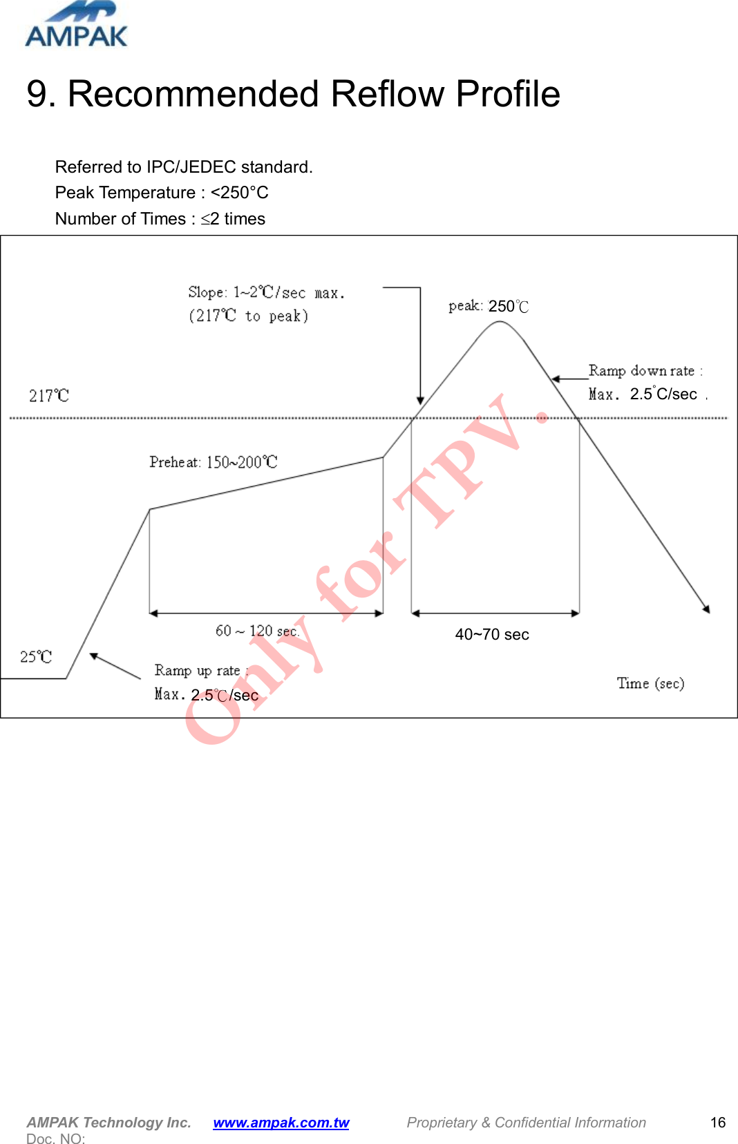
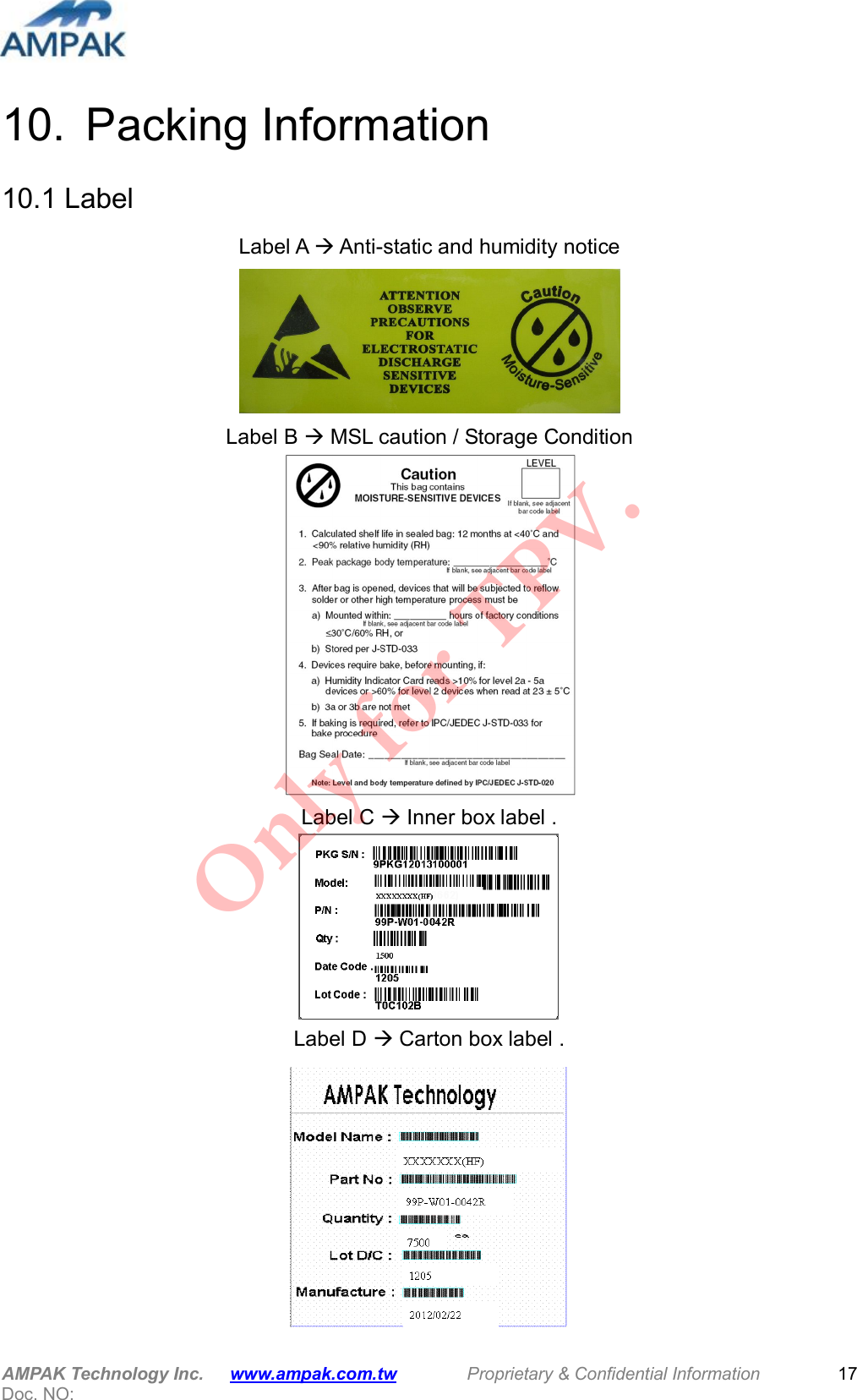
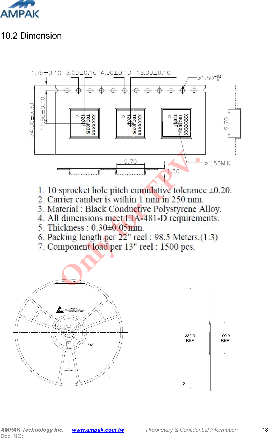
Top Victory Electronics WL211 Wi-Fi SIP Module User Manual rev

Top Victory Electronics (Taiwan) Co Ltd Wi-Fi SIP Module rev

User Manual rev.pdf

 AMPAK Technology Inc.      www.ampak.com.tw        Proprietary & Confidential Information   Doc. NO:      正基科技股份有限公司  SPECIFICATION  SPEC. NO.:  REV:        1.9  DATE:   07.20. 2012  PRODUCT    NAME:  WL-211              APPROVED  CHECKED  PREPARED  DCC ISSUE NAME         Only for TPV.
 AMPAK Technology Inc.      www.ampak.com.tw        Proprietary & Confidential Information   Doc. NO:      AMPAK   WL-211 Wi-Fi SIP Module Spec Sheet       Only for TPV.
 AMPAK Technology Inc.      www.ampak.com.tw          Proprietary & Confidential Information   Doc. NO:                                                             1 Revision History                       Date  Revision Content  Revised By Version 2011/08/22  -Initial released    Andy  1.0 2011/09/27  -Modify physical dimensions  Andy  1.1 2011/10/19  -Modify block diagram  Andy  1.2 2011/12/23  -Add Power Consumption  Andy  1.3 2012/01/12  -Modify dimension  Andy  1.4 2012/03/09  -Add packing information  Andy  1.5 2012/03/19  -More info to recommended footprint  Andy  1.6 2012/05/03  -Pin description revised  Bart  1.7 2012/05/18  -Modify Recommended Footprint -Modify Physical Dimensions  Bart  1.8 2012/07/20  -Modify Physical Dimensions  Bart  1.9        Only for TPV.
 AMPAK Technology Inc.      www.ampak.com.tw        Proprietary & Confidential Information       Doc. NO:   2 Contents Revision History......................................................................................................... 1 Contents..................................................................................................................... 2 1. Introduction........................................................................................................... 3 2. Features ............................................................................................................... 4 3. Deliverables.......................................................................................................... 5 3.1 Deliverables.................................................................................................... 5 3.2 Regulatory certifications ................................................................................. 5 4. General Specification............................................................................................ 6 4.1 Wi-Fi RF Specification .................................................................................... 6 4.2 Voltages.......................................................................................................... 7 4.2.1 Absolute Maximum Ratings.................................................................... 7 4.2.2 Recommended Operating Ratings ......................................................... 7 5. Pin Assignments ................................................................................................... 8 5.1 PCB Pin Outline.............................................................................................. 8 5.2 Pin Definition .................................................................................................. 8 6. Dimensions......................................................................................................... 11 6.1 Physical Dimensions..................................................................................... 11 6.2 Recommended Footprint .............................................................................. 12 7. External clock reference ..................................................................................... 13 7.1 SDIO Pin Description.................................................................................... 13 8. Host Interface Timing Diagram ........................................................................... 14 8.1 Power-up Sequence Timing Diagram ........................................................... 14 8.2 SDIO Default Mode Timing Diagram............................................................. 14 8.3 SDIO High Speed Mode Timing Diagram ..................................................... 15 9. Recommended Reflow Profile ............................................................................ 16 10. Packing Information............................................................................................ 17 10.1 Label........................................................................................................... 17 10.2 Dimension................................................................................................... 18 10.3 MSL Level / Storage Condition ................................................................... 20         Only for TPV.
 AMPAK Technology Inc.      www.ampak.com.tw        Proprietary & Confidential Information       Doc. NO:   3 1. Introduction AMPAK Technology would like to announce a low-cost and low-power consumption module which has all of the Wi-Fi functionalities. The highly integrated WL-211 module makes the possibilities of web browsing, VoIP, headsets and other applications. With seamless roaming capabilities  and  advanced  security,  WL-211  can  also  interact  with  different  vendors’ 802.11b/g/n Access Points in the wireless LAN.  This wireless module complies with IEEE 802.11 b/g/n standard and it can achieve up to a speed  of  72.2Mbps  with  single  stream  in  802.11n  draft,  54Mbps  as  specified  in  IEEE 802.11g,  or  11Mbps  for  IEEE  802.11b  to  connect  to  the  wireless  LAN.  The  integrated module provides SDIO interface for Wi-Fi.  This compact  module is  a  total solution for Wi-Fi technologies. The module is specifically developed for Smart phones and Portable devices.           Only for TPV.
 AMPAK Technology Inc.      www.ampak.com.tw        Proprietary & Confidential Information       Doc. NO:   4 2. Features   Single-band 2.4GHz IEEE 802.11b/g/n   Supports standard interfaces SDIO v2.0(50MHz, 4-bit and 1-bit) and generic SPI(up to 50MHz)   Integrated ARM Cortex-M3TM CPU with on-chip memory enables running IEEE802.11 firmware that can be field-upgraded with future features.   Supports per packet Rx antenna diversity   Security: i.  Hardware WAPI acceleration engine ii.  AES  and  TKIP  in  hardware  for  faster  data  encryption  and  IEEE  802.11i compatibility iii.  WPATM  –  and  WPA2TM  -  (Personal)  support  for  powerful  encryption  and authentication   A simplified block diagram of the module is depicted in the figure below.      Only for TPV.
 AMPAK Technology Inc.      www.ampak.com.tw        Proprietary & Confidential Information       Doc. NO:   5 3. Deliverables   3.1 Deliverables The following products and software will be part of the product.   Module with packaging   Evaluation Kits   Software utility for integration, performance test.   Product Datasheet.   Agency certified pre-tested report with the adapter board. 3.2 Regulatory certifications The product delivery is a pre-tested module, without the module level certification. For module approval, the platform’s antennas are required for the certification. Only for TPV.
 AMPAK Technology Inc.      www.ampak.com.tw        Proprietary & Confidential Information       Doc. NO:   6 4. General Specification 4.1 Wi-Fi RF Specification Conditions : VBAT=3.6V ; VDDIO=3.3V ; Temp:25°C Feature  Description Product Name  WL-211 Wi-Fi SIP Module WLAN Standard  IEEE 802.11b/g/n, WiFi compliant Host Interface  SDIO Dimension  L x W x H: 9.5 x 9.5 x 1.5 (typical) mm Frequency Range    2.412 GHz ~ 2.4835 GHz (2.4 GHz ISM Band) Number of Channels  11 for North America, 13 for Europe, and 14 for Japan Modulation  802.11b : DQPSK, DBPSK, CCK 802.11g/n : OFDM /64-QAM,16-QAM, QPSK, BPSK   802.11b /11Mbps : 16 dBm ± 1.5 dB @ EVM  -9dB 802.11g /54Mbps : 15 dBm ± 1.5 dB @ EVM  -25dB Output Power 802.11n /65Mbps : 14 dBm ± 1.5 dB @ EVM  -28dB -    MCS=0    PER @ -85 ± 1dBm, typical -    MCS=1      PER @ -84 ± 1dBm, typical -    MCS=2    PER @ -82 ± 1dBm, typical -    MCS=3    PER @ -80 ± 1dBm, typical -    MCS=4    PER @ -77 ± 1dBm, typical -    MCS=5    PER @ -73 ± 1dBm, typical -    MCS=6    PER @ -71 ± 1dBm, typical Receive Sensitivity (11n,20MHz)   @10% PER -    MCS=7      PER @ -69 ± 1dBm, typical -      6Mbps    PER @ -87 ± 1dBm, typical -      9Mbps     PER @ -86 ± 1dBm, typical -    12Mbps    PER @ -85 ± 1dBm, typical -    18Mbps    PER @ -83 ± 1dBm, typical -    24Mbps    PER @ -81 ± 1dBm, typical -    36Mbps    PER @ -78 ± 1dBm, typical -    48Mbps    PER @ -74 ± 1dBm, typical Receive Sensitivity (11g) @10% PER -    54Mbps    PER @ -72 ± 1dBm, typical -    1Mbps      PER @ -90 ± 1dBm, typical -    2Mbps    PER @ -89 ± 1dBm, typical -    5.5Mbps   PER @ -87 ± 1dBm, typical Receive Sensitivity (11b) @8% PER -    11Mbps    PER @ -84 ± 1dBm, typical Only for TPV.
 AMPAK Technology Inc.      www.ampak.com.tw        Proprietary & Confidential Information       Doc. NO:   7 802.11b : 1, 2, 5.5, 11Mbps Data Rate 802.11g : 6, 9, 12, 18, 24, 36, 48, 54Mbps Data Rate (20MHz ,Long GI,800ns) 802.11n: 6.5, 13, 19.5, 26, 39, 52, 58.5, 65Mbps Data Rate (20MHz ,short GI,400ns) 802.11n : 7.2, 14.4, 21.7, 28.9, 43.3, 57.8, 65,72.2Mbps 802.11b : -10 dBm Maximum Input Level  802.11g/n : -20 dBm Operating temperature  -30°C to 85°C Storage temperature  -40°C to 85°C Humidity  Operating Humidity 10% to 95% Non-Condensing Storage Humidity 5% to 95% Non-Condensing   4.2 Voltages 4.2.1 Absolute Maximum Ratings Symbol  Description  Min. Max. Unit VBAT  Input supply Voltage  -0.5 6.5  V VDDIO  Digital/Bluetooth/SDIO/SPI I/O Voltage  -0.5 4.1  V  4.2.2 Recommended Operating Ratings Test conditions: At room temperature 25°C   Symbol  Min.  Typ.  Max.  Unit VBAT  3.0  3.6  4.8  V 1.7  1.8  1.92  V VDDIO  2.97  3.3  3.6  V Note: The voltage of VDDIO is depended on system I/O voltage.  Test conditions: At operating temperature -10°C ~65°C Symbol  Min.  Typ.  Max.  Unit VBAT  3.0  3.6  4.8  V VDDIO  1.7  -  3.35  V Note: VDDIO operating voltage range from 1.7V to 3.35V at operating temperature is guaranteed.  Only for TPV.
 AMPAK Technology Inc.      www.ampak.com.tw        Proprietary & Confidential Information       Doc. NO:   8 5. Pin Assignments 5.1 PCB Pin Outline  < TOP VIEW > 5.2 Pin Definition NO Name Type Description 1 WLAN_ANT I/O RF signal I/O port 2 GND  -  Ground 3 JTAG_TRST_L  I JTAG interface, if JTAG not used unconnected (NC) 4 JTAG_TDO_UART_TX O JTAG interface, if JTAG not used unconnected (NC) this pin. This pin is also muxed with UART_TX, which can be enabled by software 5 JTAG_TDI_UART_RX I JTAG interface, if JTAG not used unconnected (NC) this pin. This pin is also muxed with UART_RX, which can be enabled by software 6 JTAG_TCK  I JTAG interface, if JTAG not used unconnected (NC) 7 JTAG_TMS  I JTAG interface, if JTAG not used unconnected (NC) 8 GND  -  Ground 9 OSC_IN  I XTAL oscillator input 10 OSC_OUT  I/O XTAL oscillator output 11 GND  -  Ground 12 RF_SW_CTRL0  -  Floating (Don’t connected to ground) 13 RF_SW_CTRL3  -  Floating (Don’t connected to ground) Only for TPV.
 AMPAK Technology Inc.      www.ampak.com.tw        Proprietary & Confidential Information       Doc. NO:   9 14 GND  -  Ground 15 GND  -  Ground 16 GND  -  Ground 17 GND  -  Ground 18 VIO I Digital I/O Voltage input 19 CLK_32K  I Sleep clock (32.768KHz) input 20 SDIO_DATA_2  I/O SDIO data line 2 21 SDIO_DATA_0  I/O SDIO data line 0 22 SDIO_CLK  I SDIO clock 23 SDIO_CMD  I/O SDIO command line 24 SDIO_DATA_1  I/O SDIO data line 1 25 SDIO_DATA_3  I/O SDIO data line 3 26 VIN_LDO  I Internal DC-DC regulator input 27 GND  -  Ground 28 SR_VLX  O   Internal DC-DC regulator output 29 GND  -  Ground 30 VBAT I DC voltage input 31 WL_RST_N  I Active low WLAN reset signal 32 GND  -  Ground 33 GND  -  Ground 34 GND  -  Ground 35 GND  -  Ground 36 XTAL_PU  O Floating (Don’t connected to ground) 37 GND  -  Ground 38 GND  -  Ground 39 GND  -  Ground 40 GND  -  Ground 41 GND  -  Ground 42 GND  -  Ground 43 VDD_TCXO  -  Floating (Don’t connected to ground) 44 GND  -  Ground 45 TCXO_IN  -  Floating (Don’t connected to ground) 46 GPIO_5  -  Floating (Don’t connected to ground) 47 GPIO_4  -  Floating (Don’t connected to ground) 48 GPIO_3  -  Floating (Don’t connected to ground) 49 GPIO_1  O  WL_Host Wake,   50 GPIO_0  -  Mode selection, Low for SDIO, High for SPI mode 51 WRF_GPIO_OUT  -  Floating (Don’t connected to ground) Only for TPV.
 AMPAK Technology Inc.      www.ampak.com.tw        Proprietary & Confidential Information       Doc. NO:   10 52 GND  -  Ground 53 GND  -  Ground 54 GND  - Ground 55 GND  - Ground 56 GND  - Ground 57 GND  - Ground 58 GND  - Ground 59 GND  - Ground 60 GND  - Ground 61 GND -  Ground                             Only for TPV.
 AMPAK Technology Inc.      www.ampak.com.tw        Proprietary & Confidential Information       Doc. NO:   11 6. Dimensions 6.1 Physical Dimensions (Unit: mm)                       < TOP VIEW >                          < Side View >            < TOP VIEW >  1.7 (MAX)Only for TPV.
 AMPAK Technology Inc.      www.ampak.com.tw        Proprietary & Confidential Information       Doc. NO:   12 6.2 Recommended Footprint (Unit: mm)                           < TOP VIEW >               Only for TPV.
 AMPAK Technology Inc.      www.ampak.com.tw        Proprietary & Confidential Information       Doc. NO:   13 7. External clock reference External LPO signal characteristics Parameter  LPO Clock  Units Nominal input frequency  32.768  kHz Frequency accuracy  30 ppm Duty cycle  30 - 70  % Input signal amplitude  1600 to 3300 mV, p-p Signal type  Square-wave or sine-wave - Input impedance        >100k <5    pF Clock jitter (integrated over 300Hz – 15KHz)  <1  Hz  7.1 SDIO Pin Description The WL-211 supports SDIO version 1.2 for both 1-bit (25 Mbps), 4-bit modes (100 Mbps), and high speed 4-bit (50 MHz clocks – 200 Mbps). It has the ability to stop the SDIO clock and map the interrupt signal into a GPIO pin. This ‘out-of-band’ interrupt signal notifies the host when the WLAN device  wants to turn on the SDIO interface. The ability to force the control of the gated clocks from within the WLAN chip is also provided. ※  Function 0 Standard SDIO function (Max BlockSize / ByteCount = 32B) ※  Function  1  Backplane  Function  to  access  the  internal  System  On  Chip  (SOC) address space (Max BlockSize / ByteCount = 64B) ※  Function 2 WLAN Function for efficient WLAN packet transfer through DMA (Max BlockSize / ByteCount = 512B)  SDIO Pin Description SD 4-Bit Mode  SD 1-Bit Mode  SPI Mode DATA0 Data Line 0  DATA Data Line  DO  Data Output DATA1 Data Line 1 or Interrupt  IRQ  Interrupt  IRQ  Interrupt DATA2 Data Line 2 or Read Wait  RW  Read Wait  NC  Not Used DATA3 Data Line 3  NC  Not Used  CS  Card Select CLK  Clock  CLK  Clock  SCLK Clock CMD  Command Line  CMD  Command Line  DI  Data Input Only for TPV.
 AMPAK Technology Inc.      www.ampak.com.tw        Proprietary & Confidential Information       Doc. NO:   14 8.   Host Interface Timing Diagram 8.1 Power-up Sequence Timing Diagram  ※  WL_RST_N: Low asserting Reset for WLAN Core. This pin must be driven high or low (not left floating). 8.2 SDIO Default Mode Timing Diagram   Only for TPV.
 AMPAK Technology Inc.      www.ampak.com.tw        Proprietary & Confidential Information       Doc. NO:   15 8.3 SDIO High Speed Mode Timing Diagram        Only for TPV.
 AMPAK Technology Inc.      www.ampak.com.tw        Proprietary & Confidential Information       Doc. NO:   16 9. Recommended Reflow Profile  Referred to IPC/JEDEC standard. Peak Temperature : <250°C Number of Times : 2 times   10   2.5 /sec℃ 2.5°C/sec 40~70 sec 250℃ Only for TPV.
 AMPAK Technology Inc.      www.ampak.com.tw        Proprietary & Confidential Information       Doc. NO:   17 10.  Packing Information 10.1 Label Label A  Anti-static and humidity notice  Label B  MSL caution / Storage Condition  Label C  Inner box label .  Label D  Carton box label .  Only for TPV.
 AMPAK Technology Inc.      www.ampak.com.tw        Proprietary & Confidential Information       Doc. NO:   18 10.2 Dimension                          Only for TPV.
 AMPAK Technology Inc.      www.ampak.com.tw        Proprietary & Confidential Information       Doc. NO:   19                               A B C Humidity indicator Desiccant C D Only for TPV.
 AMPAK Technology Inc.      www.ampak.com.tw        Proprietary & Confidential Information       Doc. NO:   20 10.3 MSL Level / Storage Condition   ※NOTE : Accumulated baking time should not exceed 96hrs    Only for TPV.
  FThis dethe folinterferincludin This eqClass Bare desiresidentfrequeninstructHoweveinstallattelevisioand on,followin - Reor- Incre- Connto wh- Cons FCC Cparty reequipm This traother an   Federal Coevice complllowing twrence, and ng interferequipment haB digital deigned to protial installancy energy tions, may er, there is tion.  If thon receptio, the user isng measurerient or relocease the sepnect the equhich the recsult the dealaution: Anyesponsible fment. ansmitter mntenna or tra ommunicatilies with Pao condition(2) this dnce that maas been tesvice, pursuovide reasontion. This eand, if nocause hano guarantehis equipmeon, which cs encouragees: cate the recaration betwuipment intoeiver is conler or an expy changes ofor complianmust not be ansmitter.ion Commart 15 of thns: (1) Thdevice musay cause undsted and fouant to Part nable protecequipment ot installedarmful inteee that interent does cacan be detered to try to eiving antenween the eqo an outlet onnected. perienced raor modificance could vco-located  ission Interhe FCC Rulhis device st accept adesired operound to com15 of the Fction againsgenerates, ud and usederference torference wiause harmfurmined by correct the nna. quipment anon a circuit dadio/TV tecations not evoid the useor operatinrference Stes. Operatiomay not any interferration. mply with tFCC Rulesst harmful iuses and cad in accordo radio coill not occurul interferenturning theinterferencd receiver. different frochnician for expressly apr's authorityng in conjuntatement on is subjecause harmrence receithe limits f.  These liinterferencean radiate rdance withommunicatir in a particnce to radie equipmence by one ofom that r help. pproved byy to operatenction with21 ct to mful ived, for a imits e in a radio the ions.  cular io or t off f the y the e this h any
This devic1) Theante2) Theor aAs longrequiredend-promoduleIMPORexamplthen thenot be uwill be and obtEnd ProFOR MThis tramay be users. Tfollowinused once is intendede antenna menna and use transmitterantenna. g as 2 condid. Howeveroduct for ane installed RTANT NOe certain lape FCC authoused on the responsibletaining a sepoduct LabeMOBILE Dansmitter moinstalled suThe final endng: “Containly when alld only for Omust be instaers, and r module mtions abover, the OEM ny additionaOTE: In theptop configorization is final produe for re-evalparate FCC ling  EVICE USodule is autuch that 20 d product mins FCC IDl FCC compOEM integraalled such thmay not be coe are met, fuintegrator ial compliance event that gurations or no longer cuct. In these luating the authorizatiSAGE (>20thorized onlcm may be must be labe:ARS-WL211 pliance requators under hat 20 cm iso-located wurther transms still respoce requiremthese condico-locationconsidered vcircumstanend producon. 0cm/low powly for use inmaintainedeled in a vis”. Theuirements arthe followin maintainedwith any othemitter test wnsible for tements requireitions can nn with anothvalid and thnces, the OEt (includingwer) n device whd between thible area wi grantee's  re met. ng conditiond between ther transmittwill not be esting their ed with thisnot be met (fher transmitthe FCC ID cEM integratog the transmhere the antehe antenna aith the FCC ID can22 ns: he ter  for ter), can or mitter) enna and  be Manuaal Informattion To the End UserThe OEEM integratregardinng how to iend prooduct whicThe enddas showwoor has to bnnstall or rehh integrates  user manuual shall in in this mannual. ee aware not to provide mmove this RRF module itthis modulee. cclude all reqquired reguliinformationn to the end nn the user’ss manual of atory informmuser the ation/warnning

Navigation menu