Top Victory Electronics WL211 Wi-Fi SIP Module User Manual rev
Top Victory Electronics (Taiwan) Co Ltd Wi-Fi SIP Module rev
User Manual rev.pdf

AMPAK Technology Inc. www.ampak.com.tw Proprietary & Confidential Information
Doc. NO:
正基科技股份有限公司
SPECIFICATION
SPEC. NO.: REV: 1.9
DATE: 07.20. 2012
PRODUCT NAME: WL-211
APPROVED CHECKED PREPARED DCC ISSUE
NAME
Only for TPV.
AMPAK Technology Inc. www.ampak.com.tw Proprietary & Confidential Information
Doc. NO:
AMPAK
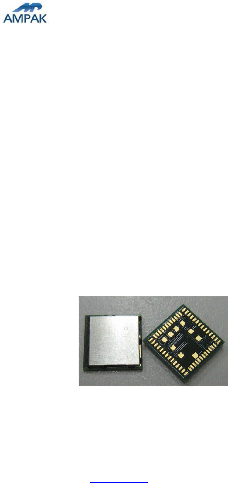
WL-211
Wi-Fi SIP Module
Spec Sheet
Only for TPV.

AMPAK Technology Inc. www.ampak.com.tw Proprietary & Confidential Information
Doc. NO:
1
Revision History
Date Revision Content Revised By
Version
2011/08/22 -Initial released Andy 1.0
2011/09/27 -Modify physical dimensions Andy 1.1
2011/10/19 -Modify block diagram Andy 1.2
2011/12/23 -Add Power Consumption Andy 1.3
2012/01/12 -Modify dimension Andy 1.4
2012/03/09 -Add packing information Andy 1.5
2012/03/19 -More info to recommended footprint Andy 1.6
2012/05/03 -Pin description revised Bart 1.7
2012/05/18 -Modify Recommended Footprint
-Modify Physical Dimensions Bart 1.8
2012/07/20 -Modify Physical Dimensions Bart 1.9
Only for TPV.

AMPAK Technology Inc. www.ampak.com.tw Proprietary & Confidential Information
Doc. NO:
2
Contents
Revision History......................................................................................................... 1
Contents..................................................................................................................... 2
1. Introduction........................................................................................................... 3
2. Features ............................................................................................................... 4
3. Deliverables.......................................................................................................... 5
3.1 Deliverables.................................................................................................... 5
3.2 Regulatory certifications ................................................................................. 5
4. General Specification............................................................................................ 6
4.1 Wi-Fi RF Specification .................................................................................... 6
4.2 Voltages.......................................................................................................... 7
4.2.1 Absolute Maximum Ratings.................................................................... 7
4.2.2 Recommended Operating Ratings ......................................................... 7
5. Pin Assignments ................................................................................................... 8
5.1 PCB Pin Outline.............................................................................................. 8
5.2 Pin Definition .................................................................................................. 8
6. Dimensions......................................................................................................... 11
6.1 Physical Dimensions..................................................................................... 11
6.2 Recommended Footprint .............................................................................. 12
7. External clock reference ..................................................................................... 13
7.1 SDIO Pin Description.................................................................................... 13
8. Host Interface Timing Diagram ........................................................................... 14
8.1 Power-up Sequence Timing Diagram ........................................................... 14
8.2 SDIO Default Mode Timing Diagram............................................................. 14
8.3 SDIO High Speed Mode Timing Diagram ..................................................... 15
9. Recommended Reflow Profile ............................................................................ 16
10. Packing Information............................................................................................ 17
10.1 Label........................................................................................................... 17
10.2 Dimension................................................................................................... 18
10.3 MSL Level / Storage Condition ................................................................... 20
Only for TPV.

AMPAK Technology Inc. www.ampak.com.tw Proprietary & Confidential Information
Doc. NO:
3
1. Introduction
AMPAK Technology would like to announce a low-cost and low-power consumption module
which has all of the Wi-Fi functionalities. The highly integrated WL-211 module makes the
possibilities of web browsing, VoIP, headsets and other applications. With seamless roaming
capabilities and advanced security, WL-211 can also interact with different vendors’
802.11b/g/n Access Points in the wireless LAN.
This wireless module complies with IEEE 802.11 b/g/n standard and it can achieve up to a
speed of 72.2Mbps with single stream in 802.11n draft, 54Mbps as specified in IEEE
802.11g, or 11Mbps for IEEE 802.11b to connect to the wireless LAN. The integrated
module provides SDIO interface for Wi-Fi.
This compact module is a total solution for Wi-Fi technologies. The module is specifically
developed for Smart phones and Portable devices.
Only for TPV.
AMPAK Technology Inc. www.ampak.com.tw Proprietary & Confidential Information
Doc. NO:
4
2. Features
Single-band 2.4GHz IEEE 802.11b/g/n
Supports standard interfaces SDIO v2.0(50MHz, 4-bit and 1-bit) and generic SPI(up to
50MHz)
Integrated ARM Cortex-M3TM CPU with on-chip memory enables running IEEE802.11
firmware that can be field-upgraded with future features.
Supports per packet Rx antenna diversity
Security:
i. Hardware WAPI acceleration engine
ii. AES and TKIP in hardware for faster data encryption and IEEE 802.11i
compatibility
iii. WPATM – and WPA2TM - (Personal) support for powerful encryption and
authentication
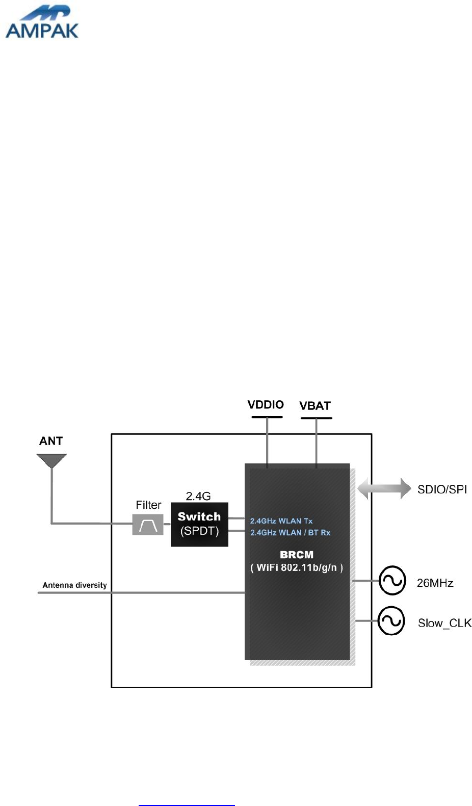
A simplified block diagram of the module is depicted in the figure below.
Only for TPV.

AMPAK Technology Inc. www.ampak.com.tw Proprietary & Confidential Information
Doc. NO:
5
3. Deliverables
3.1 Deliverables
The following products and software will be part of the product.
Module with packaging
Evaluation Kits
Software utility for integration, performance test.
Product Datasheet.
Agency certified pre-tested report with the adapter board.
3.2 Regulatory certifications
The product delivery is a pre-tested module, without the module level certification. For
module approval, the platform’s antennas are required for the certification.
Only for TPV.
AMPAK Technology Inc. www.ampak.com.tw Proprietary & Confidential Information
Doc. NO:
6
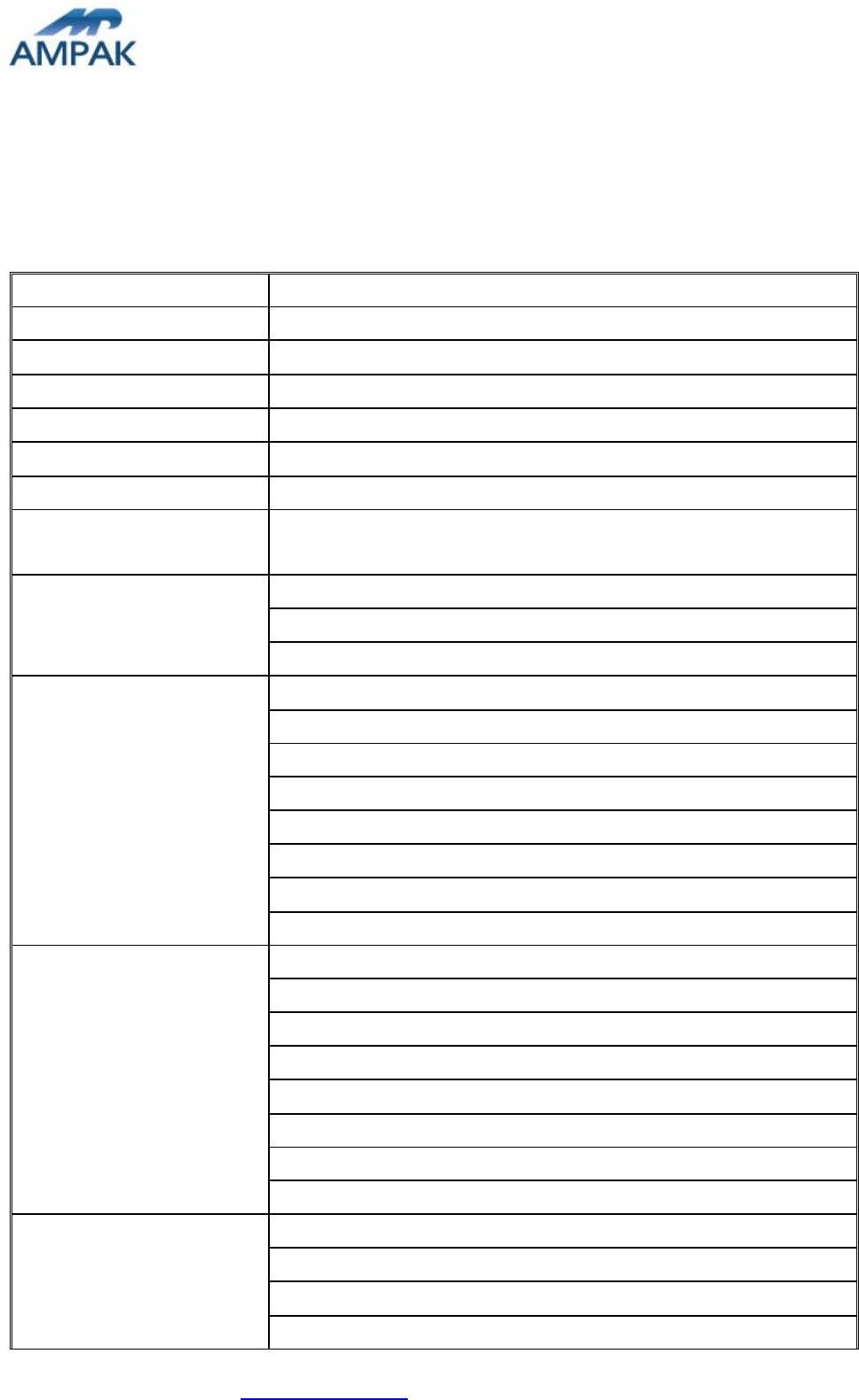
4. General Specification
4.1 Wi-Fi RF Specification
Conditions : VBAT=3.6V ; VDDIO=3.3V ; Temp:25°C
Feature Description
Product Name WL-211 Wi-Fi SIP Module
WLAN Standard IEEE 802.11b/g/n, WiFi compliant
Host Interface SDIO
Dimension L x W x H: 9.5 x 9.5 x 1.5 (typical) mm
Frequency Range 2.412 GHz ~ 2.4835 GHz (2.4 GHz ISM Band)
Number of Channels 11 for North America, 13 for Europe, and 14 for Japan
Modulation 802.11b : DQPSK, DBPSK, CCK
802.11g/n : OFDM /64-QAM,16-QAM, QPSK, BPSK
802.11b /11Mbps : 16 dBm ± 1.5 dB @ EVM -9dB
802.11g /54Mbps : 15 dBm ± 1.5 dB @ EVM -25dB
Output Power
802.11n /65Mbps : 14 dBm ± 1.5 dB @ EVM -28dB
- MCS=0 PER @ -85 ± 1dBm, typical
- MCS=1 PER @ -84 ± 1dBm, typical
- MCS=2 PER @ -82 ± 1dBm, typical
- MCS=3 PER @ -80 ± 1dBm, typical
- MCS=4 PER @ -77 ± 1dBm, typical
- MCS=5 PER @ -73 ± 1dBm, typical
- MCS=6 PER @ -71 ± 1dBm, typical
Receive Sensitivity
(11n,20MHz)
@10% PER
- MCS=7 PER @ -69 ± 1dBm, typical
- 6Mbps PER @ -87 ± 1dBm, typical
- 9Mbps PER @ -86 ± 1dBm, typical
- 12Mbps PER @ -85 ± 1dBm, typical
- 18Mbps PER @ -83 ± 1dBm, typical
- 24Mbps PER @ -81 ± 1dBm, typical
- 36Mbps PER @ -78 ± 1dBm, typical
- 48Mbps PER @ -74 ± 1dBm, typical
Receive Sensitivity (11g)
@10% PER
- 54Mbps PER @ -72 ± 1dBm, typical
- 1Mbps PER @ -90 ± 1dBm, typical
- 2Mbps PER @ -89 ± 1dBm, typical
- 5.5Mbps PER @ -87 ± 1dBm, typical
Receive Sensitivity (11b)
@8% PER
- 11Mbps PER @ -84 ± 1dBm, typical
Only for TPV.
AMPAK Technology Inc. www.ampak.com.tw Proprietary & Confidential Information
Doc. NO:
7
802.11b : 1, 2, 5.5, 11Mbps
Data Rate
802.11g : 6, 9, 12, 18, 24, 36, 48, 54Mbps
Data Rate
(20MHz ,Long GI,800ns)
802.11n: 6.5, 13, 19.5, 26, 39, 52, 58.5, 65Mbps
Data Rate
(20MHz ,short GI,400ns)
802.11n : 7.2, 14.4, 21.7, 28.9, 43.3, 57.8, 65,72.2Mbps
802.11b : -10 dBm
Maximum Input Level 802.11g/n : -20 dBm
Operating temperature -30°C to 85°C
Storage temperature -40°C to 85°C
Humidity Operating Humidity 10% to 95% Non-Condensing
Storage Humidity 5% to 95% Non-Condensing
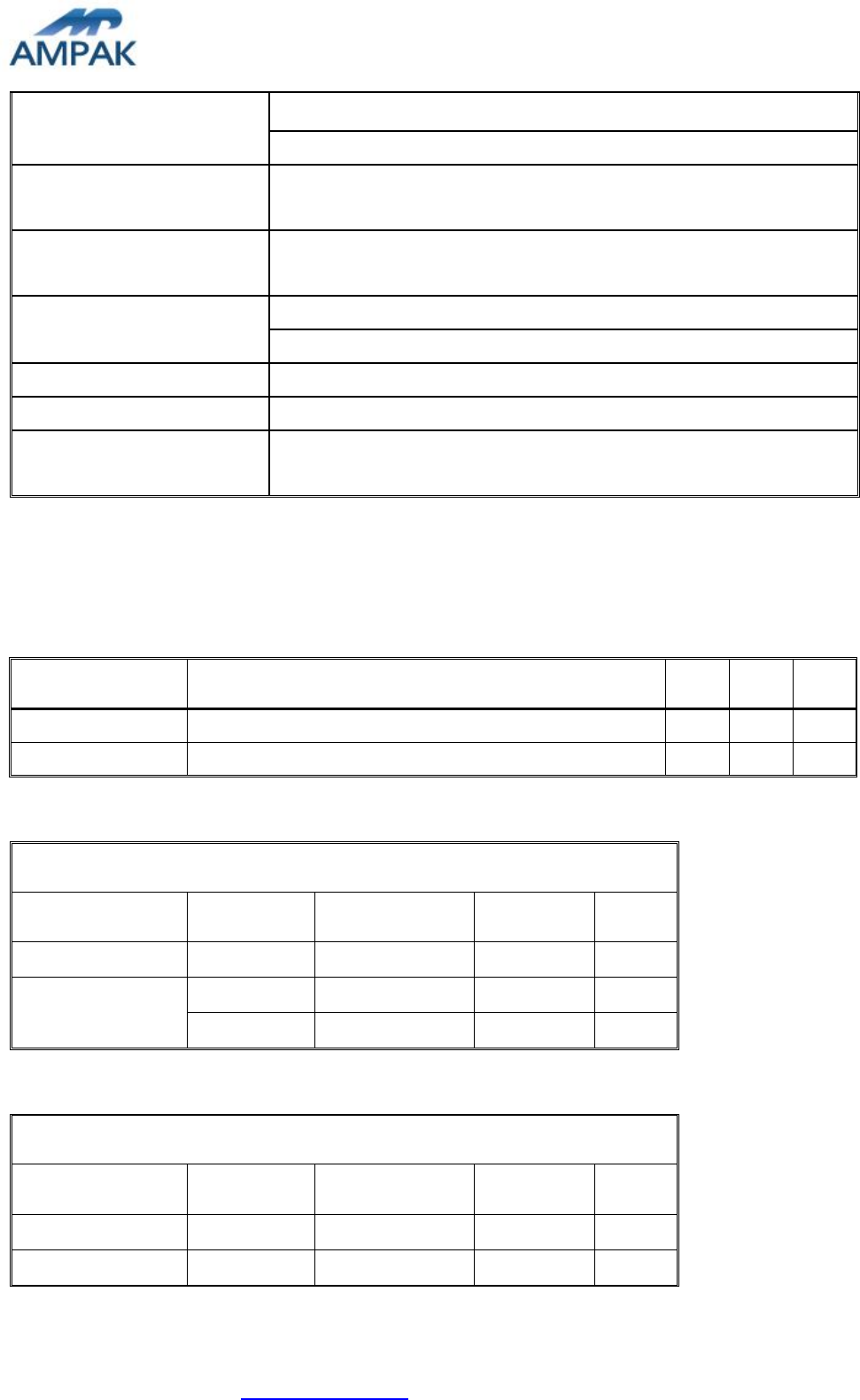
4.2 Voltages
4.2.1 Absolute Maximum Ratings
Symbol Description Min.
Max.
Unit
VBAT Input supply Voltage -0.5
6.5 V
VDDIO Digital/Bluetooth/SDIO/SPI I/O Voltage -0.5
4.1 V
4.2.2 Recommended Operating Ratings
Test conditions: At room temperature 25°C
Symbol Min. Typ. Max. Unit
VBAT 3.0 3.6 4.8 V
1.7 1.8 1.92 V
VDDIO 2.97 3.3 3.6 V
Note: The voltage of VDDIO is depended on system I/O voltage.
Test conditions: At operating temperature -10°C ~65°C
Symbol Min. Typ. Max. Unit
VBAT 3.0 3.6 4.8 V
VDDIO 1.7 - 3.35 V
Note: VDDIO operating voltage range from 1.7V to 3.35V at operating temperature is guaranteed.
Only for TPV.
AMPAK Technology Inc. www.ampak.com.tw Proprietary & Confidential Information
Doc. NO:
8
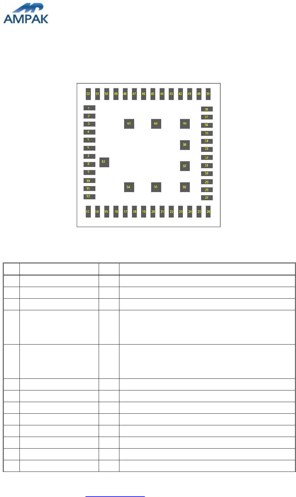
5. Pin Assignments
5.1 PCB Pin Outline
< TOP VIEW >
5.2 Pin Definition
NO
Name Type
Description
1 WLAN_ANT I/O
RF signal I/O port
2 GND - Ground
3 JTAG_TRST_L I JTAG interface, if JTAG not used unconnected (NC)
4 JTAG_TDO_UART_TX
O
JTAG interface, if JTAG not used unconnected (NC)
this pin. This pin is also muxed with UART_TX,
which can be enabled by software
5 JTAG_TDI_UART_RX
I
JTAG i
nterface, if JTAG not used unconnected (NC)
this pin. This pin is also muxed with UART_RX,
which can be enabled by software
6 JTAG_TCK I JTAG interface, if JTAG not used unconnected (NC)
7 JTAG_TMS I JTAG interface, if JTAG not used unconnected (NC)
8 GND - Ground
9 OSC_IN I XTAL oscillator input
10
OSC_OUT I/O
XTAL oscillator output
11
GND - Ground
12
RF_SW_CTRL0 - Floating (Don’t connected to ground)
13
RF_SW_CTRL3 - Floating (Don’t connected to ground)
Only for TPV.

AMPAK Technology Inc. www.ampak.com.tw Proprietary & Confidential Information
Doc. NO:
9
14
GND - Ground
15
GND - Ground
16
GND - Ground
17
GND - Ground
18
VIO I Digital I/O Voltage input
19
CLK_32K I Sleep clock (32.768KHz) input
20
SDIO_DATA_2 I/O
SDIO data line 2
21
SDIO_DATA_0 I/O
SDIO data line 0
22
SDIO_CLK I SDIO clock
23
SDIO_CMD I/O
SDIO command line
24
SDIO_DATA_1 I/O
SDIO data line 1
25
SDIO_DATA_3 I/O
SDIO data line 3
26
VIN_LDO I Internal DC-DC regulator input
27
GND - Ground
28
SR_VLX O Internal DC-DC regulator output
29
GND - Ground
30
VBAT I DC voltage input
31
WL_RST_N I Active low WLAN reset signal
32
GND - Ground
33
GND - Ground
34
GND - Ground
35
GND - Ground
36
XTAL_PU O Floating (Don’t connected to ground)
37
GND - Ground
38
GND - Ground
39
GND - Ground
40
GND - Ground
41
GND - Ground
42
GND - Ground
43
VDD_TCXO - Floating (Don’t connected to ground)
44
GND - Ground
45
TCXO_IN - Floating (Don’t connected to ground)
46
GPIO_5 - Floating (Don’t connected to ground)
47
GPIO_4 - Floating (Don’t connected to ground)
48
GPIO_3 - Floating (Don’t connected to ground)
49
GPIO_1 O WL_Host Wake,
50
GPIO_0 - Mode selection, Low for SDIO, High for SPI mode
51
WRF_GPIO_OUT - Floating (Don’t connected to ground)
Only for TPV.

AMPAK Technology Inc. www.ampak.com.tw Proprietary & Confidential Information
Doc. NO:
10
52
GND - Ground
53
GND - Ground
54
GND - Ground
55
GND - Ground
56
GND - Ground
57
GND - Ground
58
GND - Ground
59
GND - Ground
60
GND - Ground
61
GND - Ground
Only for TPV.
AMPAK Technology Inc. www.ampak.com.tw Proprietary & Confidential Information
Doc. NO:
11
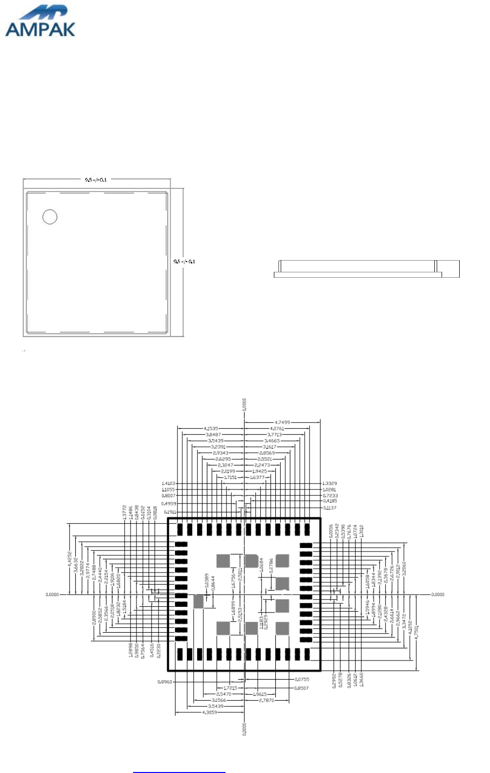
6. Dimensions
6.1 Physical Dimensions
(Unit: mm)
< TOP VIEW > < Side View >
< TOP VIEW >
1.7 (MAX)
Only for TPV.
AMPAK Technology Inc. www.ampak.com.tw Proprietary & Confidential Information
Doc. NO:
12
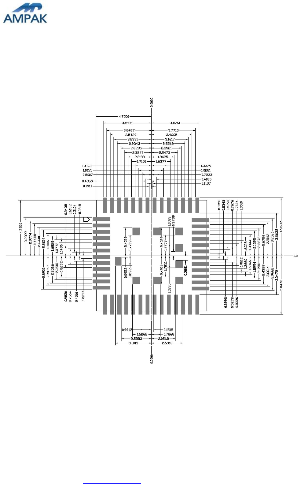
6.2 Recommended Footprint
(Unit: mm)
< TOP VIEW >
Only for TPV.

AMPAK Technology Inc. www.ampak.com.tw Proprietary & Confidential Information
Doc. NO:
13
7. External clock reference
External LPO signal characteristics
Parameter LPO Clock Units
Nominal input frequency 32.768 kHz
Frequency accuracy 30
ppm
Duty cycle 30 - 70 %
Input signal amplitude 1600 to 3300 mV, p-p
Signal type Square-wave or sine-wave
-
Input impedance >100k
<5
pF
Clock jitter (integrated over 300Hz – 15KHz) <1 Hz
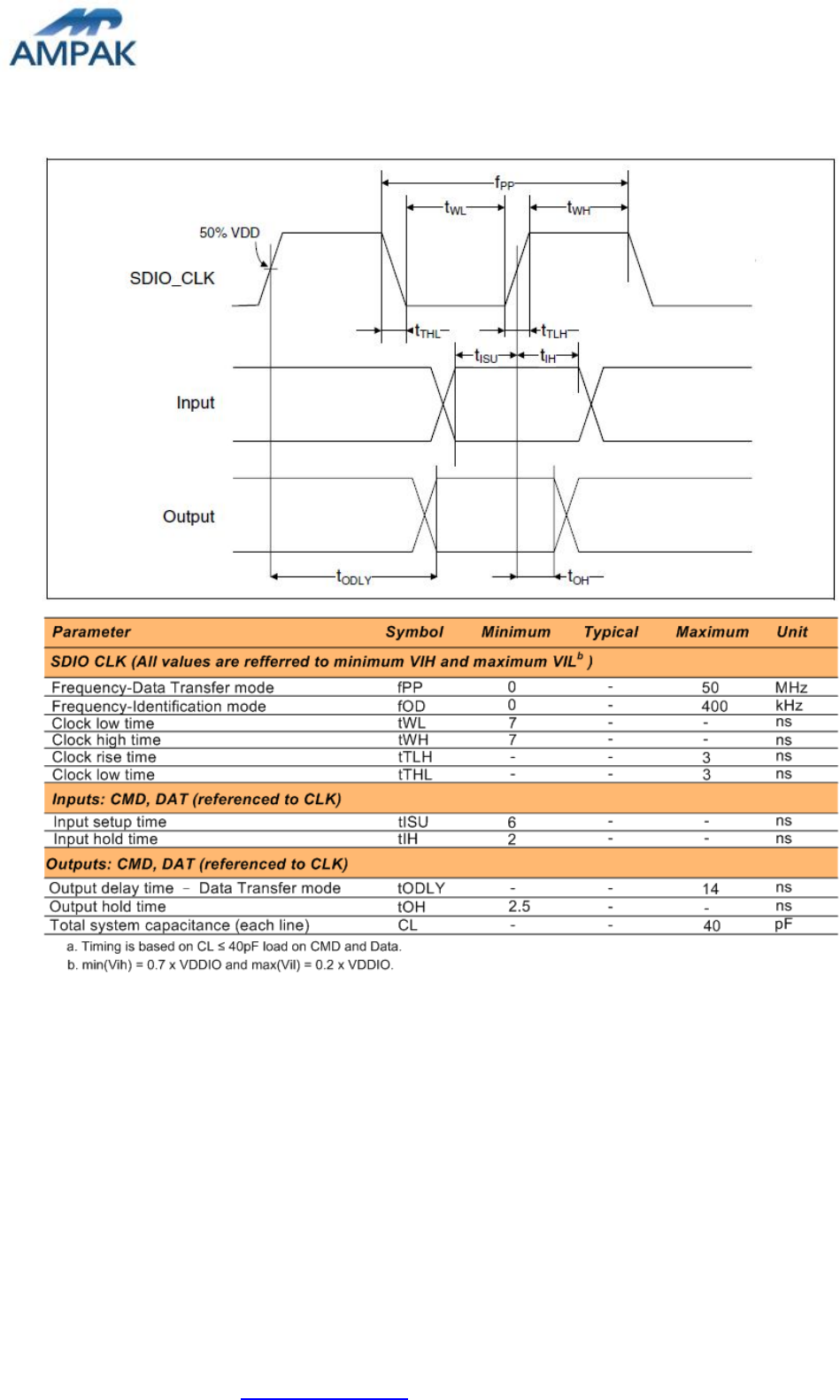
7.1 SDIO Pin Description
The WL-211 supports SDIO version 1.2 for both 1-bit (25 Mbps), 4-bit modes (100 Mbps),
and high speed 4-bit (50 MHz clocks – 200 Mbps). It has the ability to stop the SDIO clock
and map the interrupt signal into a GPIO pin. This ‘out-of-band’ interrupt signal notifies the
host when the WLAN device wants to turn on the SDIO interface. The ability to force the
control of the gated clocks from within the WLAN chip is also provided.
※ Function 0 Standard SDIO function (Max BlockSize / ByteCount = 32B)
※ Function 1 Backplane Function to access the internal System On Chip (SOC)
address space (Max BlockSize / ByteCount = 64B)
※ Function 2 WLAN Function for efficient WLAN packet transfer through DMA (Max
BlockSize / ByteCount = 512B)
SDIO Pin Description
SD 4-Bit Mode SD 1-Bit Mode SPI Mode
DATA0
Data Line 0 DATA
Data Line DO Data Output
DATA1
Data Line 1 or
Interrupt IRQ Interrupt IRQ Interrupt
DATA2
Data Line 2 or
Read Wait RW Read Wait NC Not Used
DATA3
Data Line 3 NC Not Used CS Card Select
CLK Clock CLK Clock SCLK
Clock
CMD Command Line CMD Command Line DI Data Input
Only for TPV.
AMPAK Technology Inc. www.ampak.com.tw Proprietary & Confidential Information
Doc. NO:
14
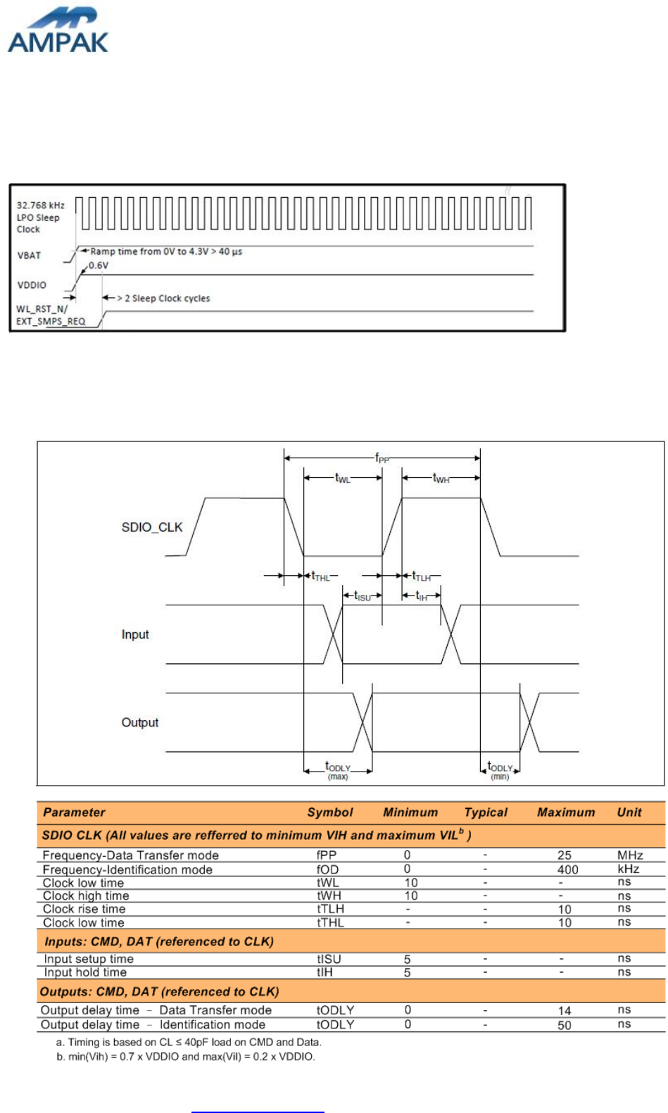
8. Host Interface Timing Diagram
8.1 Power-up Sequence Timing Diagram
※ WL_RST_N: Low asserting Reset for WLAN Core. This pin must be driven high or
low (not left floating).
8.2 SDIO Default Mode Timing Diagram
Only for TPV.
AMPAK Technology Inc. www.ampak.com.tw Proprietary & Confidential Information
Doc. NO:
15
8.3 SDIO High Speed Mode Timing Diagram
Only for TPV.
AMPAK Technology Inc. www.ampak.com.tw Proprietary & Confidential Information
Doc. NO:
16
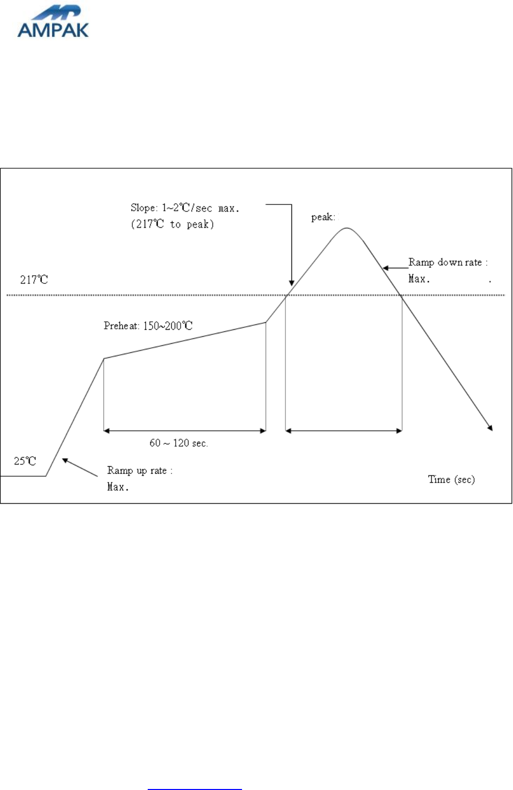
9. Recommended Reflow Profile
Referred to IPC/JEDEC standard.
Peak Temperature : <250°C
Number of Times : 2 times
10
2.5 /sec℃
2.5
°
C
/sec
40~70 sec
2
50
℃
Only for TPV.
AMPAK Technology Inc. www.ampak.com.tw Proprietary & Confidential Information
Doc. NO:
17
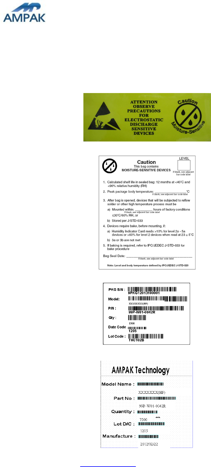
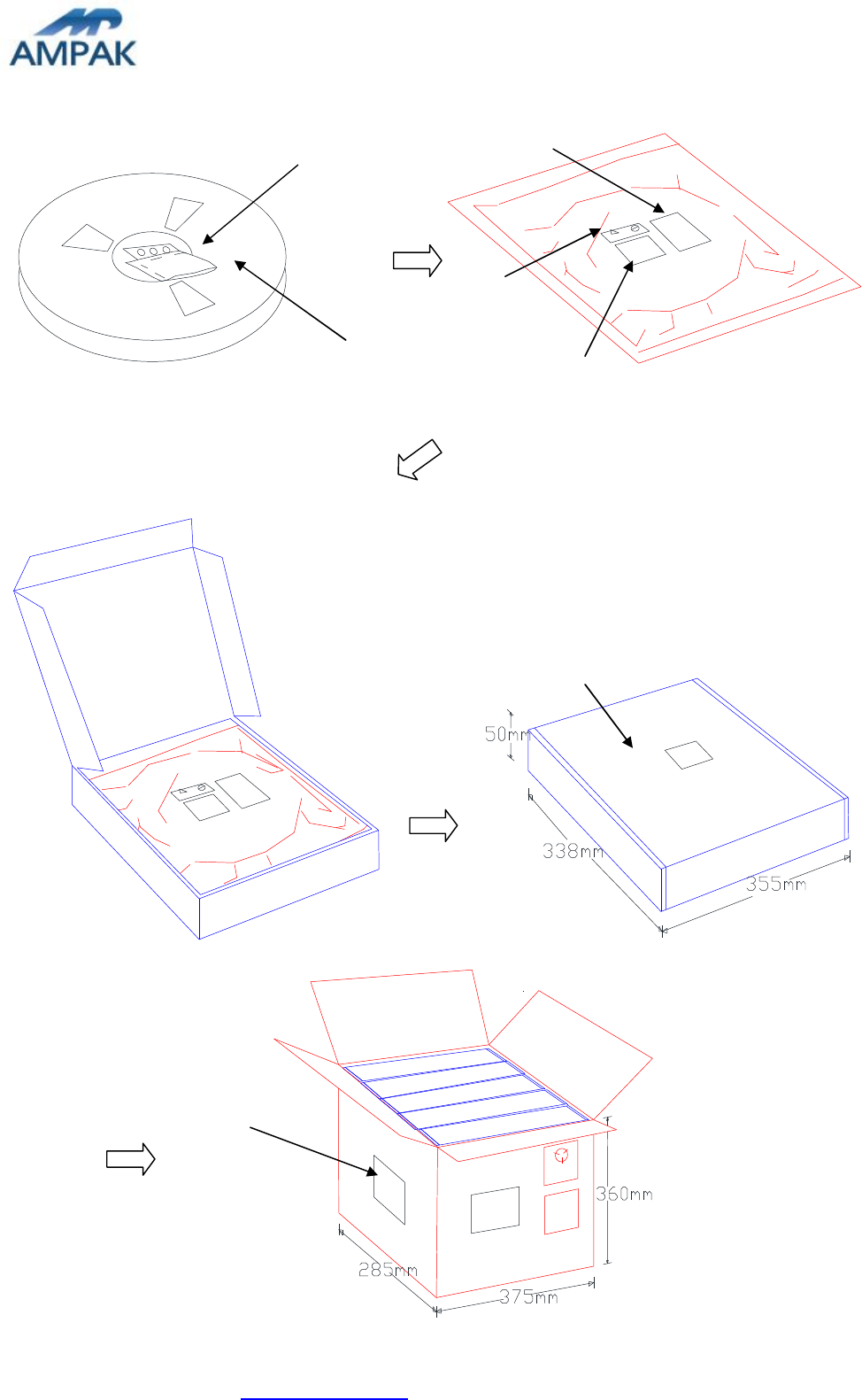
10. Packing Information
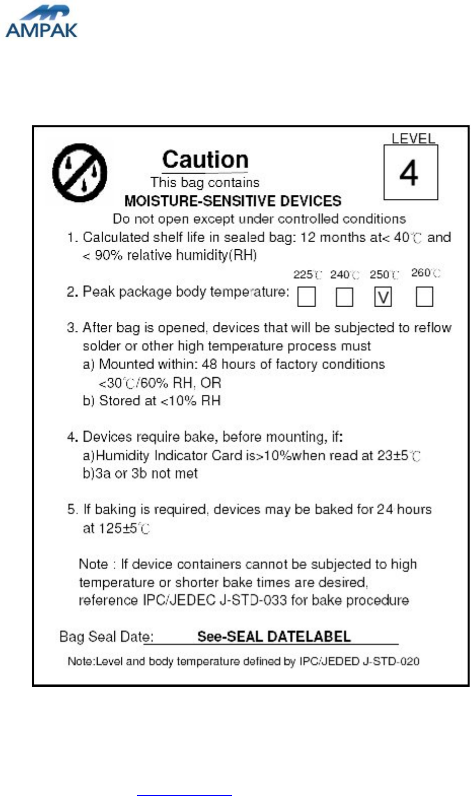
10.1 Label
Label A Anti-static and humidity notice
Label B MSL caution / Storage Condition
Label C Inner box label .
Label D Carton box label .
Only for TPV.
AMPAK Technology Inc. www.ampak.com.tw Proprietary & Confidential Information
Doc. NO:
18
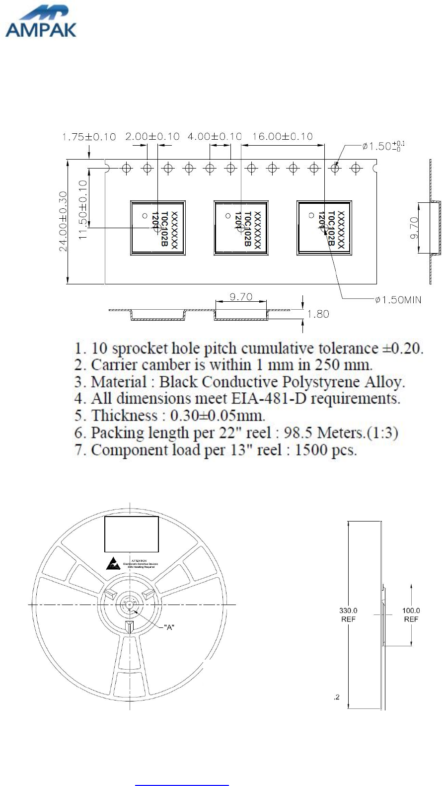
10.2 Dimension
Only for TPV.
AMPAK Technology Inc. www.ampak.com.tw Proprietary & Confidential Information
Doc. NO:
19
A
B
C
Humidity indicator
Desiccant
C
D
Only for TPV.
AMPAK Technology Inc. www.ampak.com.tw Proprietary & Confidential Information
Doc. NO:
20
10.3 MSL Level / Storage Condition
※NOTE : Accumulated baking time should not exceed 96hrs
Only for TPV.

F
This d
e
the fo
l
interfe
r
includi
n
This e
q
Class
B
are des
i
residen
t
freque
n
instruc
t
Howev
e
installa
t
televisi
o
and on
,
followi
n
- Reo
r
- Incr
e
- Con
n
to w
h
- Con
s
FCC C
party r
e
equip
m
This tr
a
other a
n
F
ederal C
o
e
vice comp
l
l
lowing t
w
r
ence, and
n
g interfere
q
uipment h
a
B
digital de
i
gned to pr
o
t
ial install
a
n
cy energy
t
ions, may
e
r, there is
t
ion. If t
h
o
n recepti
o
,
the user i
s
n
g measur
e
r
ient or relo
c
e
ase the sep
n
ect the eq
u
h
ich the rec
s
ult the dea
l
aution: An
y
e
sponsible
f
m
ent.
a
nsmitter
m
n
tenna or tr
a
o
mmunicat
i
l
ies with P
a
o conditio
n
(2) this
d
n
ce that m
a
a
s been te
s
vice, purs
u
o
vide reaso
n
tion. This
e
and, if n
o
cause h
a
no guarant
e
h
is equipm
e
o
n, which
c
s
encourag
e
e
s:
c
ate the rec
a
ration bet
w
u
ipment int
o
eiver is co
n
l
er or an ex
p
y
changes
o
f
or complia
n
m
ust not be
a
nsmitter.
ion Comm
a
rt 15 of t
h
ns: (1) T
h
d
evice mu
s
a
y cause un
d
s
ted and f
o
u
ant to Part
n
able prote
c
e
quipment
o
t installe
d
a
rmful int
e
e
e that inte
r
e
nt does c
a
c
an be dete
r
e
d to try to
eiving ante
n
w
een the e
q
o
an outlet
o
n
nected.
p
erienced r
a
or modific
a
n
ce could
v
co-located
i
ssion Inte
r
h
e FCC Rul
h
is device
s
t accept
a
d
esired ope
r
o
und to co
m
15 of the
F
c
tion again
s
generates,
u
d
and use
d
e
rference t
o
r
ference w
i
a
use harmf
u
r
mined by
correct the
n
na.
q
uip
m
ent a
n
o
n a circuit
d
a
dio/TV te
c
a
tions not
e
v
oid the use
or operati
n
r
ference S
t
es. Operati
o
may not
a
ny interfe
r
r
ation.
m
ply with
t
F
CC Rules
s
t harmful i
u
ses and c
a
d
in accor
d
o
radio c
o
i
ll not occu
r
u
l interfere
n
turning th
e
interferenc
d receiver.
d
ifferent fr
o
c
hnician for
e
xpressly a
p
r
's authorit
y
n
g in conju
n
t
atement
on is subje
cause har
m
r
ence rece
i
t
he limits
f
. These l
i
i
nterferenc
e
a
n radiate
r
d
ance wit
h
o
mmunicat
i
r
in a parti
c
n
ce to rad
i
e
equipmen
c
e by one o
f
o
m that
r
help.
p
p
r
oved b
y
y
to operat
e
n
ction wit
h
21
c
t to
m
ful
i
ved,
f
or a
i
mits
e
in a
r
adio
the
i
ons.
c
ular
i
o or
t
off
f
the
y
the
e
this
h
any

This devi
c
1) Th
e
ant
e
2) Th
e
or
a
As lon
g
require
d
end-pr
o
modul
e
IMPO
R
exampl
then th
e
not
b
e
u
will be
and ob
t
End Pr
o
FOR
M
This tr
a
may be
users.
T
followin
used o
n
c
e is intende
d
e
antenna
m
e
nna and us
e
transmitte
r
a
ntenna.
g
as 2 cond
i
d
. Howeve
r
o
duct for a
n
e
installe
d
R
TANT N
O
e certain la
p
e
FCC auth
o
u
sed on the
responsibl
e
t
aining a se
p
o
duct
Labe
M
OBILE D
a
nsmitter m
o
installed s
u
T
he final en
d
ng: “Contai
n
ly when al
l
d
only for
O
m
ust be inst
a
ers, and
r
module m
tions abov
e
r
, the OEM
n
y additiona
O
TE: In th
e
p
top config
o
rization is
final pro
d
u
e
for re-eva
l
p
arate FCC
l
in
g
EVICE U
S
o
dule is au
t
u
ch that 20
d
product
m
ins FCC ID
l
FCC com
p
O
EM integr
a
a
lled such t
h
m
ay not be c
o
e
are met, f
u
integrator i
a
l complian
c
e
event that
g
urations or
no longer
c
u
ct. In these
l
uating the
authorizati
S
AGE (>2
0
t
horized on
l
cm may be
m
ust be lab
e
:ARS-WL211
p
liance req
u
a
tors under
h
at 20 cm i
s
o
-located
w
u
rther trans
m
s
still respo
c
e require
m
these cond
i
co-locatio
n
c
onsidered
v
circumsta
n
end produc
on.
0
cm/low po
w
l
y for use i
n
maintaine
d
e
led in a vis
”. The
u
irements a
r
the followi
n
maintaine
d
w
ith any oth
e
m
itte
r
test
w
n
sible for t
e
m
ents requir
e
i
tions can n
n
with anot
h
v
alid and t
h
n
ces, the O
E
t
(includin
g
w
er)
n
device w
h
d
between t
h
i
ble area w
i
grantee's
r
e met.
n
g conditio
n
d
between t
h
e
r transmit
t
w
ill not be
e
sting their
e
d with this
n
ot be met (
f
h
er transmit
t
h
e FCC ID
c
E
M integrat
o
g
the trans
m
h
ere the ant
e
h
e antenna
a
i
th the
FCC ID can
22
n
s:
h
e
t
er
f
or
t
er),
c
an
o
r
m
itter)
e
nna
a
nd
be
Manuaal Informattion To the End User
The OE
EM integrat
regardinng how to i
end prooduct whic
The endd
as showw
oor has to b
nnstall or re
hh integrates
user manuual shall in
in this mannual.
ee aware not to provide
mmove this RRF module i
tthis modulee.
cclude all reqquired regul
iinformationn to the end
nn the user’ss manual of
atory informm
user
the
ation/warnning